EP3431247A1 - Method for manufacturing rear cover, rear cover and electronic device having the same - Google Patents
Method for manufacturing rear cover, rear cover and electronic device having the same Download PDFInfo
- Publication number
- EP3431247A1 EP3431247A1 EP18182913.6A EP18182913A EP3431247A1 EP 3431247 A1 EP3431247 A1 EP 3431247A1 EP 18182913 A EP18182913 A EP 18182913A EP 3431247 A1 EP3431247 A1 EP 3431247A1
- Authority
- EP
- European Patent Office
- Prior art keywords
- slot
- metal layer
- rear cover
- housing
- layer
- Prior art date
- Legal status (The legal status is an assumption and is not a legal conclusion. Google has not performed a legal analysis and makes no representation as to the accuracy of the status listed.)
- Granted
Links
Images








Classifications
-
- H—ELECTRICITY
- H01—ELECTRIC ELEMENTS
- H01Q—ANTENNAS, i.e. RADIO AERIALS
- H01Q1/00—Details of, or arrangements associated with, antennas
- H01Q1/12—Supports; Mounting means
- H01Q1/22—Supports; Mounting means by structural association with other equipment or articles
- H01Q1/24—Supports; Mounting means by structural association with other equipment or articles with receiving set
- H01Q1/241—Supports; Mounting means by structural association with other equipment or articles with receiving set used in mobile communications, e.g. GSM
- H01Q1/242—Supports; Mounting means by structural association with other equipment or articles with receiving set used in mobile communications, e.g. GSM specially adapted for hand-held use
- H01Q1/243—Supports; Mounting means by structural association with other equipment or articles with receiving set used in mobile communications, e.g. GSM specially adapted for hand-held use with built-in antennas
-
- B—PERFORMING OPERATIONS; TRANSPORTING
- B29—WORKING OF PLASTICS; WORKING OF SUBSTANCES IN A PLASTIC STATE IN GENERAL
- B29C—SHAPING OR JOINING OF PLASTICS; SHAPING OF MATERIAL IN A PLASTIC STATE, NOT OTHERWISE PROVIDED FOR; AFTER-TREATMENT OF THE SHAPED PRODUCTS, e.g. REPAIRING
- B29C39/00—Shaping by casting, i.e. introducing the moulding material into a mould or between confining surfaces without significant moulding pressure; Apparatus therefor
- B29C39/02—Shaping by casting, i.e. introducing the moulding material into a mould or between confining surfaces without significant moulding pressure; Apparatus therefor for making articles of definite length, i.e. discrete articles
- B29C39/10—Shaping by casting, i.e. introducing the moulding material into a mould or between confining surfaces without significant moulding pressure; Apparatus therefor for making articles of definite length, i.e. discrete articles incorporating preformed parts or layers, e.g. casting around inserts or for coating articles
-
- B—PERFORMING OPERATIONS; TRANSPORTING
- B29—WORKING OF PLASTICS; WORKING OF SUBSTANCES IN A PLASTIC STATE IN GENERAL
- B29C—SHAPING OR JOINING OF PLASTICS; SHAPING OF MATERIAL IN A PLASTIC STATE, NOT OTHERWISE PROVIDED FOR; AFTER-TREATMENT OF THE SHAPED PRODUCTS, e.g. REPAIRING
- B29C45/00—Injection moulding, i.e. forcing the required volume of moulding material through a nozzle into a closed mould; Apparatus therefor
- B29C45/14—Injection moulding, i.e. forcing the required volume of moulding material through a nozzle into a closed mould; Apparatus therefor incorporating preformed parts or layers, e.g. injection moulding around inserts or for coating articles
- B29C45/14311—Injection moulding, i.e. forcing the required volume of moulding material through a nozzle into a closed mould; Apparatus therefor incorporating preformed parts or layers, e.g. injection moulding around inserts or for coating articles using means for bonding the coating to the articles
-
- B—PERFORMING OPERATIONS; TRANSPORTING
- B29—WORKING OF PLASTICS; WORKING OF SUBSTANCES IN A PLASTIC STATE IN GENERAL
- B29C—SHAPING OR JOINING OF PLASTICS; SHAPING OF MATERIAL IN A PLASTIC STATE, NOT OTHERWISE PROVIDED FOR; AFTER-TREATMENT OF THE SHAPED PRODUCTS, e.g. REPAIRING
- B29C45/00—Injection moulding, i.e. forcing the required volume of moulding material through a nozzle into a closed mould; Apparatus therefor
- B29C45/14—Injection moulding, i.e. forcing the required volume of moulding material through a nozzle into a closed mould; Apparatus therefor incorporating preformed parts or layers, e.g. injection moulding around inserts or for coating articles
- B29C45/14336—Coating a portion of the article, e.g. the edge of the article
- B29C45/14344—Moulding in or through a hole in the article, e.g. outsert moulding
-
- B—PERFORMING OPERATIONS; TRANSPORTING
- B29—WORKING OF PLASTICS; WORKING OF SUBSTANCES IN A PLASTIC STATE IN GENERAL
- B29C—SHAPING OR JOINING OF PLASTICS; SHAPING OF MATERIAL IN A PLASTIC STATE, NOT OTHERWISE PROVIDED FOR; AFTER-TREATMENT OF THE SHAPED PRODUCTS, e.g. REPAIRING
- B29C67/00—Shaping techniques not covered by groups B29C39/00 - B29C65/00, B29C70/00 or B29C73/00
- B29C67/004—Closing perforations or small holes, e.g. using additional moulding material
-
- B—PERFORMING OPERATIONS; TRANSPORTING
- B29—WORKING OF PLASTICS; WORKING OF SUBSTANCES IN A PLASTIC STATE IN GENERAL
- B29C—SHAPING OR JOINING OF PLASTICS; SHAPING OF MATERIAL IN A PLASTIC STATE, NOT OTHERWISE PROVIDED FOR; AFTER-TREATMENT OF THE SHAPED PRODUCTS, e.g. REPAIRING
- B29C70/00—Shaping composites, i.e. plastics material comprising reinforcements, fillers or preformed parts, e.g. inserts
- B29C70/68—Shaping composites, i.e. plastics material comprising reinforcements, fillers or preformed parts, e.g. inserts by incorporating or moulding on preformed parts, e.g. inserts or layers, e.g. foam blocks
- B29C70/74—Moulding material on a relatively small portion of the preformed part, e.g. outsert moulding
- B29C70/745—Filling cavities in the preformed part
-
- H—ELECTRICITY
- H01—ELECTRIC ELEMENTS
- H01Q—ANTENNAS, i.e. RADIO AERIALS
- H01Q1/00—Details of, or arrangements associated with, antennas
- H01Q1/12—Supports; Mounting means
- H01Q1/22—Supports; Mounting means by structural association with other equipment or articles
-
- H—ELECTRICITY
- H01—ELECTRIC ELEMENTS
- H01Q—ANTENNAS, i.e. RADIO AERIALS
- H01Q13/00—Waveguide horns or mouths; Slot antennas; Leaky-waveguide antennas; Equivalent structures causing radiation along the transmission path of a guided wave
- H01Q13/10—Resonant slot antennas
- H01Q13/103—Resonant slot antennas with variable reactance for tuning the antenna
-
- H—ELECTRICITY
- H05—ELECTRIC TECHNIQUES NOT OTHERWISE PROVIDED FOR
- H05K—PRINTED CIRCUITS; CASINGS OR CONSTRUCTIONAL DETAILS OF ELECTRIC APPARATUS; MANUFACTURE OF ASSEMBLAGES OF ELECTRICAL COMPONENTS
- H05K5/00—Casings, cabinets or drawers for electric apparatus
- H05K5/02—Details
- H05K5/0247—Electrical details of casings, e.g. terminals, passages for cables or wiring
-
- B—PERFORMING OPERATIONS; TRANSPORTING
- B29—WORKING OF PLASTICS; WORKING OF SUBSTANCES IN A PLASTIC STATE IN GENERAL
- B29C—SHAPING OR JOINING OF PLASTICS; SHAPING OF MATERIAL IN A PLASTIC STATE, NOT OTHERWISE PROVIDED FOR; AFTER-TREATMENT OF THE SHAPED PRODUCTS, e.g. REPAIRING
- B29C45/00—Injection moulding, i.e. forcing the required volume of moulding material through a nozzle into a closed mould; Apparatus therefor
- B29C45/14—Injection moulding, i.e. forcing the required volume of moulding material through a nozzle into a closed mould; Apparatus therefor incorporating preformed parts or layers, e.g. injection moulding around inserts or for coating articles
- B29C45/14311—Injection moulding, i.e. forcing the required volume of moulding material through a nozzle into a closed mould; Apparatus therefor incorporating preformed parts or layers, e.g. injection moulding around inserts or for coating articles using means for bonding the coating to the articles
- B29C2045/14319—Injection moulding, i.e. forcing the required volume of moulding material through a nozzle into a closed mould; Apparatus therefor incorporating preformed parts or layers, e.g. injection moulding around inserts or for coating articles using means for bonding the coating to the articles bonding by a fusion bond
-
- B—PERFORMING OPERATIONS; TRANSPORTING
- B29—WORKING OF PLASTICS; WORKING OF SUBSTANCES IN A PLASTIC STATE IN GENERAL
- B29C—SHAPING OR JOINING OF PLASTICS; SHAPING OF MATERIAL IN A PLASTIC STATE, NOT OTHERWISE PROVIDED FOR; AFTER-TREATMENT OF THE SHAPED PRODUCTS, e.g. REPAIRING
- B29C45/00—Injection moulding, i.e. forcing the required volume of moulding material through a nozzle into a closed mould; Apparatus therefor
- B29C45/16—Making multilayered or multicoloured articles
- B29C2045/1693—Making multilayered or multicoloured articles shaping the first molding material before injecting the second molding material, e.g. by cutting, folding
-
- B—PERFORMING OPERATIONS; TRANSPORTING
- B29—WORKING OF PLASTICS; WORKING OF SUBSTANCES IN A PLASTIC STATE IN GENERAL
- B29K—INDEXING SCHEME ASSOCIATED WITH SUBCLASSES B29B, B29C OR B29D, RELATING TO MOULDING MATERIALS OR TO MATERIALS FOR MOULDS, REINFORCEMENTS, FILLERS OR PREFORMED PARTS, e.g. INSERTS
- B29K2705/00—Use of metals, their alloys or their compounds, for preformed parts, e.g. for inserts
-
- B—PERFORMING OPERATIONS; TRANSPORTING
- B29—WORKING OF PLASTICS; WORKING OF SUBSTANCES IN A PLASTIC STATE IN GENERAL
- B29K—INDEXING SCHEME ASSOCIATED WITH SUBCLASSES B29B, B29C OR B29D, RELATING TO MOULDING MATERIALS OR TO MATERIALS FOR MOULDS, REINFORCEMENTS, FILLERS OR PREFORMED PARTS, e.g. INSERTS
- B29K2995/00—Properties of moulding materials, reinforcements, fillers, preformed parts or moulds
- B29K2995/0003—Properties of moulding materials, reinforcements, fillers, preformed parts or moulds having particular electrical or magnetic properties, e.g. piezoelectric
-
- B—PERFORMING OPERATIONS; TRANSPORTING
- B29—WORKING OF PLASTICS; WORKING OF SUBSTANCES IN A PLASTIC STATE IN GENERAL
- B29L—INDEXING SCHEME ASSOCIATED WITH SUBCLASS B29C, RELATING TO PARTICULAR ARTICLES
- B29L2009/00—Layered products
- B29L2009/003—Layered products comprising a metal layer
-
- B—PERFORMING OPERATIONS; TRANSPORTING
- B29—WORKING OF PLASTICS; WORKING OF SUBSTANCES IN A PLASTIC STATE IN GENERAL
- B29L—INDEXING SCHEME ASSOCIATED WITH SUBCLASS B29C, RELATING TO PARTICULAR ARTICLES
- B29L2031/00—Other particular articles
- B29L2031/34—Electrical apparatus, e.g. sparking plugs or parts thereof
- B29L2031/3431—Telephones, Earphones
- B29L2031/3437—Cellular phones
-
- B—PERFORMING OPERATIONS; TRANSPORTING
- B29—WORKING OF PLASTICS; WORKING OF SUBSTANCES IN A PLASTIC STATE IN GENERAL
- B29L—INDEXING SCHEME ASSOCIATED WITH SUBCLASS B29C, RELATING TO PARTICULAR ARTICLES
- B29L2031/00—Other particular articles
- B29L2031/34—Electrical apparatus, e.g. sparking plugs or parts thereof
- B29L2031/3481—Housings or casings incorporating or embedding electric or electronic elements
Definitions
- the present disclosure relates to the field of consumer electronics in general. More particularly, and without limitation, the disclosed embodiments relate to a rear cover and an electronic device having the same, and a method for manufacturing a rear cover.
- An electronic device such as a mobile phone or a tablet can include a metal housing.
- the metal housing needs to define slots to allow signals to transmits therethrough. Thus, the signals are not be shielded.
- a method for manufacturing a rear cover is provided.
- a housing having a metal layer and a plastic layer can be provided.
- the metal layer can include a first surface and a second surface.
- the plastic layer can be formed on the first surface.
- a slot can be defined in the metal layer. The slot can pass through the first surface and the second surface of the metal layer. An unshielded portion can be formed in the slot.
- a shell is provided.
- the shell can have the metal layer.
- the first surface of the metal layer can be exposed.
- a nanocrystallization process can be applied to the first surface.
- a molten plastic material can be injected onto the nanocrystallized first surface.
- the molten plastic material can be cured to form the plastic layer.
- the plastic material since the plastic material is easily to be molten and cured, the plastic material can be disposed into the slot in a molten state, and then the molten plastic material can be cured into a solid state. Therefore, the process of manufacturing the rear cover can be simplified, and the production efficiency can be improved.
- the plastic material can be easily to obtained, and the signals can not be shielded by the plastic material.
- a milling process can be applied to the metal layer of the housing, thus the slot can be defined.
- a processing manner of the housing is simplified and a high machining accuracy can be obtained.
- the production cost can be reduced and the production efficiency can be increased.
- the slot can also be defined by other methods such as a laser processing.
- the slot can extend into the plastic layer.
- the slot can extend into the plastic layer.
- the metal layer can be divided into two parts by the slot.
- the plastic layer can not shield signals.
- the electronic device can be capable of transmitting signals through the slot to the outside of the electronic device, and receiving signals from the outside of the electronic device through the slot.
- the slot can be filled with a molten unshielded material.
- a high temperature curing process can be applied to the molten unshielded material. In this way, it is facilitated to fill the slot with the unshielded material to form the unshielded portion.
- the slot can be filled with the molten unshielded material uniformly, thereby avoiding gaps between the unshielded portion and the metal layer and intervals in the unshielded portion. Thus, a product quality of the rear cover with the antenna slot can be improved.
- a flattening process can be applied to the cured unshielded material.
- a flattened second surface can be formed.
- the rear cover can have a better appearance.
- an anode oxidation process can be applied to the second surface.
- the second surface can have a high performance in corrosion resistance and a wear resistance, and a hardness of the rear cover can be enhanced.
- a service life of the rear cover can be increased.
- the unshielded portion can be made of a material different from the plastic layer.
- At least one through hole can be defined in the housing.
- the at least one through hole can be configured to accommodate components of an electronic device having the rear cover. In this way, it is facilitated to accommodate and/or expose the components of the electronic device through the at least one through hole. Thus, an assembly efficiency of the electronic device can be increased.
- the slot can extend along a contour of the housing.
- the contour of the housing can be substantially a rounded rectangle. and the slot can substantially have a C-shape.
- the rear cover can have a better appearance, and a length of the slot can be lengthened.
- more paths for transmitting signals can be provided.
- a performance of transmitting signals of the electronic device can be improved.
- a rear cover in one embodiment of the present disclosure, can include a housing and an unshielded portion.
- the housing can include a metal layer and a plastic layer; the metal layer can include a first surface and a second surface.
- the plastic layer can be formed on the first surface.
- the metal layer can define a slot therein. The slot can pass the first surface and the second surface of the metal layer.
- the unshielded portion can be disposed in the slot.
- the first surface can be a nanocrystallized surface.
- the second surface can be an anode oxidized surface.
- the unshielded portion can be made of a material different from the plastic layer.
- the slot can extend into the plastic layer; the unshielded portion can be partially embedded in the plastic layer.
- the unshielded portion can be associated with a color uniformity of the second surface.
- the slot can extend along a contour of the housing.
- the contour of the housing can be substantially a rounded rectangle, and the slot can substantially have a C-shape.
- an electronic device in one embodiment of the present disclosure, can include the rear cover as mentioned as any of the embodiments above and a fedding element.
- the metal layer can be divided into an upper element and a main element, the slot can be formed between the upper element and the main element.
- the feeding element can be electrically coupled to the upper element of the metal layer.
- An antenna structure can be formed by the feeding element, the metal layer, and the slot. the upper element can be configured to be a main radiation element of the first antenna structure.
- an electronic device in one embodiment, can include base layer, a metal layer, an unshielded portion, and a feeding element.
- the metal layer can be attached on the base layer, and can include an upper element and a main element.
- a slot can be formed between the upper element and the main element.
- the unshielded portion can be at least partially disposed in the slot.
- the feeding element can be electrically coupled to the upper element of the metal layer.
- An antenna structure can be formed by the feeding element, the metal layer, and the slot.
- the upper element can be configured to be a main radiation element of the first antenna structure.
- an end of the feeding element extends across the slot and can be electrically coupled to the upper element, and another end of the feeding element can be coupled to a signal source
- the unshielded portion can be made of a basematerial different from the base layer.
- the slot can extend into the base layer.
- the unshielded portion is partially embedded in the base layer.
- the slot can extend into the plastic layer.
- the metal layer can be divided into two parts by the slot.
- the plastic layer can not shield signals.
- the electronic device can be capable of transmitting signals through the slot to the outside of the electronic device, and receiving signals from the outside of the electronic device through the slot.
- a “communication terminal” includes, but is not limited to, a device that is configured to receive/transmit communication signals via a wire line connection, such as via a public-switched telephone network (PSTN), digital subscriber line (DSL), digital cable, a direct cable connection, and/or another data connection/network, and/or via a wireless interface with, for example, a cellular network, a wireless local area network (WLAN)1 a digital television network such as a DVB-H network, a satellite network, an AM/FM broadcast transmitter, and/or another communication terminal.
- PSTN public-switched telephone network
- DSL digital subscriber line
- WLAN wireless local area network
- a digital television network such as a DVB-H network
- satellite network such as a satellite network
- AM/FM broadcast transmitter AM/FM broadcast transmitter
- a communication terminal that is configured to communicate over a wireless interface may be referred to as a "wireless communication terminal,” a “wireless terminal” and/or a “mobile terminal.”
- mobile terminals include, but are not limited to, a satellite or cellular radiotelephone; a Personal Communications System (PCS) terminal that may combine a cellular radiotelephone with data processing, facsimile and data communications capabilities; a PDA that can include a radiotelephone, pager, Internet/intranet access, Web browser, organizer, calendar and/or a global positioning system (GPS) receiver; and a conventional laptop and/or palmtop receiver or other appliance that includes a radiotelephone transceiver.
- PCS Personal Communications System
- GPS global positioning system
- the rear cover 10 can include a housing 12 and an unshielded portion 16 coupled to the housing 12.
- the housing 12 can define at least one antenna slot 14 therein, and the unshielded portion 16 can be received in the at least one slot 14.
- the housing 12 can include a metal layer 12 and a plastic layer 124.
- the metal layer 122 can include a first surface 1224 and a second surface 1224 departing from the first surface 1224.
- the second surface 1224 and the first surface 1224 can be respectively disposed at two departing side surfaces of the metal layer 122.
- Each one of the at least one slot 14 can pass through the second surface 1224 and the first surface 1224.
- the plastic layer 124 can be attached on and contacted with the first surface 1224.
- the method for manufacturing the rear cover 10 can begin at block S12.
- the housing 12 has a metal layer 122 and a plastic layer 124.
- the housing 12 can include a metal layer 122 and a plastic layer 124.
- the metal layer 122 can include a first surface 1224 and a second surface 1224 departing from the first surface 1224.
- the second surface 1224 and the first surface 1224 can be respectively disposed at two departing side surfaces of the metal layer 122.
- the plastic layer 124 can be formed on and contacted with the first surface 1224.
- the housing 12 can have the target shape, that is, a shape of the housing 12 can correspond to and match with a shape of the rear cover 10 of an electronic device 100.
- the electronic device 100 can be a mobile phone; and the rear cover 10 can be provided as a rear cover/battery cover of the mobile phone.
- the housing 12 can include a flat portion 126 and a sidewall 128 extending from a periphery of the flat portion 126.
- the sidewall 128 can include an exterior surface in an arc-shaped configuration.
- a method for manufacturing the housing 12 can begin at block S122.
- a shell is provided.
- the shell has the metal layer 122.
- a shell is provided.
- the shell can include the metal layer 122, and the first surface 1224 of the metal layer 122 can be exposed.
- a nanocrystallization process is applied to the first surface 1224.
- a molten plastic material is injected onto the nanocrystallized first surface 1224, and the molten plastic material is cured to form the plastic layer 124.
- the plastic layer 124 can be formed on and contacted with the metal layer 122, and the housing 12 with high quality can be obtained.
- a shape of the shell can match a target shape of the rear cover 10 of the electronic device 100. That is, the shell having the target shape should be processed in advance, and then be provided.
- the shell can be obtained by a stamping process, and then the plastic layer 124 can be formed on the shell.
- a manufacturing process of the housing 12 can be simplified.
- a slot 14 is defined in the metal layer 122.
- the slot 14 can pass the second surface 1224 and the first surface 1224 of the metal layer 122.
- the housing 12 can define one slot 14.
- the housing 12 can define two or more slots 14. That is, an amount of the slots 14 can be 1, 2, 3, 4 or more.
- a depth of the slot 14 can be greater than or equal to a thickness of the metal layer 122, and the depth of the slot 14 can be less than or equal to a sum of the thickness of the metal layer 122 and a thickness of the plastic layer 124.
- a method for defining the slot 14 can begin at block S142,
- a milling process is applied to the metal layer 122 to define the slot 14.
- the slot 14 can also be defined by other methods such as a laser processing.
- a method for defining the slot 14 can begin at block S144,
- a slot 14 is defined in the housing 12, and the slot 14 extends into the plastic layer 124.
- the slot 14 can extend from the second surface 1224 to the first surface 1224 and pass through the metal layer 122 to extend into the plastic layer 124.
- the slot 14 can extend into the plastic layer 124.
- the metal layer 122 can be divided into two parts by the slot 14.
- the plastic layer 124 can not shield signals.
- the electronic device 100 can be capable of transmitting signals through the slot 14 to the outside of the electronic device 100, and receiving signals from the outside of the electronic device 100 through the slot 14.
- the depth of the slot 14 can be greater than the thickness of the metal layer 122, while less than the sum of the thickness of the metal layer 122 and the thickness of the plastic layer 124. Therefore, the slot 14 can extend into the plastic layer 124 but does not pass through the plastic layer 124, and the unshielded portion 16 can be partially inserted into the plastic layer 124.
- the slot 14 can extend from a side of the house 12 to another side of the house 12.
- the sidewall 128 can include a first portion 1281 and a second portion 1283.
- the first portion 1281 and the second portion 1283 can be coupled to opposite sides of the flat portion 126, respectively.
- the first portion 1281 can be provided as a left border of the housing 12, while the second portion 1283 can be provided as a right border of the housing 12.
- the first portion 1281 can be provided as a top border of the housing 12, while the second portion 1283 can be provided as a bottom border of the housing 12. It can be understood that the above words of location of the housing 12 should be referred to a user's position when using the electronic device 100.
- the slot 14 can extend from the first portion 1281 to the second portion 1283. It can be understood that the slot 14 can extend from the first portion 1281, across the flat portion 126, to the second portion 1283 successively.
- the metal layer 122 can be made of aluminum alloy. Of course, in some alternative embodiments, the metal layer 122 can be made of other materials such as stainless steel or magnesium alloy.
- the metal layer 122 is divided into two parts by the slot 14. However, the slot 14 does not pass through the plastic layer 124. Thus, the two parts of the metal layer 122 can be coupled to each other by the plastic layer 124 and an unshielded portion 16 (formed at block S16). As a result, the housing 12 can remain as a whole component.
- the slot 14 may also completely pass through the metal layer 122 and the plastic layer 124 (as illustrated in FIG. 8 ).
- the depth of the slot 14 can be equal to the sum of the thicknesses of the metal layer 122 and the plastic layer 124.
- the housing 12 can be divided into two parts by the slot 14.
- the two parts of the metal layer 122 can be coupled to each other by the unshielded portion 16.
- a unshielded portion 16 is formed in the slot 14.
- an unshielded material can be disposed in the slot 14 to form the unshielded portion 16.
- the unshielded portion 16 can be completely or partially received in the slot 14. In this way, it is facilitated to fill the slot 14 with the unshielded material to form the unshielded portion 16.
- a method for forming the unshielded portion 16 can begin at block S162.
- the slot 14 is filled with a molten unshielded material.
- a high temperature curing process is applied to the molten unshielded material.
- the unshielded portion 16 can be formed and completely or partially received in the slot 14, and the rear cover 10 can be formed.
- the slot 14 can be filled with the molten unshielded material uniformly, thereby avoiding gaps between the unshielded portion 16 and the metal layer and intervals in the unshielded portion 16.
- a product quality of the rear cover 10 with the antenna slot 14 can be improved.
- the unshielded portion 16 may be made of plastic material. That is, the unshielded material can be a plastic material. The plastic material in a molten state may flow and may better fit with the slot 14 to fill the slot 14. After the slot 14 is filled with the molten unshielded material, the molten unshielded material is cured at a high temperature. Thus, the unshielded portion 16 can be formed in a solid state, and the unshielded portion 16 can be embedded in the metal layer 122.
- the unshielded portion 16 can be made of a material different from the plastic layer 124.
- the plastic material since the plastic material is easily to be molten and cured, the plastic material can be disposed into the slot 14 in a molten state, and then the molten plastic material can be cured into a solid state. Therefore, the process of manufacturing the rear cover 10 can be simplified, and the production efficiency can be improved. In addition, the plastic material can be easily to obtained, and the signals can not be shielded by the plastic material.
- the housing 12 in the method for manufacturing the rear cover 10, can be provided with a configuration of a target shaped in advanced, and then the slot 14 is defined in the housing 12.
- the rear cover 10 can be obtained after forming the unshielded portion 16 in the slot 14.
- a process of manufacturing the rear cover 10 is simplified, and a high utilization rate of raw materials can be achieved. Thus, the production efficiency can be increased and the production cost can be reduced.
- the rear cover 10 obtained by the method can be applied to an electronic device 100 (as illustrated in FIG. 3 ) such as a mobile phone, a tablet computer, or a smart wearable device.
- an electronic device 100 such as a mobile phone, a tablet computer, or a smart wearable device.
- One or more antennas disposed in the electronic device 100 can be capable of transmitting signals through the slot 14.
- the method for manufacturing the rear cover 10 can continue with block S18.
- a flattening process is applied to the cured unshielded material to form a flattened second surface 1224.
- a protruding portion 161 of the unshielded portion 16 protruding from the second surface 1224 can be removed, so that the second surface 1224 of the rear cover 10 is flattened.
- the molten unshielded material may overflow the slot 14.
- the protruding portion 161 protruding from the second surface 1224 may be formed.
- the protruding portion 161 should be removed to form a flattened second surface 1224. In this way, the rear cover 10 can have a better appearance.
- the second surface 1224 of the metal layer 122 can be considered as the second surface 1224 of the rear cover 10.
- the protruding portion 161 protruding from the second surface 1224 can be removed by a grinding or milling process. In other alternative embodiments, the protruding portion 161 can also be removed by a laser process.
- the second surface 1224 can be polished, so that the second surface 1224 of the rear cover 10 can have a better appearance.
- the slot 14 can be filled with the unshielded portion 16.
- the molten unshielded material does not overflow the slot 14, and the block S18 can be omitted.
- the depth of the slot 14 can be greater than a thickness of the unshielded portion 16.
- the method for manufacturing the rear cover 10 can further continue with block S19,
- an anode oxidation process is applied to the second surface 1224.
- the second surface 1224 can have a high performance in corrosion resistance and a wear resistance, and a hardness of the rear cover 10 can be enhanced. Thus, a service life of the rear cover 10 can be increased.
- the rear cover 10 can be applied to the electronic device 100 (as illustrated in FIG. 3 ).
- the housing 12 can define at least one through hole therein.
- the at least one through hole can be configured to accommodate and/or expose components of the electronic device 100.
- the electronic device 100 can include a camera 20 and a flasher 30.
- the camera 20 and the flasher 30 can be disposed in the housing 12.
- the housing 12 can define at least one through hole to expose the camera 20 and the flasher 30.
- the method for manufacturing the rear cover 10 can further continue with a method for defining at least one through hole in the housing.
- the housing 12 can define a first through hole 181 at a position corresponding to the camera 20, and a second through hole 183 at a position corresponding to the flasher 30.
- the first through hole 181 can be configured to expose the camera 20, so that the camera 20 can capture an image outside the electronic device 100.
- the second through hole 183 can be configured to expose the flashes 30.
- the light emitted from the flasher 30 can pass through the second through hole 183 to outside of the electronic device 100.
- a configuration of the slot 14 can be substantially C-shaped.
- the slot 14 in the metal layer 122 can extend along a contour of the housing 12.
- the contour of the housing 12 can be substantially a rounded rectangle.
- the slot 14 can be defined at an end of the housing 12 such that the slot 14 can substantially have a C-shape.
- the flat portion 126 can be substantially a rectangular plate, and the slot 14 can be defined at an end of the flat portion 126.
- the slot 14 can extend along a contour of the end of the flat portion 126.
- the slot 14 can include a first extending portion 141, a second extending portion 143, and a third extending portion 144.
- the second extending portion 143 and the third extending portion 144 can be coupled to two opposite ends of the first extending portion 141 respectively.
- the second extending portion 143 can be curved relative to the first extending portion 141.
- An end of the second extending portion 143 can start at the first portion 1281, and the second extending portion 143 can extend along the first portion 1281 to the flat portion 126.
- another end of the second extending portion 143 can be coupled to and communicate with the first extending portion 141.
- the third extending portion 144 can be curved relative to the first extending portion 141. An end of the third extending portion 144 can start at the second portion 1283, and the third extending portion 144 can extend along the second portion 1283 to the flat portion 126. Thus, another end of the third extending portion 144 can be coupled to and communicate with the first extending portion 141.
- the first extending portion 141, the second extending portion 143, and the third extending portion 144 corporately form the C-shaped structure of the slot 14.
- the slot 14 can extend on the first portion 1281, the flat portion 126 and the second portion 1283.
- the rear cover 10 can have a better appearance, and a length of the slot 14 can be lengthened.
- more paths for transmitting signals can be provided.
- a performance of transmitting signals of the electronic device 100 can be improved.
- the rear cover 10 can provide four slots 14 therein (as illustrated in FIG. 3 ).
- the rear cover 10 can further include a top end 101 and a bottom end 103 opposite to the top end 101.
- the rear cover 10 can define two slots 14 in the top end 101, and define two slots 14 in the bottom end 103.
- Each of the slots 14 can extend from the first portion 1281, across the flat portion 126 to the second portion 1283.
- the slot 14 can extend from a left border of the rear cover 10, and across the flat portion 126 to a right border of the rear cover 10.
- the slot 14 can pass the left and right sides of the rear cover 10.
- one or more slots 14 can be provided in the top end 101, while one or more slots 14 can be provided in the bottom end 103.
- the housing 12 having a target shaped is provided in advanced, and then the slot 14 is defined in the housing 12,
- the rear cover 10 can be obtained after forming the unshielded portion 16 in the slot 14.
- a process of manufacturing the rear cover 10 is simplified, and a high utilization rate of raw materials can be achieved, thus the production efficiency can be increased and the production cost can be reduced.
- the slot 14 can extend into the plastic layer 124.
- the unshielded portion 16 can be partially received in and coupled to the plastic layer 124.
- the unshielded portion 16 can be partially embedded in the plastic layer 124.
- the slot 14 can extend into the plastic layer 124.
- the metal layer 122 can be divided into two parts by the slot 14.
- the plastic layer 124 can not shield signals.
- the electronic device 100 can be capable of transmitting signals through the slot 14 to the outside of the electronic device 100, and receiving signals from the outside of the electronic device 100 through the slot 14.
- the unshielded portion 16 can be associated with a color uniformity of the second surface 1224. So that, the rear cover 10 can be more beautiful and the user experience can be improved.
- an electronic device 100 is provided.
- the electronic device 100 can include any of the rear covers 10 described above, and a cover plate (not illustrated).
- the cover plate can be coupled to the rear cover 10.
- the housing 12 having a target shaped is provided in advanced, and then the slot 14 is defined in the housing 12.
- the rear cover 10 can be obtained after forming the unshielded portion 16 in the slot 14.
- a process of manufacturing the rear cover 10 is simplified, and a high utilization rate of raw materials can be achieved, thus the production efficiency can be increased and the production cost can be reduced.
- an electronic device 100 is provided.
- the electronic device 100 may be a cellular phone, a tablet computer, or a notebook computer.
- the electronic device 100 can at least include a base layer 125, a metal layer 122, an unshielded portion 16, and a feeding element 190.
- the metal layer 122 can be attached to the base layer 125; the unshielded portion 16 and the feeding element 190 can be coupled to the metal layer 122.
- the feeding element 190 can be made of a metal such as silver, copper, or aluminum.
- the base layer 125 may be an FR4 substrate or a hard/soft composite board. In an alternative embodiment, the base layer 125 can be the plastic layer 124 described in the above embodiments.
- the electronic device 100 may further include other essential components, including but not limited to, a processing module, a touch module, a display module, a transparent panel, and a battery (not shown). Among them, the touch module may be integrated with the display module to form a touch-display module.
- the metal layer 122 can be stacked on the base layer 125.
- the metal layer 122 can include an upper element 1201 and a main element 1202 spaced from the upper element 1201.
- a slot 14 can be formed between the upper element 1201 and the main element 1202.
- the feeding element 190 can be configured to electrically connect the main element 1202 to the upper element 1201.
- the unshielded portion 16 can be at least partially disposed in the slot 14.
- the slot 14 may completely separate the upper element 1201 from the main element 1202.
- the electronic device 100 can further include a conductive element 1205, and the conductive element 1205 can extend across the slot 14 and electrically connect the upper element 1201 to the main element1202.
- the conductive element 1205 can be an FPCB (Flexible Printed Circuit Board).
- an antenna structure can be formed by the feeding element 190, the upper element 1201, and the slot 14.
- the upper element 1201 can be a main radiation element of the antenna structure.
- the feeding element 190 may be coupled to the upper element 1201 to excite the antenna structure.
- the electronic device 100 can further include a signal source 199 coupled to the main element 1202.
- An end of the feeding element 190 can be coupled to the signal source 199, and another end of the feeding element 190 can extend across the slot 14 and couple to the upper element 1201.
- the signal source 199 can be further coupled to an RF (Radio Frequency) signal processing module (not illustrated).
- the feeding element 190 and the metal layer 122 may be disposed on different planes.
- the feeding element 190 can be coupled through a metal spring (not illustrated) to the metal layer 120 to excite the antenna structure.
- the feeding element 190 may include a variable capacitor (not illustrated).
- the feeding element 190 can be a portion of the antenna structure of the electronic device 100. Even if the feeding element 190 extends across the slot 14, the feeding element 190 does not affect the radiation performance of the antenna structure. Electromagnetic waves may be transmitted or received through the slot 14 by the antenna structure. Accordingly, the antenna structure can maintain good radiation efficiency.
- the metal layer 122 can further include a lower element 1203.
- the lower element 1203 can be disposed at a side of the mian element 1202 far away from the upper element 1201, and can be spaced from the main element 1202.
- Another slot 14 can be formed between the main element 1202 and the lower element 1203.
- the electronic device 100 can further include a baseband chipset 910, an RF (Radio Frequency) module 920, and a matching circuit 930.
- the baseband chipset 910, the RF module 920, and the matching circuit 930 can be disposed on the main element 1202 of the metal layer 122.
- the baseband chipset 910 may be coupled through the RF module 920 and the matching circuit 930 to the feeding element 190 to excite the antenna structure of the electronic device 100.
- the baseband chipset 910 can be considered to be a signal source of the electronic device 100.
- the electronic device 100 can further include one or more electronic components 950, which may be disposed on the upper element 1201 or the lower element 1203.
- the electronic components 950 can include at least one of a speaker, a receiver, a microphone, a camera, a USB (Universal Serial Bus) socket, a memory card socket, a vibrator, and/or an audio jack.
- the electronic components 950 can be coupled through one or more metal traces 960 to the baseband chipset 910.
- the electronic components 950 can be disposed on a non-slot region of the antenna structure of the electronic device 100, and the electronic components 950 can be considered to be a portion of the antenna structure. Accordingly, the electronic components 950 do not affect the radiation performance of the antenna structure.
- the antenna structure can be integrated with the electronic components 950, and the inner space of the electronic device 100 can be effectively saved.
Landscapes
- Engineering & Computer Science (AREA)
- Mechanical Engineering (AREA)
- Manufacturing & Machinery (AREA)
- Microelectronics & Electronic Packaging (AREA)
- Chemical & Material Sciences (AREA)
- Composite Materials (AREA)
- Computer Networks & Wireless Communication (AREA)
- Telephone Set Structure (AREA)
- Casings For Electric Apparatus (AREA)
- Support Of Aerials (AREA)
- Details Of Aerials (AREA)
Abstract
Description
- This application claims priority to a Chinese application No.
201710602869.7 filed on July 21, 2017 - The present disclosure relates to the field of consumer electronics in general. More particularly, and without limitation, the disclosed embodiments relate to a rear cover and an electronic device having the same, and a method for manufacturing a rear cover.
- An electronic device such as a mobile phone or a tablet can include a metal housing. The metal housing needs to define slots to allow signals to transmits therethrough. Thus, the signals are not be shielded.
- In accordance with an aspect, in one embodiment of the present disclosure, a method for manufacturing a rear cover is provided. In the method, a housing having a metal layer and a plastic layer can be provided. The metal layer can include a first surface and a second surface. The plastic layer can be formed on the first surface. A slot can be defined in the metal layer. The slot can pass through the first surface and the second surface of the metal layer. An unshielded portion can be formed in the slot.
- In one embodiment, a shell is provided. The shell can have the metal layer. The first surface of the metal layer can be exposed. A nanocrystallization process can be applied to the first surface. A molten plastic material can be injected onto the nanocrystallized first surface. The molten plastic material can be cured to form the plastic layer. In this way, since the plastic material is easily to be molten and cured, the plastic material can be disposed into the slot in a molten state, and then the molten plastic material can be cured into a solid state. Therefore, the process of manufacturing the rear cover can be simplified, and the production efficiency can be improved. In addition, the plastic material can be easily to obtained, and the signals can not be shielded by the plastic material.
- In one embodiment, a milling process can be applied to the metal layer of the housing, thus the slot can be defined. In this way, a processing manner of the housing is simplified and a high machining accuracy can be obtained. Thus, the production cost can be reduced and the production efficiency can be increased. Of course, the slot can also be defined by other methods such as a laser processing.
- In one embodiment, the slot can extend into the plastic layer. In this way, the slot can extend into the plastic layer. Thus, the metal layer can be divided into two parts by the slot. In addition, the plastic layer can not shield signals. Thus, the electronic device can be capable of transmitting signals through the slot to the outside of the electronic device, and receiving signals from the outside of the electronic device through the slot.
- In one embodiment, the slot can be filled with a molten unshielded material. A high temperature curing process can be applied to the molten unshielded material. In this way, it is facilitated to fill the slot with the unshielded material to form the unshielded portion. The slot can be filled with the molten unshielded material uniformly, thereby avoiding gaps between the unshielded portion and the metal layer and intervals in the unshielded portion. Thus, a product quality of the rear cover with the antenna slot can be improved.
- In one embodiment, a flattening process can be applied to the cured unshielded material. Thus a flattened second surface can be formed. In this way, the rear cover can have a better appearance.
- In one embodiment, an anode oxidation process can be applied to the second surface. In this way, after the oxidation process, the second surface can have a high performance in corrosion resistance and a wear resistance, and a hardness of the rear cover can be enhanced. Thus, a service life of the rear cover can be increased.
- In one embodiment, the unshielded portion can be made of a material different from the plastic layer.
- In one embodiment, at least one through hole can be defined in the housing. The at least one through hole can be configured to accommodate components of an electronic device having the rear cover. In this way, it is facilitated to accommodate and/or expose the components of the electronic device through the at least one through hole. Thus, an assembly efficiency of the electronic device can be increased.
- In one embodiment, the slot can extend along a contour of the housing. The contour of the housing can be substantially a rounded rectangle. and the slot can substantially have a C-shape. In this way, the rear cover can have a better appearance, and a length of the slot can be lengthened. Thus, more paths for transmitting signals can be provided. Thus, a performance of transmitting signals of the electronic device can be improved.
- In accordance with another aspect, in one embodiment of the present disclosure, a rear cover is provided. The rear cover can include a housing and an unshielded portion. The housing can include a metal layer and a plastic layer; the metal layer can include a first surface and a second surface. The plastic layer can be formed on the first surface. The metal layer can define a slot therein. The slot can pass the first surface and the second surface of the metal layer. The unshielded portion can be disposed in the slot.
- In one embodiment, the first surface can be a nanocrystallized surface.
- In one embodiment, the second surface can be an anode oxidized surface.
- In one embodiment, the unshielded portion can be made of a material different from the plastic layer.
- In one embodiment, the slot can extend into the plastic layer; the unshielded portion can be partially embedded in the plastic layer.
- In one embodiment, the unshielded portion can be associated with a color uniformity of the second surface.
- In one embodiment, the slot can extend along a contour of the housing. The contour of the housing can be substantially a rounded rectangle, and the slot can substantially have a C-shape.
- In accordance with a still another aspect, in one embodiment of the present disclosure, an electronic device is provided. The electronic device can include the rear cover as mentioned as any of the embodiments above and a fedding element. The metal layer can be divided into an upper element and a main element, the slot can be formed between the upper element and the main element. The feeding element can be electrically coupled to the upper element of the metal layer. An antenna structure can be formed by the feeding element, the metal layer, and the slot. the upper element can be configured to be a main radiation element of the first antenna structure.
- In accordance with a still another aspect, in one embodiment of the present disclosure, an electronic device is provided. The electronic device can include base layer, a metal layer, an unshielded portion, and a feeding element. The metal layer can be attached on the base layer, and can include an upper element and a main element. A slot can be formed between the upper element and the main element. The unshielded portion can be at least partially disposed in the slot. The feeding element can be electrically coupled to the upper element of the metal layer. An antenna structure can be formed by the feeding element, the metal layer, and the slot. The upper element can be configured to be a main radiation element of the first antenna structure.
- In one embodiment, an end of the feeding element extends across the slot and can be electrically coupled to the upper element, and another end of the feeding element can be coupled to a signal source
- In one embodiment, the unshielded portion can be made of a basematerial different from the base layer.
- In one embodiment, the slot can extend into the base layer. The unshielded portion is partially embedded in the base layer.
- In this way, the slot can extend into the plastic layer. Thus, the metal layer can be divided into two parts by the slot. In addition, the plastic layer can not shield signals. Thus, the electronic device can be capable of transmitting signals through the slot to the outside of the electronic device, and receiving signals from the outside of the electronic device through the slot.
- The accompanying drawings, which are incorporated in and constitute a part of this specification, illustrate exemplary embodiments of the present disclosure, and together with the description, serve to explain the principles of the disclosure.
-
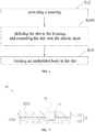
FIG. 1 illustrates a schematic flowchart of a method for manufacturing a rear cover, in accordance with one embodiment of the present disclosure. -
FIG. 2 illustrates a schematic view of a process of the method. -
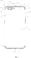
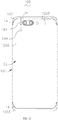
FIG. 3 illustrates a schematic view of an electronic device including a rear cover, in accordance with one embodiment of the present disclosure. -
FIG. 4 illustrates a schematic flowchart of a method for manufacturing a rear cover, in accordance with another embodiment of the present disclosure. -
FIG. 5 illustrates a schematic flowchart of a method for manufacturing a rear cover, in accordance with still another embodiment of the present disclosure. -
FIG. 6 illustrates a schematic flowchart of a method for manufacturing a rear cover, in accordance with further another embodiment of the present disclosure. -
FIG. 7 illustrates a partial cross-sectional schematic view of a rear cover, in accordance with one embodiment of the present disclosure. -
FIG. 8 illustrates a partial cross-sectional view of a rear cover, in accordance with another embodiment of the present disclosure. -
FIG. 9 illustrates a schematic flowchart of a method for manufacturing a rear cover, in accordance with still another embodiment of the present disclosure. -
FIG. 10 illustrates a schematic flowchart of a method of manufacturing a rear cover, in accordance with further another embodiment of the present disclosure. -
FIG. 11 illustrates a schematic flowchart of a method of manufacturing a rear cover, in accordance with further another embodiment of the present disclosure. -
FIG. 12 illustrates a schematic view of an electronic device including a rear cover, in accordance with further another embodiment of the present disclosure. -
FIG. 13 illustrates a schematic view of an electronic device including a rear cover, in accordance with further another embodiment of the present disclosure. -
FIG. 14 illustrates an enlarged view of area A ofFIG. 13 . - This description and the accompanying drawings that illustrate exemplary embodiments should not be taken as limiting. Various mechanical, structural, electrical, and operational changes may be made without departing from the scope of this description and the claims, including equivalents. In some instances, well known structures and techniques have not been shown or described in detail so as not to obscure the disclosure. Similar reference numbers in two or more figures represent the same or similar elements. Furthermore, elements and their associated features that are disclosed in detail with reference to one embodiment may, whenever practical, be included in other embodiments in which they are not specifically shown or described. For example, if an element is described in detail with reference to one embodiment and is not described with reference to a second embodiment, the element may nevertheless be claimed as included in the second embodiment.
- As used herein, a "communication terminal" (or simply a "terminal") includes, but is not limited to, a device that is configured to receive/transmit communication signals via a wire line connection, such as via a public-switched telephone network (PSTN), digital subscriber line (DSL), digital cable, a direct cable connection, and/or another data connection/network, and/or via a wireless interface with, for example, a cellular network, a wireless local area network (WLAN)1 a digital television network such as a DVB-H network, a satellite network, an AM/FM broadcast transmitter, and/or another communication terminal. A communication terminal that is configured to communicate over a wireless interface may be referred to as a "wireless communication terminal," a "wireless terminal" and/or a "mobile terminal." Examples of mobile terminals include, but are not limited to, a satellite or cellular radiotelephone; a Personal Communications System (PCS) terminal that may combine a cellular radiotelephone with data processing, facsimile and data communications capabilities; a PDA that can include a radiotelephone, pager, Internet/intranet access, Web browser, organizer, calendar and/or a global positioning system (GPS) receiver; and a conventional laptop and/or palmtop receiver or other appliance that includes a radiotelephone transceiver.
- As illustrated in
FIG. 1 andFIG. 2 , a method for manufacturing arear cover 10 is provided, in accordance with one embodiment of the present disclosure. Therear cover 10 can include ahousing 12 and anunshielded portion 16 coupled to thehousing 12. Thehousing 12 can define at least oneantenna slot 14 therein, and theunshielded portion 16 can be received in the at least oneslot 14. In one embodiment, thehousing 12 can include ametal layer 12 and aplastic layer 124. Themetal layer 122 can include afirst surface 1224 and asecond surface 1224 departing from thefirst surface 1224. Thesecond surface 1224 and thefirst surface 1224 can be respectively disposed at two departing side surfaces of themetal layer 122. Each one of the at least oneslot 14 can pass through thesecond surface 1224 and thefirst surface 1224. Theplastic layer 124 can be attached on and contacted with thefirst surface 1224. - In one embodiment, the method for manufacturing the
rear cover 10 can begin at block S12. - At block S12, a
housing 12 is provided. Thehousing 12 has ametal layer 122 and aplastic layer 124. - In one embodiment, the
housing 12 can include ametal layer 122 and aplastic layer 124. Themetal layer 122 can include afirst surface 1224 and asecond surface 1224 departing from thefirst surface 1224. Thesecond surface 1224 and thefirst surface 1224 can be respectively disposed at two departing side surfaces of themetal layer 122. Theplastic layer 124 can be formed on and contacted with thefirst surface 1224. - Specifically, the
housing 12 can have the target shape, that is, a shape of thehousing 12 can correspond to and match with a shape of therear cover 10 of anelectronic device 100. As illustrated inFIG. 3 , in accordance with one embodiment of the present disclosure, theelectronic device 100 can be a mobile phone; and therear cover 10 can be provided as a rear cover/battery cover of the mobile phone. Thehousing 12 can include aflat portion 126 and asidewall 128 extending from a periphery of theflat portion 126. Thesidewall 128 can include an exterior surface in an arc-shaped configuration. - As illustrated in
FIG. 4 , in some embodiments, a method for manufacturing thehousing 12 can begin at block S122. - At block S122, a shell is provided. The shell has the
metal layer 122. - In one embodiment, a shell is provided. The shell can include the
metal layer 122, and thefirst surface 1224 of themetal layer 122 can be exposed. - At block S124, a nanocrystallization process is applied to the
first surface 1224. - At block S126, a molten plastic material is injected onto the nanocrystallized
first surface 1224, and the molten plastic material is cured to form theplastic layer 124. - In this way, the
plastic layer 124 can be formed on and contacted with themetal layer 122, and thehousing 12 with high quality can be obtained. - Specifically, at block S122, a shape of the shell can match a target shape of the
rear cover 10 of theelectronic device 100. That is, the shell having the target shape should be processed in advance, and then be provided. For example, the shell can be obtained by a stamping process, and then theplastic layer 124 can be formed on the shell. Thus, a manufacturing process of thehousing 12 can be simplified. - At block S14, a
slot 14 is defined in themetal layer 122. - In one embodiment, the
slot 14 can pass thesecond surface 1224 and thefirst surface 1224 of themetal layer 122. In one embodiment, thehousing 12 can define oneslot 14. In some alternative embodiment, thehousing 12 can define two ormore slots 14. That is, an amount of theslots 14 can be 1, 2, 3, 4 or more. - In one embodiment, a depth of the
slot 14 can be greater than or equal to a thickness of themetal layer 122, and the depth of theslot 14 can be less than or equal to a sum of the thickness of themetal layer 122 and a thickness of theplastic layer 124. - As illustrated in
FIG. 5 , in some embodiments, a method for defining theslot 14 can begin at block S142, - At block S142, a milling process is applied to the
metal layer 122 to define theslot 14. - In this way, a processing manner of the
housing 12 is simplified and a high machining accuracy can be obtained. Thus, the production cost can be reduced and the production efficiency can be increased. Of course, theslot 14 can also be defined by other methods such as a laser processing. - As illustrated in
FIG. 6 and FIG. 7 , in some alternative embodiments, a method for defining theslot 14 can begin at block S144, - At block S144, a
slot 14 is defined in thehousing 12, and theslot 14 extends into theplastic layer 124. - In an alternative embodiment, the
slot 14 can extend from thesecond surface 1224 to thefirst surface 1224 and pass through themetal layer 122 to extend into theplastic layer 124. - In this way, the
slot 14 can extend into theplastic layer 124. Thus, themetal layer 122 can be divided into two parts by theslot 14. In addition, theplastic layer 124 can not shield signals. Thus, theelectronic device 100 can be capable of transmitting signals through theslot 14 to the outside of theelectronic device 100, and receiving signals from the outside of theelectronic device 100 through theslot 14. - In one embodiment, the depth of the
slot 14 can be greater than the thickness of themetal layer 122, while less than the sum of the thickness of themetal layer 122 and the thickness of theplastic layer 124. Therefore, theslot 14 can extend into theplastic layer 124 but does not pass through theplastic layer 124, and theunshielded portion 16 can be partially inserted into theplastic layer 124. - In an alternative embodiment, the
slot 14 can extend from a side of thehouse 12 to another side of thehouse 12. Specially, thesidewall 128 can include afirst portion 1281 and asecond portion 1283. Thefirst portion 1281 and thesecond portion 1283 can be coupled to opposite sides of theflat portion 126, respectively. Specially, thefirst portion 1281 can be provided as a left border of thehousing 12, while thesecond portion 1283 can be provided as a right border of thehousing 12. In an alternative embodiment, thefirst portion 1281 can be provided as a top border of thehousing 12, while thesecond portion 1283 can be provided as a bottom border of thehousing 12. It can be understood that the above words of location of thehousing 12 should be referred to a user's position when using theelectronic device 100. - The
slot 14 can extend from thefirst portion 1281 to thesecond portion 1283. It can be understood that theslot 14 can extend from thefirst portion 1281, across theflat portion 126, to thesecond portion 1283 successively. Themetal layer 122 can be made of aluminum alloy. Of course, in some alternative embodiments, themetal layer 122 can be made of other materials such as stainless steel or magnesium alloy. - Because the
slot 14 extends from thefirst portion 1281 to thesecond portion 1283, themetal layer 122 is divided into two parts by theslot 14. However, theslot 14 does not pass through theplastic layer 124. Thus, the two parts of themetal layer 122 can be coupled to each other by theplastic layer 124 and an unshielded portion 16 (formed at block S16). As a result, thehousing 12 can remain as a whole component. - It is noted that, in other alternative embodiments, the
slot 14 may also completely pass through themetal layer 122 and the plastic layer 124 (as illustrated inFIG. 8 ). In other words, the depth of theslot 14 can be equal to the sum of the thicknesses of themetal layer 122 and theplastic layer 124. Thehousing 12 can be divided into two parts by theslot 14. Thus, the two parts of themetal layer 122 can be coupled to each other by theunshielded portion 16. - At block S16, a
unshielded portion 16 is formed in theslot 14. - Specially, an unshielded material can be disposed in the
slot 14 to form theunshielded portion 16. Theunshielded portion 16 can be completely or partially received in theslot 14. In this way, it is facilitated to fill theslot 14 with the unshielded material to form theunshielded portion 16. - As illustrated in
FIG. 9 , in some alternative embodiments, a method for forming theunshielded portion 16 can begin at block S162. - At block S162, the
slot 14 is filled with a molten unshielded material. - At block S164, a high temperature curing process is applied to the molten unshielded material.
- Thus, the
unshielded portion 16 can be formed and completely or partially received in theslot 14, and therear cover 10 can be formed. In this way, theslot 14 can be filled with the molten unshielded material uniformly, thereby avoiding gaps between theunshielded portion 16 and the metal layer and intervals in theunshielded portion 16. Thus, a product quality of therear cover 10 with theantenna slot 14 can be improved. - Specifically, the
unshielded portion 16 may be made of plastic material. That is, the unshielded material can be a plastic material. The plastic material in a molten state may flow and may better fit with theslot 14 to fill theslot 14. After theslot 14 is filled with the molten unshielded material, the molten unshielded material is cured at a high temperature. Thus, theunshielded portion 16 can be formed in a solid state, and theunshielded portion 16 can be embedded in themetal layer 122. - In some embodiments, the
unshielded portion 16 can be made of a material different from theplastic layer 124. - In this way, since the plastic material is easily to be molten and cured, the plastic material can be disposed into the
slot 14 in a molten state, and then the molten plastic material can be cured into a solid state. Therefore, the process of manufacturing therear cover 10 can be simplified, and the production efficiency can be improved. In addition, the plastic material can be easily to obtained, and the signals can not be shielded by the plastic material. - In accordance with embodiments of the present disclosure, in the method for manufacturing the
rear cover 10, thehousing 12 can be provided with a configuration of a target shaped in advanced, and then theslot 14 is defined in thehousing 12. Therear cover 10 can be obtained after forming theunshielded portion 16 in theslot 14. A process of manufacturing therear cover 10 is simplified, and a high utilization rate of raw materials can be achieved. Thus, the production efficiency can be increased and the production cost can be reduced. - It can be understood that the
rear cover 10 obtained by the method can be applied to an electronic device 100 (as illustrated inFIG. 3 ) such as a mobile phone, a tablet computer, or a smart wearable device. One or more antennas disposed in theelectronic device 100 can be capable of transmitting signals through theslot 14. - As illustrated in
FIG. 10 , in some alternative embodiments, the method for manufacturing therear cover 10 can continue with block S18. - At block S18, a flattening process is applied to the cured unshielded material to form a flattened
second surface 1224. - In other words, a protruding
portion 161 of theunshielded portion 16 protruding from thesecond surface 1224 can be removed, so that thesecond surface 1224 of therear cover 10 is flattened. In some embodiment, after filling theslot 14 with the unshielded material in a molten state, the molten unshielded material may overflow theslot 14. After the curing process, the protrudingportion 161 protruding from thesecond surface 1224 may be formed. The protrudingportion 161 should be removed to form a flattenedsecond surface 1224. In this way, therear cover 10 can have a better appearance. - It can be understood that, the
second surface 1224 of themetal layer 122 can be considered as thesecond surface 1224 of therear cover 10. - In particular, the protruding
portion 161 protruding from thesecond surface 1224 can be removed by a grinding or milling process. In other alternative embodiments, the protrudingportion 161 can also be removed by a laser process. - Further, after the
second surface 1224 is flattened, thesecond surface 1224 can be polished, so that thesecond surface 1224 of therear cover 10 can have a better appearance. - In the illustrated embodiments described above, the
slot 14 can be filled with theunshielded portion 16. In an alternative embodiment, the molten unshielded material does not overflow theslot 14, and the block S18 can be omitted. The depth of theslot 14 can be greater than a thickness of theunshielded portion 16. - As illustrated in
FIG. 11 , in some embodiments, the method for manufacturing therear cover 10 can further continue with block S19, - At block S19, an anode oxidation process is applied to the
second surface 1224. - In this way, after the oxidation process, the
second surface 1224 can have a high performance in corrosion resistance and a wear resistance, and a hardness of therear cover 10 can be enhanced. Thus, a service life of therear cover 10 can be increased. - In some embodiments, the
rear cover 10 can be applied to the electronic device 100 (as illustrated inFIG. 3 ). Thehousing 12 can define at least one through hole therein. The at least one through hole can be configured to accommodate and/or expose components of theelectronic device 100. - In this way, it is facilitated to accommodate and/or expose the components of the
electronic device 100 through the at least one through hole. Thus, an assembly efficiency of theelectronic device 100 can be increased. - In one embodiment, the
electronic device 100 can include acamera 20 and aflasher 30. Thecamera 20 and theflasher 30 can be disposed in thehousing 12. Furthermore, thehousing 12 can define at least one through hole to expose thecamera 20 and theflasher 30. In addition, the method for manufacturing therear cover 10 can further continue with a method for defining at least one through hole in the housing. - In specially, the
housing 12 can define a first throughhole 181 at a position corresponding to thecamera 20, and a second throughhole 183 at a position corresponding to theflasher 30. The first throughhole 181 can be configured to expose thecamera 20, so that thecamera 20 can capture an image outside theelectronic device 100. The second throughhole 183 can be configured to expose theflashes 30. Thus, the light emitted from theflasher 30 can pass through the second throughhole 183 to outside of theelectronic device 100. - In some alternative embodiments, a configuration of the
slot 14 can be substantially C-shaped. - Specially, the
slot 14 in themetal layer 122 can extend along a contour of thehousing 12. The contour of thehousing 12 can be substantially a rounded rectangle. Theslot 14 can be defined at an end of thehousing 12 such that theslot 14 can substantially have a C-shape. - Further, as illustrated in
FIG. 3 , theflat portion 126 can be substantially a rectangular plate, and theslot 14 can be defined at an end of theflat portion 126. Theslot 14 can extend along a contour of the end of theflat portion 126. In one embodiment, theslot 14 can include a first extendingportion 141, a second extendingportion 143, and a third extendingportion 144. The second extendingportion 143 and the third extendingportion 144 can be coupled to two opposite ends of the first extendingportion 141 respectively. The second extendingportion 143 can be curved relative to the first extendingportion 141. An end of the second extendingportion 143 can start at thefirst portion 1281, and the second extendingportion 143 can extend along thefirst portion 1281 to theflat portion 126. Thus, another end of the second extendingportion 143 can be coupled to and communicate with the first extendingportion 141. - The third extending
portion 144 can be curved relative to the first extendingportion 141. An end of the third extendingportion 144 can start at thesecond portion 1283, and the third extendingportion 144 can extend along thesecond portion 1283 to theflat portion 126. Thus, another end of the third extendingportion 144 can be coupled to and communicate with the first extendingportion 141. The first extendingportion 141, the second extendingportion 143, and the third extendingportion 144 corporately form the C-shaped structure of theslot 14. - In this way, the
slot 14 can extend on thefirst portion 1281, theflat portion 126 and thesecond portion 1283. As a result, therear cover 10 can have a better appearance, and a length of theslot 14 can be lengthened. Thus, more paths for transmitting signals can be provided. Thus, a performance of transmitting signals of theelectronic device 100 can be improved. - In accordance with one embodiment of the present disclosure, the
rear cover 10 can provide fourslots 14 therein (as illustrated inFIG. 3 ). Specifically, therear cover 10 can further include atop end 101 and abottom end 103 opposite to thetop end 101. Therear cover 10 can define twoslots 14 in thetop end 101, and define twoslots 14 in thebottom end 103. Each of theslots 14 can extend from thefirst portion 1281, across theflat portion 126 to thesecond portion 1283. In other words, theslot 14 can extend from a left border of therear cover 10, and across theflat portion 126 to a right border of therear cover 10. Theslot 14 can pass the left and right sides of therear cover 10. In other alternative embodiment, one ormore slots 14 can be provided in thetop end 101, while one ormore slots 14 can be provided in thebottom end 103. - In accordance with the embodiments of the present disclosure, the
housing 12 having a target shaped is provided in advanced, and then theslot 14 is defined in thehousing 12, Therear cover 10 can be obtained after forming theunshielded portion 16 in theslot 14. A process of manufacturing therear cover 10 is simplified, and a high utilization rate of raw materials can be achieved, thus the production efficiency can be increased and the production cost can be reduced. - In some alternative embodiments, the
slot 14 can extend into theplastic layer 124. Thus theunshielded portion 16 can be partially received in and coupled to theplastic layer 124. In other words, theunshielded portion 16 can be partially embedded in theplastic layer 124. - In this way, the
slot 14 can extend into theplastic layer 124. Thus, themetal layer 122 can be divided into two parts by theslot 14. In addition, theplastic layer 124 can not shield signals. Thus, theelectronic device 100 can be capable of transmitting signals through theslot 14 to the outside of theelectronic device 100, and receiving signals from the outside of theelectronic device 100 through theslot 14. - In some embodiments, the
unshielded portion 16 can be associated with a color uniformity of thesecond surface 1224. So that, therear cover 10 can be more beautiful and the user experience can be improved. - As illustrated in
FIG.3 , in accordance with one embodiment of the present disclosure, anelectronic device 100 is provided. Theelectronic device 100 can include any of the rear covers 10 described above, and a cover plate (not illustrated). The cover plate can be coupled to therear cover 10. - In accordance with the embodiments of the present disclosure, in the method for manufacturing the
rear cover 10, thehousing 12 having a target shaped is provided in advanced, and then theslot 14 is defined in thehousing 12. Therear cover 10 can be obtained after forming theunshielded portion 16 in theslot 14. A process of manufacturing therear cover 10 is simplified, and a high utilization rate of raw materials can be achieved, thus the production efficiency can be increased and the production cost can be reduced. - As illustrated in
FIG.12 , in accordance with one embodiment of the present disclosure, anelectronic device 100 is provided. Theelectronic device 100 may be a cellular phone, a tablet computer, or a notebook computer. Theelectronic device 100 can at least include abase layer 125, ametal layer 122, anunshielded portion 16, and afeeding element 190. Themetal layer 122 can be attached to thebase layer 125; theunshielded portion 16 and thefeeding element 190 can be coupled to themetal layer 122. - In some embodiments, and the
feeding element 190 can be made of a metal such as silver, copper, or aluminum. Thebase layer 125 may be an FR4 substrate or a hard/soft composite board. In an alternative embodiment, thebase layer 125 can be theplastic layer 124 described in the above embodiments. Theelectronic device 100 may further include other essential components, including but not limited to, a processing module, a touch module, a display module, a transparent panel, and a battery (not shown). Among them, the touch module may be integrated with the display module to form a touch-display module. - In some alternative embodiments, the
metal layer 122 can be stacked on thebase layer 125. Themetal layer 122 can include anupper element 1201 and amain element 1202 spaced from theupper element 1201. Aslot 14 can be formed between theupper element 1201 and themain element 1202. Thefeeding element 190 can be configured to electrically connect themain element 1202 to theupper element 1201. Theunshielded portion 16 can be at least partially disposed in theslot 14. - In some alternative embodiment, the
slot 14 may completely separate theupper element 1201 from themain element 1202. Theelectronic device 100 can further include aconductive element 1205, and theconductive element 1205 can extend across theslot 14 and electrically connect theupper element 1201 to the main element1202. Theconductive element 1205 can be an FPCB (Flexible Printed Circuit Board). - In the
electronic device 100, an antenna structure can be formed by thefeeding element 190, theupper element 1201, and theslot 14. Theupper element 1201 can be a main radiation element of the antenna structure. Thefeeding element 190 may be coupled to theupper element 1201 to excite the antenna structure. - In the illustrated embodiment, the
electronic device 100 can further include asignal source 199 coupled to themain element 1202. An end of thefeeding element 190 can be coupled to thesignal source 199, and another end of thefeeding element 190 can extend across theslot 14 and couple to theupper element 1201. Thesignal source 199 can be further coupled to an RF (Radio Frequency) signal processing module (not illustrated). Thefeeding element 190 and themetal layer 122 may be disposed on different planes. In another embodiment, thefeeding element 190 can be coupled through a metal spring (not illustrated) to the metal layer 120 to excite the antenna structure. In addition, thefeeding element 190 may include a variable capacitor (not illustrated). - The
feeding element 190 can be a portion of the antenna structure of theelectronic device 100. Even if thefeeding element 190 extends across theslot 14, thefeeding element 190 does not affect the radiation performance of the antenna structure. Electromagnetic waves may be transmitted or received through theslot 14 by the antenna structure. Accordingly, the antenna structure can maintain good radiation efficiency. - In some alternative embodiments, the
metal layer 122 can further include alower element 1203. Thelower element 1203 can be disposed at a side of themian element 1202 far away from theupper element 1201, and can be spaced from themain element 1202. Anotherslot 14 can be formed between themain element 1202 and thelower element 1203. - As illustrated in
FIG. 13 andFIG. 14 , in an alternative embodiment, theelectronic device 100 can further include abaseband chipset 910, an RF (Radio Frequency)module 920, and amatching circuit 930. In the embodiment, thebaseband chipset 910, theRF module 920, and thematching circuit 930 can be disposed on themain element 1202 of themetal layer 122. - The
baseband chipset 910 may be coupled through theRF module 920 and thematching circuit 930 to thefeeding element 190 to excite the antenna structure of theelectronic device 100. Thebaseband chipset 910 can be considered to be a signal source of theelectronic device 100. In addition, theelectronic device 100 can further include one or moreelectronic components 950, which may be disposed on theupper element 1201 or thelower element 1203. Theelectronic components 950 can include at least one of a speaker, a receiver, a microphone, a camera, a USB (Universal Serial Bus) socket, a memory card socket, a vibrator, and/or an audio jack. Theelectronic components 950 can be coupled through one or more metal traces 960 to thebaseband chipset 910. - It is noticed that the
electronic components 950 can be disposed on a non-slot region of the antenna structure of theelectronic device 100, and theelectronic components 950 can be considered to be a portion of the antenna structure. Accordingly, theelectronic components 950 do not affect the radiation performance of the antenna structure. In the illustrated embodiment, the antenna structure can be integrated with theelectronic components 950, and the inner space of theelectronic device 100 can be effectively saved. - While the disclosure has been described in terms of what is presently considered to be the most practical and preferred embodiments, it is to be understood that the disclosure needs not be limited to the disclosed embodiment. On the contrary, it is intended to cover various modifications and similar arrangements included within the spirit and scope of the appended claims which are to be accorded with the broadest interpretation so as to encompass all such modifications and similar structures.
Claims (15)
- A method for manufacturing a rear cover, comprising,
providing a housing, the housing having a metal layer and a plastic layer, the metal layer having a first surface and a second surface, the plastic layer formed on the first surface;
defining a slot in the metal layer, the slot passing through the first surface and the second surface; and
forming an unshielded portion in the slot. - The method as claimed in claim 1, wherein providing the housing comprises,
providing a shell having the metal layer;
applying a nanocrystallization process to the first surface;
injecting a molten plastic material onto the nanocrystallized first surface; and
curing the molten plastic material to form the plastic layer. - The method as claimed in any of the claims 1 to 2, wherein defining the slot in the metal layer comprises,
applying a milling process to the metal layer of the housing to define the slot. - The method as claimed in any of the claims 1 to 3, wherein defining the slot in the metal layer further comprises,
extending the slot into the plastic layer. - The method as claimed in any of the claims 1 to 4, wherein forming the unshielded portion in the slot comprises,
filling the slot with a molten unshielded material; and
applying a high temperature curing process to the molten unshielded material. - The method as claimed in any of the claims 1 to 5, wherein the unshielded portion is made of a material different from the plastic layer.
- The method as claimed in any of the claims 1 to 6, wherein defining the slot in the metal layer further comprises,
extending the slot along a contour of the housing, wherein the contour of the housing is a rounded rectangle, and the slot substantially has a C-shape. - A rear cover, comprising,
a housing having a metal layer and a plastic layer; the metal layer having a first surface and a second surface, the plastic layer being formed on the first surface; wherein the metal layer defines a slot therein, and the slot passing through the first surface and the second surface of the metal layer; and
an unshielded portion, disposed in the slot. - The rear cover as claimed in claim 8, wherein the first surface is a nanocrystallized surface.
- The rear cover as claimed in any of the claims 8 to 9, wherein the unshielded portion is made of a material different from the plastic layer.
- The rear cover as claimed in any of the claims 8 to 10, wherein the slot extends into the plastic layer, the unshielded portion is partially embedded in the plastic layer.
- The rear cover as claimed in any of the claims 8 to 11, wherein the unshielded portion is associated with a color uniformity of the second surface.
- The rear cover as claimed in any of the claims 8 to 12, wherein the slot extends along a contour of the housing, the contour of the housing is a rounded rectangle, and the slot substantially has a C-shape.
- An electronic device, comprising,
the rear cover as claimed in any of the claims 8 to 13, wherein the metal layer is divided into an upper element and a main element, the slot is formed between the upper element and the main element; and
a feeding element, electrically coupled to the upper element of the metal layer, wherein an antenna structure is formed by the feeding element, the metal layer, and the slot; the upper element is configured to be a main radiation element of the first antenna structure. - The electronic device as claimed in claim 14, wherein the unshielded portion is made of a material different from the base layer, the slot extends into the base layer, the unshielded portion is partially embedded in the base layer.
Applications Claiming Priority (1)
| Application Number | Priority Date | Filing Date | Title |
|---|---|---|---|
| CN201710602869.7A CN107517551A (en) | 2017-07-21 | 2017-07-21 | Manufacturing method of back cover, back cover and electronic device |
Publications (2)
| Publication Number | Publication Date |
|---|---|
| EP3431247A1 true EP3431247A1 (en) | 2019-01-23 |
| EP3431247B1 EP3431247B1 (en) | 2020-02-12 |
Family
ID=60722711
Family Applications (1)
| Application Number | Title | Priority Date | Filing Date |
|---|---|---|---|
| EP18182913.6A Active EP3431247B1 (en) | 2017-07-21 | 2018-07-11 | Method for manufacturing rear cover, rear cover and electronic device having the same |
Country Status (5)
| Country | Link |
|---|---|
| US (1) | US11233313B2 (en) |
| EP (1) | EP3431247B1 (en) |
| CN (1) | CN107517551A (en) |
| ES (1) | ES2782725T3 (en) |
| WO (1) | WO2019015585A1 (en) |
Families Citing this family (25)
| Publication number | Priority date | Publication date | Assignee | Title |
|---|---|---|---|---|
| WO2018028486A1 (en) * | 2016-08-08 | 2018-02-15 | Guangdong Oppo Mobile Telecommunications Corp., Ltd. | Housing, method for manufacturing housing, and mobile terminal having housing |
| WO2018028372A1 (en) * | 2016-08-08 | 2018-02-15 | Guangdong Oppo Mobile Telecommunications Corp., Ltd. | Housing, method for manufacturing housing, and mobile terminal having housing |
| USD860178S1 (en) * | 2016-11-28 | 2019-09-17 | Samsung Electronics Co., Ltd. | Mobile phone |
| CN107517551A (en) | 2017-07-21 | 2017-12-26 | 广东欧珀移动通信有限公司 | Manufacturing method of back cover, back cover and electronic device |
| CN108321522B (en) * | 2018-04-23 | 2023-10-20 | 东莞美景科技有限公司 | An antenna structure for electronic equipment |
| CN109167152B (en) * | 2018-08-29 | 2021-03-02 | Oppo广东移动通信有限公司 | Electronic device |
| CN109552721A (en) * | 2018-11-21 | 2019-04-02 | Oppo(重庆)智能科技有限公司 | The method of logo is processed on mobile terminal and its shell and shell |
| JP2020120298A (en) | 2019-01-24 | 2020-08-06 | レノボ・シンガポール・プライベート・リミテッド | Electronics |
| US12441879B2 (en) | 2019-08-21 | 2025-10-14 | Ticona Llc | Polymer composition for laser direct structuring |
| US11637365B2 (en) | 2019-08-21 | 2023-04-25 | Ticona Llc | Polymer composition for use in an antenna system |
| US11258184B2 (en) | 2019-08-21 | 2022-02-22 | Ticona Llc | Antenna system including a polymer composition having a low dissipation factor |
| US12294185B2 (en) | 2019-09-10 | 2025-05-06 | Ticona Llc | Electrical connector formed from a polymer composition having a low dielectric constant and dissipation factor |
| US12142820B2 (en) | 2019-09-10 | 2024-11-12 | Ticona Llc | 5G system containing a polymer composition |
| US11555113B2 (en) | 2019-09-10 | 2023-01-17 | Ticona Llc | Liquid crystalline polymer composition |
| US12209164B2 (en) | 2019-09-10 | 2025-01-28 | Ticona Llc | Polymer composition and film for use in 5G applications |
| US11912817B2 (en) | 2019-09-10 | 2024-02-27 | Ticona Llc | Polymer composition for laser direct structuring |
| US11646760B2 (en) | 2019-09-23 | 2023-05-09 | Ticona Llc | RF filter for use at 5G frequencies |
| US11917753B2 (en) | 2019-09-23 | 2024-02-27 | Ticona Llc | Circuit board for use at 5G frequencies |
| US11721888B2 (en) * | 2019-11-11 | 2023-08-08 | Ticona Llc | Antenna cover including a polymer composition having a low dielectric constant and dissipation factor |
| KR20220145385A (en) | 2020-02-26 | 2022-10-28 | 티코나 엘엘씨 | circuit structure |
| CN111246068B (en) * | 2020-03-18 | 2022-03-22 | Oppo广东移动通信有限公司 | Camera decorative ring and its processing method, electronic equipment |
| CN112054810B (en) * | 2020-08-20 | 2022-06-17 | 北京小米移动软件有限公司 | Signal transmission device |
| CN111970590B (en) * | 2020-09-29 | 2022-07-22 | 瑞声新能源发展(常州)有限公司科教城分公司 | Loudspeaker box and terminal equipment |
| US11728559B2 (en) | 2021-02-18 | 2023-08-15 | Ticona Llc | Polymer composition for use in an antenna system |
| CN117751276A (en) * | 2021-08-03 | 2024-03-22 | 高准有限公司 | Wireless signal permeable meter electronic device enclosure |
Citations (4)
| Publication number | Priority date | Publication date | Assignee | Title |
|---|---|---|---|---|
| TW201334664A (en) * | 2012-02-10 | 2013-08-16 | Htc Corp | Mobile device, component and method for forming component |
| US20130280550A1 (en) * | 2012-04-19 | 2013-10-24 | Chao-Sheng Huang | Device housing and method for making the same |
| WO2016101879A1 (en) * | 2014-12-26 | 2016-06-30 | 比亚迪股份有限公司 | Communication equipment metal housing and preparation method therefor |
| CN106816687A (en) * | 2017-01-17 | 2017-06-09 | 广东欧珀移动通信有限公司 | Method for producing shell and mobile terminal |
Family Cites Families (19)
| Publication number | Priority date | Publication date | Assignee | Title |
|---|---|---|---|---|
| US6400571B1 (en) | 1998-10-21 | 2002-06-04 | Furukawa Electric Co., Ltd. | Electronic equipment housing |
| JP4397491B2 (en) * | 1999-11-30 | 2010-01-13 | 財団法人国際科学振興財団 | Semiconductor device using silicon having 111 plane orientation on surface and method of forming the same |
| CN106879206B (en) | 2013-03-21 | 2020-07-17 | 宏达国际电子股份有限公司 | Electronic device case |
| CN104468885B (en) | 2014-11-18 | 2018-01-23 | 广东欧珀移动通信有限公司 | Mobile phone case and preparation method thereof |
| CN109121331B (en) * | 2014-12-26 | 2020-11-20 | 比亚迪股份有限公司 | Communication equipment metal casing and preparation method thereof |
| CN105530782A (en) | 2014-12-26 | 2016-04-27 | 比亚迪股份有限公司 | Metal shell of communication equipment and preparation method thereof |
| CN105530791B (en) * | 2014-12-26 | 2016-10-12 | 比亚迪股份有限公司 | A kind of electronic product metal shell being formed with antenna slot and preparation method thereof |
| CN105120625A (en) | 2015-07-31 | 2015-12-02 | 广东欧珀移动通信有限公司 | Processing method of metal shell, metal shell and electronic equipment |
| CN110351971B (en) | 2015-11-24 | 2021-01-26 | Oppo广东移动通信有限公司 | A casing, a manufacturing method and an electronic device |
| CN106514153B (en) | 2016-12-08 | 2023-08-01 | 福建省石狮市通达电器有限公司 | Antenna hidden type mobile phone rear cover and manufacturing process thereof |
| CN106785432B (en) | 2016-12-28 | 2023-01-31 | Oppo广东移动通信有限公司 | Antenna device for mobile terminal and mobile terminal |
| CN106848538B (en) * | 2017-01-17 | 2020-03-24 | Oppo广东移动通信有限公司 | Shell manufacturing method and mobile terminal |
| CN206472168U (en) | 2017-02-06 | 2017-09-05 | 广东欧珀移动通信有限公司 | Shell and terminal for terminal |
| CN106856527B (en) | 2017-02-06 | 2020-09-04 | Oppo广东移动通信有限公司 | Shell for terminal, manufacturing method of shell and terminal |
| CN107517551A (en) | 2017-07-21 | 2017-12-26 | 广东欧珀移动通信有限公司 | Manufacturing method of back cover, back cover and electronic device |
| CN107962348B (en) | 2017-11-03 | 2019-06-11 | Oppo广东移动通信有限公司 | Shell machining method, shell and terminal equipment |
| CN107896460B (en) | 2017-11-13 | 2020-07-03 | Oppo广东移动通信有限公司 | Housing and manufacturing method thereof, and mobile terminal |
| CN107992161A (en) | 2017-11-13 | 2018-05-04 | 广东欧珀移动通信有限公司 | Housing, manufacturing method thereof, and mobile terminal |
| CN107896461B (en) | 2017-11-13 | 2020-09-08 | Oppo广东移动通信有限公司 | Shell, manufacturing method thereof and mobile terminal |
-
2017
- 2017-07-21 CN CN201710602869.7A patent/CN107517551A/en active Pending
-
2018
- 2018-07-11 US US16/032,891 patent/US11233313B2/en not_active Expired - Fee Related
- 2018-07-11 ES ES18182913T patent/ES2782725T3/en active Active
- 2018-07-11 EP EP18182913.6A patent/EP3431247B1/en active Active
- 2018-07-17 WO PCT/CN2018/095983 patent/WO2019015585A1/en not_active Ceased
Patent Citations (4)
| Publication number | Priority date | Publication date | Assignee | Title |
|---|---|---|---|---|
| TW201334664A (en) * | 2012-02-10 | 2013-08-16 | Htc Corp | Mobile device, component and method for forming component |
| US20130280550A1 (en) * | 2012-04-19 | 2013-10-24 | Chao-Sheng Huang | Device housing and method for making the same |
| WO2016101879A1 (en) * | 2014-12-26 | 2016-06-30 | 比亚迪股份有限公司 | Communication equipment metal housing and preparation method therefor |
| CN106816687A (en) * | 2017-01-17 | 2017-06-09 | 广东欧珀移动通信有限公司 | Method for producing shell and mobile terminal |
Also Published As
| Publication number | Publication date |
|---|---|
| CN107517551A (en) | 2017-12-26 |
| US20190027813A1 (en) | 2019-01-24 |
| WO2019015585A1 (en) | 2019-01-24 |
| US11233313B2 (en) | 2022-01-25 |
| EP3431247B1 (en) | 2020-02-12 |
| ES2782725T3 (en) | 2020-09-15 |
Similar Documents
| Publication | Publication Date | Title |
|---|---|---|
| EP3431247B1 (en) | Method for manufacturing rear cover, rear cover and electronic device having the same | |
| KR101928933B1 (en) | Antenna device of mobile terminal | |
| US9263799B2 (en) | Antenna device and electronic device with the same | |
| CN112164881B (en) | Camera decoration parts, antenna devices and electronic equipment | |
| KR20150017179A (en) | Antenna device and electronic device habing it | |
| CN107623173A (en) | Functional components and mobile terminals | |
| US20220149515A1 (en) | Antenna module | |
| US8581787B2 (en) | Portable electronic device with antenna module | |
| US7825862B2 (en) | Antenna device with surface antenna pattern integrally coated casing of electronic device | |
| KR101898059B1 (en) | Electronic device with slot antenna | |
| US10014575B2 (en) | Antenna device and electronic device having the antenna device | |
| CN218548795U (en) | Electronic device | |
| CN218525734U (en) | Antenna module and electronic equipment | |
| CN219801246U (en) | Electronic equipment | |
| KR101624192B1 (en) | Method for manufacturing antenna for mobile communication device having metallic border, antenna for mobile communcation device manufactured thereby and mobile communication device having the antenna | |
| KR102139075B1 (en) | Electronic device with slot antenna | |
| CN111142362A (en) | Smart Hosts and Smart Watches That Improve Antenna Performance | |
| US9502779B2 (en) | Antenna apparatus including broadcasting antenna and communicating antenna radiator for electronic device | |
| KR102139079B1 (en) | Electronic device with slot antenna | |
| CN114284691A (en) | NFC antenna structure and mobile terminal | |
| CN215342955U (en) | Antenna assemblies and mobile terminals | |
| KR101681902B1 (en) | Antenna structure | |
| CN214227137U (en) | 5G antenna structure and terminal equipment for terminal equipment | |
| CN223729026U (en) | Terminal equipment | |
| KR102389904B1 (en) | Electronics device |
Legal Events
| Date | Code | Title | Description |
|---|---|---|---|
| PUAI | Public reference made under article 153(3) epc to a published international application that has entered the european phase |
Free format text: ORIGINAL CODE: 0009012 |
|
| STAA | Information on the status of an ep patent application or granted ep patent |
Free format text: STATUS: THE APPLICATION HAS BEEN PUBLISHED |
|
| AK | Designated contracting states |
Kind code of ref document: A1 Designated state(s): AL AT BE BG CH CY CZ DE DK EE ES FI FR GB GR HR HU IE IS IT LI LT LU LV MC MK MT NL NO PL PT RO RS SE SI SK SM TR |
|
| AX | Request for extension of the european patent |
Extension state: BA ME |
|
| STAA | Information on the status of an ep patent application or granted ep patent |
Free format text: STATUS: REQUEST FOR EXAMINATION WAS MADE |
|
| 17P | Request for examination filed |
Effective date: 20190607 |
|
| RBV | Designated contracting states (corrected) |
Designated state(s): AL AT BE BG CH CY CZ DE DK EE ES FI FR GB GR HR HU IE IS IT LI LT LU LV MC MK MT NL NO PL PT RO RS SE SI SK SM TR |
|
| GRAP | Despatch of communication of intention to grant a patent |
Free format text: ORIGINAL CODE: EPIDOSNIGR1 |
|
| STAA | Information on the status of an ep patent application or granted ep patent |
Free format text: STATUS: GRANT OF PATENT IS INTENDED |
|
| RIC1 | Information provided on ipc code assigned before grant |
Ipc: B29C 39/10 20060101ALI20190924BHEP Ipc: B29C 45/14 20060101AFI20190924BHEP Ipc: B29C 67/00 20170101ALI20190924BHEP Ipc: B29K 705/00 20060101ALN20190924BHEP Ipc: B29C 70/74 20060101ALI20190924BHEP Ipc: B29L 9/00 20060101ALN20190924BHEP Ipc: B29L 31/34 20060101ALN20190924BHEP |
|
| RIC1 | Information provided on ipc code assigned before grant |
Ipc: B29C 67/00 20170101ALI20191008BHEP Ipc: B29K 705/00 20060101ALN20191008BHEP Ipc: B29L 31/34 20060101ALN20191008BHEP Ipc: B29L 9/00 20060101ALN20191008BHEP Ipc: B29C 70/74 20060101ALI20191008BHEP Ipc: B29C 39/10 20060101ALI20191008BHEP Ipc: B29C 45/14 20060101AFI20191008BHEP |
|
| INTG | Intention to grant announced |
Effective date: 20191025 |
|
| RIC1 | Information provided on ipc code assigned before grant |
Ipc: B29C 70/74 20060101ALI20191014BHEP Ipc: B29C 45/14 20060101AFI20191014BHEP Ipc: B29C 67/00 20170101ALI20191014BHEP Ipc: B29L 9/00 20060101ALN20191014BHEP Ipc: B29K 705/00 20060101ALN20191014BHEP Ipc: B29C 39/10 20060101ALI20191014BHEP Ipc: B29L 31/34 20060101ALN20191014BHEP |
|
| RAP1 | Party data changed (applicant data changed or rights of an application transferred) |
Owner name: GUANGDONG OPPO MOBILE TELECOMMUNICATIONS CORP., LT |
|
| GRAS | Grant fee paid |
Free format text: ORIGINAL CODE: EPIDOSNIGR3 |
|
| GRAA | (expected) grant |
Free format text: ORIGINAL CODE: 0009210 |
|
| STAA | Information on the status of an ep patent application or granted ep patent |
Free format text: STATUS: THE PATENT HAS BEEN GRANTED |
|
| AK | Designated contracting states |
Kind code of ref document: B1 Designated state(s): AL AT BE BG CH CY CZ DE DK EE ES FI FR GB GR HR HU IE IS IT LI LT LU LV MC MK MT NL NO PL PT RO RS SE SI SK SM TR |
|
| REG | Reference to a national code |
Ref country code: GB Ref legal event code: FG4D |
|
| REG | Reference to a national code |
Ref country code: CH Ref legal event code: EP |
|
| REG | Reference to a national code |
Ref country code: AT Ref legal event code: REF Ref document number: 1231512 Country of ref document: AT Kind code of ref document: T Effective date: 20200215 |
|
| REG | Reference to a national code |
Ref country code: IE Ref legal event code: FG4D |
|
| REG | Reference to a national code |
Ref country code: DE Ref legal event code: R096 Ref document number: 602018002384 Country of ref document: DE |
|
| REG | Reference to a national code |
Ref country code: NL Ref legal event code: FP |
|
| PG25 | Lapsed in a contracting state [announced via postgrant information from national office to epo] |
Ref country code: RS Free format text: LAPSE BECAUSE OF FAILURE TO SUBMIT A TRANSLATION OF THE DESCRIPTION OR TO PAY THE FEE WITHIN THE PRESCRIBED TIME-LIMIT Effective date: 20200212 Ref country code: FI Free format text: LAPSE BECAUSE OF FAILURE TO SUBMIT A TRANSLATION OF THE DESCRIPTION OR TO PAY THE FEE WITHIN THE PRESCRIBED TIME-LIMIT Effective date: 20200212 Ref country code: NO Free format text: LAPSE BECAUSE OF FAILURE TO SUBMIT A TRANSLATION OF THE DESCRIPTION OR TO PAY THE FEE WITHIN THE PRESCRIBED TIME-LIMIT Effective date: 20200512 |
|
| REG | Reference to a national code |
Ref country code: LT Ref legal event code: MG4D |
|
| PG25 | Lapsed in a contracting state [announced via postgrant information from national office to epo] |
Ref country code: BG Free format text: LAPSE BECAUSE OF FAILURE TO SUBMIT A TRANSLATION OF THE DESCRIPTION OR TO PAY THE FEE WITHIN THE PRESCRIBED TIME-LIMIT Effective date: 20200512 Ref country code: SE Free format text: LAPSE BECAUSE OF FAILURE TO SUBMIT A TRANSLATION OF THE DESCRIPTION OR TO PAY THE FEE WITHIN THE PRESCRIBED TIME-LIMIT Effective date: 20200212 Ref country code: LV Free format text: LAPSE BECAUSE OF FAILURE TO SUBMIT A TRANSLATION OF THE DESCRIPTION OR TO PAY THE FEE WITHIN THE PRESCRIBED TIME-LIMIT Effective date: 20200212 Ref country code: HR Free format text: LAPSE BECAUSE OF FAILURE TO SUBMIT A TRANSLATION OF THE DESCRIPTION OR TO PAY THE FEE WITHIN THE PRESCRIBED TIME-LIMIT Effective date: 20200212 Ref country code: IS Free format text: LAPSE BECAUSE OF FAILURE TO SUBMIT A TRANSLATION OF THE DESCRIPTION OR TO PAY THE FEE WITHIN THE PRESCRIBED TIME-LIMIT Effective date: 20200612 Ref country code: GR Free format text: LAPSE BECAUSE OF FAILURE TO SUBMIT A TRANSLATION OF THE DESCRIPTION OR TO PAY THE FEE WITHIN THE PRESCRIBED TIME-LIMIT Effective date: 20200513 |
|
| REG | Reference to a national code |
Ref country code: ES Ref legal event code: FG2A Ref document number: 2782725 Country of ref document: ES Kind code of ref document: T3 Effective date: 20200915 |
|
| PG25 | Lapsed in a contracting state [announced via postgrant information from national office to epo] |
Ref country code: DK Free format text: LAPSE BECAUSE OF FAILURE TO SUBMIT A TRANSLATION OF THE DESCRIPTION OR TO PAY THE FEE WITHIN THE PRESCRIBED TIME-LIMIT Effective date: 20200212 Ref country code: SK Free format text: LAPSE BECAUSE OF FAILURE TO SUBMIT A TRANSLATION OF THE DESCRIPTION OR TO PAY THE FEE WITHIN THE PRESCRIBED TIME-LIMIT Effective date: 20200212 Ref country code: LT Free format text: LAPSE BECAUSE OF FAILURE TO SUBMIT A TRANSLATION OF THE DESCRIPTION OR TO PAY THE FEE WITHIN THE PRESCRIBED TIME-LIMIT Effective date: 20200212 Ref country code: EE Free format text: LAPSE BECAUSE OF FAILURE TO SUBMIT A TRANSLATION OF THE DESCRIPTION OR TO PAY THE FEE WITHIN THE PRESCRIBED TIME-LIMIT Effective date: 20200212 Ref country code: SM Free format text: LAPSE BECAUSE OF FAILURE TO SUBMIT A TRANSLATION OF THE DESCRIPTION OR TO PAY THE FEE WITHIN THE PRESCRIBED TIME-LIMIT Effective date: 20200212 Ref country code: CZ Free format text: LAPSE BECAUSE OF FAILURE TO SUBMIT A TRANSLATION OF THE DESCRIPTION OR TO PAY THE FEE WITHIN THE PRESCRIBED TIME-LIMIT Effective date: 20200212 Ref country code: PT Free format text: LAPSE BECAUSE OF FAILURE TO SUBMIT A TRANSLATION OF THE DESCRIPTION OR TO PAY THE FEE WITHIN THE PRESCRIBED TIME-LIMIT Effective date: 20200705 Ref country code: RO Free format text: LAPSE BECAUSE OF FAILURE TO SUBMIT A TRANSLATION OF THE DESCRIPTION OR TO PAY THE FEE WITHIN THE PRESCRIBED TIME-LIMIT Effective date: 20200212 |
|
| REG | Reference to a national code |
Ref country code: DE Ref legal event code: R097 Ref document number: 602018002384 Country of ref document: DE |
|
| REG | Reference to a national code |
Ref country code: AT Ref legal event code: MK05 Ref document number: 1231512 Country of ref document: AT Kind code of ref document: T Effective date: 20200212 |
|
| PLBE | No opposition filed within time limit |
Free format text: ORIGINAL CODE: 0009261 |
|
| STAA | Information on the status of an ep patent application or granted ep patent |
Free format text: STATUS: NO OPPOSITION FILED WITHIN TIME LIMIT |
|
| 26N | No opposition filed |
Effective date: 20201113 |
|
| PG25 | Lapsed in a contracting state [announced via postgrant information from national office to epo] |
Ref country code: AT Free format text: LAPSE BECAUSE OF FAILURE TO SUBMIT A TRANSLATION OF THE DESCRIPTION OR TO PAY THE FEE WITHIN THE PRESCRIBED TIME-LIMIT Effective date: 20200212 |
|
| PG25 | Lapsed in a contracting state [announced via postgrant information from national office to epo] |
Ref country code: MC Free format text: LAPSE BECAUSE OF FAILURE TO SUBMIT A TRANSLATION OF THE DESCRIPTION OR TO PAY THE FEE WITHIN THE PRESCRIBED TIME-LIMIT Effective date: 20200212 Ref country code: SI Free format text: LAPSE BECAUSE OF FAILURE TO SUBMIT A TRANSLATION OF THE DESCRIPTION OR TO PAY THE FEE WITHIN THE PRESCRIBED TIME-LIMIT Effective date: 20200212 Ref country code: PL Free format text: LAPSE BECAUSE OF FAILURE TO SUBMIT A TRANSLATION OF THE DESCRIPTION OR TO PAY THE FEE WITHIN THE PRESCRIBED TIME-LIMIT Effective date: 20200212 |
|
| REG | Reference to a national code |
Ref country code: BE Ref legal event code: MM Effective date: 20200731 |
|
| PG25 | Lapsed in a contracting state [announced via postgrant information from national office to epo] |
Ref country code: LU Free format text: LAPSE BECAUSE OF NON-PAYMENT OF DUE FEES Effective date: 20200711 |
|
| PG25 | Lapsed in a contracting state [announced via postgrant information from national office to epo] |
Ref country code: BE Free format text: LAPSE BECAUSE OF NON-PAYMENT OF DUE FEES Effective date: 20200731 |
|
| PG25 | Lapsed in a contracting state [announced via postgrant information from national office to epo] |
Ref country code: IE Free format text: LAPSE BECAUSE OF NON-PAYMENT OF DUE FEES Effective date: 20200711 |
|
| REG | Reference to a national code |
Ref country code: CH Ref legal event code: PL |
|
| PG25 | Lapsed in a contracting state [announced via postgrant information from national office to epo] |
Ref country code: LI Free format text: LAPSE BECAUSE OF NON-PAYMENT OF DUE FEES Effective date: 20210731 Ref country code: CH Free format text: LAPSE BECAUSE OF NON-PAYMENT OF DUE FEES Effective date: 20210731 |
|
| PG25 | Lapsed in a contracting state [announced via postgrant information from national office to epo] |
Ref country code: TR Free format text: LAPSE BECAUSE OF FAILURE TO SUBMIT A TRANSLATION OF THE DESCRIPTION OR TO PAY THE FEE WITHIN THE PRESCRIBED TIME-LIMIT Effective date: 20200212 Ref country code: MT Free format text: LAPSE BECAUSE OF FAILURE TO SUBMIT A TRANSLATION OF THE DESCRIPTION OR TO PAY THE FEE WITHIN THE PRESCRIBED TIME-LIMIT Effective date: 20200212 Ref country code: CY Free format text: LAPSE BECAUSE OF FAILURE TO SUBMIT A TRANSLATION OF THE DESCRIPTION OR TO PAY THE FEE WITHIN THE PRESCRIBED TIME-LIMIT Effective date: 20200212 |
|
| PG25 | Lapsed in a contracting state [announced via postgrant information from national office to epo] |
Ref country code: MK Free format text: LAPSE BECAUSE OF FAILURE TO SUBMIT A TRANSLATION OF THE DESCRIPTION OR TO PAY THE FEE WITHIN THE PRESCRIBED TIME-LIMIT Effective date: 20200212 Ref country code: AL Free format text: LAPSE BECAUSE OF FAILURE TO SUBMIT A TRANSLATION OF THE DESCRIPTION OR TO PAY THE FEE WITHIN THE PRESCRIBED TIME-LIMIT Effective date: 20200212 |
|
| PGFP | Annual fee paid to national office [announced via postgrant information from national office to epo] |
Ref country code: FR Payment date: 20221223 Year of fee payment: 6 |
|
| PGFP | Annual fee paid to national office [announced via postgrant information from national office to epo] |
Ref country code: NL Payment date: 20230124 Year of fee payment: 6 |
|
| PGFP | Annual fee paid to national office [announced via postgrant information from national office to epo] |
Ref country code: IT Payment date: 20221227 Year of fee payment: 6 |
|
| P01 | Opt-out of the competence of the unified patent court (upc) registered |
Effective date: 20230412 |
|
| PGFP | Annual fee paid to national office [announced via postgrant information from national office to epo] |
Ref country code: GB Payment date: 20230724 Year of fee payment: 6 Ref country code: ES Payment date: 20230821 Year of fee payment: 6 |
|
| PGFP | Annual fee paid to national office [announced via postgrant information from national office to epo] |
Ref country code: DE Payment date: 20221222 Year of fee payment: 6 |
|
| REG | Reference to a national code |
Ref country code: DE Ref legal event code: R119 Ref document number: 602018002384 Country of ref document: DE |
|
| REG | Reference to a national code |
Ref country code: NL Ref legal event code: MM Effective date: 20240801 |
|
| GBPC | Gb: european patent ceased through non-payment of renewal fee |
Effective date: 20240711 |
|
| PG25 | Lapsed in a contracting state [announced via postgrant information from national office to epo] |
Ref country code: DE Free format text: LAPSE BECAUSE OF NON-PAYMENT OF DUE FEES Effective date: 20250201 |
|
| PG25 | Lapsed in a contracting state [announced via postgrant information from national office to epo] |
Ref country code: NL Free format text: LAPSE BECAUSE OF NON-PAYMENT OF DUE FEES Effective date: 20240801 |
|
| PG25 | Lapsed in a contracting state [announced via postgrant information from national office to epo] |
Ref country code: FR Free format text: LAPSE BECAUSE OF NON-PAYMENT OF DUE FEES Effective date: 20240731 |
|
| PG25 | Lapsed in a contracting state [announced via postgrant information from national office to epo] |
Ref country code: GB Free format text: LAPSE BECAUSE OF NON-PAYMENT OF DUE FEES Effective date: 20240711 |
|
| PG25 | Lapsed in a contracting state [announced via postgrant information from national office to epo] |
Ref country code: IT Free format text: LAPSE BECAUSE OF NON-PAYMENT OF DUE FEES Effective date: 20240711 |
|
| REG | Reference to a national code |
Ref country code: ES Ref legal event code: FD2A Effective date: 20250827 |
|
| PG25 | Lapsed in a contracting state [announced via postgrant information from national office to epo] |
Ref country code: ES Free format text: LAPSE BECAUSE OF NON-PAYMENT OF DUE FEES Effective date: 20240712 |