EP3429076A1 - Mixers with improved linearity - Google Patents
Mixers with improved linearity Download PDFInfo
- Publication number
- EP3429076A1 EP3429076A1 EP18181290.0A EP18181290A EP3429076A1 EP 3429076 A1 EP3429076 A1 EP 3429076A1 EP 18181290 A EP18181290 A EP 18181290A EP 3429076 A1 EP3429076 A1 EP 3429076A1
- Authority
- EP
- European Patent Office
- Prior art keywords
- mixer
- signal
- input signal
- diodes
- local oscillator
- Prior art date
- Legal status (The legal status is an assumption and is not a legal conclusion. Google has not performed a legal analysis and makes no representation as to the accuracy of the status listed.)
- Granted
Links
Images





Classifications
-
- H—ELECTRICITY
- H03—ELECTRONIC CIRCUITRY
- H03D—DEMODULATION OR TRANSFERENCE OF MODULATION FROM ONE CARRIER TO ANOTHER
- H03D7/00—Transference of modulation from one carrier to another, e.g. frequency-changing
- H03D7/14—Balanced arrangements
- H03D7/1425—Balanced arrangements with transistors
- H03D7/1491—Arrangements to linearise a transconductance stage of a mixer arrangement
-
- H—ELECTRICITY
- H03—ELECTRONIC CIRCUITRY
- H03D—DEMODULATION OR TRANSFERENCE OF MODULATION FROM ONE CARRIER TO ANOTHER
- H03D7/00—Transference of modulation from one carrier to another, e.g. frequency-changing
- H03D7/14—Balanced arrangements
- H03D7/1408—Balanced arrangements with diodes
-
- H—ELECTRICITY
- H03—ELECTRONIC CIRCUITRY
- H03D—DEMODULATION OR TRANSFERENCE OF MODULATION FROM ONE CARRIER TO ANOTHER
- H03D7/00—Transference of modulation from one carrier to another, e.g. frequency-changing
- H03D7/14—Balanced arrangements
- H03D7/1425—Balanced arrangements with transistors
- H03D7/1433—Balanced arrangements with transistors using bipolar transistors
-
- H—ELECTRICITY
- H03—ELECTRONIC CIRCUITRY
- H03D—DEMODULATION OR TRANSFERENCE OF MODULATION FROM ONE CARRIER TO ANOTHER
- H03D7/00—Transference of modulation from one carrier to another, e.g. frequency-changing
- H03D7/14—Balanced arrangements
- H03D7/1425—Balanced arrangements with transistors
- H03D7/1441—Balanced arrangements with transistors using field-effect transistors
-
- H—ELECTRICITY
- H03—ELECTRONIC CIRCUITRY
- H03D—DEMODULATION OR TRANSFERENCE OF MODULATION FROM ONE CARRIER TO ANOTHER
- H03D7/00—Transference of modulation from one carrier to another, e.g. frequency-changing
- H03D7/14—Balanced arrangements
- H03D7/1425—Balanced arrangements with transistors
- H03D7/145—Balanced arrangements with transistors using a combination of bipolar transistors and field-effect transistors
-
- H—ELECTRICITY
- H03—ELECTRONIC CIRCUITRY
- H03D—DEMODULATION OR TRANSFERENCE OF MODULATION FROM ONE CARRIER TO ANOTHER
- H03D7/00—Transference of modulation from one carrier to another, e.g. frequency-changing
- H03D7/14—Balanced arrangements
- H03D7/1425—Balanced arrangements with transistors
- H03D7/1458—Double balanced arrangements, i.e. where both input signals are differential
-
- H—ELECTRICITY
- H03—ELECTRONIC CIRCUITRY
- H03D—DEMODULATION OR TRANSFERENCE OF MODULATION FROM ONE CARRIER TO ANOTHER
- H03D7/00—Transference of modulation from one carrier to another, e.g. frequency-changing
- H03D7/14—Balanced arrangements
- H03D7/1425—Balanced arrangements with transistors
- H03D7/1466—Passive mixer arrangements
-
- H—ELECTRICITY
- H03—ELECTRONIC CIRCUITRY
- H03D—DEMODULATION OR TRANSFERENCE OF MODULATION FROM ONE CARRIER TO ANOTHER
- H03D7/00—Transference of modulation from one carrier to another, e.g. frequency-changing
- H03D7/16—Multiple-frequency-changing
- H03D7/165—Multiple-frequency-changing at least two frequency changers being located in different paths, e.g. in two paths with carriers in quadrature
-
- H—ELECTRICITY
- H03—ELECTRONIC CIRCUITRY
- H03F—AMPLIFIERS
- H03F3/00—Amplifiers with only discharge tubes or only semiconductor devices as amplifying elements
- H03F3/45—Differential amplifiers
- H03F3/45071—Differential amplifiers with semiconductor devices only
- H03F3/45076—Differential amplifiers with semiconductor devices only characterised by the way of implementation of the active amplifying circuit in the differential amplifier
- H03F3/45278—Differential amplifiers with semiconductor devices only characterised by the way of implementation of the active amplifying circuit in the differential amplifier using BiFET transistors as the active amplifying circuit
-
- H—ELECTRICITY
- H04—ELECTRIC COMMUNICATION TECHNIQUE
- H04B—TRANSMISSION
- H04B1/00—Details of transmission systems, not covered by a single one of groups H04B3/00 - H04B13/00; Details of transmission systems not characterised by the medium used for transmission
- H04B1/02—Transmitters
- H04B1/04—Circuits
- H04B1/0475—Circuits with means for limiting noise, interference or distortion
-
- H—ELECTRICITY
- H04—ELECTRIC COMMUNICATION TECHNIQUE
- H04B—TRANSMISSION
- H04B1/00—Details of transmission systems, not covered by a single one of groups H04B3/00 - H04B13/00; Details of transmission systems not characterised by the medium used for transmission
- H04B1/06—Receivers
- H04B1/16—Circuits
-
- H—ELECTRICITY
- H03—ELECTRONIC CIRCUITRY
- H03D—DEMODULATION OR TRANSFERENCE OF MODULATION FROM ONE CARRIER TO ANOTHER
- H03D2200/00—Indexing scheme relating to details of demodulation or transference of modulation from one carrier to another covered by H03D
- H03D2200/0001—Circuit elements of demodulators
- H03D2200/0011—Diodes
- H03D2200/0013—Diodes connected in a ring configuration
-
- H—ELECTRICITY
- H03—ELECTRONIC CIRCUITRY
- H03D—DEMODULATION OR TRANSFERENCE OF MODULATION FROM ONE CARRIER TO ANOTHER
- H03D2200/00—Indexing scheme relating to details of demodulation or transference of modulation from one carrier to another covered by H03D
- H03D2200/0001—Circuit elements of demodulators
- H03D2200/0023—Balun circuits
-
- H—ELECTRICITY
- H03—ELECTRONIC CIRCUITRY
- H03D—DEMODULATION OR TRANSFERENCE OF MODULATION FROM ONE CARRIER TO ANOTHER
- H03D2200/00—Indexing scheme relating to details of demodulation or transference of modulation from one carrier to another covered by H03D
- H03D2200/0041—Functional aspects of demodulators
- H03D2200/009—Reduction of local oscillator or RF leakage
Definitions
- the described technology generated relates to electronics and, more specifically, to mixers.
- Mixers are often used in various circuits such as radio frequency (RF) receivers and transmitters for functions such as down converting or up converting.
- RF radio frequency
- FET field effect transistor
- linearity is a significant characteristic that affects, for example, cross modulation, desensitization, harmonic generation, gain compression, and degradation in the signal-to-noise and distortion ratio (SNDR). Due to various inherent non-linear characteristics of mixer elements, such as diodes or transistors, and various other design considerations and trade-offs in mixer design, improving linearity of a mixer can be challenging.
- a mixer in an embodiment, includes switching circuit elements configured to be switched on and switched off based at least partly on the local oscillator signal.
- the mixer includes capacitors comprising a respective capacitor in parallel with each of the switching elements.
- the mixer is configured to mix the input signal with the local oscillator signal to thereby frequency shift the input signal.
- the switching circuit elements can be diodes.
- the mixer can be a double balanced diode mixer.
- the switching circuit elements can be field effect transistors. A respective gate can be electrically connected to a respective drain of each field effect transistor of the field effect transistors.
- the mixer can include resistors arranged such that each of the switching elements is in parallel with a series circuit, the series circuit comprising a capacitor of the capacitors in series with a resistor of the resistors.
- the mixer can be a passive mixer.
- the mixer can include an input balun coupled to at least one of the switching circuit elements.
- the mixer can include an additional capacitor coupled across differential ports of the input balun.
- the mixer can include an output balun configured to provide the frequency shifted input signal.
- a mixer includes diodes configured to switch based at least partly on the local oscillator signal and capacitors, each of which is arranged in parallel with a respective diode of the diodes.
- the mixer is configured to mix the input signal with the local oscillator signal to thereby frequency shift the input signal.
- the mixer is a double balanced diode mixer.
- the diodes comprise at least 4 diodes.
- the mixer includes resistors, each of which is included in a series RC circuit that also includes a capacitor of the capacitors and is in parallel with a diode of the diodes.
- Each diode is a diode-connected field effect transistor.
- the mixer includes an input balun coupled to at least one of the diodes.
- a method for mixing an input signal with a local oscillator (LO) signal with improved linearity includes receiving, at inputs of a mixer, the input signal and the LO signal; and mixing, with switching elements of the mixer, the input signal and the LO signal to generate a frequency shifted input signal, wherein the switching elements and the capacitors are arranged such that leakage current flows across the switching elements during a zero crossing transition time of the LO signal to improve linearity of the mixer
- the switching elements are arranged in a ring, and each capacitor of the capacitors is in parallel with a respective switching element of the switching elements.
- the mixer includes a series combination of a capacitor of the capacitors and a resistor in parallel with each of the switching element.
- the method further comprises providing the input signal to the mixer with an amplifier having a gain arranged to compensate for conversion gain of the mixer.
- RF radio frequency
- Passive mixers can include switching diodes and baluns, and can process local oscillator (LO), radio frequency (RF), and intermediate frequency (IF) signals.
- the mixers can further include switching elements, such as diodes or transistors (e.g., field effect transistors).
- a turn-on voltage of the switching diodes can be about 0.7 Volts (V).
- V Volts
- the switching diodes may experience no current path, which can cause non-linearity in the mixer due to discontinuity of the IF and RF signals.
- This disclosure provides technical solutions to improve linearity of such a mixer.
- mixers include non-linear elements such as diodes, field effect transistors, and the like. Due to use of these non-linear elements, linearity is a significant characteristic for mixers. Linearity can affect, for example, cross modulation, desensitization, harmonic generation, gain compression, degradation in the signal-to-noise and distortion ratio (SNDR), or any combination thereof. Due to various non-linear characteristics of mixer elements, such as diodes, and various other design considerations and trade-offs in mixer design, improving linearity of a mixer can be challenging.
- Some efforts to linearize a mixer have involved stacking a switching diode in series or adding passive resistors in series with switching diodes. While these may result in linearity gains, such efforts can involve a higher local oscillator (LO) amplitude to turn on switching diodes. These designs can therefore be impractical to implement in various applications. As an example, an application in which lower amplitude signals are commonly utilized such as in cell phone wireless transmissions. Other efforts have involved resistors solely in parallel with switching diodes. These designs may result in higher noise figures, and again may be impractical for particular applications.
- LO local oscillator
- Example mixers with improved linearity are described below, for example in Figures 3A-3E , with the example mixers including capacitors coupled in parallel with switching elements (e.g., diodes and/or field effect transistors).
- switching elements e.g., diodes and/or field effect transistors.
- a relatively small capacitor may be coupled in parallel with each switching diode of a mixer.
- LO local oscillator
- linearity characteristic parameters such as an input 3 rd order intercept point (IIP3) and/or an output 3 rd order intercept point (OIP3) and/or 1-dB compression point (P1dB)
- IIP3 input 3 rd order intercept point
- OIP3 output 3 rd order intercept point
- P1dB 1-dB compression point
- FIG. 1A is a diagram of an example implementation of the technology disclosed herein in a receiver 100A according to one embodiment.
- the illustrated receiver 100A includes an antenna 102, a low noise amplifier (LNA) 104, a mixer 106, a local oscillator 108, and an amplifier 110.
- LNA low noise amplifier
- the LNA 104, the mixer 106, and the amplifier 110 can be included on a single integrated circuit.
- a low pass filter may be included between the mixer 106 and the amplifier 110.
- the antenna 102 and/or the local oscillator 108 can be external or internal to the integrated circuit. It will be understood that the receivers and/or the transmitters illustrated in Figures 1A-1B may include fewer or more elements than illustrated.
- the receivers and/or transmitters disclosed herein can include additional elements or components, such as baluns or transformers for providing differential or single-ended signals, intermediate frequency (IF) bandpass filters for filtering out unwanted harmonics, etc.
- any of the illustrated antennas can be used for both transmitting RF signals and receiving RF signals and a switch can selectively electrically connect a transmit path or a receive path to such an antenna.
- same or corresponding numerals and/or names of elements in Figures 1A-4 and their descriptions indicate the elements having similar or corresponding functionalities and/or characteristics.
- the illustrated receiver 100A can receive an RF signal at the antenna 102, and the RF signal can be provided to the LNA 104.
- An RF signal can have a frequency in the range from about 30 kHz to 300 GHz, such as in a range from about 450 MHz to about 6 GHz for certain communications standards.
- the LNA 104 can amplify the received RF signal and provide the amplified RF signal to the mixer 106.
- the local oscillator 110 can provide a local oscillator signal to the mixer 106. In some implementations, the local oscillator 108 can provide a differential local oscillator signal to the mixer 106.
- the amplifier 110 receives a mixer output from the mixer 106, and the amplifier 112 may output an amplified IF signal for further processing.
- the mixers 106 illustrated in Figures 1A-1B may be single-ended.
- the mixers disclosed herein can be implemented as a partially or fully differential mixer receiving differential signal input, differential LO input, and/or producing differential signal output.
- the mixers disclosed herein can be implemented with a passive mixer, ring mixer, H-bridge mixer, unbalanced mixer with a single mixing element, double-balanced mixer, and/or Gilbert cell mixer, for example.
- the mixers disclosed herein can be implemented with rectifiers or diodes, such as P-N junction diodes, Schottky barrier diodes, GaAs diodes, semiconductor diodes, or the like.
- the mixers disclosed herein can be implemented with field effect transistors (FETs), such as metal oxide semiconductor (MOS) transistors, which can be in complementary form, junction field effect transistors (JFETs), laterally diffused metal oxide semiconductor (LDMOS) transistors, GaAs metal semiconductor field effect transistors (GaAs MESFETs), pseudomorphic high electron mobility transistors (pHEMTs), or the like.
- FETs field effect transistors
- MOS metal oxide semiconductor
- JFETs laterally diffused metal oxide semiconductor
- LDMOS laterally diffused metal oxide semiconductor
- GaAs metal semiconductor field effect transistors GaAs metal semiconductor field effect transistors
- pHEMTs pseudomorphic high electron mobility transistors
- mixers implemented in accordance with the principles and advantages discussed herein can be with bipolar transistors, such as SiGe bipolar transistors or GaAs heterojunction bipolar transistors.
- the capacitors described herein can be on the same die as the switching circuit elements of the mixer.
- FIG. 1B is a diagram of another example implementation of the technology disclosed herein in a transmitter according to one embodiment.
- the illustrated transmitter 100B includes an amplifier 112, the mixer 106, the local oscillator 108, a power amplifier 116, and the antenna 102.
- the amplifier 112, the mixer 106, and the power amplifier 116 can be included on an integrated circuit.
- a band pass filter may be included between the mixer 106 and the amplifier 116.
- the antenna 102 and the local oscillator 108 can be external to or part of the integrated circuit.
- the illustrated transmitter 100B includes the amplifier 112 that receives an IF signal and outputs an amplified IF signal to the mixer 106.
- the local oscillator 108 can provide a local oscillator signal to the mixer 106.
- the local oscillator 108 can provide a differential local oscillator signal to the mixer 106.
- the power amplifier 116 receives a mixer output from the mixer 106, and the power amplifier 116 provides an amplified RF signal to the antenna 102 to be transmitted.
- the mixers 106 in the illustrated circuits 100A, 100B in Figures 1A-1B can be implemented with example mixers 300A-300E illustrated in, and described in connection with, Figures 3A-3E below. Any suitable combination of the principles and advantages of any of Figures 3A-3E can be implemented in a mixer 106 of Figure 1A and/or Figure 1B .
- Figure 2A illustrates switching diodes of an example double balanced mixer 200.
- the example mixer 200 includes diodes 202A-202D arranged as a ring modulator.
- the mixer 200 is configured to receive a local oscillator (LO) signal and an intermediate frequency (IF) signal.
- Figure 2B illustrated below, illustrates a timing diagram of the LO signal for the mixer 200.
- FIG. 2B illustrates a timing diagram of the LO signal for the mixer 200.
- all diodes 202A-202D of the mixer of Figure 2A can be turned off.
- Each of these diodes may have a turn-on voltage Vt.
- the diodes can be off as the LO signal voltage transitions by twice the magnitude of the turn-on voltage Vt of the diodes. Accordingly, the IF signal of the mixer 200 can experience a temporal discontinuity, which can degrade linearity (e.g., IIP3) of the mixer 200.
- IIP3 linearity
- FIG 3A is a schematic diagram of an example mixer 300A according to an embodiment.
- the illustrated mixer 300A is a double balanced mixer.
- the mixer 300A can frequency translate an input signal by 100s of MHz in certain instances. According to some other instances, the mixer 300A can frequency translate an input signal by 1 GHz to 10 GHz.
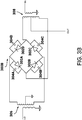
- mixer 300A includes switching elements (e.g., diodes 302A-302D) each in parallel with a respective capacitor (e.g., capacitors 304A-304D, respectively) that form a ring.
- the diodes 302A-302D can be any suitable circuit elements configured to function as a diode, such as semiconductor diodes or diode-connected transistors).
- Capacitors 304A-304D are explicit capacitors rather than parasitic capacitors.
- a "ring" mixer generally refers to a mixer having its mixing elements (typically four elements) arranged in a shape of a ring to mix or modulate an input signal with a carrier signal or local oscillator signal to generate an output signal.
- the IF signal can reduce and/or eliminate a temporal discontinuity during the LO signal crossover time T1 indicated in Figure 2B .
- the linearity (e.g., IIP3) of the mixer 300A can be improved relative to the mixer 200. This improvement can be provided up to a given process technology limit.
- Each capacitor 304A-304D may have a relatively small capacitance, such as a capacitance in a range from 25 fF to 50pF. With such relatively small capacitances, mixing conversion gain reduction from inclusion of capacitors 304A-304D can be constrained, while enabling increases in linearity as described herein.
- the specific capacitance selected for the mixer 300 can be based on a size of the diodes 302A-302D. Additionally, the specific capacitance can be based on the size of the RF to IF balun (e.g., illustrated in Figure 3B ).
- a low noise amplifier may can provide gain (e.g., LNA 104 illustrated in Figure 1A ) so as to compensate for mixer conversion gain lost via utilization of the capacitors 304A-304D. That is, design (e.g., optimization) of diode size and/or the RF-to-IF balun and/or amplifier gain (e.g., low noise amplifier gain) can compensate for possible reduction in conversion gain associated with the capacitors in parallel with respective switching elements in the embodiments of Figures 3A-3E .
- FIG. 3B is a schematic diagram of mixer 300B according to another embodiment. As illustrated, the mixer 300B of Figure 3B includes baluns 306, 308, and the features of the mixer 300A of Figure 3A . For example, local oscillator (LO) balun 306 and an input signal balun 308 are illustrated in combination with the elements of the mixer 300A of Figure 3A .
- LO local oscillator
- Parallel capacitors 304A-304D are coupled in parallel to the signal path, thus improving linearity via enabling a relatively small amount of leakage current to flow during a zero-crossing transition time of the LO signal 312. Accordingly, the LO signal LO and the Input signal IN can be mixed, and an output signal OUT with improved linearity can be tapped off from the input signal balun 308.
- the illustrated input signal IN can be an IF signal or an RF signal.
- the illustrated output signal OUT can be the input signal IN multiplied by the LO signal. Accordingly, the output signal OUT can be frequency shifted relative to the input signal IN.
- the illustrated ports for the input signal IN and the output signal OUT can be switched with each other depending on the application. Accordingly, in certain applications, the signal labeled OUT in Figure 3B can be an input signal, and the signal labeled IN can be an output signal.
- FIG. 3C is a schematic diagram of a mixer 300C according to another embodiment.
- the illustrated mixer 300C includes transistors 332, 334, 336, and 338 implementing switching circuit elements that form a ring.
- Capacitors 340, 342, 344, and 346 are respectively coupled in parallel with the transistors 332-338 between the source and the drain of the respective transistors 332-338.
- the gates of the transistors 332-338 of the mixer ring are coupled to the LO balun 316 at nodes 351, 353, and the mixer ring is coupled to the input signal balun 318 at nodes 359, 361, and an output signal balun 330 at nodes 355, 357.
- the mixer 300C in Figure 3C is implemented with FET transistors (e.g., NFET), the mixer 300C can be any passive H-bridge ring mixer, quad FET mixer, or a FET ring mixer, or other suitable FET-based mixer, which can be implemented, for example, with NFET and/or PFET transistors.
- each transistor can operate as a switch that is either on or off.
- the transistors for a passive mixer can electrically connect two nodes when on and electrically isolate the two nodes when off.
- transistors can be periodically turned on and off to mix signals.
- a passive mixer can be in series with an active circuit and pass DC current of the active circuit.
- the differential LO signal from the LO balun 316 at the nodes 351, 353 can turn different transistors 332-338 of the mixer ring on and off.
- the mixer ring can alternatingly connect the differential input from the input signal balun 318 at the differential input nodes 359, 361 to the differential output nodes 355, 357 of the mixer ring.
- the output signal balun 330 converts or transforms the differential output signals at the nodes 355, 357 to produce the output signal, OUT, which is effectively the input signal, IN, multiplied by the LO signal, LO.
- the mixer 300B can be partially or fully differential, receiving and/or producing differential input, LO, and/or output signals.
- Figure 3D is a schematic diagram of a mixer 300D according to another embodiment.
- the mixer 300D is similar to the mixer 300B, except that it includes transistors 372-378 which are each electrically connected to be a diode connected transistor.
- transistors 372-378 which are each electrically connected to be a diode connected transistor.
- the gate and drain of each transistor can be electrically connected to each other.
- FIG. 3E is a schematic diagram of a mixer 300E according to another embodiment.
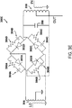
- the mixer 300E of Figure 3E is similar to mixer 300A of Figure 3A , but includes a series combination of a capacitor and a resistor in parallel with each switching element (e.g., diodes 302A-302D). Additionally, the mixer 300E includes baluns, for example local oscillator (LO) balun 306 and input signal balun 308 are illustrated. In some embodiments, the mixer 300E may include a capacitor in parallel with a balun (e.g., capacitor 388 is illustrated in the example of Figure 3E ).
- LO local oscillator
- the series combination of the capacitor and resistor in parallel with each diode can further improve linearity relative to a capacitor in parallel with each diode. While the illustration of Figure 3E includes diodes, it should be understood that the diodes may be replaced with transistors such that each transistor can be in parallel with a respective series combination of a capacitor and resistor.
- diodes 302A-302D are connected in parallel to a respective series combination of capacitors 304A-304D and resistors 386A-386D.
- the illustrated resistors 386A-386D are explicit resistors rather than parasitic resistors.
- a resistance selected or determined for each resistor 386A-386D can be based on features of the mixer 300E, and particular performance characteristics being sought. As an example, a greater resistance may improve linearity but noise performance may be degraded with respect to a smaller resistance. As another example, a smaller resistance may improve noise performance, but degrade conversion loss.
- a capacitor coupled between IF terminals can provide an improvement in linearity relative to the mixer of Figure 2A .
- a capacitor can be coupled between differential ports on an RF-IF side balun of a mixer in combination with any of the features of Figure 3A-3E .
- a series combination of a capacitor and a resistor can be coupled between differential ports on an RF-IF side balun of a mixer in combination with any of the features of Figure 3A-3E .
- a capacitor or a series combination of a capacitor and a resistor can be coupled between differential ports on an RF-IF side balun of a mixer as an alternative to the embodiments of Figures 3A-3E .
- Figure 4 illustrates an example simulation showing linearity improvement over a range of RF signal frequency (e.g., 5 GHz to 9 GHz) for disparate mixers.
- linearity e.g., IP3
- a mixer that includes capacitors in parallel with switching diodes e.g., the mixer 300A of Figure 3A
- just switching diodes e.g., the mixer 200 of Figure 2A
- the graph 410 shows that a mixer with diodes in parallel with a series RC circuit (e.g., the mixer 300E of Figure 3E ) corresponding to the curve 406 has improved linearity relative to the mixers corresponding to the curves 402 and 404.
- the mixer corresponding to the curve 404 in Figure 4 was implemented with 50 fF (femtofarad) capacitors.
- the mixer corresponding to the curve 406 was implemented with 50 fF capacitors and 90 Ohm resistors.
- the IP3 for mixers corresponding to curve 404, 406 is improved relative to IP3 for the mixer corresponding to the curve 402.
- graph 420 illustrates the Pldb linearity improvement over a same frequency range as the graph 410. Similar to the IP3 linearity improvement, the mixers corresponding to curves 404 and 406 have Pldb that is improved relative to the mixer corresponding to the curve 402.
- the mixers disclosed herein can be implemented in a variety of electronic systems.
- the mixers discussed herein can be implemented in a receiver, a transmitter, and/or a transceiver.
- a mixer in accordance with any suitable principles and advantages discussed herein can receive a radio frequency signal from a low noise amplifier and down convert the radio frequency signal using a local oscillator signal from a local oscillator.
- a mixer in accordance with any suitable principles and advantages discussed herein can up convert a signal to radio frequency using a local oscillator signal from a local oscillator. The up converted signal can be provided to a power amplifier, for example.
- Aspects of the disclosure are applicable to any systems and/or devices that could benefit from a mixer with improved linearity.
- aspects of this disclosure can be implemented in various electronic devices. For instance, aspects of this disclosure can be implemented in any electronic device or electronic component that could benefit from a mixer with improved linearity. As an example, aspects of this disclosure can be implemented in any electronic device or electronic component with a transmitter, receiver, or transceiver that could benefit from a mixer with improved linearity.
- Examples of the electronic devices can include, but are not limited to, consumer electronic products, parts of the consumer electronic products, electronic test equipment, vehicular electronics systems, and so on. Examples of the electronic devices can include, but are not limited to, computing devices, communications devices, electronic household appliances, automotive electronics systems, etc. Further, the electronic devices can include unfinished products.
- the words “comprise,” “comprising,” “include,” “including,” and the like are to generally be construed in an inclusive sense, as opposed to an exclusive or exhaustive sense; that is to say, in the sense of "including, but not limited to.”
- the word “coupled,” as generally used herein, refers to two or more elements that may be either directly coupled to each other, or coupled by way of one or more intermediate elements.
- the word “connected,” as generally used herein, refers to two or more elements that may be either directly connected, or connected by way of one or more intermediate elements.
- conditional language used herein such as, among others, “can,” “could,” “might,” “may,” “e.g.,” “for example,” “such as” and the like, unless specifically stated otherwise or otherwise understood within the context as used, is generally intended to convey that certain embodiments include, while other embodiments do not include, certain features, elements and/or states.
- conditional language is not generally intended to imply that features, elements and/or states are in any way required for one or more embodiments or that one or more embodiments necessarily include logic for deciding whether these features, elements and/or states are included or are to be performed in any particular embodiment.
Landscapes
- Engineering & Computer Science (AREA)
- Power Engineering (AREA)
- Computer Networks & Wireless Communication (AREA)
- Signal Processing (AREA)
- Superheterodyne Receivers (AREA)
- Amplifiers (AREA)
- Transmitters (AREA)
Abstract
Description
- Any and all applications for which a foreign or domestic priority claim is identified in the Application Data Sheet as filed with the present application are hereby incorporated by reference in their entirety under 37 CFR 1.57. This application claims the benefit of priority of U.S. Provisional Patent Application No.
US 62/531,226, filed July 11, 2017 - The described technology generated relates to electronics and, more specifically, to mixers.
- Mixers are often used in various circuits such as radio frequency (RF) receivers and transmitters for functions such as down converting or up converting. Generally, for mixers, such as diode ring mixer or field effect transistor (FET) ring mixers, linearity is a significant characteristic that affects, for example, cross modulation, desensitization, harmonic generation, gain compression, and degradation in the signal-to-noise and distortion ratio (SNDR). Due to various inherent non-linear characteristics of mixer elements, such as diodes or transistors, and various other design considerations and trade-offs in mixer design, improving linearity of a mixer can be challenging.
- The innovations described in the claims each have several aspects, no single one of which is solely responsible for its desirable attributes. Without limiting the scope of the claims, some prominent features of this disclosure will now be briefly described.
- In an embodiment, a mixer includes switching circuit elements configured to be switched on and switched off based at least partly on the local oscillator signal. The mixer includes capacitors comprising a respective capacitor in parallel with each of the switching elements. The mixer is configured to mix the input signal with the local oscillator signal to thereby frequency shift the input signal.
- The switching circuit elements can be diodes. The mixer can be a double balanced diode mixer. The switching circuit elements can be field effect transistors. A respective gate can be electrically connected to a respective drain of each field effect transistor of the field effect transistors. The mixer can include resistors arranged such that each of the switching elements is in parallel with a series circuit, the series circuit comprising a capacitor of the capacitors in series with a resistor of the resistors. The mixer can be a passive mixer. The mixer can include an input balun coupled to at least one of the switching circuit elements. The mixer can include an additional capacitor coupled across differential ports of the input balun. The mixer can include an output balun configured to provide the frequency shifted input signal.
- According to an embodiment, a mixer includes diodes configured to switch based at least partly on the local oscillator signal and capacitors, each of which is arranged in parallel with a respective diode of the diodes. The mixer is configured to mix the input signal with the local oscillator signal to thereby frequency shift the input signal.
- The mixer is a double balanced diode mixer. The diodes comprise at least 4 diodes. The mixer includes resistors, each of which is included in a series RC circuit that also includes a capacitor of the capacitors and is in parallel with a diode of the diodes. Each diode is a diode-connected field effect transistor. The mixer includes an input balun coupled to at least one of the diodes.
- According to an embodiment, a method for mixing an input signal with a local oscillator (LO) signal with improved linearity. The method includes receiving, at inputs of a mixer, the input signal and the LO signal; and mixing, with switching elements of the mixer, the input signal and the LO signal to generate a frequency shifted input signal, wherein the switching elements and the capacitors are arranged such that leakage current flows across the switching elements during a zero crossing transition time of the LO signal to improve linearity of the mixer
- The switching elements are arranged in a ring, and each capacitor of the capacitors is in parallel with a respective switching element of the switching elements. The mixer includes a series combination of a capacitor of the capacitors and a resistor in parallel with each of the switching element. The method further comprises providing the input signal to the mixer with an amplifier having a gain arranged to compensate for conversion gain of the mixer.
- The following drawings and the associated description herein are provided to illustrate specific embodiments of the disclosure and are not intended to be limiting.
-
Figure 1A is a diagram of an example implementation of the technology disclosed herein in a receiver according to one embodiment. -
Figure 1B is a diagram of another example implementation of the technology disclosed herein in a transmitter according to one embodiment. -
Figure 2A illustrates switching diodes of an example double balanced mixer. -
Figure 2B illustrates a timing diagram of the LO signal for the example mixer. -
Figure 3A is a schematic diagram of an example mixer according to an embodiment. -
Figure 3B is a schematic diagram of the example mixer according to another embodiment. -
Figure 3C is a schematic diagram of a mixer according to another embodiment. -
Figure 3D is a schematic diagram of a mixer according to another embodiment. -
Figure 3E is a schematic of a mixer according to another embodiment. -
Figure 4 illustrates an example simulation showing linearity improvement for disparate mixers. - Various aspects of the novel systems, apparatuses, and methods are described more fully hereinafter with reference to the accompanying drawings. Aspects of this disclosure may, however, be embodied in many different forms and should not be construed as limited to any specific structure or function presented throughout this disclosure. Rather, these aspects are provided so that this disclosure will be thorough and complete, and will fully convey the scope of the disclosure to those skilled in the art. Based on the teachings herein, one skilled in the art should appreciate that the scope of the disclosure is intended to cover any aspect of the novel systems, apparatuses, and methods disclosed herein, whether implemented independently of or combined with any other aspect. For example, an apparatus may be implemented or a method may be practiced using any number of the aspects set forth herein. In addition, the scope is intended to encompass such an apparatus or method which is practiced using other structure, functionality, or structure and functionality in addition to or other than the various aspects set forth herein. It should be understood that any aspect disclosed herein may be embodied by one or more elements of a claim.
- Although particular aspects are described herein, many variations and permutations of these aspects fall within the scope of the disclosure. Although some benefits and advantages of the preferred aspects are mentioned, the scope of the disclosure is not intended to be limited to particular benefits, uses, or objectives. Rather, aspects of the disclosure are intended to be broadly applicable to any systems and/or devices that could benefit from a mixer with improved linearity. The detailed description and drawings are merely illustrative of the disclosure rather than limiting, the scope of the disclosure being defined by the appended claims and equivalents thereof.
- In this description, reference is made to the drawings where like reference numerals can indicate identical or functionally similar elements. It will be understood that elements illustrated in the figures are not necessarily drawn to scale. Moreover, it will be understood that certain embodiments can include more elements than illustrated in a drawing and/or a subset of the elements illustrated in a drawing. Further, some embodiments can incorporate any suitable combination of features from two or more drawings.
- Mixers are often used in various circuits, such as radio frequency (RF) receivers and transmitters, for functions such as down converting or up converting of signals (e.g., conversion of an RF signal up or down in frequency). Passive mixers can include switching diodes and baluns, and can process local oscillator (LO), radio frequency (RF), and intermediate frequency (IF) signals. The mixers can further include switching elements, such as diodes or transistors (e.g., field effect transistors). In some instances, a turn-on voltage of the switching diodes can be about 0.7 Volts (V). Thus, a LO signal amplitude of 1.4 V or higher can turn on such switching diodes. During the time during which the LO signal is transitioning and less than 1.4 V, the switching diodes may experience no current path, which can cause non-linearity in the mixer due to discontinuity of the IF and RF signals. This disclosure provides technical solutions to improve linearity of such a mixer.
- Commonly, mixers include non-linear elements such as diodes, field effect transistors, and the like. Due to use of these non-linear elements, linearity is a significant characteristic for mixers. Linearity can affect, for example, cross modulation, desensitization, harmonic generation, gain compression, degradation in the signal-to-noise and distortion ratio (SNDR), or any combination thereof. Due to various non-linear characteristics of mixer elements, such as diodes, and various other design considerations and trade-offs in mixer design, improving linearity of a mixer can be challenging.
- Some efforts to linearize a mixer have involved stacking a switching diode in series or adding passive resistors in series with switching diodes. While these may result in linearity gains, such efforts can involve a higher local oscillator (LO) amplitude to turn on switching diodes. These designs can therefore be impractical to implement in various applications. As an example, an application in which lower amplitude signals are commonly utilized such as in cell phone wireless transmissions. Other efforts have involved resistors solely in parallel with switching diodes. These designs may result in higher noise figures, and again may be impractical for particular applications.
- Example mixers with improved linearity are described below, for example in
Figures 3A-3E , with the example mixers including capacitors coupled in parallel with switching elements (e.g., diodes and/or field effect transistors). For example, a relatively small capacitor may be coupled in parallel with each switching diode of a mixer. By adding such a capacitor in parallel with each switching-diode, a relatively small amount of leakage current can flow during a zero-crossing transition time of a local oscillator (LO) signal. Accordingly, this can compensate for a discontinuity issue discussed above, which may be present without capacitors in parallel with switching diodes. With such compensation, linearity characteristic parameters, such as an input 3rd order intercept point (IIP3) and/or an output 3rd order intercept point (OIP3) and/or 1-dB compression point (P1dB), can be improved. An example simulation of such an improvement is illustrated inFigure 4 . -
Figure 1A is a diagram of an example implementation of the technology disclosed herein in areceiver 100A according to one embodiment. The illustratedreceiver 100A includes anantenna 102, a low noise amplifier (LNA) 104, amixer 106, alocal oscillator 108, and anamplifier 110. In certain embodiments, theLNA 104, themixer 106, and theamplifier 110 can be included on a single integrated circuit. A low pass filter may be included between themixer 106 and theamplifier 110. Theantenna 102 and/or thelocal oscillator 108 can be external or internal to the integrated circuit. It will be understood that the receivers and/or the transmitters illustrated inFigures 1A-1B may include fewer or more elements than illustrated. In certain implementations, the receivers and/or transmitters disclosed herein can include additional elements or components, such as baluns or transformers for providing differential or single-ended signals, intermediate frequency (IF) bandpass filters for filtering out unwanted harmonics, etc. As another example, any of the illustrated antennas can be used for both transmitting RF signals and receiving RF signals and a switch can selectively electrically connect a transmit path or a receive path to such an antenna. As described herein, same or corresponding numerals and/or names of elements inFigures 1A-4 and their descriptions indicate the elements having similar or corresponding functionalities and/or characteristics. - The illustrated
receiver 100A can receive an RF signal at theantenna 102, and the RF signal can be provided to theLNA 104. An RF signal can have a frequency in the range from about 30 kHz to 300 GHz, such as in a range from about 450 MHz to about 6 GHz for certain communications standards. TheLNA 104 can amplify the received RF signal and provide the amplified RF signal to themixer 106. Thelocal oscillator 110 can provide a local oscillator signal to themixer 106. In some implementations, thelocal oscillator 108 can provide a differential local oscillator signal to themixer 106. Theamplifier 110 receives a mixer output from themixer 106, and theamplifier 112 may output an amplified IF signal for further processing. - The
mixers 106 illustrated inFigures 1A-1B may be single-ended. In some embodiments, the mixers disclosed herein can be implemented as a partially or fully differential mixer receiving differential signal input, differential LO input, and/or producing differential signal output. In some embodiments, the mixers disclosed herein can be implemented with a passive mixer, ring mixer, H-bridge mixer, unbalanced mixer with a single mixing element, double-balanced mixer, and/or Gilbert cell mixer, for example. In some embodiments, the mixers disclosed herein can be implemented with rectifiers or diodes, such as P-N junction diodes, Schottky barrier diodes, GaAs diodes, semiconductor diodes, or the like. In some embodiments, the mixers disclosed herein can be implemented with field effect transistors (FETs), such as metal oxide semiconductor (MOS) transistors, which can be in complementary form, junction field effect transistors (JFETs), laterally diffused metal oxide semiconductor (LDMOS) transistors, GaAs metal semiconductor field effect transistors (GaAs MESFETs), pseudomorphic high electron mobility transistors (pHEMTs), or the like. While the terms "metal" and "oxide" may be present in for example, MOS, such transistors can have gates made out of materials other than metals, such as polysilicon, and have dielectric oxide regions made from dielectrics other than silicon oxide, such as a high-κ dielectric. According to some other embodiments, mixers implemented in accordance with the principles and advantages discussed herein can be with bipolar transistors, such as SiGe bipolar transistors or GaAs heterojunction bipolar transistors. According to certain embodiments, the capacitors described herein can be on the same die as the switching circuit elements of the mixer. -
Figure 1B is a diagram of another example implementation of the technology disclosed herein in a transmitter according to one embodiment. The illustratedtransmitter 100B includes anamplifier 112, themixer 106, thelocal oscillator 108, apower amplifier 116, and theantenna 102. In certain embodiments, theamplifier 112, themixer 106, and thepower amplifier 116 can be included on an integrated circuit. A band pass filter may be included between themixer 106 and theamplifier 116. Theantenna 102 and thelocal oscillator 108 can be external to or part of the integrated circuit. - The illustrated
transmitter 100B includes theamplifier 112 that receives an IF signal and outputs an amplified IF signal to themixer 106. Thelocal oscillator 108 can provide a local oscillator signal to themixer 106. In some implementations, thelocal oscillator 108 can provide a differential local oscillator signal to themixer 106. Thepower amplifier 116 receives a mixer output from themixer 106, and thepower amplifier 116 provides an amplified RF signal to theantenna 102 to be transmitted. - The
mixers 106 in the illustratedcircuits Figures 1A-1B can be implemented withexample mixers 300A-300E illustrated in, and described in connection with,Figures 3A-3E below. Any suitable combination of the principles and advantages of any ofFigures 3A-3E can be implemented in amixer 106 ofFigure 1A and/orFigure 1B . -
Figure 2A illustrates switching diodes of an example doublebalanced mixer 200. Theexample mixer 200 includesdiodes 202A-202D arranged as a ring modulator. Themixer 200 is configured to receive a local oscillator (LO) signal and an intermediate frequency (IF) signal.Figure 2B , described below, illustrates a timing diagram of the LO signal for themixer 200. -
Figure 2B illustrates a timing diagram of the LO signal for themixer 200. Depending on diode technology, during the cross-over time T1 indicated inFigure 2B , alldiodes 202A-202D of the mixer ofFigure 2A can be turned off. Each of these diodes may have a turn-on voltage Vt. As shown inFigure 2B , the diodes can be off as the LO signal voltage transitions by twice the magnitude of the turn-on voltage Vt of the diodes. Accordingly, the IF signal of themixer 200 can experience a temporal discontinuity, which can degrade linearity (e.g., IIP3) of themixer 200. - Inclusion of capacitors in parallel with the
diodes 202A-202D, or other switching elements (e.g., the field effect transistors ofFigure 3C ), can improve linearity as described below with respect toFigures 3A-4 . Since themixer 200 does not include such parallel capacitors, themixer 200 can have degraded linearity performance compared to the mixers described herein with respect toFigures 3A-3E . -
Figure 3A is a schematic diagram of anexample mixer 300A according to an embodiment. The illustratedmixer 300A is a double balanced mixer. Themixer 300A can frequency translate an input signal by 100s of MHz in certain instances. According to some other instances, themixer 300A can frequency translate an input signal by 1 GHz to 10 GHz. As illustrated,mixer 300A includes switching elements (e.g.,diodes 302A-302D) each in parallel with a respective capacitor (e.g.,capacitors 304A-304D, respectively) that form a ring. Thediodes 302A-302D can be any suitable circuit elements configured to function as a diode, such as semiconductor diodes or diode-connected transistors).Capacitors 304A-304D, as shown inFigures 3A ,3B , and3E , are explicit capacitors rather than parasitic capacitors. As described herein, a "ring" mixer generally refers to a mixer having its mixing elements (typically four elements) arranged in a shape of a ring to mix or modulate an input signal with a carrier signal or local oscillator signal to generate an output signal. As described above, through inclusion of a capacitor in parallel with each diode of themixer 300A, the IF signal can reduce and/or eliminate a temporal discontinuity during the LO signal crossover time T1 indicated inFigure 2B . Accordingly, the linearity (e.g., IIP3) of themixer 300A can be improved relative to themixer 200. This improvement can be provided up to a given process technology limit. - Each
capacitor 304A-304D may have a relatively small capacitance, such as a capacitance in a range from 25 fF to 50pF. With such relatively small capacitances, mixing conversion gain reduction from inclusion ofcapacitors 304A-304D can be constrained, while enabling increases in linearity as described herein. The specific capacitance selected for the mixer 300 can be based on a size of thediodes 302A-302D. Additionally, the specific capacitance can be based on the size of the RF to IF balun (e.g., illustrated inFigure 3B ). A low noise amplifier (LNA) may can provide gain (e.g.,LNA 104 illustrated inFigure 1A ) so as to compensate for mixer conversion gain lost via utilization of thecapacitors 304A-304D. That is, design (e.g., optimization) of diode size and/or the RF-to-IF balun and/or amplifier gain (e.g., low noise amplifier gain) can compensate for possible reduction in conversion gain associated with the capacitors in parallel with respective switching elements in the embodiments ofFigures 3A-3E . -
Figure 3B is a schematic diagram ofmixer 300B according to another embodiment. As illustrated, themixer 300B ofFigure 3B includesbaluns mixer 300A ofFigure 3A . For example, local oscillator (LO)balun 306 and aninput signal balun 308 are illustrated in combination with the elements of themixer 300A ofFigure 3A . -
Parallel capacitors 304A-304D are coupled in parallel to the signal path, thus improving linearity via enabling a relatively small amount of leakage current to flow during a zero-crossing transition time of the LO signal 312. Accordingly, the LO signal LO and the Input signal IN can be mixed, and an output signal OUT with improved linearity can be tapped off from theinput signal balun 308. The illustrated input signal IN can be an IF signal or an RF signal. The illustrated output signal OUT can be the input signal IN multiplied by the LO signal. Accordingly, the output signal OUT can be frequency shifted relative to the input signal IN. The illustrated ports for the input signal IN and the output signal OUT can be switched with each other depending on the application. Accordingly, in certain applications, the signal labeled OUT inFigure 3B can be an input signal, and the signal labeled IN can be an output signal. -
Figure 3C is a schematic diagram of amixer 300C according to another embodiment. The illustratedmixer 300C includestransistors Capacitors Figure 3C , the gates of the transistors 332-338 of the mixer ring are coupled to theLO balun 316 atnodes input signal balun 318 atnodes output signal balun 330 atnodes - Although the illustrated
mixer 300C inFigure 3C is implemented with FET transistors (e.g., NFET), themixer 300C can be any passive H-bridge ring mixer, quad FET mixer, or a FET ring mixer, or other suitable FET-based mixer, which can be implemented, for example, with NFET and/or PFET transistors. In a passive mixer, each transistor can operate as a switch that is either on or off. The transistors for a passive mixer can electrically connect two nodes when on and electrically isolate the two nodes when off. In a passive mixer, transistors can be periodically turned on and off to mix signals. A passive mixer can be in series with an active circuit and pass DC current of the active circuit. The differential LO signal from theLO balun 316 at thenodes input signal balun 318 at thedifferential input nodes differential output nodes output signal balun 330 converts or transforms the differential output signals at thenodes mixer 300B can be partially or fully differential, receiving and/or producing differential input, LO, and/or output signals. -
Figure 3D is a schematic diagram of amixer 300D according to another embodiment. Themixer 300D is similar to themixer 300B, except that it includes transistors 372-378 which are each electrically connected to be a diode connected transistor. For example, the gate and drain of each transistor can be electrically connected to each other. -
Figure 3E is a schematic diagram of amixer 300E according to another embodiment. Themixer 300E ofFigure 3E is similar tomixer 300A ofFigure 3A , but includes a series combination of a capacitor and a resistor in parallel with each switching element (e.g.,diodes 302A-302D). Additionally, themixer 300E includes baluns, for example local oscillator (LO)balun 306 andinput signal balun 308 are illustrated. In some embodiments, themixer 300E may include a capacitor in parallel with a balun (e.g.,capacitor 388 is illustrated in the example ofFigure 3E ). - The series combination of the capacitor and resistor in parallel with each diode can further improve linearity relative to a capacitor in parallel with each diode. While the illustration of
Figure 3E includes diodes, it should be understood that the diodes may be replaced with transistors such that each transistor can be in parallel with a respective series combination of a capacitor and resistor. - As illustrated,
diodes 302A-302D are connected in parallel to a respective series combination ofcapacitors 304A-304D andresistors 386A-386D. The illustratedresistors 386A-386D are explicit resistors rather than parasitic resistors. A resistance selected or determined for eachresistor 386A-386D can be based on features of themixer 300E, and particular performance characteristics being sought. As an example, a greater resistance may improve linearity but noise performance may be degraded with respect to a smaller resistance. As another example, a smaller resistance may improve noise performance, but degrade conversion loss. - With respect to the above-described
Figures 3A-3E , additional variations are possible and fall within the scope of the present disclosure. For example, a capacitor coupled between IF terminals can provide an improvement in linearity relative to the mixer ofFigure 2A . As an example, and as illustrated by thecapacitor 388 inFigure 3E , a capacitor can be coupled between differential ports on an RF-IF side balun of a mixer in combination with any of the features ofFigure 3A-3E . As another example, a series combination of a capacitor and a resistor can be coupled between differential ports on an RF-IF side balun of a mixer in combination with any of the features ofFigure 3A-3E . A capacitor or a series combination of a capacitor and a resistor can be coupled between differential ports on an RF-IF side balun of a mixer as an alternative to the embodiments ofFigures 3A-3E . - Mixers in accordance with the embodiments shown in
Figure 3A-3E have been simulated with various process technologies. The simulations indicate that these embodiments have improved IIP3 by about 6 dBm and also improved output P1dB by +1dB for the process technologies relative to the mixer ofFigure 2A . -
Figure 4 illustrates an example simulation showing linearity improvement over a range of RF signal frequency (e.g., 5 GHz to 9 GHz) for disparate mixers. As illustrated ingraph 410, linearity (e.g., IP3) for a mixer that includes capacitors in parallel with switching diodes (e.g., themixer 300A ofFigure 3A ) corresponding tocurve 404 is improved relative to a mixer with just switching diodes (e.g., themixer 200 ofFigure 2A ) corresponding tocurve 402. Thegraph 410 shows that a mixer with diodes in parallel with a series RC circuit (e.g., themixer 300E ofFigure 3E ) corresponding to thecurve 406 has improved linearity relative to the mixers corresponding to thecurves curve 404 inFigure 4 was implemented with 50 fF (femtofarad) capacitors. The mixer corresponding to thecurve 406 was implemented with 50 fF capacitors and 90 Ohm resistors. - As illustrated, the IP3 for mixers corresponding to
curve curve 402. Additionally,graph 420 illustrates the Pldb linearity improvement over a same frequency range as thegraph 410. Similar to the IP3 linearity improvement, the mixers corresponding tocurves curve 402. - The mixers disclosed herein can be implemented in a variety of electronic systems. For instance, the mixers discussed herein can be implemented in a receiver, a transmitter, and/or a transceiver. As one example, a mixer in accordance with any suitable principles and advantages discussed herein can receive a radio frequency signal from a low noise amplifier and down convert the radio frequency signal using a local oscillator signal from a local oscillator. As another example, a mixer in accordance with any suitable principles and advantages discussed herein can up convert a signal to radio frequency using a local oscillator signal from a local oscillator. The up converted signal can be provided to a power amplifier, for example. Aspects of the disclosure are applicable to any systems and/or devices that could benefit from a mixer with improved linearity.
- Aspects of this disclosure can be implemented in various electronic devices. For instance, aspects of this disclosure can be implemented in any electronic device or electronic component that could benefit from a mixer with improved linearity. As an example, aspects of this disclosure can be implemented in any electronic device or electronic component with a transmitter, receiver, or transceiver that could benefit from a mixer with improved linearity. Examples of the electronic devices can include, but are not limited to, consumer electronic products, parts of the consumer electronic products, electronic test equipment, vehicular electronics systems, and so on. Examples of the electronic devices can include, but are not limited to, computing devices, communications devices, electronic household appliances, automotive electronics systems, etc. Further, the electronic devices can include unfinished products.
- Throughout the description and the claims, the words "comprise," "comprising," "include," "including," and the like are to generally be construed in an inclusive sense, as opposed to an exclusive or exhaustive sense; that is to say, in the sense of "including, but not limited to." The word "coupled," as generally used herein, refers to two or more elements that may be either directly coupled to each other, or coupled by way of one or more intermediate elements. Likewise, the word "connected," as generally used herein, refers to two or more elements that may be either directly connected, or connected by way of one or more intermediate elements. Additionally, the words "herein," "above," "below," and words of similar import, when used in this application, shall refer to this application as a whole and not to any particular portions of this application. Where the context permits, words in the above Detailed Description using the singular or plural may also include the plural or singular, respectively. The word "or" in reference to a list of two or more items, is generally intended to encompass all of the following interpretations of the word: any of the items in the list, all of the items in the list, and any combination of the items in the list.
- Moreover, conditional language used herein, such as, among others, "can," "could," "might," "may," "e.g.," "for example," "such as" and the like, unless specifically stated otherwise or otherwise understood within the context as used, is generally intended to convey that certain embodiments include, while other embodiments do not include, certain features, elements and/or states. Thus, such conditional language is not generally intended to imply that features, elements and/or states are in any way required for one or more embodiments or that one or more embodiments necessarily include logic for deciding whether these features, elements and/or states are included or are to be performed in any particular embodiment.
- While certain embodiments of the inventions have been described, these embodiments have been presented by way of example only, and are not intended to limit the scope of the disclosure. Indeed, the novel methods, apparatus, and systems described herein may be embodied in a variety of other forms; furthermore, various omissions, substitutions and changes in the form of the methods, apparatus, and systems described herein may be made without departing from the spirit of the disclosure. For example, circuit blocks and/or circuit elements described herein may be deleted, moved, added, subdivided, combined, and/or modified. Each of these circuit blocks and/or circuit elements may be implemented in a variety of different ways. The accompanying claims and their equivalents are intended to cover any such forms or modifications as would fall within the scope and spirit of the disclosure.
Claims (15)
- A mixer for mixing an input signal with a local oscillator signal, the mixer comprising:switching circuit elements configured to be switched on and switched off based at least partly on the local oscillator signal; andcapacitors comprising a respective capacitor in parallel with each of the switching elements;wherein the mixer is configured to mix the input signal with the local oscillator signal to thereby frequency shift the input signal.
- The mixer of Claim 1, wherein the switching circuit elements are diodes.
- The mixer of Claim 2, wherein the mixer is a double balanced diode mixer.
- The mixer of any preceding Claim, wherein the switching circuit elements are field effect transistors.
- The mixer of Claim 4, wherein a respective gate is electrically connected to a respective drain of each field effect transistor of the field effect transistors.
- The mixer of any preceding Claim, further comprising resistors arranged such that each of the switching elements is in parallel with a series circuit, the series circuit comprising a capacitor of the capacitors in series with a resistor of the resistors.
- The mixer of any preceding Claim, wherein the mixer is a passive mixer.
- The mixer of any preceding Claim, further comprising an input balun coupled to at least one of the switching circuit elements.
- The mixer of Claim 8, further comprising at least one of:a) an additional capacitor coupled across differential ports of the input balun;b) an output balun configured to provide the frequency shifted input signal.
- A mixer for mixing an input signal with a local oscillator signal, the mixer comprising:diodes configured to switch based at least partly on the local oscillator signal; andcapacitors, each of which is arranged in parallel with a respective diode of the diodes;wherein the mixer is configured to mix the input signal with the local oscillator signal to thereby frequency shift the input signal.
- The mixer of Claim 10, wherein at least one of the following applies:a) the mixer is a double balanced diode mixer;b) the diodes comprise at least 4 diodes;c) each diode is a diode-connected field effect transistor.
- The mixer of Claim 10 or Claim 11, further comprising at least one of:a) resistors, each of which is included in a series RC circuit that also includes a capacitor of the capacitors and is in parallel with a diode of the diodes;b) an input balun coupled to at least one of the diodes.
- A method for mixing an input signal with a local oscillator (LO) signal with improved linearity, the method comprising:receiving, at inputs of a mixer, the input signal and the LO signal; andmixing, with switching elements of the mixer, the input signal and the LO signal to generate a frequency shifted input signal, wherein the switching elements and the capacitors are arranged such that leakage current flows across the switching elements during a zero crossing transition time of the LO signal to improve linearity of the mixer.
- The method of Claim 13, wherein at least one of the following applies:a) the switching elements are arranged in a ring, and each capacitor of the capacitors is in parallel with a respective switching element of the switching elements;b) the mixer includes a series combination of a capacitor of the capacitors and a resistor in parallel with each of the switching element.
- The method of either Claim 13 or Claim 14, further comprising providing the input signal to the mixer with an amplifier having a gain arranged to compensate for conversion gain of the mixer.
Applications Claiming Priority (2)
| Application Number | Priority Date | Filing Date | Title |
|---|---|---|---|
| US201762531226P | 2017-07-11 | 2017-07-11 | |
| US15/835,155 US10541651B2 (en) | 2017-07-11 | 2017-12-07 | Mixers with improved linearity |
Publications (2)
| Publication Number | Publication Date |
|---|---|
| EP3429076A1 true EP3429076A1 (en) | 2019-01-16 |
| EP3429076B1 EP3429076B1 (en) | 2025-03-26 |
Family
ID=62842033
Family Applications (1)
| Application Number | Title | Priority Date | Filing Date |
|---|---|---|---|
| EP18181290.0A Active EP3429076B1 (en) | 2017-07-11 | 2018-07-02 | Mixers with improved linearity |
Country Status (4)
| Country | Link |
|---|---|
| US (1) | US10541651B2 (en) |
| EP (1) | EP3429076B1 (en) |
| CN (1) | CN109245727A (en) |
| TW (1) | TWI743376B (en) |
Cited By (1)
| Publication number | Priority date | Publication date | Assignee | Title |
|---|---|---|---|---|
| CN118074630A (en) * | 2023-12-18 | 2024-05-24 | 成都嘉纳海威科技有限责任公司 | Improved multi-tube parallel structure double-balanced mixer |
Families Citing this family (5)
| Publication number | Priority date | Publication date | Assignee | Title |
|---|---|---|---|---|
| US10901248B1 (en) | 2019-10-16 | 2021-01-26 | Himax Technologies Limited | Voltage amplifier circuit and associated amplifying method for flexible waveform adjustment |
| TWI708238B (en) * | 2019-11-18 | 2020-10-21 | 奇景光電股份有限公司 | Voltage amplifying circuit and associated voltage amplifying method |
| TWI806057B (en) | 2021-05-25 | 2023-06-21 | 立積電子股份有限公司 | Mixer circuit |
| TWI771018B (en) | 2021-05-25 | 2022-07-11 | 立積電子股份有限公司 | Double-balanced mixer |
| FR3166019A1 (en) * | 2024-08-28 | 2026-03-06 | Stmicroelectronics International N.V. | IQ Passive Mixer with Enhanced Conversion Gain |
Citations (3)
| Publication number | Priority date | Publication date | Assignee | Title |
|---|---|---|---|---|
| US4125810A (en) * | 1977-04-08 | 1978-11-14 | Vari-L Company, Inc. | Broadband high frequency baluns and mixer |
| EP0308273A1 (en) * | 1987-09-18 | 1989-03-22 | The Marconi Company Limited | Mixer |
| US7643808B2 (en) * | 2005-07-05 | 2010-01-05 | Stmicroelectronics S.A. | Device and method for mixing circuits |
Family Cites Families (58)
| Publication number | Priority date | Publication date | Assignee | Title |
|---|---|---|---|---|
| US2693533A (en) | 1951-12-04 | 1954-11-02 | Ibm | Mixing circuit |
| US2962675A (en) | 1954-10-01 | 1960-11-29 | Lab For Electronics Inc | Balanced modulator |
| DE2334570B1 (en) | 1973-07-07 | 1975-03-06 | Philips Patentverwaltung | Tunable radio frequency input circuitry for a television receiver |
| JPS558165A (en) * | 1978-07-04 | 1980-01-21 | Alps Electric Co Ltd | Double balance type mixer circuit |
| JPS5884508A (en) * | 1981-11-16 | 1983-05-20 | Matsushita Electric Ind Co Ltd | Double balanced mixer equipment |
| US4601063A (en) | 1985-02-28 | 1986-07-15 | Rca Corporation | Doubly-balanced mixer termination |
| NL8503435A (en) | 1985-12-13 | 1987-07-01 | Philips Nv | UHF AMPLIFIER MIXING CIRCUIT. |
| US4817200A (en) | 1987-02-26 | 1989-03-28 | Hewlett-Packard Company | Tracking YIG tuned filter-mixer |
| US4947062A (en) * | 1988-05-19 | 1990-08-07 | Adams Russell Electronics Co., Inc. | Double balanced mixing |
| US5060298A (en) | 1988-12-09 | 1991-10-22 | Siemens Aktiengesellschaft | Monolithic double balanced mixer with high third order intercept point employing an active distributed balun |
| US5157786A (en) | 1990-08-31 | 1992-10-20 | Thomson Consumer Electronics | Biasing networks for balanced mixers |
| US5361409A (en) | 1991-03-12 | 1994-11-01 | Watkins Johnson Company | FET mixer having transmission line transformer |
| GB2262851B (en) * | 1991-12-24 | 1995-05-10 | Marconi Gec Ltd | R.F. mixer |
| GB2282287B (en) | 1993-09-25 | 1998-01-28 | Nokia Mobile Phones Ltd | A mixer |
| US5551076A (en) * | 1994-09-06 | 1996-08-27 | Motorola, Inc. | Circuit and method of series biasing a single-ended mixer |
| US5854974A (en) * | 1995-04-11 | 1998-12-29 | Watkins Johnson Company | Compensated ring mixers |
| US5697092A (en) * | 1995-12-21 | 1997-12-09 | The Whitaker Corporation | Floating fet mixer |
| JPH10335943A (en) | 1997-05-30 | 1998-12-18 | Mitsumi Electric Co Ltd | Mixer circuit of UP / DOWN converter for CATV |
| US6078802A (en) | 1997-11-18 | 2000-06-20 | Trw Inc. | High linearity active balance mixer |
| US6140849A (en) | 1998-08-07 | 2000-10-31 | Trask; Christopher | Active double-balanced mixer with embedded linearization amplifiers |
| US6205324B1 (en) * | 1999-01-29 | 2001-03-20 | Agilent Technologies Inc. | Broadband double-balanced frequency mixer |
| GB9906047D0 (en) | 1999-03-17 | 1999-05-12 | Secr Defence | Improvements in electromagnetic wave receiver front ends |
| US7072636B2 (en) * | 1999-03-25 | 2006-07-04 | Zenith Electronics Corporation | Printed circuit doubly balanced mixer for upconverter |
| US7013122B2 (en) * | 2000-10-23 | 2006-03-14 | Scientific Components Corporation | Ultra high isolation mixer |
| WO2002084859A1 (en) | 2001-04-18 | 2002-10-24 | Nokia Corporation | Balanced circuit arrangement and method for linearizing such an arrangement |
| US6653885B2 (en) * | 2001-05-03 | 2003-11-25 | Peregrine Semiconductor Corporation | On-chip integrated mixer with balun circuit and method of making the same |
| CA2386477C (en) * | 2001-05-15 | 2004-11-23 | Research In Motion Limited | Feedback compensation detector for a direct conversion transmitter |
| US7095989B2 (en) * | 2001-08-28 | 2006-08-22 | Agilent Technologies, Inc. | Frequency translating devices and frequency translating measurement systems with DC bias added to a mixer diode |
| US7035616B2 (en) | 2002-01-04 | 2006-04-25 | International Business Machines Corporation | Two-stage variable-gain mixer employing shunt feedback |
| US6810241B1 (en) | 2002-01-30 | 2004-10-26 | Northrop Grumman Corporation | Microwave diode mixer |
| US7043220B1 (en) * | 2002-10-11 | 2006-05-09 | Maxim Integrated Products, Inc. | Image-rejection mixer having high linearity and high gain |
| US7102411B2 (en) | 2003-03-06 | 2006-09-05 | Broadcom Corporation | High linearity passive mixer and associated LO buffer |
| EP1469590A1 (en) | 2003-04-17 | 2004-10-20 | STMicroelectronics Belgium N.V. | Up convertor mixer linearisation |
| US7020452B1 (en) | 2003-04-29 | 2006-03-28 | Sirenza Microdevices, Inc. | Actively matched center-tapped marchand balanced mixer |
| KR100483848B1 (en) * | 2003-05-29 | 2005-04-15 | 삼성전자주식회사 | CIRCUITS FOR COMPENSATING DECLINATION OF BALANCED IMPEDANCE DEVICE and CIRCUITS FOR MIXING FREQUENCY |
| US20050191985A1 (en) * | 2004-02-27 | 2005-09-01 | Bos Thomas A. | Diode ring configuration for harmonic diode mixers |
| JP4527469B2 (en) * | 2004-08-20 | 2010-08-18 | 三菱電機株式会社 | Diode mixer |
| CA2524751C (en) * | 2004-10-27 | 2009-12-29 | Synergy Microwave Corporation | Passive reflection mixer |
| DE102007013824B4 (en) * | 2006-03-22 | 2013-10-24 | Denso Corporation | Circuit with a transistor |
| US7509102B2 (en) * | 2006-04-07 | 2009-03-24 | Broadcom Corporation | DAC based switching power amplifier |
| FI20065862A0 (en) | 2006-06-30 | 2006-12-28 | Nokia Corp | Passive multifunction frequency mixer |
| US8036623B2 (en) * | 2007-03-13 | 2011-10-11 | Qualcomm, Incorporated | Wireless receiver with notch filter to reduce effects of transmit signal leakage |
| US20080248776A1 (en) * | 2007-03-30 | 2008-10-09 | Seiichi Banba | High-frequency circuit |
| KR100974574B1 (en) * | 2008-01-16 | 2010-08-06 | 한국과학기술원 | Resistive frequency mixing device and signal processing method using same |
| US8331897B2 (en) | 2008-04-07 | 2012-12-11 | Qualcomm Incorporated | Highly linear embedded filtering passive mixer |
| US8112055B2 (en) * | 2008-06-26 | 2012-02-07 | Intel Corporation | Calibrating receive chain to reduce second order intermodulation distortion |
| TWI365597B (en) * | 2008-09-30 | 2012-06-01 | Univ Nat Taiwan | Miniaturized dual balance wave mixer circuit of tri-wringing wire type circuit construction |
| US8391819B2 (en) * | 2010-02-23 | 2013-03-05 | Texas Instruments Incorporated | Narrow band RF filter circuits, devices and processes using impedance translation |
| JP5476198B2 (en) * | 2010-04-19 | 2014-04-23 | ルネサスエレクトロニクス株式会社 | High frequency switch circuit |
| US8693973B2 (en) | 2011-05-02 | 2014-04-08 | California Institute Of Technology | 670 GHz Schottky diode based subharmonic mixer with CPW circuits and 70 GHz IF |
| JP2013046133A (en) * | 2011-08-23 | 2013-03-04 | Sony Corp | Filter circuit, and radio terminal having filter circuit |
| WO2012167555A1 (en) * | 2011-11-15 | 2012-12-13 | 华为技术有限公司 | Method and apparatus for correcting in-phase and quadrature signals |
| US9130508B1 (en) | 2013-06-28 | 2015-09-08 | Hrl Laboratories, Llc | Shunt resistor and capacitor termination for broadband resistive mixer |
| US9425835B2 (en) * | 2013-08-09 | 2016-08-23 | Broadcom Corporation | Transmitter with reduced counter-intermodulation |
| CN107112959A (en) * | 2014-10-17 | 2017-08-29 | 德克萨斯仪器股份有限公司 | Compensating parameter and pre-distorted signals |
| US9780728B1 (en) * | 2016-03-29 | 2017-10-03 | Peregrine Semiconductor Corporation | Double balanced mixer |
| US9793856B1 (en) * | 2016-04-13 | 2017-10-17 | Analog Devices Global | Mixer with improved linearity |
| CN106156435A (en) * | 2016-07-12 | 2016-11-23 | 成都泰格微电子研究所有限责任公司 | A kind of 2 ~ 4 GHz GaAs passive double balanced mixer chip and methods for designing thereof |
-
2017
- 2017-12-07 US US15/835,155 patent/US10541651B2/en active Active
-
2018
- 2018-07-02 EP EP18181290.0A patent/EP3429076B1/en active Active
- 2018-07-10 TW TW107123832A patent/TWI743376B/en active
- 2018-07-11 CN CN201810753852.6A patent/CN109245727A/en active Pending
Patent Citations (3)
| Publication number | Priority date | Publication date | Assignee | Title |
|---|---|---|---|---|
| US4125810A (en) * | 1977-04-08 | 1978-11-14 | Vari-L Company, Inc. | Broadband high frequency baluns and mixer |
| EP0308273A1 (en) * | 1987-09-18 | 1989-03-22 | The Marconi Company Limited | Mixer |
| US7643808B2 (en) * | 2005-07-05 | 2010-01-05 | Stmicroelectronics S.A. | Device and method for mixing circuits |
Non-Patent Citations (1)
| Title |
|---|
| PUSTOVAROV V Y ET AL: "A BROADBAND TWIN BALANCED MICROWAVE MIXER IN INTEGRATED FORM BASED ON TWO-WIRE TRANSMISSION LINES", TELECOMMUNICATIONS AND RADIO ENGINEERING, SCRIPTA TECHNICA,INC., NEW YORK, NY, US, vol. 41/42, no. 2, 28 February 1987 (1987-02-28), pages 28/29, XP000021397, ISSN: 0040-2508 * |
Cited By (1)
| Publication number | Priority date | Publication date | Assignee | Title |
|---|---|---|---|---|
| CN118074630A (en) * | 2023-12-18 | 2024-05-24 | 成都嘉纳海威科技有限责任公司 | Improved multi-tube parallel structure double-balanced mixer |
Also Published As
| Publication number | Publication date |
|---|---|
| US10541651B2 (en) | 2020-01-21 |
| US20190020312A1 (en) | 2019-01-17 |
| CN109245727A (en) | 2019-01-18 |
| EP3429076B1 (en) | 2025-03-26 |
| TWI743376B (en) | 2021-10-21 |
| TW201918019A (en) | 2019-05-01 |
Similar Documents
| Publication | Publication Date | Title |
|---|---|---|
| US10541651B2 (en) | Mixers with improved linearity | |
| US12034406B2 (en) | RF frequency multiplier without balun | |
| US9712158B1 (en) | Apparatus and methods for biasing radio frequency switches | |
| US7102411B2 (en) | High linearity passive mixer and associated LO buffer | |
| US6847808B2 (en) | Ultra-high linearity RF passive mixer | |
| CA2524751C (en) | Passive reflection mixer | |
| US7277682B2 (en) | RF passive mixer with DC offset tracking and local oscillator DC bias level-shifting network for reducing even-order distortion | |
| EP3200342B1 (en) | Single-ended mixer with reduced loss | |
| US9793856B1 (en) | Mixer with improved linearity | |
| US8050644B1 (en) | Highly linear mixer and method for cancelling FET channel resistance modulation | |
| US20090174460A1 (en) | Method of third-order transconductance cancellation and linear mixer thereof | |
| EP1465334B1 (en) | Passive Mixer | |
| KR20070033352A (en) | Tunable Circuitry for Neutralization of Third-order Modulation | |
| US7113755B2 (en) | Passive mixer with improved linearity | |
| US8624658B1 (en) | Frequency mixer having parallel mixer cores | |
| US7113756B2 (en) | Passive mixer with improved linearity | |
| Hassan et al. | A Compact Ultra-High-Linearity 7-to-20 GHz Passive Mixer Achieving up to 37 dBm IIP3 and 25.1 dBm IP1dB in 45nm CMOS SOI | |
| KR101034125B1 (en) | Manual mixer | |
| US8779834B1 (en) | Multi-LO band switched-core frequency mixer | |
| Sengar et al. | Mixer design | |
| KR100650329B1 (en) | Receiver using vertical bipolar junction transistor implemented with deep enwell CMOS. | |
| Bashir | Design of Integrated Mixer for 5G Radio Transceiver | |
| Krishnamurthi | The new party line: Power-frequency tradeoff in linear BiCMOS passive mixers for cellular base stations | |
| Halonen | Designing of Low Power RF-Receiver Front-end with CMOS Technology |
Legal Events
| Date | Code | Title | Description |
|---|---|---|---|
| PUAI | Public reference made under article 153(3) epc to a published international application that has entered the european phase |
Free format text: ORIGINAL CODE: 0009012 |
|
| STAA | Information on the status of an ep patent application or granted ep patent |
Free format text: STATUS: THE APPLICATION HAS BEEN PUBLISHED |
|
| AK | Designated contracting states |
Kind code of ref document: A1 Designated state(s): AL AT BE BG CH CY CZ DE DK EE ES FI FR GB GR HR HU IE IS IT LI LT LU LV MC MK MT NL NO PL PT RO RS SE SI SK SM TR |
|
| AX | Request for extension of the european patent |
Extension state: BA ME |
|
| STAA | Information on the status of an ep patent application or granted ep patent |
Free format text: STATUS: REQUEST FOR EXAMINATION WAS MADE |
|
| 17P | Request for examination filed |
Effective date: 20190716 |
|
| RBV | Designated contracting states (corrected) |
Designated state(s): AL AT BE BG CH CY CZ DE DK EE ES FI FR GB GR HR HU IE IS IT LI LT LU LV MC MK MT NL NO PL PT RO RS SE SI SK SM TR |
|
| STAA | Information on the status of an ep patent application or granted ep patent |
Free format text: STATUS: EXAMINATION IS IN PROGRESS |
|
| 17Q | First examination report despatched |
Effective date: 20210126 |
|
| RAP3 | Party data changed (applicant data changed or rights of an application transferred) |
Owner name: ANALOG DEVICES, INC. |
|
| GRAP | Despatch of communication of intention to grant a patent |
Free format text: ORIGINAL CODE: EPIDOSNIGR1 |
|
| STAA | Information on the status of an ep patent application or granted ep patent |
Free format text: STATUS: GRANT OF PATENT IS INTENDED |
|
| INTG | Intention to grant announced |
Effective date: 20241021 |
|
| GRAS | Grant fee paid |
Free format text: ORIGINAL CODE: EPIDOSNIGR3 |
|
| GRAA | (expected) grant |
Free format text: ORIGINAL CODE: 0009210 |
|
| STAA | Information on the status of an ep patent application or granted ep patent |
Free format text: STATUS: THE PATENT HAS BEEN GRANTED |
|
| AK | Designated contracting states |
Kind code of ref document: B1 Designated state(s): AL AT BE BG CH CY CZ DE DK EE ES FI FR GB GR HR HU IE IS IT LI LT LU LV MC MK MT NL NO PL PT RO RS SE SI SK SM TR |
|
| REG | Reference to a national code |
Ref country code: GB Ref legal event code: FG4D |
|
| REG | Reference to a national code |
Ref country code: CH Ref legal event code: EP |
|
| REG | Reference to a national code |
Ref country code: DE Ref legal event code: R096 Ref document number: 602018080411 Country of ref document: DE |
|
| REG | Reference to a national code |
Ref country code: IE Ref legal event code: FG4D |
|
| PG25 | Lapsed in a contracting state [announced via postgrant information from national office to epo] |
Ref country code: RS Free format text: LAPSE BECAUSE OF FAILURE TO SUBMIT A TRANSLATION OF THE DESCRIPTION OR TO PAY THE FEE WITHIN THE PRESCRIBED TIME-LIMIT Effective date: 20250626 |
|
| PG25 | Lapsed in a contracting state [announced via postgrant information from national office to epo] |
Ref country code: FI Free format text: LAPSE BECAUSE OF FAILURE TO SUBMIT A TRANSLATION OF THE DESCRIPTION OR TO PAY THE FEE WITHIN THE PRESCRIBED TIME-LIMIT Effective date: 20250326 |
|
| PGFP | Annual fee paid to national office [announced via postgrant information from national office to epo] |
Ref country code: GB Payment date: 20250619 Year of fee payment: 8 |
|
| REG | Reference to a national code |
Ref country code: LT Ref legal event code: MG9D |
|
| PG25 | Lapsed in a contracting state [announced via postgrant information from national office to epo] |
Ref country code: NO Free format text: LAPSE BECAUSE OF FAILURE TO SUBMIT A TRANSLATION OF THE DESCRIPTION OR TO PAY THE FEE WITHIN THE PRESCRIBED TIME-LIMIT Effective date: 20250626 |
|
| PG25 | Lapsed in a contracting state [announced via postgrant information from national office to epo] |
Ref country code: HR Free format text: LAPSE BECAUSE OF FAILURE TO SUBMIT A TRANSLATION OF THE DESCRIPTION OR TO PAY THE FEE WITHIN THE PRESCRIBED TIME-LIMIT Effective date: 20250326 |
|
| PG25 | Lapsed in a contracting state [announced via postgrant information from national office to epo] |
Ref country code: LV Free format text: LAPSE BECAUSE OF FAILURE TO SUBMIT A TRANSLATION OF THE DESCRIPTION OR TO PAY THE FEE WITHIN THE PRESCRIBED TIME-LIMIT Effective date: 20250326 |
|
| PGFP | Annual fee paid to national office [announced via postgrant information from national office to epo] |
Ref country code: FR Payment date: 20250620 Year of fee payment: 8 |
|
| PG25 | Lapsed in a contracting state [announced via postgrant information from national office to epo] |
Ref country code: GR Free format text: LAPSE BECAUSE OF FAILURE TO SUBMIT A TRANSLATION OF THE DESCRIPTION OR TO PAY THE FEE WITHIN THE PRESCRIBED TIME-LIMIT Effective date: 20250627 Ref country code: BG Free format text: LAPSE BECAUSE OF FAILURE TO SUBMIT A TRANSLATION OF THE DESCRIPTION OR TO PAY THE FEE WITHIN THE PRESCRIBED TIME-LIMIT Effective date: 20250326 |
|
| REG | Reference to a national code |
Ref country code: NL Ref legal event code: MP Effective date: 20250326 |
|
| PG25 | Lapsed in a contracting state [announced via postgrant information from national office to epo] |
Ref country code: NL Free format text: LAPSE BECAUSE OF FAILURE TO SUBMIT A TRANSLATION OF THE DESCRIPTION OR TO PAY THE FEE WITHIN THE PRESCRIBED TIME-LIMIT Effective date: 20250326 |
|
| PG25 | Lapsed in a contracting state [announced via postgrant information from national office to epo] |
Ref country code: SE Free format text: LAPSE BECAUSE OF FAILURE TO SUBMIT A TRANSLATION OF THE DESCRIPTION OR TO PAY THE FEE WITHIN THE PRESCRIBED TIME-LIMIT Effective date: 20250326 |
|
| REG | Reference to a national code |
Ref country code: AT Ref legal event code: MK05 Ref document number: 1779978 Country of ref document: AT Kind code of ref document: T Effective date: 20250326 |
|
| PG25 | Lapsed in a contracting state [announced via postgrant information from national office to epo] |
Ref country code: SM Free format text: LAPSE BECAUSE OF FAILURE TO SUBMIT A TRANSLATION OF THE DESCRIPTION OR TO PAY THE FEE WITHIN THE PRESCRIBED TIME-LIMIT Effective date: 20250326 |
|
| PG25 | Lapsed in a contracting state [announced via postgrant information from national office to epo] |
Ref country code: ES Free format text: LAPSE BECAUSE OF FAILURE TO SUBMIT A TRANSLATION OF THE DESCRIPTION OR TO PAY THE FEE WITHIN THE PRESCRIBED TIME-LIMIT Effective date: 20250326 Ref country code: PT Free format text: LAPSE BECAUSE OF FAILURE TO SUBMIT A TRANSLATION OF THE DESCRIPTION OR TO PAY THE FEE WITHIN THE PRESCRIBED TIME-LIMIT Effective date: 20250728 |
|
| PGFP | Annual fee paid to national office [announced via postgrant information from national office to epo] |
Ref country code: DE Payment date: 20250620 Year of fee payment: 8 |
|
| PG25 | Lapsed in a contracting state [announced via postgrant information from national office to epo] |
Ref country code: IT Free format text: LAPSE BECAUSE OF FAILURE TO SUBMIT A TRANSLATION OF THE DESCRIPTION OR TO PAY THE FEE WITHIN THE PRESCRIBED TIME-LIMIT Effective date: 20250326 Ref country code: PL Free format text: LAPSE BECAUSE OF FAILURE TO SUBMIT A TRANSLATION OF THE DESCRIPTION OR TO PAY THE FEE WITHIN THE PRESCRIBED TIME-LIMIT Effective date: 20250326 |
|
| PG25 | Lapsed in a contracting state [announced via postgrant information from national office to epo] |
Ref country code: AT Free format text: LAPSE BECAUSE OF FAILURE TO SUBMIT A TRANSLATION OF THE DESCRIPTION OR TO PAY THE FEE WITHIN THE PRESCRIBED TIME-LIMIT Effective date: 20250326 |
|
| PG25 | Lapsed in a contracting state [announced via postgrant information from national office to epo] |
Ref country code: EE Free format text: LAPSE BECAUSE OF FAILURE TO SUBMIT A TRANSLATION OF THE DESCRIPTION OR TO PAY THE FEE WITHIN THE PRESCRIBED TIME-LIMIT Effective date: 20250326 |
|
| PG25 | Lapsed in a contracting state [announced via postgrant information from national office to epo] |
Ref country code: RO Free format text: LAPSE BECAUSE OF FAILURE TO SUBMIT A TRANSLATION OF THE DESCRIPTION OR TO PAY THE FEE WITHIN THE PRESCRIBED TIME-LIMIT Effective date: 20250326 |
|
| PG25 | Lapsed in a contracting state [announced via postgrant information from national office to epo] |
Ref country code: SK Free format text: LAPSE BECAUSE OF FAILURE TO SUBMIT A TRANSLATION OF THE DESCRIPTION OR TO PAY THE FEE WITHIN THE PRESCRIBED TIME-LIMIT Effective date: 20250326 |
|
| PG25 | Lapsed in a contracting state [announced via postgrant information from national office to epo] |
Ref country code: IS Free format text: LAPSE BECAUSE OF FAILURE TO SUBMIT A TRANSLATION OF THE DESCRIPTION OR TO PAY THE FEE WITHIN THE PRESCRIBED TIME-LIMIT Effective date: 20250726 |
|
| REG | Reference to a national code |
Ref country code: DE Ref legal event code: R097 Ref document number: 602018080411 Country of ref document: DE |
|
| PG25 | Lapsed in a contracting state [announced via postgrant information from national office to epo] |
Ref country code: DK Free format text: LAPSE BECAUSE OF FAILURE TO SUBMIT A TRANSLATION OF THE DESCRIPTION OR TO PAY THE FEE WITHIN THE PRESCRIBED TIME-LIMIT Effective date: 20250326 |
|
| PG25 | Lapsed in a contracting state [announced via postgrant information from national office to epo] |
Ref country code: CZ Free format text: LAPSE BECAUSE OF FAILURE TO SUBMIT A TRANSLATION OF THE DESCRIPTION OR TO PAY THE FEE WITHIN THE PRESCRIBED TIME-LIMIT Effective date: 20250326 |
|
| PLBE | No opposition filed within time limit |
Free format text: ORIGINAL CODE: 0009261 |
|
| STAA | Information on the status of an ep patent application or granted ep patent |
Free format text: STATUS: NO OPPOSITION FILED WITHIN TIME LIMIT |
|
| REG | Reference to a national code |
Ref country code: CH Ref legal event code: L10 Free format text: ST27 STATUS EVENT CODE: U-0-0-L10-L00 (AS PROVIDED BY THE NATIONAL OFFICE) Effective date: 20260211 |
|
| REG | Reference to a national code |
Ref country code: CH Ref legal event code: H13 Free format text: ST27 STATUS EVENT CODE: U-0-0-H10-H13 (AS PROVIDED BY THE NATIONAL OFFICE) Effective date: 20260224 |
|
| 26N | No opposition filed |
Effective date: 20260105 |
|
| PG25 | Lapsed in a contracting state [announced via postgrant information from national office to epo] |
Ref country code: LU Free format text: LAPSE BECAUSE OF NON-PAYMENT OF DUE FEES Effective date: 20250702 |
|
| REG | Reference to a national code |
Ref country code: BE Ref legal event code: MM Effective date: 20250731 |
|
| PG25 | Lapsed in a contracting state [announced via postgrant information from national office to epo] |
Ref country code: BE Free format text: LAPSE BECAUSE OF NON-PAYMENT OF DUE FEES Effective date: 20250731 |
|
| PG25 | Lapsed in a contracting state [announced via postgrant information from national office to epo] |
Ref country code: CH Free format text: LAPSE BECAUSE OF NON-PAYMENT OF DUE FEES Effective date: 20250731 |