EP3429002A1 - Monocrystalline solid electrolyte and method of fabrication - Google Patents
Monocrystalline solid electrolyte and method of fabrication Download PDFInfo
- Publication number
- EP3429002A1 EP3429002A1 EP18189543.4A EP18189543A EP3429002A1 EP 3429002 A1 EP3429002 A1 EP 3429002A1 EP 18189543 A EP18189543 A EP 18189543A EP 3429002 A1 EP3429002 A1 EP 3429002A1
- Authority
- EP
- European Patent Office
- Prior art keywords
- layer
- solid electrolyte
- substrate
- providing
- anode
- Prior art date
- Legal status (The legal status is an assumption and is not a legal conclusion. Google has not performed a legal analysis and makes no representation as to the accuracy of the status listed.)
- Granted
Links
Images

Classifications
-
- H—ELECTRICITY
- H01—ELECTRIC ELEMENTS
- H01M—PROCESSES OR MEANS, e.g. BATTERIES, FOR THE DIRECT CONVERSION OF CHEMICAL ENERGY INTO ELECTRICAL ENERGY
- H01M8/00—Fuel cells; Manufacture thereof
- H01M8/10—Fuel cells with solid electrolytes
- H01M8/12—Fuel cells with solid electrolytes operating at high temperature, e.g. with stabilised ZrO2 electrolyte
- H01M8/124—Fuel cells with solid electrolytes operating at high temperature, e.g. with stabilised ZrO2 electrolyte characterised by the process of manufacturing or by the material of the electrolyte
-
- H—ELECTRICITY
- H01—ELECTRIC ELEMENTS
- H01M—PROCESSES OR MEANS, e.g. BATTERIES, FOR THE DIRECT CONVERSION OF CHEMICAL ENERGY INTO ELECTRICAL ENERGY
- H01M8/00—Fuel cells; Manufacture thereof
- H01M8/10—Fuel cells with solid electrolytes
- H01M8/12—Fuel cells with solid electrolytes operating at high temperature, e.g. with stabilised ZrO2 electrolyte
- H01M8/124—Fuel cells with solid electrolytes operating at high temperature, e.g. with stabilised ZrO2 electrolyte characterised by the process of manufacturing or by the material of the electrolyte
- H01M8/1246—Fuel cells with solid electrolytes operating at high temperature, e.g. with stabilised ZrO2 electrolyte characterised by the process of manufacturing or by the material of the electrolyte the electrolyte consisting of oxides
- H01M8/1253—Fuel cells with solid electrolytes operating at high temperature, e.g. with stabilised ZrO2 electrolyte characterised by the process of manufacturing or by the material of the electrolyte the electrolyte consisting of oxides the electrolyte containing zirconium oxide
-
- G—PHYSICS
- G01—MEASURING; TESTING
- G01N—INVESTIGATING OR ANALYSING MATERIALS BY DETERMINING THEIR CHEMICAL OR PHYSICAL PROPERTIES
- G01N27/00—Investigating or analysing materials by the use of electric, electrochemical, or magnetic means
- G01N27/26—Investigating or analysing materials by the use of electric, electrochemical, or magnetic means by investigating electrochemical variables; by using electrolysis or electrophoresis
- G01N27/403—Cells and electrode assemblies
- G01N27/406—Cells and probes with solid electrolytes
- G01N27/407—Cells and probes with solid electrolytes for investigating or analysing gases
- G01N27/4073—Composition or fabrication of the solid electrolyte
-
- H—ELECTRICITY
- H01—ELECTRIC ELEMENTS
- H01M—PROCESSES OR MEANS, e.g. BATTERIES, FOR THE DIRECT CONVERSION OF CHEMICAL ENERGY INTO ELECTRICAL ENERGY
- H01M10/00—Secondary cells; Manufacture thereof
- H01M10/05—Accumulators with non-aqueous electrolyte
- H01M10/056—Accumulators with non-aqueous electrolyte characterised by the materials used as electrolytes, e.g. mixed inorganic/organic electrolytes
- H01M10/0561—Accumulators with non-aqueous electrolyte characterised by the materials used as electrolytes, e.g. mixed inorganic/organic electrolytes the electrolyte being constituted of inorganic materials only
- H01M10/0562—Solid materials
-
- H—ELECTRICITY
- H01—ELECTRIC ELEMENTS
- H01M—PROCESSES OR MEANS, e.g. BATTERIES, FOR THE DIRECT CONVERSION OF CHEMICAL ENERGY INTO ELECTRICAL ENERGY
- H01M4/00—Electrodes
- H01M4/02—Electrodes composed of, or comprising, active material
- H01M4/04—Processes of manufacture in general
-
- H—ELECTRICITY
- H01—ELECTRIC ELEMENTS
- H01M—PROCESSES OR MEANS, e.g. BATTERIES, FOR THE DIRECT CONVERSION OF CHEMICAL ENERGY INTO ELECTRICAL ENERGY
- H01M4/00—Electrodes
- H01M4/86—Inert electrodes with catalytic activity, e.g. for fuel cells
- H01M4/88—Processes of manufacture
-
- H—ELECTRICITY
- H01—ELECTRIC ELEMENTS
- H01M—PROCESSES OR MEANS, e.g. BATTERIES, FOR THE DIRECT CONVERSION OF CHEMICAL ENERGY INTO ELECTRICAL ENERGY
- H01M8/00—Fuel cells; Manufacture thereof
- H01M8/10—Fuel cells with solid electrolytes
- H01M8/12—Fuel cells with solid electrolytes operating at high temperature, e.g. with stabilised ZrO2 electrolyte
- H01M8/124—Fuel cells with solid electrolytes operating at high temperature, e.g. with stabilised ZrO2 electrolyte characterised by the process of manufacturing or by the material of the electrolyte
- H01M8/1246—Fuel cells with solid electrolytes operating at high temperature, e.g. with stabilised ZrO2 electrolyte characterised by the process of manufacturing or by the material of the electrolyte the electrolyte consisting of oxides
-
- H—ELECTRICITY
- H01—ELECTRIC ELEMENTS
- H01M—PROCESSES OR MEANS, e.g. BATTERIES, FOR THE DIRECT CONVERSION OF CHEMICAL ENERGY INTO ELECTRICAL ENERGY
- H01M8/00—Fuel cells; Manufacture thereof
- H01M8/10—Fuel cells with solid electrolytes
- H01M2008/1095—Fuel cells with polymeric electrolytes
-
- H—ELECTRICITY
- H01—ELECTRIC ELEMENTS
- H01M—PROCESSES OR MEANS, e.g. BATTERIES, FOR THE DIRECT CONVERSION OF CHEMICAL ENERGY INTO ELECTRICAL ENERGY
- H01M8/00—Fuel cells; Manufacture thereof
- H01M8/10—Fuel cells with solid electrolytes
- H01M8/12—Fuel cells with solid electrolytes operating at high temperature, e.g. with stabilised ZrO2 electrolyte
- H01M2008/1293—Fuel cells with solid oxide electrolytes
-
- H—ELECTRICITY
- H01—ELECTRIC ELEMENTS
- H01M—PROCESSES OR MEANS, e.g. BATTERIES, FOR THE DIRECT CONVERSION OF CHEMICAL ENERGY INTO ELECTRICAL ENERGY
- H01M2300/00—Electrolytes
- H01M2300/0017—Non-aqueous electrolytes
- H01M2300/0065—Solid electrolytes
- H01M2300/0068—Solid electrolytes inorganic
-
- H—ELECTRICITY
- H01—ELECTRIC ELEMENTS
- H01M—PROCESSES OR MEANS, e.g. BATTERIES, FOR THE DIRECT CONVERSION OF CHEMICAL ENERGY INTO ELECTRICAL ENERGY
- H01M2300/00—Electrolytes
- H01M2300/0017—Non-aqueous electrolytes
- H01M2300/0065—Solid electrolytes
- H01M2300/0068—Solid electrolytes inorganic
- H01M2300/0071—Oxides
-
- H—ELECTRICITY
- H01—ELECTRIC ELEMENTS
- H01M—PROCESSES OR MEANS, e.g. BATTERIES, FOR THE DIRECT CONVERSION OF CHEMICAL ENERGY INTO ELECTRICAL ENERGY
- H01M2300/00—Electrolytes
- H01M2300/0017—Non-aqueous electrolytes
- H01M2300/0065—Solid electrolytes
- H01M2300/0068—Solid electrolytes inorganic
- H01M2300/0071—Oxides
- H01M2300/0074—Ion conductive at high temperature
-
- H—ELECTRICITY
- H01—ELECTRIC ELEMENTS
- H01M—PROCESSES OR MEANS, e.g. BATTERIES, FOR THE DIRECT CONVERSION OF CHEMICAL ENERGY INTO ELECTRICAL ENERGY
- H01M2300/00—Electrolytes
- H01M2300/0017—Non-aqueous electrolytes
- H01M2300/0065—Solid electrolytes
- H01M2300/0068—Solid electrolytes inorganic
- H01M2300/0071—Oxides
- H01M2300/0074—Ion conductive at high temperature
- H01M2300/0077—Ion conductive at high temperature based on zirconium oxide
-
- H—ELECTRICITY
- H01—ELECTRIC ELEMENTS
- H01M—PROCESSES OR MEANS, e.g. BATTERIES, FOR THE DIRECT CONVERSION OF CHEMICAL ENERGY INTO ELECTRICAL ENERGY
- H01M2300/00—Electrolytes
- H01M2300/0017—Non-aqueous electrolytes
- H01M2300/0065—Solid electrolytes
- H01M2300/0082—Organic polymers
-
- H—ELECTRICITY
- H01—ELECTRIC ELEMENTS
- H01M—PROCESSES OR MEANS, e.g. BATTERIES, FOR THE DIRECT CONVERSION OF CHEMICAL ENERGY INTO ELECTRICAL ENERGY
- H01M2300/00—Electrolytes
- H01M2300/0088—Composites
- H01M2300/0094—Composites in the form of layered products, e.g. coatings
-
- Y—GENERAL TAGGING OF NEW TECHNOLOGICAL DEVELOPMENTS; GENERAL TAGGING OF CROSS-SECTIONAL TECHNOLOGIES SPANNING OVER SEVERAL SECTIONS OF THE IPC; TECHNICAL SUBJECTS COVERED BY FORMER USPC CROSS-REFERENCE ART COLLECTIONS [XRACs] AND DIGESTS
- Y02—TECHNOLOGIES OR APPLICATIONS FOR MITIGATION OR ADAPTATION AGAINST CLIMATE CHANGE
- Y02E—REDUCTION OF GREENHOUSE GAS [GHG] EMISSIONS, RELATED TO ENERGY GENERATION, TRANSMISSION OR DISTRIBUTION
- Y02E60/00—Enabling technologies; Technologies with a potential or indirect contribution to GHG emissions mitigation
- Y02E60/10—Energy storage using batteries
-
- Y—GENERAL TAGGING OF NEW TECHNOLOGICAL DEVELOPMENTS; GENERAL TAGGING OF CROSS-SECTIONAL TECHNOLOGIES SPANNING OVER SEVERAL SECTIONS OF THE IPC; TECHNICAL SUBJECTS COVERED BY FORMER USPC CROSS-REFERENCE ART COLLECTIONS [XRACs] AND DIGESTS
- Y02—TECHNOLOGIES OR APPLICATIONS FOR MITIGATION OR ADAPTATION AGAINST CLIMATE CHANGE
- Y02E—REDUCTION OF GREENHOUSE GAS [GHG] EMISSIONS, RELATED TO ENERGY GENERATION, TRANSMISSION OR DISTRIBUTION
- Y02E60/00—Enabling technologies; Technologies with a potential or indirect contribution to GHG emissions mitigation
- Y02E60/30—Hydrogen technology
- Y02E60/36—Hydrogen production from non-carbon containing sources, e.g. by water electrolysis
-
- Y—GENERAL TAGGING OF NEW TECHNOLOGICAL DEVELOPMENTS; GENERAL TAGGING OF CROSS-SECTIONAL TECHNOLOGIES SPANNING OVER SEVERAL SECTIONS OF THE IPC; TECHNICAL SUBJECTS COVERED BY FORMER USPC CROSS-REFERENCE ART COLLECTIONS [XRACs] AND DIGESTS
- Y02—TECHNOLOGIES OR APPLICATIONS FOR MITIGATION OR ADAPTATION AGAINST CLIMATE CHANGE
- Y02E—REDUCTION OF GREENHOUSE GAS [GHG] EMISSIONS, RELATED TO ENERGY GENERATION, TRANSMISSION OR DISTRIBUTION
- Y02E60/00—Enabling technologies; Technologies with a potential or indirect contribution to GHG emissions mitigation
- Y02E60/30—Hydrogen technology
- Y02E60/50—Fuel cells
-
- Y—GENERAL TAGGING OF NEW TECHNOLOGICAL DEVELOPMENTS; GENERAL TAGGING OF CROSS-SECTIONAL TECHNOLOGIES SPANNING OVER SEVERAL SECTIONS OF THE IPC; TECHNICAL SUBJECTS COVERED BY FORMER USPC CROSS-REFERENCE ART COLLECTIONS [XRACs] AND DIGESTS
- Y02—TECHNOLOGIES OR APPLICATIONS FOR MITIGATION OR ADAPTATION AGAINST CLIMATE CHANGE
- Y02P—CLIMATE CHANGE MITIGATION TECHNOLOGIES IN THE PRODUCTION OR PROCESSING OF GOODS
- Y02P70/00—Climate change mitigation technologies in the production process for final industrial or consumer products
- Y02P70/50—Manufacturing or production processes characterised by the final manufactured product
Definitions
- the present invention generally relates to a fabrication method of layer of solid electrolyte material which is in particular interesting for applications as for instance electrochemical conversion devices or sensors, in particular a solid oxide fuel cell and oxygen sensors.
- the thickness of the solid electrolyte layer has to be chosen with respect to the material quality, in particular in order to avoid electrical shortcuts (for applications for which such a parameter is important) and/or maintain gas tightness which are limiting factors, both of which in particular for SOFC.
- the uniformity of the thickness is highly affected due to the polycrystalline morphology of certain materials commonly used as electrolyte for SOFC.
- the grain size represents a lower limit for the thickness below which the materials properties might change and cannot be guaranteed anymore.
- PVD has normally the advantage that thin films with rather high stoichiometric quality can be produced, but in the context of SOFC the application of PVD is difficult due to the high porosity of the electrode materials acting as growth substrates which is prerequisite of such cells. This impact on material quality influences the already rather low mechanical stability of such PVD solid electrolyte layers. Similar problems are encountered for other thin film deposition techniques as for instance pulsed laser deposition, see for instance Journal of Physics: Conference Series 59, 2007, 140-143 .
- the present invention is not limited to the above depicted cases.
- the present invention is also related to oxygen sensors, in particular like those based on a working principle also called Nernst cell, where a solid electrolyte layer is sandwiched in between two metal electrodes, in particular made of platinum.
- the present invention could also be applicable to other fields, as for instance Li-ion batteries.
- the objective of the invention is to propose a fabrication method of a layer of solid electrolyte material which is in particular interesting for applications as for instance electrochemical conversion devices or sensors, in particular a solid oxide fuel cell and oxygen sensors, obviating the above-mentioned detriments.
- Another objective is to propose a fabrication method of devices and devices comprising such a layer of solid electrolyte.
- applications as for instance Li-ion or Na-ion or H-ion batteries, non-oxygen chemical sensors, air separation units, solid oxide electrolyser cells (SOEC) can be envisaged.
- SOEC solid oxide electrolyser cells
- Further another objective is to propose a structure donor substrate which allows multiple transfer of solid electrolyte material.
- the present invention relates to a method of providing a layer of solid electrolyte by a layer transfer technique from a host substrate.
- the present invention relates to a method of manufacturing a device comprising a solid electrolyte layer, characterized that it comprises providing a host substrate including a crystalline solid electrolyte layer, and transferring said crystalline solid electrolyte layer from the host substrate to a receiver substrate.
- FIG. 1 For brevity, the donor layer of solid electrolyte is provided on the support substrate by a deposition technique, in particular chemical vapor deposition, or, independently, by a second layer transfer technique similar to the one already outlined from another donor substrate.
- a deposition technique in particular chemical vapor deposition, or, independently, by a second layer transfer technique similar to the one already outlined from another donor substrate.
- inventions relate to a method of providing a layer of solid electrolyte wherein the layer transfer technique comprises a step of assembling the host substrate to a receiver substrate, the solid electrolyte layer being between said substrates, and a step of thinning the host substrate.
- step of thinning comprises a step of formation of a zone of weakness in the host substrate so as to define a portion of the host substrate comprising the layer to be transferred and a step of detaching at the zone of weakness so as to transfer said portion to the receiver substrate.
- step of formation of a zone of weakness comprises formation of a release layer in the host substrate, said release layer being activated during the step of detaching in a way that detaching occurs
- Further advantageous embodiments relate to a method of providing a layer of solid electrolyte wherein the detaching step is obtained by at least one of: annealing, application of thermal stress, application of mechanic stress, application of irradiative means, in particular a laser beam, and etching.
- Further advantageous embodiments relate to a method of providing a layer of solid electrolyte wherein the solid electrolyte material has ionic conductivity, in particular for hydrogen, oxygen, lithium or natrium ions, above 0.01 S/cm.
- the present invention allows adaption of the materials properties of the electrolyte layer in order to be able to tune such parameters, for instance the ionic conductivity reaching a certain predetermined value at any wished temperature.
- the ionic conductivity reaching a certain predetermined value at any wished temperature.
- Further advantageous embodiments relate to a method of providing a layer of solid electrolyte wherein the layer of solid electrolyte has a thickness in the range of 10 nm up to 100 ⁇ m with a variation in thickness below 5%, more preferentially below 1%.
- Further advantageous embodiments relate to a method of providing a layer of solid electrolyte wherein the layer of solid electrolyte has a defect density below a predetermined level, in particular lower than 5/cm 2 .
- Further advantageous embodiments relate to a method of providing a layer of solid electrolyte wherein the layer of solid electrolyte is a monocrystalline layer.
- Further advantageous embodiments relate to a method of providing a layer of solid electrolyte wherein the material of the solid electrolyte layer is a perovskite material and/or is chosen among the group of zirconia, ceria, gallates, alumina.
- Further advantageous embodiments relate to a method of providing a layer of solid electrolyte wherein after transfer of the solid electrolyte layer onto the receiver substrate, there remains a portion of the host substrate which is further useable as host substrate for a subsequent transfer of a solid electrolyte layer.
- the present invention also relates to a device, in particular chemical sensor, fuel cell, electrolyser, gas separation unit, or battery, comprising a layer of solid electrolyte obtained by transferring as claimed by the present invention.
- the present invention also relates to a method of fabrication of a solid oxide fuel cell comprising an anode, a cathode, a layer of solid electrolyte in between said anode and cathode, and electrodes on the side of the anode and the cathode opposing to the layer of solid electrolyte, comprising carrying out the method according to the present invention for transferring a crystalline solid electrolyte layer onto the anode and/or the cathode.
- the present invention also relates to a method of fabrication of an oxygen sensor comprising two electrodes and a layer of solid electrolyte in between said two electrodes comprising carrying out the method according to the present invention for transferring a crystalline solid electrolyte layer onto the anode and/or the cathode.
- the present invention also relates to a method of fabrication of a battery comprising an anode, a cathode, a layer of solid electrolyte in between said anode and cathode, and electrodes on the side of the anode and the cathode opposing to the layer of solid electrolyte, comprising carrying out the method according to the present invention for transferring a crystalline solid electrolyte layer onto the anode and/or the cathode.
- the present invention also relates to a method of fabrication of a donor structure comprising a donor substrate having a main surface and a plurality of crystalline solid electrolyte layer portions on said main surface, wherein each of the plurality of crystalline electrolyte layer portions is obtained by the method according to the present invention for transferring a crystalline solid electrolyte layer onto the main surface of the donor substrate.
- This method of fabrication has the advantage that it opens up the way to the possibility to provide high quality solid electrolyte material layers with well defined properties as for instance very good thickness uniformity, high ionic conductivity, and very good electrically insulating properties and that down to very low thickness of the layer.
- the method also gives more flexibility with respect to existing fabrication methods because the materials properties of the transferred layer can be tuned independently, and in particular these properties would not depend on the electrode materials properties (morphology, porosity, defect or dislocation density) as the electrolyte is not directly grown on the electrode.
- the interface properties in particular already improved for molecular or direct bonding, are further enhanced due to the possibility of adapted surface treatments on both the electrode and the electrolyte layer, in particular with respect to the roughness or also the chemical surface termination of these layers.
- FIG. 1A schematically shows a method for providing a layer of solid electrolyte 111 by a layer transfer technique S11 in accordance with embodiments of the present invention. It is schematically indicated that the layer of solid electrolyte 111 is separated from a host substrate 100, thus leaving behind a remaining host substrate 100'. It will become clear from the discussion below regarding various embodiments of the present invention in which way the layer of solid electrolyte 111 may be comprised in the host substrate 100 and in which way the layer of solid electrolyte 111 is separated.
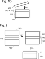
- FIG. 1B schematically shows a host substrate 100 which is entirely formed by a bulk substrate 101. It is also schematically indicated a donor layer of solid electrolyte 110 which is present close to one face of the host substrate 100. It will become clear from the description below in which way such a donor layer of solid electrolyte 110 can be defined in the host substrate 100.
- FIG. 1C schematically shows a host substrate 100 which comprises a support substrate 102 on which is provided a donor layer of solid electrolyte 110.
- a donor layer of solid electrolyte 110 might be obtained by several techniques as for instance, but not limited to, pulsed laser deposition, physical vapour deposition, chemical vapour deposition, spray coating, evaporation, sputtering, or atomic layer deposition.
- the choices of the support substrate 102 as well as the growth technique directly influence the materials properties of the donor layer of solid electrolyte 110 and these properties can be well adjusted depending on the envisaged application.
- FIG. 1D schematically shows a host substrate 100 which comprises a support substrate 202 on which is provided a donor layer of solid electrolyte 210 by a layer transfer technique S11 from a donor substrate 200 as claimed by the present invention.
- This gives the opportunity and flexibility to take into account the preparation of both faces of the layer of solid electrolyte 111, obtained by layer transfer technique in accordance with the present invention from the respective donor layer of solid electrolyte 210, by surface treatments or thermal treatments for which the initial donor substrate would not have been suitable before integration of the layer of solid electrolyte 111 in its final stack of layers or device.
- Materials of choice for the solid electrolyte are doped (dopant X) zirconia-based materials (ZrO 2 -X).
- dopants a large number of divalent and trivalent metal oxides (Y 2 O 3 , Yb 2 O 3 , Sc 2 O 3 , CaO, MgO, etc.) may be selected.
- the monocrystalline phase of such materials is preferred due to higher crystalline quality and lower defect density with respect to the polycrystalline phase.
- the grains of the latter in turn, stabilize the high temperature tetragonal or cubic phase to room temperature.
- tetragonal phase In particular in the ZrO 2 -Y 2 O 3 system, 2.5 mol% Y 2 O 3 stabilizes the tetragonal (t) and 8.5 mol% Y 2 O 3 the cubic (c) phase at 1000°C.
- the tetragonal phase is usually found as a small grain (0.5 pm) material with high mechanical strength, toughness and thermal shock resistance, and an ionic conductivity of 0.055 Scm -1 at 1000°C.
- the large grained cubic phase has lower strength (at RT) but a conductivity of around 0.15 Scm -1 at 1000°C.
- an advantageous embodiment could consist in texturing the material, that is to align the orientation of the grains with respect to the surface which is advantageous because of a better homogeneity of the material, a better control of the thickness uniformity and roughness, as well as a better reproducibility on a manufacturing perspective.
- monocrystalline material is preferably used.
- the thickness should be chosen preferentially higher than the average grain size in order to ensure an overall dense material.
- the present invention is not limited to these kind of materials, and one could envisage other materials as for instance BaY 0,2 Zr 0,8 O 3- ⁇ or doped (CaO, Y 2 O 3 , Sm 2 O 3 , Gd 2 O 3 ) ceria-based materials, in particular Gadolinia-doped ceria, or for instance known perovskite-based lanthanum gallate doped with strontium and magnesium (LSGM).
- ceria-based materials would suffer oxygen loss and need to be protected on the anode side.
- LSGM for instance is incompatible with certain anode materials likely used for SOFC as for instance NiO.
- FIG. 2 schematically shows the assembling step S2 of host substrate 100 comprising a donor layer of solid electrolyte 110 with a receiver substrate 203 and a step of thinning S3 of the assembled structure leading to a layer of solid electrolyte 111 remaining on the receiver substrate 203.
- the assembling step S2 can be obtained by any bonding technique as for instance direct bonding, thermocompression bonding, eutectic bonding, ceramic mediated bonding, or any other known technique suitable.
- a direct bonding is preferred as it provides long term stability of the bond and a defect free bonding interface showing good electrochemical behavior, in particular high ionic conductivity and low electrical conductivity.
- the surface of the receiver substrate 203 as well as the donor layer of solid electrolyte 110 may be prepared, for instance by a step of, or a combination of steps of etching, grinding, polishing, in particular chemical mechanical polishing, or any other surface treatment technique, or even thermal treatment, in order to decrease the roughness of the surface and/or the number of defects present at the surface.
- the thinning step S3 schematically displayed in Figure 2 might be obtained by several techniques some of which will be described below in more detail.
- the step of thinning S3 might be obtained by a combination of grinding and subsequent etching of the host substrate 100 which might be interesting if the material of the host substrate 100 is rather cheap and highly available so that such a sacrificial step would be cost efficient with respect to industrialization.
- Other possibilities of the step of thinning S3 might be the fracture along a zone of weakness 320, for instance obtained by implantation of ionic and/or atomic species or for instance obtained by the introduction of a buried liftoff layer 330 selectively sensitive to etching, defining thus a donor layer of solid electrolyte 110 which can be transferred to the receiver substrate 203.
- Other possibilities of the step of assembling S2 might be providing the receiver substrate 203 by a deposition sequence whereby any technique of deposition, like vapor phase or liquid phase deposition, sputtering, evaporation, spray deposition, spin coating for instance.
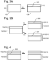
- Figure 3A schematically refers to the case shown in Figure 1B of a host substrate 100 formed entirely by a bulk substrate 101, and shows the step of formation S4 of a zone of weakness 320 by implantation of ionic and/or atomic species, in particular H or He or a combination thereof, through one face of the host substrate 100, thereby defining the donor layer of solid electrolyte 110.
- FIG 3B similar technical aspects are schematically shown which, however, refer to the cases shown in Figures 1C and 1D where a donor layer of solid electrolyte 110 or 210 is provided on a host substrate 102 or 202, respectively.
- the zone of weakness 320 can be either formed in the donor layer of solid electrolyte 110 or 210 or in the support substrate 102 or 202, or in-between in an intermediate layer.
- implantation is realized in a range of implantation energies from 50 keV to 1 MeV with an implantation dose ranging typically from 2x10 16 to 12x10 17 H+/cm 2 in case of H+ ions (and/or He ions) which permits to define a zone of weakness 320 at a depth of about 0.2 to 10 ⁇ m below the implanted surface.
- Figure 4 schematically shows another advantageous embodiment with respect to the step of thinning S3 depicted in Figure 2 .
- Figure 4 shows a host substrate 100 comprising a support substrate 102 or 202 and a donor layer of solid electrolyte 110 or 210, in between of which a release layer, often also called liftoff layer, 330 is formed which acts as a zone of weakness 320 for the step of thinning S3.
- Such a liftoff layer 330 might be introduced either during the growth of the donor layer of solid electrolyte 110 on the support substrate as described with regard to the embodiment schematically shown in Figure 1C , or during the layer transfer technique S11 as schematically shown in Figure 1D whereby the liftoff layer 330 is provided on the support substrate or the layer to be transferred prior to the transfer, or a combination thereof.
- the step of thinning S3 with respect to the formed zone of weakness 320 can be performed by annealing or by application of thermal and/or mechanical stress, for instance a thermal treatment realized in the range of 200°C to 900 °C for a duration ranging from seconds to hours might induce fracture at the zone of weakness 320, allowing thus a step of detachment S5 to occur.
- the insertion of a blade can act as application of mechanical stress.
- Other possibilities might be a step of detaching S5 by application of irradiative means, in particular a laser beam.
- the step of detaching S5 is the application of a selective etch solution to the zone of weakness, easily achievable by an adequate choice of material for the liftoff layer 330 for instance.
- the main advantage of the layer transfer technique S11 involving a step S4 of formation of a zone of weakness and a detaching step S5 is the possibility to reuse the remaining host substrate 100' for further fabrication. This is especially noteworthy whenever the cost of such substrates is rather high. After a rather simple surface treatment, for instance chemical mechanical polishing but not limited to it, of the remaining host substrate 100' the latter can be reused as host substrate 100 or support substrate 102 according to the present invention. However one can also imagine a scenario in which the material of the host substrate 100 is rather cheap, and reuse is not of real economic interest. In such a configuration the thinning step S3 can be equivalent to the removal of the host substrate by any conventional thinning technique (etching, grinding, or polishing).
- Another embodiment is related to the use of an intermediate handling substrate. From the host substrate 100 the layer of solid electrolyte 111 is transferred to an intermediate handling substrate which itself can act subsequently as new host substrate. This is schematically indicated in Figure 1D .
- This is advantageous whenever for instance the crystallographic termination of the layer of solid electrolyte 111 is different on both sides of said layer which might play a role.
- a transfer from the intermediate handling substrate to the receiver substrate 203 does thus not change such termination or orientation, allowing further optimization and giving much more flexibility in the materials choice.
- Other reasons can justify the use of an intermediate handling substrate. For instance, as it allows to de-correlate the step of detaching the electrolyte layer from its original host substrate and the step of assembling it on the final support substrate, more flexible process windows can be obtained. Another reason would be to allow for more flexibility regarding surface treatments of the electrolyte layer, and this for both of its two faces.
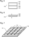
- FIG. 5 schematically illustrates an electrochemical conversion device 510 comprising contact structures 503, an anode 501, a cathode 502, and a layer of solid electrolyte 111 arranged in between said anode 501 and cathode 502.
- the electrochemical conversion device 510 is not limited to the application of SOFC wherein a layer of solid electrolyte 111 is used, but may also be related to similar systems as for instance Li-ion batteries.
- the contact structures 503 not only provide electronic conduction but also comprise means of transport of gas from fuel, whereas in Li-ion batteries essentially electronic conduction is necessary as the ions are transported from anode to cathode and intercalated therein and vice-versa due to the electrochemical potential difference but no reduction or oxidation process occurs leading to or using volatile species as oxygen or hydrogen.
- the materials involved are chosen appropriately.
- the anode materials might be chosen among porous Ni-YSZ cermet, Cu-YSZ cermet, strontium titanate or others commonly known
- cathode materials might be chosen among perovskite-based LaMnO3 accompanied by a ceria-based interlayer to assure chemical stability versus YSZ electrolyte material.
- LSM La 0.8 Sr 0.2 MnO 3
- LSCF La 0.5 Sr 0.5 CoO 3
- BSCF Ba 1-x Sr x Co 1-y Fe y O 3- ⁇
- the solid electrolyte material of choice is LiPON or Li 3 PO 4
- anode and cathode materials might be chosen of those well known in the art, as for instance LiCO 2 , Li, TiOS.
- the process starts by providing the anode 501 by commonly known techniques as for instance sintering.
- the anode is supplied with its electrode already formed, or the corresponding electrode can be formed later in the process.
- a planarization step is performed on the anode 501 in order to provide a surface having low roughness, in particular below 0.6nm rms as measured by Atomic Force Microscopy (AFM), which is much more suitable for the assembling step via bonding techniques.
- AFM Atomic Force Microscopy
- the host substrate 100 from which the layer of solid electrolyte 111 is obtained is made of YSZ in a monocrystalline phase, for instance of square form with dimensions of 20 x 20 mm.
- Implantation of hydrogen H+ is performed on the monocrystalline YSZ in order to obtain the zone of weakness 320 necessary for a subsequent transfer by splitting.
- implantation is performed using implantation energies ranging from 50 keV to 1 MeV, implantation doses ranging from 2 E+16/cm 2 to 1.2E+17/cm 2 , which lead to a zone of weakness 320 separating the donor layer of solid electrolyte 110 having a thickness, which thus depends on the exact implantation parameters, ranging from 0.2 to 10 ⁇ m.
- splitting at the zone of weakness 320 is provided by a thermal treatment with temperatures ranging from 300°C to 1000°C for a duration ranging from seconds to hours depending on the temperature of the anneal.
- an optional planarization step on the transferred layer might be suitable for the subsequent providing of the cathode 502.
- the LSM cathode material might be directly deposited on the transferred layer by any known deposition means, like tape casting, sintering, vapor phase or liquid phase deposition, sputtering, evaporation, sintering, spray coating, sol-gel technique, serigraphy etc., or one could assemble with a separately provided cathode by above mentioned bonding and/or transfer techniques applied to the cathode. For instance assembly could be obtained by lamination or direct bonding of a LSM substrate on the above mentioned planarized YSZ layer which has been transferred on the anode according to embodiments of the present invention.
- a thermal treatment with temperatures ranging from 500°C to 1400°C with a duration ranging from seconds to hours depending on the temperature of the anneal can optionally be performed in order to increase the overall mechanical stability of the assembled structure.
- metal electrodes are provided on both anode (if not already formed) and cathode side by techniques commonly known.
- the method of providing a layer of solid electrolyte 111 according to embodiments of the present invention has the advantage that said method can be used to avoid incompatibilities of the material chosen for the layer of solid electrolyte 111 and the materials chosen for the anode 501 or cathode 502.
- anode 501 and cathode 502 have a certain type of material and morphology, for instance a high porosity, in order to allow optimized performance in the chosen application.
- high porosity is chosen in case of SOFC in order to allow penetration of oxygen or hydrogen in the respective material layer, and also to increase the ionic conductivity of the respective ions to the layer of electrolyte material.
- SOFC in order to allow penetration of oxygen or hydrogen in the respective material layer
- ionic conductivity of the respective ions to the layer of electrolyte material.
- such a rather inhomogeneous morphology negatively impacts layers that would have been grown upon such anode or cathode material and, thus, does not allow high quality, for instance monocrystallinity, and low defect densities as claimed by the present invention.
- the flexibility in the fabrication method of such electrochemical conversion devices 510 is increased as the layer of solid electrolyte 111 may be provided on either the anode 501 or the cathode 502.
- the layer of solid electrolyte 111 and the other structure may undergo treatments in order to improve the interface after assembly, as for instance polishing in order to decrease the roughness, making it more suitable for instance for a bonding process, in particular direct bonding. Further it is also possible to provide bonding layers and/or planarizing layers before assembly on the layer of solid electrolyte 111 and/or the other structure in order to provide better bonding quality.
- the layer of solid electrolyte 111 may be provided on the anode 501, but similar reasoning would apply to a provision on the cathode 502.
- Thermal treatments after or during the assembly might be necessary in order to ensure the mechanical integrity of the assembled structure, with temperature ranging from 500°C up to 1400°C and treatment duration ranging from seconds to hours depending on the temperature of the anneal. Subsequently one has either the choice to assemble a structure comprising the cathode 502 and its contact structure 503 to the free face of the layer of solid electrolyte 111.
- each of the constituent parts of the electrochemical conversion device 510 can be subjected to its proper individual treatment, for instance thermal annealing, chemical treatment, diffusion doping, prior to the assembling with the other constituent parts of the electrochemical conversion device 510.
- Anode 501 and cathode 502 for instance can thus be optimized in terms of catalytic activity for oxygen dissociation and incorporation reactions in cathode 502 and for electrochemical oxidation of H 2 or CO and other fuel processing in anode 501. Further the electronic conductivity of both anode 501 and cathode 502 may be increased due to the flexibility in treatments; the same applies to the chemical and mechanical stability with respect to the other constituents. For instance an alignment of CTE (coefficient of thermal expansion) throughout the electrochemical conversion device 510 might be of interest in order to increase the mechanical stability and, thus, lifetime of the device at the high operating temperature. Such an attunement of CTE might be obtained by the choice of the material. Thus an overall optimized device is obtained.
- CTE coefficient of thermal expansion
- the present invention is related to applications involving a layer of solid electrolyte, as for instance SOFC which is related to generate electricity (and heat) by the input of combustibles or fuels like for instance hydrogen and oxygen.
- SOFC solid oxide electrolyzer cells
- protonic (H+ ion) conduction can be use instead or oxygen ions conduction.
- PEMFC Proton exchange membrane fuel cells
- the present invention can be applied to such protonic systems too, where the protonic membrane is obtained by a layer transfer technique from a host substrate, instead of for instance using an already formed polymer membrane.
- Membranes of solid oxide electrolyte can also be used for gas separation, like oxygen gas separation or hydrogen gas separation. In these cases, it may be necessary that the electrolyte not only allows for ionic conduction through the membrane but also for opposite charge carrier conduction like electrons or holes. Choice of the materials for the membrane depends on the targeted gas species. In the case of oxygen for instance perovskites are frequently used, like Sr 0.8 La 0.2 Fe 0.2 Co 0.8 O 3- ⁇ , SrCo 0.8 Fe 0.2 O 3- ⁇ or Sr 0.5 Ba 0.5 Co 0.8 Fe 0.2 O 3- ⁇ .
- Other materials like SrCe0 3 , BaCe0 3 , CaZr0 3 , SrZr0 3 can also be used.
- one of the main challenges is to increase in a controlled way the conductivity of the membrane, pushing towards thinner and more uniform and denser layers.
- such membranes can be found in Air Separation Units for pure oxygen gas extraction from ambient air, in natural gas refining where CO 2 is removed after hydrogen extraction, and in many others.
- FIG. 6 schematically shows how a solid electrolyte can be used in a chemical sensor, like an oxygen sensor.
- a chemical sensor like an oxygen sensor.
- oxygen sensors may serve for instance to accurately define the air/fuel ratio in order to optimize the control of motor combustion efficiency. They may be placed in the exhaust system or earlier in the chain before the combustion chamber.
- ion conducting materials Based on the utilization of ion conducting materials, several different principles do exist as to the working mechanisms of such sensors. One of them is based on the Nernst effect where an electrical potential is created across the sensor when there is a Oxygen Pressure (pO 2 ) gradient.
- pO 2 Oxygen Pressure
- the layer of solid electrolyte 111 there are contact structures 603 provided, using for instance well-known techniques and materials suitable for this sort of application.
- the air tightness of the layer of electrolyte 111 is important and might be tuned by the layer transfer technique of our present invention as said layer could be prepared in high quality on substrates else than made of the material of the contact structures 603.
- the latter however need certain porosity for gas in order to allow contact with the layer of solid electrolyte 111.
- a reference chamber of known oxygen content and pressure may be used on one side of the sensor.
- a second type of oxygen sensor does measure the variation of the conductivity of the ceramic as a function of the Oxygen pressure (pO 2 ).
- FIG. 7 schematically illustrates one advantageous embodiment, an advanced structured donor substrate, that is a donor structure 701 comprising multiple donor layer of solid electrolyte 110 assembled to the main surface of a large scale donor substrate 700 with a size large enough to accommodate multiple donor layers of solid electrolyte 110.
- a donor structure, or structured donor substrate, 701 is advantageous for large scale applications as a series connection of multiple SOFC in a final SOFC module.
- a high density of donor layers of solid electrolyte 110 can be easily obtained, the providing of the donor layers of solid electrolyte 110 on the donor substrate 700 can thereby be obtained by one of the techniques explained with respect to the present invention, or by application of ceramic glue or other suitable adhesive materials as for instance polymer based materials.
- One multiple transfer of layers of solid electrolyte 111 from a single structured donor substrate 701 as shown in Figure 7 on a receiver substrate 203 of at least the same size offers the possibility to easily integrate SOFC fabrication in an industrially viable environment, with the possibility to process in parallel large areas of electrolyte membranes.
- YSZ in particular monocrystalline YSZ
- Other solid electrolyte material may be considered depending on the application and on the species to be selectively transported through the electrolyte.
- Li-ion or or Na-ion conductivity may be exploited too.
- NaS batteries usually use ⁇ -Alumina for the solid electrolyte material.
- An alternative to the realization of such material by deposition is to use layer transfer techniques described in the present invention, based on the hypothesis that monocrystalline or high quality polycrystalline donor material are also developed separately. The same holds for Li-ion batteries, with solid electrolyte materials like LiPON or Li 3 PO 4 .
- Other famous electrolyte materials, of interest here are Na 3 Zr 2 Si 2 PO 12 (NaSiCON), Na 2 CO 3 and Agl.
Landscapes
- Engineering & Computer Science (AREA)
- Manufacturing & Machinery (AREA)
- Chemical & Material Sciences (AREA)
- Chemical Kinetics & Catalysis (AREA)
- Electrochemistry (AREA)
- General Chemical & Material Sciences (AREA)
- Life Sciences & Earth Sciences (AREA)
- Sustainable Development (AREA)
- Sustainable Energy (AREA)
- Health & Medical Sciences (AREA)
- General Physics & Mathematics (AREA)
- Physics & Mathematics (AREA)
- Analytical Chemistry (AREA)
- Biochemistry (AREA)
- General Health & Medical Sciences (AREA)
- Molecular Biology (AREA)
- Immunology (AREA)
- Pathology (AREA)
- Condensed Matter Physics & Semiconductors (AREA)
- Inorganic Chemistry (AREA)
- Fuel Cell (AREA)
- Conductive Materials (AREA)
- Electrolytic Production Of Non-Metals, Compounds, Apparatuses Therefor (AREA)
- Secondary Cells (AREA)
Abstract
Description
- The present invention generally relates to a fabrication method of layer of solid electrolyte material which is in particular interesting for applications as for instance electrochemical conversion devices or sensors, in particular a solid oxide fuel cell and oxygen sensors.
- General concerns about global warming have initiated many studies in order to find alternative solutions with respect to the utilization of fossil fuels, one of which has been the development of the so called solid oxide fuel cell (SOFC). Industrial scale production of high power fuel cells remains uncertain essentially due to the high production costs and limited life time of these devices. The high production costs are due to time consuming manufacturing techniques while limited life time is linked to the high working temperature of the cells. Such high working temperatures are necessary in order to achieve high ionic conductivity of the materials used as solid electrolyte as the ionic conductivity is a temperature dependent materials parameter. The main actual trends in research are directed to the developments of solid electrolyte layers with higher ionic conductivity and/or lower thickness in order to be able to reduce the working temperature of the cells. However, the thickness of the solid electrolyte layer has to be chosen with respect to the material quality, in particular in order to avoid electrical shortcuts (for applications for which such a parameter is important) and/or maintain gas tightness which are limiting factors, both of which in particular for SOFC. Further for low thickness the uniformity of the thickness is highly affected due to the polycrystalline morphology of certain materials commonly used as electrolyte for SOFC. The grain size represents a lower limit for the thickness below which the materials properties might change and cannot be guaranteed anymore.
- A recent review published in Advances in Manufacturing, Vol. 2, Issue 3, pp 212-221, describes recent efforts obtained using thermal spray techniques and physical vapour deposition (PVD) techniques for SOFC electrolyte layer manufacturing.
- For what concerns thermal spraying, developments have been made with regards to the spraying parameters as well as post processing of the deposited layers but none of these developments were able to provide solid electrolyte layers with a thickness below 10 µm nor has been able to achieve high ionic conductivity compared to high quality bulk material, as for example for yttria stabilized zirconia (YSZ).
- PVD has normally the advantage that thin films with rather high stoichiometric quality can be produced, but in the context of SOFC the application of PVD is difficult due to the high porosity of the electrode materials acting as growth substrates which is prerequisite of such cells. This impact on material quality influences the already rather low mechanical stability of such PVD solid electrolyte layers. Similar problems are encountered for other thin film deposition techniques as for instance pulsed laser deposition, see for instance Journal of Physics: Conference Series 59, 2007, 140-143. Large area deposition of YSZ films with thickness in the range of 300 nm up to 1200 nm have been obtained over areas as large as 50-100 cm2, but such results are only possible on non-porous substrates, for example Si in case of YSZ layers deposited by pulsed layer deposition.
- The above mentioned problems apply to all applications which would involve an electrolyte material in solid form and, thus, the present invention is not limited to the above depicted cases. For instance, the present invention is also related to oxygen sensors, in particular like those based on a working principle also called Nernst cell, where a solid electrolyte layer is sandwiched in between two metal electrodes, in particular made of platinum. The present invention could also be applicable to other fields, as for instance Li-ion batteries.
- The objective of the invention is to propose a fabrication method of a layer of solid electrolyte material which is in particular interesting for applications as for instance electrochemical conversion devices or sensors, in particular a solid oxide fuel cell and oxygen sensors, obviating the above-mentioned detriments. Another objective is to propose a fabrication method of devices and devices comprising such a layer of solid electrolyte. In particular, applications as for instance Li-ion or Na-ion or H-ion batteries, non-oxygen chemical sensors, air separation units, solid oxide electrolyser cells (SOEC) can be envisaged. Further another objective is to propose a structure donor substrate which allows multiple transfer of solid electrolyte material.
- The present invention relates to a method of providing a layer of solid electrolyte by a layer transfer technique from a host substrate.
- In particular the present invention relates to a method of manufacturing a device comprising a solid electrolyte layer, characterized that it comprises providing a host substrate including a crystalline solid electrolyte layer, and transferring said crystalline solid electrolyte layer from the host substrate to a receiver substrate.
- Further advantageous embodiments relate to a method of providing a layer of solid electrolyte characterized in that the host substrate comprises either a bulk substrate of crystalline solid electrolyte material or a donor layer of crystalline solid electrolyte provided on a support substrate.
- Further advantageous embodiments relate to a method of providing a layer of solid electrolyte characterized in that the donor layer of solid electrolyte is provided on the support substrate by a deposition technique, in particular chemical vapor deposition, or, independently, by a second layer transfer technique similar to the one already outlined from another donor substrate.
- Further advantageous embodiments relate to a method of providing a layer of solid electrolyte wherein the layer transfer technique comprises a step of assembling the host substrate to a receiver substrate, the solid electrolyte layer being between said substrates, and a step of thinning the host substrate.
- Further advantageous embodiments relate to a method of providing a layer of solid electrolyte wherein the step of thinning comprises a step of formation of a zone of weakness in the host substrate so as to define a portion of the host substrate comprising the layer to be transferred and a step of detaching at the zone of weakness so as to transfer said portion to the receiver substrate.
- Further advantageous embodiments relate to a method of providing a layer of solid electrolyte wherein the step of formation of a zone of weakness is obtained by implantation of atomic and/or ionic species.
- Further advantageous embodiments relate to a method of providing a layer of solid electrolyte wherein the step of formation of a zone of weakness comprises formation of a release layer in the host substrate, said release layer being activated during the step of detaching in a way that detaching occurs
- Further advantageous embodiments relate to a method of providing a layer of solid electrolyte wherein the detaching step is obtained by at least one of:
annealing, application of thermal stress, application of mechanic stress, application of irradiative means, in particular a laser beam, and etching. - Further advantageous embodiments relate to a method of providing a layer of solid electrolyte wherein the solid electrolyte material has ionic conductivity, in particular for hydrogen, oxygen, lithium or natrium ions, above 0.01 S/cm.
- This is particularly advantageous in order to be able to decrease the operating temperature of certain device applications as for instance SOFC, as the ionic conductivity is a temperature dependent parameter. The present invention allows adaption of the materials properties of the electrolyte layer in order to be able to tune such parameters, for instance the ionic conductivity reaching a certain predetermined value at any wished temperature. Thus even at operating temperature below 600°C, more preferentially below 450°C, one is able to obtain high ionic conductivity of above 0,01 S/cm.
- Further advantageous embodiments relate to a method of providing a layer of solid electrolyte wherein the layer of solid electrolyte has a thickness in the range of 10 nm up to 100 µm with a variation in thickness below 5%, more preferentially below 1%.
- Further advantageous embodiments relate to a method of providing a layer of solid electrolyte wherein the layer of solid electrolyte has a defect density below a predetermined level, in particular lower than 5/cm2.
- Further advantageous embodiments relate to a method of providing a layer of solid electrolyte wherein the layer of solid electrolyte is a monocrystalline layer.
- Further advantageous embodiments relate to a method of providing a layer of solid electrolyte wherein the material of the solid electrolyte layer is a perovskite material and/or is chosen among the group of zirconia, ceria, gallates, alumina.
- Further advantageous embodiments relate to a method of providing a layer of solid electrolyte wherein after transfer of the solid electrolyte layer onto the receiver substrate, there remains a portion of the host substrate which is further useable as host substrate for a subsequent transfer of a solid electrolyte layer.
- Further the present invention also relates to a device, in particular chemical sensor, fuel cell, electrolyser, gas separation unit, or battery, comprising a layer of solid electrolyte obtained by transferring as claimed by the present invention.
- Further the present invention also relates to a method of fabrication of a solid oxide fuel cell comprising an anode, a cathode, a layer of solid electrolyte in between said anode and cathode, and electrodes on the side of the anode and the cathode opposing to the layer of solid electrolyte, comprising carrying out the method according to the present invention for transferring a crystalline solid electrolyte layer onto the anode and/or the cathode.
- Further the present invention also relates to a method of fabrication of an oxygen sensor comprising two electrodes and a layer of solid electrolyte in between said two electrodes comprising carrying out the method according to the present invention for transferring a crystalline solid electrolyte layer onto the anode and/or the cathode.
- Further the present invention also relates to a method of fabrication of a battery comprising an anode, a cathode, a layer of solid electrolyte in between said anode and cathode, and electrodes on the side of the anode and the cathode opposing to the layer of solid electrolyte, comprising carrying out the method according to the present invention for transferring a crystalline solid electrolyte layer onto the anode and/or the cathode.
- Further the present invention also relates to a method of fabrication of a donor structure comprising a donor substrate having a main surface and a plurality of crystalline solid electrolyte layer portions on said main surface, wherein each of the plurality of crystalline electrolyte layer portions is obtained by the method according to the present invention for transferring a crystalline solid electrolyte layer onto the main surface of the donor substrate.
- This method of fabrication has the advantage that it opens up the way to the possibility to provide high quality solid electrolyte material layers with well defined properties as for instance very good thickness uniformity, high ionic conductivity, and very good electrically insulating properties and that down to very low thickness of the layer.
- The method also gives more flexibility with respect to existing fabrication methods because the materials properties of the transferred layer can be tuned independently, and in particular these properties would not depend on the electrode materials properties (morphology, porosity, defect or dislocation density) as the electrolyte is not directly grown on the electrode. The interface properties, in particular already improved for molecular or direct bonding, are further enhanced due to the possibility of adapted surface treatments on both the electrode and the electrolyte layer, in particular with respect to the roughness or also the chemical surface termination of these layers.
- The invention will be described in more detail by way of example hereinafter using advantageous embodiments and with reference to the drawings. The described embodiments are only possible configurations in which the individual features may, however, be implemented independently of each other or may be omitted. Similar elements illustrated in the drawings are provided with the same reference sign. For steps, an additional S at the beginning is added. Parts of the description relating to equal elements or steps illustrated in the different drawings may be left out.
-
Figure 1A schematically illustrates a method for providing a layer of solid electrolyte by a layer transfer technique in accordance with embodiments of the present invention. -
Figure 1B, 1C , and1D schematically illustrates a host substrate for a method for providing a layer of solid electrolyte by a layer transfer technique in accordance with embodiments of the present invention. -
Figure 2 schematically illustrates a method for providing a layer of solid electrolyte by a layer transfer technique in accordance with embodiments of the present invention. -
Figures 3A, 3B, and 4 schematically illustrates the formation of a zone of weakness for a method for providing a layer of solid electrolyte by a layer transfer technique in accordance with embodiments of the present invention. -
Figure 5 schematically illustrates an electrochemical conversion device in accordance with embodiments of the present invention. -
Figure 6 schematically illustrates an electrochemical conversion sensor in accordance with embodiments of the present invention. -
Figure 7 schematically illustrates a donor structure or also called structured donor substrate in accordance with embodiments of the present invention. - The present invention will now be described with reference to specific embodiments. It will be apparent to the skilled person that features and alternatives from any of the embodiments can be combined, independently of each other, with features and alternatives of any other embodiment in accordance with the scope of the claims.
-
Figure 1A schematically shows a method for providing a layer ofsolid electrolyte 111 by a layer transfer technique S11 in accordance with embodiments of the present invention. It is schematically indicated that the layer ofsolid electrolyte 111 is separated from ahost substrate 100, thus leaving behind a remaining host substrate 100'. It will become clear from the discussion below regarding various embodiments of the present invention in which way the layer ofsolid electrolyte 111 may be comprised in thehost substrate 100 and in which way the layer ofsolid electrolyte 111 is separated. -
Figure 1B schematically shows ahost substrate 100 which is entirely formed by abulk substrate 101. It is also schematically indicated a donor layer ofsolid electrolyte 110 which is present close to one face of thehost substrate 100. It will become clear from the description below in which way such a donor layer ofsolid electrolyte 110 can be defined in thehost substrate 100. -
Figure 1C schematically shows ahost substrate 100 which comprises asupport substrate 102 on which is provided a donor layer ofsolid electrolyte 110. Such a donor layer ofsolid electrolyte 110 might be obtained by several techniques as for instance, but not limited to, pulsed laser deposition, physical vapour deposition, chemical vapour deposition, spray coating, evaporation, sputtering, or atomic layer deposition. The choices of thesupport substrate 102 as well as the growth technique directly influence the materials properties of the donor layer ofsolid electrolyte 110 and these properties can be well adjusted depending on the envisaged application. -
Figure 1D schematically shows ahost substrate 100 which comprises asupport substrate 202 on which is provided a donor layer ofsolid electrolyte 210 by a layer transfer technique S11 from adonor substrate 200 as claimed by the present invention. This gives the opportunity and flexibility to take into account the preparation of both faces of the layer ofsolid electrolyte 111, obtained by layer transfer technique in accordance with the present invention from the respective donor layer ofsolid electrolyte 210, by surface treatments or thermal treatments for which the initial donor substrate would not have been suitable before integration of the layer ofsolid electrolyte 111 in its final stack of layers or device. - Materials of choice for the solid electrolyte are doped (dopant X) zirconia-based materials (ZrO2-X). As dopants a large number of divalent and trivalent metal oxides (Y2O3, Yb2O3, Sc2O3, CaO, MgO, etc.) may be selected. In an advantageous embodiment the monocrystalline phase of such materials is preferred due to higher crystalline quality and lower defect density with respect to the polycrystalline phase. The grains of the latter, in turn, stabilize the high temperature tetragonal or cubic phase to room temperature. In particular in the ZrO2-Y2O3 system, 2.5 mol% Y2O3 stabilizes the tetragonal (t) and 8.5 mol% Y2O3 the cubic (c) phase at 1000°C. The tetragonal phase is usually found as a small grain (0.5 pm) material with high mechanical strength, toughness and thermal shock resistance, and an ionic conductivity of 0.055 Scm-1 at 1000°C. In comparison, the large grained cubic phase has lower strength (at RT) but a conductivity of around 0.15 Scm-1 at 1000°C. In case of polycrystalline material one should note that an advantageous embodiment could consist in texturing the material, that is to align the orientation of the grains with respect to the surface which is advantageous because of a better homogeneity of the material, a better control of the thickness uniformity and roughness, as well as a better reproducibility on a manufacturing perspective. However monocrystalline material is preferably used. In polycrystalline materials the thickness should be chosen preferentially higher than the average grain size in order to ensure an overall dense material.
- However, the present invention is not limited to these kind of materials, and one could envisage other materials as for instance BaY0,2Zr0,8O3-δ or doped (CaO, Y2O3, Sm2O3, Gd2O3) ceria-based materials, in particular Gadolinia-doped ceria, or for instance known perovskite-based lanthanum gallate doped with strontium and magnesium (LSGM). One should note that ceria-based materials would suffer oxygen loss and need to be protected on the anode side. Further it should be noted that LSGM for instance is incompatible with certain anode materials likely used for SOFC as for instance NiO. Such materials deficiencies and incompatibilities indicate that an alternative fabrication method is required which is able to counteract such problematic. For the present invention this is the providing of a suitable protective coating situated between the anode and the ceria-based materials or the LSGM and certain anode materials.
- The possibility to use either
bulk substrates 101 or providing a donor layer ofsolid electrolyte 110 on asupport substrate 102 independent on constraints directly imposed by growth on materials used in the final device offers an outstanding flexibility in design and quality of the layer ofsolid electrolyte 111 integrated in the final device. It is thus possible to keep the defect density in such layer ofsolid electrolyte 111 below 5/cm2, the thickness below 2 µm while achieving a thickness uniformity better than 5%, and that even in case of polycrystalline materials. Ionic conductivity values as high as 0.01 S/cm, in particular while maintaining a good insulating behavior for electrons and a high gas tightness for involved gas species. -
Figure 2 schematically shows the assembling step S2 ofhost substrate 100 comprising a donor layer ofsolid electrolyte 110 with areceiver substrate 203 and a step of thinning S3 of the assembled structure leading to a layer ofsolid electrolyte 111 remaining on thereceiver substrate 203. The assembling step S2 can be obtained by any bonding technique as for instance direct bonding, thermocompression bonding, eutectic bonding, ceramic mediated bonding, or any other known technique suitable. A direct bonding is preferred as it provides long term stability of the bond and a defect free bonding interface showing good electrochemical behavior, in particular high ionic conductivity and low electrical conductivity. Prior to the step of assembling S2 the surface of thereceiver substrate 203 as well as the donor layer ofsolid electrolyte 110 may be prepared, for instance by a step of, or a combination of steps of etching, grinding, polishing, in particular chemical mechanical polishing, or any other surface treatment technique, or even thermal treatment, in order to decrease the roughness of the surface and/or the number of defects present at the surface. The thinning step S3 schematically displayed inFigure 2 might be obtained by several techniques some of which will be described below in more detail. For instance the step of thinning S3 might be obtained by a combination of grinding and subsequent etching of thehost substrate 100 which might be interesting if the material of thehost substrate 100 is rather cheap and highly available so that such a sacrificial step would be cost efficient with respect to industrialization. Other possibilities of the step of thinning S3 might be the fracture along a zone ofweakness 320, for instance obtained by implantation of ionic and/or atomic species or for instance obtained by the introduction of a buriedliftoff layer 330 selectively sensitive to etching, defining thus a donor layer ofsolid electrolyte 110 which can be transferred to thereceiver substrate 203. Other possibilities of the step of assembling S2 might be providing thereceiver substrate 203 by a deposition sequence whereby any technique of deposition, like vapor phase or liquid phase deposition, sputtering, evaporation, spray deposition, spin coating for instance. -
Figure 3A schematically refers to the case shown inFigure 1B of ahost substrate 100 formed entirely by abulk substrate 101, and shows the step of formation S4 of a zone ofweakness 320 by implantation of ionic and/or atomic species, in particular H or He or a combination thereof, through one face of thehost substrate 100, thereby defining the donor layer ofsolid electrolyte 110. InFigure 3B similar technical aspects are schematically shown which, however, refer to the cases shown inFigures 1C and1D where a donor layer ofsolid electrolyte host substrate solid electrolyte 110 might be not of same material as thesupport substrate weakness 320 can be either formed in the donor layer ofsolid electrolyte support substrate - Typically, implantation is realized in a range of implantation energies from 50 keV to 1 MeV with an implantation dose ranging typically from 2x10¹⁶ to 12x1017 H+/cm2 in case of H+ ions (and/or He ions) which permits to define a zone of
weakness 320 at a depth of about 0.2 to 10 µm below the implanted surface. -
Figure 4 schematically shows another advantageous embodiment with respect to the step of thinning S3 depicted inFigure 2 .Figure 4 shows ahost substrate 100 comprising asupport substrate solid electrolyte weakness 320 for the step of thinning S3. Such aliftoff layer 330 might be introduced either during the growth of the donor layer ofsolid electrolyte 110 on the support substrate as described with regard to the embodiment schematically shown inFigure 1C , or during the layer transfer technique S11 as schematically shown inFigure 1D whereby theliftoff layer 330 is provided on the support substrate or the layer to be transferred prior to the transfer, or a combination thereof. - After assembling the host substrate 100 (of
Figure 3A, 3B, or 4 ) with thereceiver substrate 203 as shown inFigure 2 , the step of thinning S3 with respect to the formed zone ofweakness 320 can be performed by annealing or by application of thermal and/or mechanical stress, for instance a thermal treatment realized in the range of 200°C to 900 °C for a duration ranging from seconds to hours might induce fracture at the zone ofweakness 320, allowing thus a step of detachment S5 to occur. The insertion of a blade can act as application of mechanical stress. Other possibilities might be a step of detaching S5 by application of irradiative means, in particular a laser beam. This could be achieved by a change in the absorption occurring by the presence of the implanted species at the zone of weakness and application of a laser beam tuned to this selective peak in absorption. Another possibility could be a selective absorption in theliftoff layer 330 which dissociates under such selected irradiation. Preferentially the rest of thehost substrate 100 is substantially transparent to such irradiation, and even more preferentially, the rest of thehost substrate 100 as well as the layer of solid electrolyte are protected from eventually occurring heat dissipation in the region of theliftoff layer 330 during such irradiation, for instance by presence of thermal diffusion barrier layers in between theliftoff layer 330 and the adjacent layers. Another possibility for the step of detaching S5 is the application of a selective etch solution to the zone of weakness, easily achievable by an adequate choice of material for theliftoff layer 330 for instance. - The main advantage of the layer transfer technique S11 involving a step S4 of formation of a zone of weakness and a detaching step S5 is the possibility to reuse the remaining host substrate 100' for further fabrication. This is especially noteworthy whenever the cost of such substrates is rather high. After a rather simple surface treatment, for instance chemical mechanical polishing but not limited to it, of the remaining host substrate 100' the latter can be reused as
host substrate 100 orsupport substrate 102 according to the present invention. However one can also imagine a scenario in which the material of thehost substrate 100 is rather cheap, and reuse is not of real economic interest. In such a configuration the thinning step S3 can be equivalent to the removal of the host substrate by any conventional thinning technique (etching, grinding, or polishing). - Further advantageous embodiments might comprise multiple transfers. One embodiment is thereby related to subsequently performed layer transfer from the
same host substrate 100. This is advantageous whenever a donor layer ofsolid electrolyte 110 can be provided as a rather thick layer while maintaining the suitable high quality. Surface treatments after a layer transfer on the remaining host substrate 100' might be crucial in order to optimize the remaining host substrate 100' for subsequently performed transfer of another layer of solid electrolyte according to the present invention. - Another embodiment is related to the use of an intermediate handling substrate. From the
host substrate 100 the layer ofsolid electrolyte 111 is transferred to an intermediate handling substrate which itself can act subsequently as new host substrate. This is schematically indicated inFigure 1D . This is advantageous whenever for instance the crystallographic termination of the layer ofsolid electrolyte 111 is different on both sides of said layer which might play a role. A transfer from the intermediate handling substrate to thereceiver substrate 203 does thus not change such termination or orientation, allowing further optimization and giving much more flexibility in the materials choice. Other reasons can justify the use of an intermediate handling substrate. For instance, as it allows to de-correlate the step of detaching the electrolyte layer from its original host substrate and the step of assembling it on the final support substrate, more flexible process windows can be obtained. Another reason would be to allow for more flexibility regarding surface treatments of the electrolyte layer, and this for both of its two faces. -
Figure 5 schematically illustrates anelectrochemical conversion device 510 comprisingcontact structures 503, ananode 501, acathode 502, and a layer ofsolid electrolyte 111 arranged in between saidanode 501 andcathode 502. As already mentioned before, theelectrochemical conversion device 510 is not limited to the application of SOFC wherein a layer ofsolid electrolyte 111 is used, but may also be related to similar systems as for instance Li-ion batteries. In case of SOFC thecontact structures 503 not only provide electronic conduction but also comprise means of transport of gas from fuel, whereas in Li-ion batteries essentially electronic conduction is necessary as the ions are transported from anode to cathode and intercalated therein and vice-versa due to the electrochemical potential difference but no reduction or oxidation process occurs leading to or using volatile species as oxygen or hydrogen. - Depending on the application the materials involved are chosen appropriately. In case of SOFC, the anode materials might be chosen among porous Ni-YSZ cermet, Cu-YSZ cermet, strontium titanate or others commonly known, whereas cathode materials might be chosen among perovskite-based LaMnO3 accompanied by a ceria-based interlayer to assure chemical stability versus YSZ electrolyte material. Other materials for the cathode as for instance La0.8Sr0.2MnO3 (LSM) or La0.5Sr0.5CoO3 or Ln1.6Sr0.4Co1-yFeyO3-δ (LSCF, where Ln= La, Sm, N d, Gd, Dy) or Ba1-xSrx Co1-yFeyO3-δ (BSCF) can be chosen.
- In case of Li based batteries, the solid electrolyte material of choice is LiPON or Li3PO4, anode and cathode materials might be chosen of those well known in the art, as for instance LiCO2, Li, TiOS.
- Further illustration is given in an exemplary manner for embodiments in relation with
Figure 5 . However the present invention is not limited to such exemple, and technical aspects are of interest for other applications. In relation withFigure 5 , a classical architecture well-known for SOFC is presented, with ananode 501 made of NiO-YSZ, acathode 502 made of LSM, and a layer ofsolid electrolyte 111 made of monocrystalline YSZ. Standard electrodes are used ascontact structures 503. - The process starts by providing the
anode 501 by commonly known techniques as for instance sintering. Optionally the anode is supplied with its electrode already formed, or the corresponding electrode can be formed later in the process. Advantageously a planarization step is performed on theanode 501 in order to provide a surface having low roughness, in particular below 0.6nm rms as measured by Atomic Force Microscopy (AFM), which is much more suitable for the assembling step via bonding techniques. However, one might alternatively provide a planarization layer and/or bonding layers as discussed elsewhere in the specification. - The
host substrate 100 from which the layer ofsolid electrolyte 111 is obtained is made of YSZ in a monocrystalline phase, for instance of square form with dimensions of 20 x 20 mm. Implantation of hydrogen H+ is performed on the monocrystalline YSZ in order to obtain the zone ofweakness 320 necessary for a subsequent transfer by splitting. Typically such implantation is performed using implantation energies ranging from 50 keV to 1 MeV, implantation doses ranging from 2 E+16/cm2 to 1.2E+17/cm2, which lead to a zone ofweakness 320 separating the donor layer ofsolid electrolyte 110 having a thickness, which thus depends on the exact implantation parameters, ranging from 0.2 to 10 µm. - After the assembly of the donor layer of
solid electrolyte 110 to theanode 501, splitting at the zone ofweakness 320 is provided by a thermal treatment with temperatures ranging from 300°C to 1000°C for a duration ranging from seconds to hours depending on the temperature of the anneal. After transfer obtained by such splitting, an optional planarization step on the transferred layer might be suitable for the subsequent providing of thecathode 502. The LSM cathode material might be directly deposited on the transferred layer by any known deposition means, like tape casting, sintering, vapor phase or liquid phase deposition, sputtering, evaporation, sintering, spray coating, sol-gel technique, serigraphy etc., or one could assemble with a separately provided cathode by above mentioned bonding and/or transfer techniques applied to the cathode. For instance assembly could be obtained by lamination or direct bonding of a LSM substrate on the above mentioned planarized YSZ layer which has been transferred on the anode according to embodiments of the present invention. A thermal treatment with temperatures ranging from 500°C to 1400°C with a duration ranging from seconds to hours depending on the temperature of the anneal can optionally be performed in order to increase the overall mechanical stability of the assembled structure. Finally metal electrodes are provided on both anode (if not already formed) and cathode side by techniques commonly known. - The method of providing a layer of
solid electrolyte 111 according to embodiments of the present invention has the advantage that said method can be used to avoid incompatibilities of the material chosen for the layer ofsolid electrolyte 111 and the materials chosen for theanode 501 orcathode 502. - One type of incompatibility might be based on that said
anode 501 andcathode 502 have a certain type of material and morphology, for instance a high porosity, in order to allow optimized performance in the chosen application. For instance high porosity is chosen in case of SOFC in order to allow penetration of oxygen or hydrogen in the respective material layer, and also to increase the ionic conductivity of the respective ions to the layer of electrolyte material. However such a rather inhomogeneous morphology negatively impacts layers that would have been grown upon such anode or cathode material and, thus, does not allow high quality, for instance monocrystallinity, and low defect densities as claimed by the present invention. - Other incompatibilities concern thermal budget applied during growth or deposition of certain layers which may have detrimental effects as diffusion or phase changes in the underlying structure.
- Also the flexibility in the fabrication method of such
electrochemical conversion devices 510 is increased as the layer ofsolid electrolyte 111 may be provided on either theanode 501 or thecathode 502. Prior to such assembly the layer ofsolid electrolyte 111 and the other structure may undergo treatments in order to improve the interface after assembly, as for instance polishing in order to decrease the roughness, making it more suitable for instance for a bonding process, in particular direct bonding. Further it is also possible to provide bonding layers and/or planarizing layers before assembly on the layer ofsolid electrolyte 111 and/or the other structure in order to provide better bonding quality. - For instance the layer of
solid electrolyte 111 may be provided on theanode 501, but similar reasoning would apply to a provision on thecathode 502. Thermal treatments after or during the assembly might be necessary in order to ensure the mechanical integrity of the assembled structure, with temperature ranging from 500°C up to 1400°C and treatment duration ranging from seconds to hours depending on the temperature of the anneal. Subsequently one has either the choice to assemble a structure comprising thecathode 502 and itscontact structure 503 to the free face of the layer ofsolid electrolyte 111. Or one has the choice to grow therespective cathode 502 and itscontact structure 503 on the free face of the layer ofsolid electrolyte 111 if no incompatibilities between the growth or deposition technique, as for instance a too high thermal budget applied during such growth for the other counterpart, exists. Such flexibility also shows by the fact that each of the constituent parts of theelectrochemical conversion device 510 can be subjected to its proper individual treatment, for instance thermal annealing, chemical treatment, diffusion doping, prior to the assembling with the other constituent parts of theelectrochemical conversion device 510.Anode 501 andcathode 502 for instance can thus be optimized in terms of catalytic activity for oxygen dissociation and incorporation reactions incathode 502 and for electrochemical oxidation of H2 or CO and other fuel processing inanode 501. Further the electronic conductivity of bothanode 501 andcathode 502 may be increased due to the flexibility in treatments; the same applies to the chemical and mechanical stability with respect to the other constituents. For instance an alignment of CTE (coefficient of thermal expansion) throughout theelectrochemical conversion device 510 might be of interest in order to increase the mechanical stability and, thus, lifetime of the device at the high operating temperature. Such an attunement of CTE might be obtained by the choice of the material. Thus an overall optimized device is obtained. - As described above the present invention is related to applications involving a layer of solid electrolyte, as for instance SOFC which is related to generate electricity (and heat) by the input of combustibles or fuels like for instance hydrogen and oxygen. It becomes immediately clear that the inverse functionality, that is the generation of combustibles by use of electricity and electrolysis, is possible using the same configuration and, thus, all descriptive elements of the specifications apply, as schematically shown in
Figure 5 . The application thus relates also to solid oxide electrolyzer cells (SOEC). - For the fuel cell mode as well as the reversed electrolyser mode, it is well known that protonic (H+ ion) conduction can be use instead or oxygen ions conduction. Those are known under the terminology Proton exchange membrane fuel cells (PEMFC), The present invention can be applied to such protonic systems too, where the protonic membrane is obtained by a layer transfer technique from a host substrate, instead of for instance using an already formed polymer membrane.
- Membranes of solid oxide electrolyte can also be used for gas separation, like oxygen gas separation or hydrogen gas separation. In these cases, it may be necessary that the electrolyte not only allows for ionic conduction through the membrane but also for opposite charge carrier conduction like electrons or holes. Choice of the materials for the membrane depends on the targeted gas species. In the case of oxygen for instance perovskites are frequently used, like Sr0.8La0.2Fe0.2Co0.8O3-δ, SrCo0.8Fe0.2O3-δ or Sr0.5Ba0.5Co0.8Fe0.2O3-δ. As another example, perovskites can also be used in the case of hydrogen (protons), like LaScO3 and more generally oxides in the form ACe1-x-yXxYyO3 where A=Ba, Sr; X and Y= Y, Yb, Zr, Tm. Other materials like SrCe03, BaCe03, CaZr03, SrZr03 can also be used. In these applications too, one of the main challenges is to increase in a controlled way the conductivity of the membrane, pushing towards thinner and more uniform and denser layers. Among the applications, such membranes can be found in Air Separation Units for pure oxygen gas extraction from ambient air, in natural gas refining where CO2 is removed after hydrogen extraction, and in many others.
-
Figure 6 schematically shows how a solid electrolyte can be used in a chemical sensor, like an oxygen sensor. In the automotive world, such oxygen sensors may serve for instance to accurately define the air/fuel ratio in order to optimize the control of motor combustion efficiency. They may be placed in the exhaust system or earlier in the chain before the combustion chamber. Based on the utilization of ion conducting materials, several different principles do exist as to the working mechanisms of such sensors. One of them is based on the Nernst effect where an electrical potential is created across the sensor when there is a Oxygen Pressure (pO2) gradient. As schematically shown inFigure 6 a layer ofsolid electrolyte 111 is separating both sides A and B of anelectrochemical conversion sensor 610. On both sides of the layer ofsolid electrolyte 111 there arecontact structures 603 provided, using for instance well-known techniques and materials suitable for this sort of application. In particular the air tightness of the layer ofelectrolyte 111 is important and might be tuned by the layer transfer technique of our present invention as said layer could be prepared in high quality on substrates else than made of the material of thecontact structures 603. The latter however need certain porosity for gas in order to allow contact with the layer ofsolid electrolyte 111. A reference chamber of known oxygen content and pressure may be used on one side of the sensor. A second type of oxygen sensor does measure the variation of the conductivity of the ceramic as a function of the Oxygen pressure (pO2). Whatever the principle upon which the sensor is based, its accuracy and its sensitivity are critically depending on the control of the properties and dimensions of the ion-conducting membrane, which makes of the invention a real advantage. On the same principles, other gas than oxygen may also be detected using gas sensors and ion conducting membranes. -
Figure 7 schematically illustrates one advantageous embodiment, an advanced structured donor substrate, that is adonor structure 701 comprising multiple donor layer ofsolid electrolyte 110 assembled to the main surface of a largescale donor substrate 700 with a size large enough to accommodate multiple donor layers ofsolid electrolyte 110. The dimensions and shapes of the respective layers and substrates depicted inFigure 7 are non-limitative and only chosen for ways of illustration. Such a donor structure, or structured donor substrate, 701 is advantageous for large scale applications as a series connection of multiple SOFC in a final SOFC module. A high density of donor layers ofsolid electrolyte 110 can be easily obtained, the providing of the donor layers ofsolid electrolyte 110 on thedonor substrate 700 can thereby be obtained by one of the techniques explained with respect to the present invention, or by application of ceramic glue or other suitable adhesive materials as for instance polymer based materials. One multiple transfer of layers ofsolid electrolyte 111 from a singlestructured donor substrate 701 as shown inFigure 7 on areceiver substrate 203 of at least the same size offers the possibility to easily integrate SOFC fabrication in an industrially viable environment, with the possibility to process in parallel large areas of electrolyte membranes. - In most of the examples treated so far, YSZ, in particular monocrystalline YSZ, was chosen as the solid electrolyte material. Other solid electrolyte material may be considered depending on the application and on the species to be selectively transported through the electrolyte. In particular for electrochemical battery applications, Li-ion or or Na-ion conductivity may be exploited too. For the latter, NaS batteries usually use β-Alumina for the solid electrolyte material. An alternative to the realization of such material by deposition is to use layer transfer techniques described in the present invention, based on the hypothesis that monocrystalline or high quality polycrystalline donor material are also developed separately. The same holds for Li-ion batteries, with solid electrolyte materials like LiPON or Li3PO4. Other famous electrolyte materials, of interest here, are Na3Zr2Si2PO12 (NaSiCON), Na2CO3 and Agl.
Claims (18)
- Method of providing a layer of solid electrolyte (111), the method comprising:- providing a host substrate (100) including a crystalline solid electrolyte layer,- transferring said crystalline solid electrolyte layer from the host substrate (100) to a receiver substrate (203),characterized by
the layer of solid electrolyte (111) being a monocrystalline layer. - Method of providing a layer of solid electrolyte (111) according to claim 1, characterized in that the host substrate (100) comprises either a bulk substrate (101) of crystalline solid electrolyte material or a donor layer of crystalline solid electrolyte (110) provided on a support substrate (102).
- Method of providing a layer of solid electrolyte (111) according to claim 2 characterized in that the donor layer of solid electrolyte (110) is provided on the support substrate (102) by a deposition technique, in particular chemical vapor deposition.
- Method of providing a layer of solid electrolyte (111) according to one of the preceding claims, wherein the layer transfer technique (S11) comprises a step of assembling (S2) the host substrate (100) to a receiver substrate (203), the solid electrolyte layer being between said substrates, and a step of thinning (S3) the host substrate (100).
- Method of providing a layer of solid electrolyte (111) according to the preceding claim 4 wherein the step of thinning (S3) comprises a step of formation (S4) of a zone of weakness (320) in the host substrate so as to define a portion of the host substrate comprising the layer to be transferred and a step of detaching (S5) at the zone of weakness (320) so as to transfer said portion to the receiver substrate.
- Method of providing a layer of solid electrolyte (111) according to claim 5, wherein the step of formation (S4) of a zone of weakness (320) is obtained by implantation of atomic and/or ionic species.
- Method of providing a layer of solid electrolyte (111) according to claim 5, wherein the zone of weakness (320) comprises a release layer (330) in the host substrate (100), said release layer being activated during the step of detaching (S5) in a way that detaching occurs.
- Method of providing a layer of solid electrolyte according to claims 6 to 7 wherein the detaching step (S5) is obtained by at least one of: annealing, application of thermal stress, application of mechanic stress, application of irradiative means, in particular a laser beam, and etching.
- Method of providing a layer of solid electrolyte (111) according to one of the preceding claims wherein the solid electrolyte material has ionic conductivity, in particular for hydrogen, oxygen, lithium or natrium ions, above 0.01 S/cm.
- Method of providing a layer of solid electrolyte (111) according to one of the preceding claims wherein the layer of solid electrolyte (111) has a thickness in the range of 10 nm up to 100 µm with a variation in thickness below 5%, more preferentially below 1%.
- Method of providing a layer of solid electrolyte (111) according to one of the preceding claims wherein the layer of solid electrolyte (111) has a defect density below a predetermined level, in particular lower than 5/cm2.
- Method of providing a layer of solid electrolyte (111) according to one of the preceding claims wherein the material of the solid electrolyte layer (111) is a perovskite material and/or is chosen among the group of zirconia, ceria, gallates, alumina.
- Method of providing a layer of solid electrolyte (11) according to one of the preceding claims wherein after transfer of the solid electrolyte layer onto the receiver substrate, there remains a portion of the host substrate which is further useable as host substrate for a subsequent transfer of a solid electrolyte layer.
- Device, in particular chemical sensor, fuel cell, electrolyser, gas separation unit, or battery, comprising a layer of solid electrolyte (111) obtained with one of the claims 1 to 13 .
- Method of fabrication of a solid oxide fuel cell comprising an anode, a cathode, a layer of solid electrolyte in between said anode and cathode, and electrodes on the side of the anode and the cathode opposing to the layer of solid electrolyte, comprising carrying out the method according to one of claims 1 to 13 for transferring a crystalline solid electrolyte layer onto the anode and/or the cathode.
- Method of fabrication of an oxygen sensor comprising two electrodes and a layer of solid electrolyte in between said two electrodes comprising carrying out the method according to one of claims 1 to 13 for transferring a crystalline solid electrolyte layer onto the anode and/or the cathode.
- Method of fabrication of a battery comprising an anode, a cathode, a layer of solid electrolyte in between said anode and cathode, and electrodes on the side of the anode and the cathode opposing to the layer of solid electrolyte, comprising carrying out the method according to one of the claims 1 to 13, for transferring a crystalline solid electrolyte layer onto the anode and/or the cathode.
- Method of fabrication of a donor structure (701) comprising a donor substrate (700) having a main surface and a plurality of crystalline solid electrolyte layer portions on said main surface, wherein each of the plurality of crystalline electrolyte layer portions is obtained by the method according to one of claims 1 to 13.
Applications Claiming Priority (2)
| Application Number | Priority Date | Filing Date | Title |
|---|---|---|---|
| FR1500671A FR3034569B1 (en) | 2015-04-02 | 2015-04-02 | ADVANCED SOLID ELECTROLYTE AND ITS MANUFACTURING METHOD |
| EP16162797.1A EP3076463B1 (en) | 2015-04-02 | 2016-03-30 | Solid electrolyte and method of fabrication |
Related Parent Applications (2)
| Application Number | Title | Priority Date | Filing Date |
|---|---|---|---|
| EP16162797.1A Division EP3076463B1 (en) | 2015-04-02 | 2016-03-30 | Solid electrolyte and method of fabrication |
| EP16162797.1A Division-Into EP3076463B1 (en) | 2015-04-02 | 2016-03-30 | Solid electrolyte and method of fabrication |
Publications (2)
| Publication Number | Publication Date |
|---|---|
| EP3429002A1 true EP3429002A1 (en) | 2019-01-16 |
| EP3429002B1 EP3429002B1 (en) | 2024-06-26 |
Family
ID=54014863
Family Applications (2)
| Application Number | Title | Priority Date | Filing Date |
|---|---|---|---|
| EP18189543.4A Active EP3429002B1 (en) | 2015-04-02 | 2016-03-30 | Monocrystalline solid electrolyte and method of fabrication |
| EP16162797.1A Active EP3076463B1 (en) | 2015-04-02 | 2016-03-30 | Solid electrolyte and method of fabrication |
Family Applications After (1)
| Application Number | Title | Priority Date | Filing Date |
|---|---|---|---|
| EP16162797.1A Active EP3076463B1 (en) | 2015-04-02 | 2016-03-30 | Solid electrolyte and method of fabrication |
Country Status (8)
| Country | Link |
|---|---|
| US (1) | US10644340B2 (en) |
| EP (2) | EP3429002B1 (en) |
| JP (1) | JP6794644B2 (en) |
| KR (1) | KR102438166B1 (en) |
| CN (2) | CN112768738B (en) |
| FR (1) | FR3034569B1 (en) |
| SG (1) | SG10201602545VA (en) |
| TW (1) | TWI717343B (en) |
Families Citing this family (9)
| Publication number | Priority date | Publication date | Assignee | Title |
|---|---|---|---|---|
| CN106531949B (en) * | 2016-11-07 | 2019-10-18 | 天津瑞晟晖能科技有限公司 | A kind of solid-State Thin Film Li-Ion Batteries tab outbound course of rising structure |
| FR3079533B1 (en) | 2018-03-28 | 2021-04-09 | Soitec Silicon On Insulator | METHOD OF MANUFACTURING A MONOCRISTALLINE LAYER OF LNO MATERIAL AND SUBSTRATE FOR GROWTH BY EPITAXY OF A MONOCRISTALLINE LAYER OF LNO MATERIAL |
| CN108329026A (en) * | 2018-03-30 | 2018-07-27 | 东北大学 | The preparation method of lambda sensor electrolyte layer and fine and close diffusion layer double-layer structure |
| US20200014052A1 (en) * | 2018-07-09 | 2020-01-09 | The Regents Of The University Of Colorado, A Body Corporate | Performance of technical ceramics |
| FR3091620B1 (en) * | 2019-01-07 | 2021-01-29 | Commissariat Energie Atomique | Layer transfer method with localized reduction of an ability to initiate a fracture |
| JP7215284B2 (en) * | 2019-03-26 | 2023-01-31 | 株式会社デンソー | solid electrolyte, gas sensor |
| JP7272250B2 (en) * | 2019-12-04 | 2023-05-12 | 株式会社デンソー | Gas sensors and powders for gas sensors |
| GB2591462B (en) * | 2020-01-27 | 2022-04-20 | Ceres Ip Co Ltd | Interlayer for solid oxide cell |
| WO2022257078A1 (en) * | 2021-06-10 | 2022-12-15 | 重庆康佳光电技术研究院有限公司 | Bonding measurement device and method, and thickness uniformity measurement device and method |
Citations (2)
| Publication number | Priority date | Publication date | Assignee | Title |
|---|---|---|---|---|
| US20110269301A1 (en) * | 2010-04-28 | 2011-11-03 | Semiconductor Energy Laboratory Co., Ltd. | Manufacturing method of single crystal semiconductor film and manufacturing method of electrode |
| EP2800101A1 (en) * | 2011-12-26 | 2014-11-05 | Sony Corporation | Solid electrolyte, process for producing solid electrolyte, and electrochemical device |
Family Cites Families (22)
| Publication number | Priority date | Publication date | Assignee | Title |
|---|---|---|---|---|
| JPH03140859A (en) * | 1989-10-26 | 1991-06-14 | Meidensha Corp | Oxygen sensor |
| JP2572883B2 (en) * | 1990-09-04 | 1997-01-16 | 日本碍子株式会社 | Solid electrolyte membrane, solid electrolyte fuel cell having the same, and methods of manufacturing these |
| JP3864495B2 (en) * | 1997-05-15 | 2006-12-27 | 株式会社デンソー | Manufacturing method of semiconductor substrate |
| JPH11118758A (en) * | 1997-10-17 | 1999-04-30 | Ngk Spark Plug Co Ltd | Exhaust gas sensor and exhaust gas sensor system |
| FR2774214B1 (en) * | 1998-01-28 | 2002-02-08 | Commissariat Energie Atomique | PROCESS FOR PRODUCING A SEMICONDUCTOR TYPE STRUCTURE ON INSULATOR AND IN PARTICULAR SiCOI |
| US7604670B2 (en) * | 2003-11-05 | 2009-10-20 | Honda Motor Co., Ltd. | Electrolyte-electrode joined assembly and method for producing the same |
| JP2005209439A (en) * | 2004-01-21 | 2005-08-04 | Rikogaku Shinkokai | Solid electrolyte fuel cell |
| WO2009029249A1 (en) * | 2007-08-27 | 2009-03-05 | The Board Of Trustees Of The Leland Stanford Junior University | Design and fabrication method of thin film solid oxide fuel cells |
| US20100123993A1 (en) * | 2008-02-13 | 2010-05-20 | Herzel Laor | Atomic layer deposition process for manufacture of battery electrodes, capacitors, resistors, and catalyzers |
| WO2010035197A1 (en) | 2008-09-26 | 2010-04-01 | Koninklijke Philips Electronics, N.V. | Flexible all solid state battery with enhanced deposition freedom |
| US20100242321A1 (en) * | 2009-03-27 | 2010-09-30 | Hard Rock Cafe International (USA) | Apparatus and method for performing a timed and controlled movement and positioning of an object |
| JP4835736B2 (en) * | 2009-08-31 | 2011-12-14 | トヨタ自動車株式会社 | Method for producing solid electrolyte sheet |
| WO2012161989A1 (en) * | 2011-05-24 | 2012-11-29 | Sion Power Corporation | Electrochemical cell, components thereof, and methods of making and using same |
| EP2752932B1 (en) * | 2011-08-31 | 2018-03-14 | Asahi Glass Company, Limited | Method for producing lithium-ion conductive solid electrolyte, and lithium-ion secondary battery |
| TWI573198B (en) * | 2011-09-27 | 2017-03-01 | 索泰克公司 | Method for transferring material layers in a three-dimensional spatial accumulation process and related structures and components |
| FR2983356B1 (en) * | 2011-11-24 | 2014-01-24 | Commissariat Energie Atomique | METHOD FOR MANUFACTURING AN ALL-SOLID BATTERY |
| JP2013114966A (en) | 2011-11-30 | 2013-06-10 | Idemitsu Kosan Co Ltd | Electrolyte sheet |
| FR2985601B1 (en) * | 2012-01-06 | 2016-06-03 | Soitec Silicon On Insulator | METHOD FOR MANUFACTURING SUBSTRATE AND SEMICONDUCTOR STRUCTURE |
| CN104412440B (en) * | 2012-07-11 | 2016-10-19 | 丰田自动车株式会社 | All-solid-state battery and manufacture method thereof |
| JP5765349B2 (en) * | 2013-01-15 | 2015-08-19 | トヨタ自動車株式会社 | All-solid battery and method for manufacturing the same |
| EP2973789B1 (en) * | 2013-03-15 | 2019-05-08 | Sion Power Corporation | Protected electrode structures and methods |
| JP6048396B2 (en) * | 2013-12-26 | 2016-12-21 | トヨタ自動車株式会社 | Manufacturing method of all solid state battery |
-
2015
- 2015-04-02 FR FR1500671A patent/FR3034569B1/en active Active
-
2016
- 2016-03-24 TW TW105109251A patent/TWI717343B/en active
- 2016-03-25 JP JP2016062112A patent/JP6794644B2/en active Active
- 2016-03-30 EP EP18189543.4A patent/EP3429002B1/en active Active
- 2016-03-30 EP EP16162797.1A patent/EP3076463B1/en active Active
- 2016-03-31 SG SG10201602545VA patent/SG10201602545VA/en unknown
- 2016-04-01 KR KR1020160040076A patent/KR102438166B1/en active Active
- 2016-04-01 US US15/088,432 patent/US10644340B2/en active Active
- 2016-04-01 CN CN202110249969.2A patent/CN112768738B/en active Active
- 2016-04-01 CN CN201610202494.0A patent/CN106058288B/en active Active
Patent Citations (2)
| Publication number | Priority date | Publication date | Assignee | Title |
|---|---|---|---|---|
| US20110269301A1 (en) * | 2010-04-28 | 2011-11-03 | Semiconductor Energy Laboratory Co., Ltd. | Manufacturing method of single crystal semiconductor film and manufacturing method of electrode |
| EP2800101A1 (en) * | 2011-12-26 | 2014-11-05 | Sony Corporation | Solid electrolyte, process for producing solid electrolyte, and electrochemical device |
Non-Patent Citations (2)
| Title |
|---|
| ADVANCES IN MANUFACTURING, vol. 2, no. 3, pages 212 - 221 |
| JOURNAL OF PHYSICS: CONFERENCE SERIES, vol. 59, 2007, pages 140 - 143 |
Also Published As
| Publication number | Publication date |
|---|---|
| EP3076463A1 (en) | 2016-10-05 |
| CN106058288B (en) | 2021-06-15 |
| FR3034569A1 (en) | 2016-10-07 |
| FR3034569B1 (en) | 2021-10-22 |
| CN106058288A (en) | 2016-10-26 |
| TW201637272A (en) | 2016-10-16 |
| KR102438166B1 (en) | 2022-08-31 |
| SG10201602545VA (en) | 2016-11-29 |
| JP2016197593A (en) | 2016-11-24 |
| CN112768738A (en) | 2021-05-07 |
| EP3429002B1 (en) | 2024-06-26 |
| US10644340B2 (en) | 2020-05-05 |
| KR20160118972A (en) | 2016-10-12 |
| CN112768738B (en) | 2024-06-21 |
| US20160293989A1 (en) | 2016-10-06 |
| TWI717343B (en) | 2021-02-01 |
| JP6794644B2 (en) | 2020-12-02 |
| EP3076463B1 (en) | 2019-02-27 |
Similar Documents
| Publication | Publication Date | Title |
|---|---|---|
| EP3076463B1 (en) | Solid electrolyte and method of fabrication | |
| US7534519B2 (en) | Symmetrical, bi-electrode supported solid oxide fuel cell | |
| US6228520B1 (en) | Consinterable ceramic interconnect for solid oxide fuel cells | |
| EP1531511B1 (en) | Electrolyte-electrode assembly and method for producing the same | |
| Dong et al. | Transverse and longitudinal degradations in ceramic solid electrolytes | |
| EP3430666B1 (en) | Solid oxide fuel cells with cathode functional layers | |
| US20110262839A1 (en) | Proton conducting electrolyte membranes having nano-grain ysz as protective layers, and membrane electrode assemblies and ceramic fuel cells comprising same | |
| US8715886B1 (en) | Method for making a fuel cell | |
| US10665879B2 (en) | Solid oxide fuel cell | |
| JP6440178B2 (en) | Flat plate type solid oxide fuel cell and battery module including the same | |
| KR20170106030A (en) | Solid oxide fuel cell and method for manufacturing the same | |
| JPH09245813A (en) | Method for manufacturing solid oxide fuel cell | |
| KR102649128B1 (en) | Method for manufacturing dense electrode for solid oxide electrochemical cell and solid oxide fuel cell comprising the same | |
| RU2786776C1 (en) | A method for manufacturing a composite material of a solid-electrolyte membrane of a medium-temperature fuel cell | |
| US20110027694A1 (en) | Solid-oxide fuel cells with concentric laminating electrolytes in a nanoporous membrane | |
| KR102083709B1 (en) | Solid oxide fuel cell and battery module comprising the solid oxide fuel cell | |
| Jacobson et al. | Cathode supported thin film SOFCs | |
| KR20170044462A (en) | Solid oxide fuel cell, battery module comprising the same and method for manufacturing solid oxide fuel cell | |
| KR20170014639A (en) | Greensheet laminate for solid oxide fuel cell and method for manufacturing solid oxide fuel cell | |
| Song et al. | Effect of the LDC Buffer Layer in LSGM-based Anode-supported SOFCs | |
| Cable et al. | Symmetrical, bi-electrode supported solid oxide fuel cell | |
| Ishihara et al. | Bih, L., M. El Omari, J.-M. Reau, M. Haddad, D. Hayashi, H., M. Kanoh, CJ Quan, H. Inaba, S. Wang, M. Boudlich, A. Yacoubi and A. Nadiri, Electronic and Dokiya and H. Tagawa, Thermal expansion of Gd-ionic conductivity of glasses inside the Li O–MoO–2 3 doped ceria and reduced ceria 227 PO system 71 | |
| Cable et al. | Method for Making a Fuel Cell | |
| KR20170036566A (en) | Solid oxide fuel cell, battery module comprising the solid oxide fuel cell and method of manufacturing the solid oxide fuel cell | |
| HK1260355B (en) | Solid oxide fuel cells with cathode functional layers |
Legal Events
| Date | Code | Title | Description |
|---|---|---|---|
| PUAI | Public reference made under article 153(3) epc to a published international application that has entered the european phase |
Free format text: ORIGINAL CODE: 0009012 |
|
| STAA | Information on the status of an ep patent application or granted ep patent |
Free format text: STATUS: THE APPLICATION HAS BEEN PUBLISHED |
|
| AC | Divisional application: reference to earlier application |
Ref document number: 3076463 Country of ref document: EP Kind code of ref document: P |
|
| AK | Designated contracting states |
Kind code of ref document: A1 Designated state(s): AL AT BE BG CH CY CZ DE DK EE ES FI FR GB GR HR HU IE IS IT LI LT LU LV MC MK MT NL NO PL PT RO RS SE SI SK SM TR |
|
| STAA | Information on the status of an ep patent application or granted ep patent |
Free format text: STATUS: REQUEST FOR EXAMINATION WAS MADE |
|
| 17P | Request for examination filed |
Effective date: 20190716 |
|
| RBV | Designated contracting states (corrected) |
Designated state(s): AL AT BE BG CH CY CZ DE DK EE ES FI FR GB GR HR HU IE IS IT LI LT LU LV MC MK MT NL NO PL PT RO RS SE SI SK SM TR |
|
| STAA | Information on the status of an ep patent application or granted ep patent |
Free format text: STATUS: EXAMINATION IS IN PROGRESS |
|
| 17Q | First examination report despatched |
Effective date: 20220506 |
|
| GRAP | Despatch of communication of intention to grant a patent |
Free format text: ORIGINAL CODE: EPIDOSNIGR1 |
|
| STAA | Information on the status of an ep patent application or granted ep patent |
Free format text: STATUS: GRANT OF PATENT IS INTENDED |
|
| RIC1 | Information provided on ipc code assigned before grant |
Ipc: H01M 8/10 20160101ALN20231222BHEP Ipc: H01M 10/0562 20100101ALN20231222BHEP Ipc: H01M 8/124 20160101ALI20231222BHEP Ipc: H01M 8/12 20160101ALI20231222BHEP Ipc: G01N 27/407 20060101ALI20231222BHEP Ipc: H01M 4/04 20060101ALI20231222BHEP Ipc: H01M 4/88 20060101AFI20231222BHEP |
|
| INTG | Intention to grant announced |
Effective date: 20240122 |
|
| GRAS | Grant fee paid |
Free format text: ORIGINAL CODE: EPIDOSNIGR3 |
|
| GRAA | (expected) grant |
Free format text: ORIGINAL CODE: 0009210 |
|
| STAA | Information on the status of an ep patent application or granted ep patent |
Free format text: STATUS: THE PATENT HAS BEEN GRANTED |
|
| AC | Divisional application: reference to earlier application |
Ref document number: 3076463 Country of ref document: EP Kind code of ref document: P |
|
| AK | Designated contracting states |
Kind code of ref document: B1 Designated state(s): AL AT BE BG CH CY CZ DE DK EE ES FI FR GB GR HR HU IE IS IT LI LT LU LV MC MK MT NL NO PL PT RO RS SE SI SK SM TR |
|
| REG | Reference to a national code |
Ref country code: GB Ref legal event code: FG4D |
|
| REG | Reference to a national code |
Ref country code: CH Ref legal event code: EP |
|
| REG | Reference to a national code |
Ref country code: DE Ref legal event code: R096 Ref document number: 602016088169 Country of ref document: DE |
|
| REG | Reference to a national code |
Ref country code: NL Ref legal event code: FP |
|
| PG25 | Lapsed in a contracting state [announced via postgrant information from national office to epo] |
Ref country code: BG Free format text: LAPSE BECAUSE OF FAILURE TO SUBMIT A TRANSLATION OF THE DESCRIPTION OR TO PAY THE FEE WITHIN THE PRESCRIBED TIME-LIMIT Effective date: 20240626 |
|
| PG25 | Lapsed in a contracting state [announced via postgrant information from national office to epo] |
Ref country code: FI Free format text: LAPSE BECAUSE OF FAILURE TO SUBMIT A TRANSLATION OF THE DESCRIPTION OR TO PAY THE FEE WITHIN THE PRESCRIBED TIME-LIMIT Effective date: 20240626 Ref country code: HR Free format text: LAPSE BECAUSE OF FAILURE TO SUBMIT A TRANSLATION OF THE DESCRIPTION OR TO PAY THE FEE WITHIN THE PRESCRIBED TIME-LIMIT Effective date: 20240626 |
|
| REG | Reference to a national code |
Ref country code: LT Ref legal event code: MG9D |
|
| PG25 | Lapsed in a contracting state [announced via postgrant information from national office to epo] |
Ref country code: GR Free format text: LAPSE BECAUSE OF FAILURE TO SUBMIT A TRANSLATION OF THE DESCRIPTION OR TO PAY THE FEE WITHIN THE PRESCRIBED TIME-LIMIT Effective date: 20240927 |
|
| PG25 | Lapsed in a contracting state [announced via postgrant information from national office to epo] |
Ref country code: LV Free format text: LAPSE BECAUSE OF FAILURE TO SUBMIT A TRANSLATION OF THE DESCRIPTION OR TO PAY THE FEE WITHIN THE PRESCRIBED TIME-LIMIT Effective date: 20240626 |
|
| PG25 | Lapsed in a contracting state [announced via postgrant information from national office to epo] |
Ref country code: NO Free format text: LAPSE BECAUSE OF FAILURE TO SUBMIT A TRANSLATION OF THE DESCRIPTION OR TO PAY THE FEE WITHIN THE PRESCRIBED TIME-LIMIT Effective date: 20240926 Ref country code: LV Free format text: LAPSE BECAUSE OF FAILURE TO SUBMIT A TRANSLATION OF THE DESCRIPTION OR TO PAY THE FEE WITHIN THE PRESCRIBED TIME-LIMIT Effective date: 20240626 Ref country code: HR Free format text: LAPSE BECAUSE OF FAILURE TO SUBMIT A TRANSLATION OF THE DESCRIPTION OR TO PAY THE FEE WITHIN THE PRESCRIBED TIME-LIMIT Effective date: 20240626 Ref country code: GR Free format text: LAPSE BECAUSE OF FAILURE TO SUBMIT A TRANSLATION OF THE DESCRIPTION OR TO PAY THE FEE WITHIN THE PRESCRIBED TIME-LIMIT Effective date: 20240927 Ref country code: FI Free format text: LAPSE BECAUSE OF FAILURE TO SUBMIT A TRANSLATION OF THE DESCRIPTION OR TO PAY THE FEE WITHIN THE PRESCRIBED TIME-LIMIT Effective date: 20240626 Ref country code: BG Free format text: LAPSE BECAUSE OF FAILURE TO SUBMIT A TRANSLATION OF THE DESCRIPTION OR TO PAY THE FEE WITHIN THE PRESCRIBED TIME-LIMIT Effective date: 20240626 Ref country code: RS Free format text: LAPSE BECAUSE OF FAILURE TO SUBMIT A TRANSLATION OF THE DESCRIPTION OR TO PAY THE FEE WITHIN THE PRESCRIBED TIME-LIMIT Effective date: 20240926 |
|
| REG | Reference to a national code |
Ref country code: AT Ref legal event code: MK05 Ref document number: 1698460 Country of ref document: AT Kind code of ref document: T Effective date: 20240626 |
|
| PG25 | Lapsed in a contracting state [announced via postgrant information from national office to epo] |
Ref country code: PT Free format text: LAPSE BECAUSE OF FAILURE TO SUBMIT A TRANSLATION OF THE DESCRIPTION OR TO PAY THE FEE WITHIN THE PRESCRIBED TIME-LIMIT Effective date: 20241028 |
|
| PG25 | Lapsed in a contracting state [announced via postgrant information from national office to epo] |
Ref country code: PT Free format text: LAPSE BECAUSE OF FAILURE TO SUBMIT A TRANSLATION OF THE DESCRIPTION OR TO PAY THE FEE WITHIN THE PRESCRIBED TIME-LIMIT Effective date: 20241028 |
|
| PG25 | Lapsed in a contracting state [announced via postgrant information from national office to epo] |
Ref country code: PL Free format text: LAPSE BECAUSE OF FAILURE TO SUBMIT A TRANSLATION OF THE DESCRIPTION OR TO PAY THE FEE WITHIN THE PRESCRIBED TIME-LIMIT Effective date: 20240626 |
|
| PG25 | Lapsed in a contracting state [announced via postgrant information from national office to epo] |
Ref country code: EE Free format text: LAPSE BECAUSE OF FAILURE TO SUBMIT A TRANSLATION OF THE DESCRIPTION OR TO PAY THE FEE WITHIN THE PRESCRIBED TIME-LIMIT Effective date: 20240626 |
|
| PG25 | Lapsed in a contracting state [announced via postgrant information from national office to epo] |
Ref country code: AT Free format text: LAPSE BECAUSE OF FAILURE TO SUBMIT A TRANSLATION OF THE DESCRIPTION OR TO PAY THE FEE WITHIN THE PRESCRIBED TIME-LIMIT Effective date: 20240626 Ref country code: IS Free format text: LAPSE BECAUSE OF FAILURE TO SUBMIT A TRANSLATION OF THE DESCRIPTION OR TO PAY THE FEE WITHIN THE PRESCRIBED TIME-LIMIT Effective date: 20241026 |
|
| PG25 | Lapsed in a contracting state [announced via postgrant information from national office to epo] |
Ref country code: CZ Free format text: LAPSE BECAUSE OF FAILURE TO SUBMIT A TRANSLATION OF THE DESCRIPTION OR TO PAY THE FEE WITHIN THE PRESCRIBED TIME-LIMIT Effective date: 20240626 |
|
| PG25 | Lapsed in a contracting state [announced via postgrant information from national office to epo] |
Ref country code: SK Free format text: LAPSE BECAUSE OF FAILURE TO SUBMIT A TRANSLATION OF THE DESCRIPTION OR TO PAY THE FEE WITHIN THE PRESCRIBED TIME-LIMIT Effective date: 20240626 Ref country code: RO Free format text: LAPSE BECAUSE OF FAILURE TO SUBMIT A TRANSLATION OF THE DESCRIPTION OR TO PAY THE FEE WITHIN THE PRESCRIBED TIME-LIMIT Effective date: 20240626 |
|
| PG25 | Lapsed in a contracting state [announced via postgrant information from national office to epo] |
Ref country code: ES Free format text: LAPSE BECAUSE OF FAILURE TO SUBMIT A TRANSLATION OF THE DESCRIPTION OR TO PAY THE FEE WITHIN THE PRESCRIBED TIME-LIMIT Effective date: 20240626 Ref country code: SM Free format text: LAPSE BECAUSE OF FAILURE TO SUBMIT A TRANSLATION OF THE DESCRIPTION OR TO PAY THE FEE WITHIN THE PRESCRIBED TIME-LIMIT Effective date: 20240626 |
|
| PG25 | Lapsed in a contracting state [announced via postgrant information from national office to epo] |
Ref country code: SM Free format text: LAPSE BECAUSE OF FAILURE TO SUBMIT A TRANSLATION OF THE DESCRIPTION OR TO PAY THE FEE WITHIN THE PRESCRIBED TIME-LIMIT Effective date: 20240626 Ref country code: SK Free format text: LAPSE BECAUSE OF FAILURE TO SUBMIT A TRANSLATION OF THE DESCRIPTION OR TO PAY THE FEE WITHIN THE PRESCRIBED TIME-LIMIT Effective date: 20240626 Ref country code: RO Free format text: LAPSE BECAUSE OF FAILURE TO SUBMIT A TRANSLATION OF THE DESCRIPTION OR TO PAY THE FEE WITHIN THE PRESCRIBED TIME-LIMIT Effective date: 20240626 Ref country code: PL Free format text: LAPSE BECAUSE OF FAILURE TO SUBMIT A TRANSLATION OF THE DESCRIPTION OR TO PAY THE FEE WITHIN THE PRESCRIBED TIME-LIMIT Effective date: 20240626 Ref country code: IS Free format text: LAPSE BECAUSE OF FAILURE TO SUBMIT A TRANSLATION OF THE DESCRIPTION OR TO PAY THE FEE WITHIN THE PRESCRIBED TIME-LIMIT Effective date: 20241026 Ref country code: ES Free format text: LAPSE BECAUSE OF FAILURE TO SUBMIT A TRANSLATION OF THE DESCRIPTION OR TO PAY THE FEE WITHIN THE PRESCRIBED TIME-LIMIT Effective date: 20240626 Ref country code: EE Free format text: LAPSE BECAUSE OF FAILURE TO SUBMIT A TRANSLATION OF THE DESCRIPTION OR TO PAY THE FEE WITHIN THE PRESCRIBED TIME-LIMIT Effective date: 20240626 Ref country code: CZ Free format text: LAPSE BECAUSE OF FAILURE TO SUBMIT A TRANSLATION OF THE DESCRIPTION OR TO PAY THE FEE WITHIN THE PRESCRIBED TIME-LIMIT Effective date: 20240626 Ref country code: AT Free format text: LAPSE BECAUSE OF FAILURE TO SUBMIT A TRANSLATION OF THE DESCRIPTION OR TO PAY THE FEE WITHIN THE PRESCRIBED TIME-LIMIT Effective date: 20240626 |
|
| REG | Reference to a national code |
Ref country code: DE Ref legal event code: R097 Ref document number: 602016088169 Country of ref document: DE |
|
| PG25 | Lapsed in a contracting state [announced via postgrant information from national office to epo] |
Ref country code: DK Free format text: LAPSE BECAUSE OF FAILURE TO SUBMIT A TRANSLATION OF THE DESCRIPTION OR TO PAY THE FEE WITHIN THE PRESCRIBED TIME-LIMIT Effective date: 20240626 |
|
| PLBE | No opposition filed within time limit |
Free format text: ORIGINAL CODE: 0009261 |
|
| STAA | Information on the status of an ep patent application or granted ep patent |
Free format text: STATUS: NO OPPOSITION FILED WITHIN TIME LIMIT |
|
| 26N | No opposition filed |
Effective date: 20250327 |
|
| PGFP | Annual fee paid to national office [announced via postgrant information from national office to epo] |
Ref country code: CH Payment date: 20250401 Year of fee payment: 10 |
|
| PG25 | Lapsed in a contracting state [announced via postgrant information from national office to epo] |
Ref country code: SE Free format text: LAPSE BECAUSE OF FAILURE TO SUBMIT A TRANSLATION OF THE DESCRIPTION OR TO PAY THE FEE WITHIN THE PRESCRIBED TIME-LIMIT Effective date: 20240626 |
|
| PG25 | Lapsed in a contracting state [announced via postgrant information from national office to epo] |
Ref country code: MC Free format text: LAPSE BECAUSE OF FAILURE TO SUBMIT A TRANSLATION OF THE DESCRIPTION OR TO PAY THE FEE WITHIN THE PRESCRIBED TIME-LIMIT Effective date: 20240626 |
|
| PG25 | Lapsed in a contracting state [announced via postgrant information from national office to epo] |
Ref country code: LU Free format text: LAPSE BECAUSE OF NON-PAYMENT OF DUE FEES Effective date: 20250330 |
|
| REG | Reference to a national code |
Ref country code: BE Ref legal event code: MM Effective date: 20250331 |
|
| PG25 | Lapsed in a contracting state [announced via postgrant information from national office to epo] |
Ref country code: BE Free format text: LAPSE BECAUSE OF NON-PAYMENT OF DUE FEES Effective date: 20250331 |
|
| PG25 | Lapsed in a contracting state [announced via postgrant information from national office to epo] |
Ref country code: IE Free format text: LAPSE BECAUSE OF NON-PAYMENT OF DUE FEES Effective date: 20250330 |
|
| PGFP | Annual fee paid to national office [announced via postgrant information from national office to epo] |
Ref country code: NL Payment date: 20260213 Year of fee payment: 11 |
|
| REG | Reference to a national code |
Ref country code: CH Ref legal event code: U11 Free format text: ST27 STATUS EVENT CODE: U-0-0-U10-U11 (AS PROVIDED BY THE NATIONAL OFFICE) Effective date: 20260401 |
|
| PGFP | Annual fee paid to national office [announced via postgrant information from national office to epo] |
Ref country code: GB Payment date: 20260209 Year of fee payment: 11 |
|
| PGFP | Annual fee paid to national office [announced via postgrant information from national office to epo] |
Ref country code: DE Payment date: 20260204 Year of fee payment: 11 |
|
| PGFP | Annual fee paid to national office [announced via postgrant information from national office to epo] |
Ref country code: IT Payment date: 20260220 Year of fee payment: 11 |
|
| PGFP | Annual fee paid to national office [announced via postgrant information from national office to epo] |
Ref country code: FR Payment date: 20260209 Year of fee payment: 11 |