EP3428972A1 - Vertical asymmetric germanium-based two-terminal biristor for vertical-type gateless and capacitorless dram cell and method for manufacturing thereof - Google Patents
Vertical asymmetric germanium-based two-terminal biristor for vertical-type gateless and capacitorless dram cell and method for manufacturing thereof Download PDFInfo
- Publication number
- EP3428972A1 EP3428972A1 EP18183260.1A EP18183260A EP3428972A1 EP 3428972 A1 EP3428972 A1 EP 3428972A1 EP 18183260 A EP18183260 A EP 18183260A EP 3428972 A1 EP3428972 A1 EP 3428972A1
- Authority
- EP
- European Patent Office
- Prior art keywords
- semiconductor layer
- type
- area
- semiconductor
- semiconductor layers
- Prior art date
- Legal status (The legal status is an assumption and is not a legal conclusion. Google has not performed a legal analysis and makes no representation as to the accuracy of the status listed.)
- Granted
Links
Images




Classifications
-
- H—ELECTRICITY
- H10—SEMICONDUCTOR DEVICES; ELECTRIC SOLID-STATE DEVICES NOT OTHERWISE PROVIDED FOR
- H10D—INORGANIC ELECTRIC SEMICONDUCTOR DEVICES
- H10D62/00—Semiconductor bodies, or regions thereof, of devices having potential barriers
- H10D62/80—Semiconductor bodies, or regions thereof, of devices having potential barriers characterised by the materials
- H10D62/82—Heterojunctions
- H10D62/822—Heterojunctions comprising only Group IV materials heterojunctions, e.g. Si/Ge heterojunctions
-
- H—ELECTRICITY
- H10—SEMICONDUCTOR DEVICES; ELECTRIC SOLID-STATE DEVICES NOT OTHERWISE PROVIDED FOR
- H10D—INORGANIC ELECTRIC SEMICONDUCTOR DEVICES
- H10D48/00—Individual devices not covered by groups H10D1/00 - H10D44/00
- H10D48/30—Devices controlled by electric currents or voltages
- H10D48/38—Devices controlled only by variation of the electric current supplied, or only the electric potential applied, to one or more of the electrodes carrying the current to be rectified, amplified, oscillated or switched
- H10D48/381—Multistable devices; Devices having two or more distinct operating states
-
- H—ELECTRICITY
- H10—SEMICONDUCTOR DEVICES; ELECTRIC SOLID-STATE DEVICES NOT OTHERWISE PROVIDED FOR
- H10D—INORGANIC ELECTRIC SEMICONDUCTOR DEVICES
- H10D8/00—Diodes
- H10D8/01—Manufacture or treatment
-
- H—ELECTRICITY
- H10—SEMICONDUCTOR DEVICES; ELECTRIC SOLID-STATE DEVICES NOT OTHERWISE PROVIDED FOR
- H10B—ELECTRONIC MEMORY DEVICES
- H10B12/00—Dynamic random access memory [DRAM] devices
- H10B12/10—DRAM devices comprising bipolar components
Definitions
- the following example embodiments relate to a technology for a semiconductor memory device, further particularly, a vertical-type two-terminal gateless and capacitorless DRAM cell and a method for manufacturing thereof.
- a unit cell of a conventional DRAM memory is a structure (1T/1C) including one transistor (T) and one capacitor (C).
- T transistor
- C capacitor
- miniaturizing cell is the biggest problem to solve in a memory industry.
- miniaturizing the size of transistor or capacitor is a core technology in a conventional DRAM cell structure.
- a capacitorless DRAM is suggested. Because a unit cell is configured with only one transistor without a capacitor in the capacitorless DRAM, it is advantageous to miniaturize cell.
- At least one example of embodiments may provide a vertical-type asymmetric two-terminal biristor and a method for manufacturing a two-terminal biristor, which may fundamentally solve a problem due to gate insulation degradation occurred in a capacitorelss DRAM having above three-terminal and reduce production cost by omitting processing step for forming gate and gate insulation.
- At least one example of embodiments may provide a vertical-type asymmetric two-terminal biristor and a method for manufacturing a two-terminal biristor, which may reduce power consumption by operating in lower voltage by manufacturing based on germanium having small band gap instead of silicon.
- At least one example of embodiments may provide a vertical-type asymmetric two-terminal bristor and a method for manufacturing a two-terminal biristor, which may protect germanium which is affected by wet etchant by depositing ACL (Amorphous Carbon Layer) on processing wet etching of ILD (Inter-Layer Dielectric).
- ACL Amorphous Carbon Layer
- ILD Inter-Layer Dielectric
- At least one example of embodiments may provide a vertical-type asymmetric two-terminal biristor and a method for manufacturing a two-terminal biristor, which may solve reverse leakage current through adjacent cell by using semiconductor layer having asymmetric doping area.
- a method for manufacturing a vertical-type asymmetrictwo-terminal biristor may include forming a first semiconductor layer on a substrate including germanium, forming a second semiconductor layer based on germanium including a first area and a second area which have different doping concentration on the first semiconductor layer, and forming a third semiconductor layer based on germanium on the second semiconductor layer, and the first and third semiconductor layers and the second semiconductor layer may be different types of semiconductor layers.
- the substrate including germanium may include one of pure Ge (germanium), GeOI (Ge on Insulator), or SGOI (Strained Germanium on Insulator).
- balance band energy of the first and third semiconductor layers may be lower than balance band energy of the second semiconductor layer, and conduction band energy of the second semiconductor layer may be higher than conduction band energy of the first and third semiconductor layers.
- balance band energy of the first and third semiconductor layers may be higher than balance band energy of the second semiconductor layer, and conduction band energy of the second semiconductor layer may be lower than conduction band energy of the first and third semiconductor layers.
- the forming second semiconductor layer may include forming the first area to N + and the second area to N 0 or forming the first area to N 0 and the second area to N + when the first and third semiconductor layers are formed in P type.
- the forming second semiconductor layer may include forming the first area to P + and the second area to P 0 or forming the first area to P 0 and the second area to P + when the first and third semiconductor layers are formed in N type.
- the forming first and third semiconductor layers may include forming through ion implantation.
- annealing for the first and third semiconductor layers may be further included.
- the forming first and third semiconductor layers may include forming through epitaxial growth or selective epitaxial growth.
- the forming first and third semiconductor layers may include forming energy band gap of the first and third semiconductor layers to be bigger than energy band gap of the second semiconductor layer.
- the method may further include patterning and etching the semiconductor layers with activation semiconductor layer, and depositing ILD (Inter-Layer Dielectric) and metal line.
- ILD Inter-Layer Dielectric
- the method may further include depositing ACL (Amorphous Carbon Layer) on the third semiconductor layer in order to protect the third semiconductor layer when etching the ILD.
- ACL Amorphous Carbon Layer
- the method may further include forming sacrificial oxide layer on pillar surface including the first to third semiconductor layers which are vertically formed by the etching.
- the forming second semiconductor layer may form the second semiconductor layer by laminating a plurality of substances having different band gap energy or form the second semiconductor layer by adjusting rate of germanium to a certain rate in order to forman energy well.
- a vertical-type asymmetrictwo-terminal biristor may be manufactured by any one of the above methods.
- a vertical-type asymmetric two-terminal biristor may include a substrate based on germanium, a first semiconductor layer of a first type formed on the substrate, a second semiconductor layer of a second type formed on the first semiconductor layer and including a first area and a second area which have different doping concentration, and a third semiconductor layer of the first type formed on the second semiconductor layer.
- the substrate based on germanium may be based on one of pure Ge, GeOI, or SGOI.
- the first area may be doped with N + and the second area may be doped with N 0 , or the first area may be dope with N 0 and the second area may be doped with N+.
- the first area may be doped with P + and the second area may be doped with P 0 , or the first area may be dope with P 0 and the second area may be doped with P + .
- balance band energy of the first and third semiconductor layers may be higher than balance band energy of the second semiconductor layer, and conduction band energy of the second semiconductor layer may be lower than conduction band energy of the first and third semiconductor layers.
- balance band energy of the first and third semiconductor layers may be lower than balance band energy of the second semiconductor layer, and conduction band energy of the second semiconductor layer may be higher than conduction band energy of the first and third semiconductor layers.
- the second semiconductor layer may have smaller energy band gap than the first and third semiconductor layers.
- it may fundamentally solve a problem due to gate insulation degradation occurred in a capacitorless DRAM having above three-terminal and reduce production cost by omitting processing step for forming gate and gate insulation.
- it may remove affectionof wet etchant on a third semiconductor layer by depositing ACL (Amorphous Carbon Layer) on the third semiconductor layer in advance on processing wet etching of ILD (Inter-Layer Dielectric).
- ACL Amorphous Carbon Layer
- ILD Inter-Layer Dielectric
- it may reduce power consumption by operating in lower voltage by manufacturing based on germanium having small band gap instead of silicon.
- it may solve reverse leakage current through adjacent cell by using semiconductor layer having asymmetric doping area.
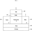
- FIG. 1 is a drawing for describing leakage current between adjacent cells in a conventional DRAM.
- a conventional capacitorless DRAM forms oxide 205 on a substrate 206, forms source 101, a floating body 104, a drain 103 on the oxide 205, and forms oxide and a gate 102 on the floating body 104.
- the source 101, the drain 103, and the gate 102 are electrically connected with the outside, the floating body 104 is electrically floated because the floating body 104 has the oxide on the top and bottom sides and the source and the drain on both sides.
- the source 101, the floating body 104, and the drain 103 may be n, p, n or p, n, n type of semiconductor, it will be described as an example of n, p, n type.
- the conventional capacitorless DRAM may use impact ionization effect as a writing method.
- impact ionization effect when a positive voltage is applied to the drain 103, and also a positive voltage is applied to the gate 102, electron is injected through the source 101, and the injected electron creates impact ionization effect by strong electric field near the drain 103. Electron and hole are generated by impact ionization effect.
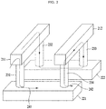
- FIG. 2 is a drawing for describing a structure of a conventional capacitorless DRAM.
- FIG. 2 shows a part of memory array, and illustrates four cells 231, 232, 233, 234, word lines 211, 212, bit lines 221, 222, data current 241, and leakage current 242.
- the data current 241 which is generated when a voltage is applied to the word line 211 has information for a first cell 231. If the spaces between the four cells 231, 232, 233, 234 are small and second, third, and fourth cells are under low resistance state, the leakage current through the second, third, and fourth cells 232, 233, 234 flows in the bit line 221. In this case, because the data current 241 indicating information for the first cell 231 and the leakage current 242 are combined and flow in the bit line 221, there is a problem that information for the first cell 231 may not be accurately known even though the combined current is measured.
- abiristoraccording to this invention may solve leakage current problem by adjacent cell so as not to flow reverse current through asymmetric doping.
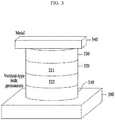
- FIG. 3 is a drawing for describing a structure of a vertical-type asymmetric two-terminal biristor according to an example of embodiments.
- a vertical-type asymmetric two-terminal biristor is a vertical-type structure including a substrate 300, a first semiconductor layer 310, a second semiconductor layer 320, a third semiconductor layer 330, and a metal electrode 340.
- an area of a unit cell is limited with 8F 2 or 6F 2 on characteristic of an existing horizontal-type DRAM, because the asymmetric two-terminal biristoraccording to this invention has vertical-type, an area of a unit cell may be 4F 2 .
- the substrate 300 may be material based on germanium having smaller band gap energy than silicon (band gap energy is about 1.12 eV), for example, germanium wafer, Si-Ge (silicon-germanium) alloy based wafer, GOI (germanium on insulator) wafer, SGOI (strained germanium on insulator) wafer.
- germanium wafer Si-Ge (silicon-germanium) alloy based wafer
- GOI germanium on insulator
- SGOI strained germanium on insulator
- the wafer may be produced by using at least one of Czochralski method, Floating zone method, Bridgman method, Casting method, EMC (Electro-magnetic casting) method.
- the band gap energy is the minimum energy for electron existing in valence band to be excited in conduction band.
- the electron of valence band fixed by nucleus gets band gap energy and is excited to conduction band, the electron becomes free electron because it may freely move, and it affects current flow.
- the biristor is created based on germanium which has smaller band gap energy than silicon, it is advantageous to make a low power device because high voltage current may flow in the biristor even though a low voltage is applied.
- the semiconductor layers 310, 320, 330 may be formed through epitaxial growth, selective epitaxial growth, or ion implantation.
- the epitaxial growth is a process for growing a layer having the same crystal structure with a semiconductor substrate, and for example, it may be PVD (Physical Vapor Deposition), CVD (Chemical Vapor Deposition), MOCVD (Metal-Organic Chemical Vapor Deposition), and ALD (Atomic Layer Deposition).
- PVD Physical Vapor Deposition
- CVD Chemical Vapor Deposition
- MOCVD Metal-Organic Chemical Vapor Deposition
- ALD Atomic Layer Deposition
- the selective epitaxial growth is a process for exposing a certain area of a semiconductor substrate, and growing a layer having the same crystal structure with the exposed area.
- the selective epitaxial growth is easy to produce a semiconductor device having a three-dimensional structure.
- the first semiconductor layer 310 and the third semiconductor layer 330 are different types of semiconductor from the second semiconductor layer 320.
- the second semiconductor 320 may be N type semiconductor
- the first semiconductor layer 310 and the third semiconductor layer 330 are N type semiconductors
- the second semiconductor layer 320 may be P type semiconductor.
- an external voltage may be applied to each of the first semiconductor layer 310 and the third semiconductor layer 330, and the second semiconductor layer 320 is in floating state thatan external voltage may not be directly applied.
- the second semiconductor layer 320 may include a first area 321 and a second area 322 having different doping concentration. A leakage current problem through adjacent cell may be blocked by including the first area 321 and the second area 322 having different doping concentration in the second semiconductor layer 320.
- the first semiconductor layer 310 and the third semiconductor layer 330 are formed in N type
- the second semiconductor layer 320 is formed in P type
- each of the first and second areas 321, 322 is formed in P + and P 0
- a current indicating '0' and '1' may flow.
- the second semiconductor layer 320 may form an energy well where electric charge may be accumulated since the band gap energy changes band gap by repeatedly forming different substances or adjusting the rate of Ge in SiGe compound structure.
- the second semiconductor layer 320 may be formed by at least one substance of III-IV compound and Si and Ge.
- Example of a structure forming the energy well may include GaN/InGaN laminated structure, InAs/In 1-x Ga x As (e.g., InAs/In 0.8 Ga 0.2 As), AlxGai-xAs/GaAs (e.g., Al 0.2 Ga 0.8 As/GaAs), and Si/Sii-xGex (e.g., Si/Si 0.8 Ge 0.2 ), and here, x may mean a value for adjusting content concentration.
- InAs/In 1-x Ga x As e.g., InAs/In 0.8 Ga 0.2 As
- AlxGai-xAs/GaAs e.g., Al 0.2 Ga 0.8 As/GaAs
- Si/Sii-xGex e.g., Si/Si 0.8 Ge 0.2
- x may mean a value for adjusting content concentration.
- An example of embodiments is a two-terminal structure removing gate and insulator layer in the existing device of three-terminal structure of gate, source, and drain.
- an electron-hole pair may be formed by impact ionization. If excess hole or electron is accumulated in the second semiconductor layer, it is in low resistance state, so '1' state may be indicated by flowing high current.
- a voltage of specific bias may be applied to between the first and third semiconductor layers. Because it is in high resistance state by disappearing excess hole or electron in the second semiconductor layer by the specific bias voltage, '0' state may be indicated by flowing low current. Since the two resistance states may be maintained according to bias, the device according to this invention may be defined as Biristor (bistable resistor), and here, DRAM which may determine whether data is stored or not based on current difference of the two states may be implemented.
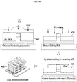
- FIG. 4A and FIG. 4B are drawings for describing a method for manufacturing a vertical-type asymmetric two-terminal biristor according to an example of embodiments.
- An example of embodiments may include forming a substrate which is a wafer based on P type germanium S 410.
- the substrate 300 may be a substance having smaller band gap than silicon (band gap is about 1.12 eV), for example, germanium wafer, GOI (Germanium on Insulator) wafer, SGOI (Strained Germanium on Insulator) wafer.
- the wafer may be produced by using at least one of Czochralski method, Floating zone method, Bridgeman method, Casting method, and EMC (Electro-Magnetic Casting) method.
- a semiconductor layer on the germanium based substrate may be included S420.
- a method for forming the semiconductor layer at least one of epitaxial growth, selective epitaxial growth, ion implantation may be used.
- different types of semiconductor layer may be formed by adjusting acceleration energy of ion implantation and dose amount of impurities.
- implanted ion may be activated, and distribution of the implanted ion may be adjusted as desired form. Annealing is a method for heating a semiconductor at a high temperature for a specific time period, and then, cooling relatively slowly.
- doping concentration of the bottom may be lower than doping concentration of the top.
- Current may flows as desired direction by making different doping concentration. In other words, it may be prevented from occurring undesired current by being affected by adjacent cell.
- the hard mask may include depositing a hard mask in order to form an active semiconductor layer S430.
- the hard mask performs a role to prevent desired circuit pattern from being etched.
- the hard mask may be a substance such as armorphous carbon, Si 3 N 4 , and SiO 2 .
- ACL Armorphous Carbon Layer
- an example of embodiments may include patterning and dry etching S440.
- PR Photoresist
- the active semiconductor layer may be formed through patterning with Electron Beam Lithography and dry etching.
- the bottom of the first semiconductor layer may be used as common electrode, the bottom of the first semiconductor layer may be saved when etching.
- the process for patterning may be a method for recording circuit pattern of nano scale such as X-ray lithography as well as Electron Beam Lithography.
- this invention may improve characteristics of the biristor by removing defect of Ge pillar surface which is the vertically formed first to third semiconductor layers by additionally performing sacrificial oxidation after dry etching.
- this invention may remove defect state of Ge pillar surface by performing sacrificial oxidation, and improve characteristics of the biristor including reducing operation voltage, increasing electric charge storage retention time and reliability of cyclic endurance, and the like.
- S440 it may include depositing insulating substance after removing PR and SiNS450.
- An example of embodiments may block unnecessary electric interaction between activated semiconductor layers by depositing PE-TEOS. Therefore, substance which may perform a role of ILD as well as PE-TEOS may be deposited.
- planarization After S450, it may include planarization in order to make precise semiconductor device S460.
- a method for planarization may be used such as Chemical Mechanical Planarization and the like.
- Blanket Etch may be performed with BOE (Buffered Oxide Etch) solution thatNH 4 F solution and HF solution are mixed at 6:1 ratio as a buffer solution. Blanket Etch is an etching technology for thinly etching surface.
- the hard mask deposited on the third semiconductor layer, for example, ACL exists between the buffer solution and the third semiconductor layer. Therefore, it may prevent the third semiconductor layer from etching by being affected by the buffer solution.
- S470 it may include removing the remaining hard mask and forming metal electrode S480.
- An example of embodiments may use a semiconductor etching method such as etching through plasma oxidation as a method for removing the remaining hard mask.
- An array of a vertical-type two-terminal biristor based on germanium may be formed through a method by S410 to S480, S490. As shown in S490, to give various bias conditions through external voltage, cells which are arrayed in the same column may be connected with the bottom part of the first semiconductor layer, and cells which are arrayed in the same row may be connected with metal electrode.
- S490 to give various bias conditions through external voltage, cells which are arrayed in the same column may be connected with the bottom part of the first semiconductor layer, and cells which are arrayed in the same row may be connected with metal electrode.
- a conventional three-terminal semiconductor because it does not have a gate, it may perform a role of DRAM with two-terminal, and it may perform a role of a capacitor because it may maintain quantity of electric charge by excess carrier collected in the second semiconductor layer. Also, because leakage current by adjacent cell is small due to asymmetric doping area of the second semiconductor layer, current containing information of the desired cell may be obtained with high accuracy.
- FIG. 5A and FIG. 5B are current-voltage curve of a vertical-type asymmetric two-terminal biristor according to an example of embodiments.
- first, second, and third semiconductors are each of N, P, and N types
- EHPs Electro Hole pairs
- BJT Bipolar Junction Transistor
- latch down voltage V LD is smaller than the voltage which occurs in the breakdown region (hereafter, latch up voltage V LU , so there is bistable current-voltage characteristic between V LD and V LU . States that excess holes are collected or not collected in the second semiconductor layer may be sensed between V LD and V LU . According to the collected state of the excess carrier, current flows much or less. Therefore, it may distinguish whether the stored data is "1" state or "0" state.
- M is multiplication factor, and represents the ratio between current before impact and current by impact.
- ⁇ is current gain, and represents the ratio between base current and collector current in BJT.
- the multiplication factor M increases proportionally with a voltage applied to the third semiconductor layer. The current gain is described in detail in KR 10-1042521 .
- the hole by impact ionization is collected in the second semiconductor layer, and in low resistance state, so it may maintain high current although the voltage is lowered to some extent.
- FIG. 5B illustrates current-voltage curve in case that a negative voltage is applied to the third semiconductor layer, and the first semiconductor layer is grounded.
- the voltage of the same absolute value when applying a negative voltage than applying a positive voltage, multiplication factor and current gain are small. Therefore, because (M-1)* ⁇ ⁇ 1 may be satisfied only when applying bigger absolute value than applying the positive voltage, it is observed that no current flows in voltage section such as FIG. 5B .
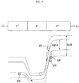
- FIG. 6 is a drawing for describing a band diagram of a vertical-type asymmetric two-terminal biristor according to an exampleof embodiments.
- band gap energy of two-terminal birister based on Ge is smaller than band gap energy of two-terminal biristor based on Si.
- the two-terminal biristor based on Ge having small band gap energy is compared with the biristor based on Si, it has an advantage that large current may flow by a small voltage. Therefore, the vertical-type asymmetric two-biristor according to this invention may be usefully used in manufacturing low power device.
- first and third semiconductor layers may be formed in P type, and a second semiconductor layer may be formed in N type.
- voltage level applied to the third semiconductor layer increases on a state that the first semiconductor layer is short-circuited, a hole 610 is injected, and the hole 610 is over contact potential between the first semiconductor layer and the second semiconductor layer. Then, impact ionization occurs by a high voltage between the second semiconductor layer and the third semiconductor layer, and electron-hole pair 620, 630 is generated.
- An excess hole 620 goes to the third semiconductor layer and becomes a part of drain current, and the excess electron 630 may not go to the first semiconductor layer by contact potential between the first semiconductor layer and the second semiconductor layer, and makes energy band high by being collected in the second semiconductor layer.
- contact potential of the hole viewing the second semiconductor layer from the first semiconductor layer is lower, so more holes are injected.
- the vertical-type asymmetric two-terminal biristor according to this invention is a device having positive feedback.
- Energy band gap of the first and second semiconductor layers and the second semiconductor layer may be different depending on material of each of layers.
- energy band gap of the first and third semiconductor layers is bigger than energy band gap of the second semiconductor layer. If energy band gap of the second semiconductor layer is made smaller than energy band gap of the first semiconductor layer and the third semiconductor layer, contact potential for the hole between the first semiconductor layer and the second semiconductor layer is lower, so the hole may easily go to the third semiconductor layer. On the contrary, because contact potential for the electron between the first semiconductor layer and second semiconductor layer is higher, there is high possibility that the electron moving down from the third semiconductor layer to the second semiconductor layer by impact ionization is blocked by contact potential, so it may not move to the first semiconductor layer, and be accumulated.
- FIG. 7 is a drawing for describing a positive feedback system of a vertical-type asymmetric two-terminal biristor according to an example of embodiments.
- Electron-hole pair generated by impact ionization generates another electron-hole pair by impact ionization again, and electrons accumulated in the second semiconductor layer makes contact potential lower, so larger current may flow.
- drain current Ic is a value that current I B flowing in the second semiconductor layer is multiplied by multiplication M and current gain ⁇ . Because the vertical-type asymmetrictwo-terminal biristor according to this invention has a positive feedback, a value obtained by multiplying drain current of the opened system and (M-1)/M is input again.
Landscapes
- Semiconductor Memories (AREA)
Abstract
Description
- This application claims the priority benefit of Korean Patent Application No.
10-2017-0089041, filed on July13, 2017 10-2018-0001459, filed on January 05, 2018 - The following example embodiments relate to a technology for a semiconductor memory device, further particularly, a vertical-type two-terminal gateless and capacitorless DRAM cell and a method for manufacturing thereof.
- A unit cell of a conventional DRAM memory is a structure (1T/1C) including one transistor (T) and one capacitor (C). In case of a memory device, as the number of cells per unit area increases, it brings commercially and economically excellent effects. Therefore, miniaturizing cell is the biggest problem to solve in a memory industry. To miniaturize cell, miniaturizing the size of transistor or capacitor is a core technology in a conventional DRAM cell structure. As technology is developed, it is possible to miniaturize the size of transistor, but miniaturizing the size of capacitor while maintaining the size of capacitance faces to technical limitation. To solve this problem, a capacitorless DRAM is suggested. Because a unit cell is configured with only one transistor without a capacitor in the capacitorless DRAM, it is advantageous to miniaturize cell. In other words, as it is miniaturized, it may have high density, and manufacturing process is simple, which is advantageous for commercialization. However, in case of the capacitorless DRAM, sincea high driving voltage is required in a process of reading and writing memory status, gate insulation degradation occurs, and because of this, there is a critical problem for reliability and durability among memory operation characteristics.
- At least one example of embodiments may provide a vertical-type asymmetric two-terminal biristor and a method for manufacturing a two-terminal biristor, which may fundamentally solve a problem due to gate insulation degradation occurred in a capacitorelss DRAM having above three-terminal and reduce production cost by omitting processing step for forming gate and gate insulation.
- At least one example of embodiments may provide a vertical-type asymmetric two-terminal biristor and a method for manufacturing a two-terminal biristor, which may reduce power consumption by operating in lower voltage by manufacturing based on germanium having small band gap instead of silicon.
- At least one example of embodiments may provide a vertical-type asymmetric two-terminal bristor and a method for manufacturing a two-terminal biristor, which may protect germanium which is affected by wet etchant by depositing ACL (Amorphous Carbon Layer) on processing wet etching of ILD (Inter-Layer Dielectric).
- At least one example of embodiments may provide a vertical-type asymmetric two-terminal biristor and a method for manufacturing a two-terminal biristor, which may solve reverse leakage current through adjacent cell by using semiconductor layer having asymmetric doping area.
- According to at least one example embodiment, a method for manufacturing a vertical-type asymmetrictwo-terminal biristormay include forming a first semiconductor layer on a substrate including germanium, forming a second semiconductor layer based on germanium including a first area and a second area which have different doping concentration on the first semiconductor layer, and forming a third semiconductor layer based on germanium on the second semiconductor layer, and the first and third semiconductor layers and the second semiconductor layer may be different types of semiconductor layers.
- The substrate including germanium may include one of pure Ge (germanium), GeOI (Ge on Insulator), or SGOI (Strained Germanium on Insulator).
- When the first and third semiconductor layers are formed in N type, and the second semiconductor layer is formed in P type, balance band energy of the first and third semiconductor layers may be lower than balance band energy of the second semiconductor layer, and conduction band energy of the second semiconductor layer may be higher than conduction band energy of the first and third semiconductor layers.
- When the first and third semiconductor layers are formed in P type, and the second semiconductor layer is formed in N type, balance band energy of the first and third semiconductor layers may be higher than balance band energy of the second semiconductor layer, and conduction band energy of the second semiconductor layer may be lower than conduction band energy of the first and third semiconductor layers.
- The forming second semiconductor layer may include forming the first area to N+ and the second area to N0 or forming the first area to N0 and the second area to N+ when the first and third semiconductor layers are formed in P type.
- The forming second semiconductor layer may include forming the first area to P+ and the second area to P0 or forming the first area to P0 and the second area to P+ when the first and third semiconductor layers are formed in N type.
- The forming first and third semiconductor layers may include forming through ion implantation.
- Furthermore, annealing for the first and third semiconductor layers may be further included.
- The forming first and third semiconductor layers may include forming through epitaxial growth or selective epitaxial growth.
- The forming first and third semiconductor layers may include forming energy band gap of the first and third semiconductor layers to be bigger than energy band gap of the second semiconductor layer.
- The method may further include patterning and etching the semiconductor layers with activation semiconductor layer, and depositing ILD (Inter-Layer Dielectric) and metal line.
- The method may further include depositing ACL (Amorphous Carbon Layer) on the third semiconductor layer in order to protect the third semiconductor layer when etching the ILD.
- The method may further include forming sacrificial oxide layer on pillar surface including the first to third semiconductor layers which are vertically formed by the etching.
- The forming second semiconductor layer may form the second semiconductor layer by laminating a plurality of substances having different band gap energy or form the second semiconductor layer by adjusting rate of germanium to a certain rate in order to forman energy well.
- According to another aspect of at least one example embodiment, a vertical-type asymmetrictwo-terminal biristormay be manufactured by any one of the above methods.
- According to another aspect of at least one example embodiment, a vertical-type asymmetric two-terminal biristormay include a substrate based on germanium, a first semiconductor layer of a first type formed on the substrate, a second semiconductor layer of a second type formed on the first semiconductor layer and including a first area and a second area which have different doping concentration, and a third semiconductor layer of the first type formed on the second semiconductor layer.
- The substrate based on germanium may be based on one of pure Ge, GeOI, or SGOI.
- When the first type is P type, and the second type is N type, the first area may be doped with N+ and the second area may be doped with N0, or the first area may be dope with N0 and the second area may be doped with N+.
- When the first type is N type, and the second type is P type, the first area may be doped with P+ and the second area may be doped with P0, or the first area may be dope with P0 and the second area may be doped with P+.
- When the first type is P type, and the second type is N type, balance band energy of the first and third semiconductor layers may be higher than balance band energy of the second semiconductor layer, and conduction band energy of the second semiconductor layer may be lower than conduction band energy of the first and third semiconductor layers.
- When the first type is N type, and the second type is P type, balance band energy of the first and third semiconductor layers may be lower than balance band energy of the second semiconductor layer, and conduction band energy of the second semiconductor layer may be higher than conduction band energy of the first and third semiconductor layers.
- The second semiconductor layer may have smaller energy band gap than the first and third semiconductor layers.
- According to example embodiments, it may fundamentally solve a problem due to gate insulation degradation occurred in a capacitorless DRAM having above three-terminal and reduce production cost by omitting processing step for forming gate and gate insulation.
- According to example embodiments, it may remove affectionof wet etchant on a third semiconductor layer by depositing ACL (Amorphous Carbon Layer) on the third semiconductor layer in advance on processing wet etching of ILD (Inter-Layer Dielectric).
- According to example embodiments, it may reduce power consumption by operating in lower voltage by manufacturing based on germanium having small band gap instead of silicon.
- According to example embodiments, it may solve reverse leakage current through adjacent cell by using semiconductor layer having asymmetric doping area.
- These and/or other aspects, features, and advantages of the invention will become apparent and more readily appreciated from the following description of embodiments, taken in conjunction with the accompanying drawings of which:
-
FIG. 1 is a drawing for describing leakage current between adjacent cells in a conventional DRAM; -
FIG. 2 is a drawing for describing a structure of a conventional capacitorless DRAM; -
FIG. 3 is a drawing for describing a structure of a vertical-type asymmetric two-terminal biristor according to an example of embodiments; -
FIG. 4A andFIG. 4B are drawings for describing a method for manufacturing a vertical-type asymmetric two-terminal biristor according to an example of embodiments; -
FIG. 5A andFIG. 5B are current-voltage curve of a vertical-type asymmetrictwo-terminal biristor according to an example of embodiments; -
FIG. 6 is a drawing for describing a band diagram of a vertical-type asymmetric two-terminal biristor according to an example of embodiments; and -
FIG. 7 is a drawing for describing a positive feedback system of a vertical-type asymmetric two-terminal biristor according to an example of embodiments. - Hereinafter, some example embodiments will be described in detail with reference to the accompanying drawings.
-
FIG. 1 is a drawing for describing leakage current between adjacent cells in a conventional DRAM. - Referring to
FIG. 1 , a conventional capacitorless DRAM forms oxide 205 on a substrate 206, formssource 101, afloating body 104, adrain 103 on the oxide 205, and forms oxide and agate 102 on thefloating body 104. Although thesource 101, thedrain 103, and thegate 102 are electrically connected with the outside, thefloating body 104 is electrically floated because thefloating body 104 has the oxide on the top and bottom sides and the source and the drain on both sides. Although thesource 101, thefloating body 104, and thedrain 103 may be n, p, n or p, n, n type of semiconductor, it will be described as an example of n, p, n type. - The conventional capacitorless DRAM may use impact ionization effect as a writing method. In other words, when a positive voltage is applied to the
drain 103, and also a positive voltage is applied to thegate 102, electron is injected through thesource 101, and the injected electron creates impact ionization effect by strong electric field near thedrain 103. Electron and hole are generated by impact ionization effect. - Because electron and hole generated between the floating
body 104 and thedrain 103 try to go to low energy state, the electron goes out to thedrain 103, and the hole goes to the floatingbody 104. Here, when energy gap of the floatingbody 104 is designed to be smaller than thesource 101 and thedrain 103, contact potential for electron among contact potential between the floatingbody 104 and thedrain 103 is bigger than contact potential for hole. Therefore, hole came from thedrain 103 to the floatingbody 104 is accumulated, and there are very few holesgoing to the source. - More detailed contents for the conventional capacitorless DRAM may be described through Korean Patent No.
10-1042521 -
FIG. 2 is a drawing for describing a structure of a conventional capacitorless DRAM. -
FIG. 2 shows a part of memory array, and illustrates fourcells bit lines - The data current 241 which is generated when a voltage is applied to the
word line 211 has information for afirst cell 231. If the spaces between the fourcells fourth cells bit line 221. In this case, because the data current 241 indicating information for thefirst cell 231 and the leakage current 242 are combined and flow in thebit line 221, there is a problem that information for thefirst cell 231 may not be accurately known even though the combined current is measured. - Although leakage current was prevented by making an array with adding a diode in the past, abiristoraccording to this invention may solve leakage current problem by adjacent cell so as not to flow reverse current through asymmetric doping.
-
FIG. 3 is a drawing for describing a structure of a vertical-type asymmetric two-terminal biristor according to an example of embodiments. - Referring to
FIG. 3 , a vertical-type asymmetric two-terminal biristor is a vertical-type structure including asubstrate 300, afirst semiconductor layer 310, asecond semiconductor layer 320, athird semiconductor layer 330, and ametal electrode 340. - Although an area of a unit cell is limited with 8F2 or 6F2 on characteristic of an existing horizontal-type DRAM, because the asymmetric two-terminal biristoraccording to this invention has vertical-type, an area of a unit cell may be 4F2.
- The
substrate 300 may be material based on germanium having smaller band gap energy than silicon (band gap energy is about 1.12 eV), for example, germanium wafer, Si-Ge (silicon-germanium) alloy based wafer, GOI (germanium on insulator) wafer, SGOI (strained germanium on insulator) wafer. - The wafer may be produced by using at least one of Czochralski method, Floating zone method, Bridgman method, Casting method, EMC (Electro-magnetic casting) method.
- The band gap energy is the minimum energy for electron existing in valence band to be excited in conduction band. When the electron of valence band fixed by nucleus gets band gap energy and is excited to conduction band, the electron becomes free electron because it may freely move, and it affects current flow. In other words, if the biristor is created based on germanium which has smaller band gap energy than silicon, it is advantageous to make a low power device because high voltage current may flow in the biristor even though a low voltage is applied.
- The semiconductor layers 310, 320, 330 may be formed through epitaxial growth, selective epitaxial growth, or ion implantation.
- The epitaxial growth is a process for growing a layer having the same crystal structure with a semiconductor substrate, and for example, it may be PVD (Physical Vapor Deposition), CVD (Chemical Vapor Deposition), MOCVD (Metal-Organic Chemical Vapor Deposition), and ALD (Atomic Layer Deposition).
- The selective epitaxial growth is a process for exposing a certain area of a semiconductor substrate, and growing a layer having the same crystal structure with the exposed area. The selective epitaxial growth is easy to produce a semiconductor device having a three-dimensional structure.
- The
first semiconductor layer 310 and thethird semiconductor layer 330 are different types of semiconductor from thesecond semiconductor layer 320. For example, if thefirst semiconductor layer 310 and thethird semiconductor layer 330 are P type semiconductors, thesecond semiconductor 320 may be N type semiconductor, and if thefirst semiconductor layer 310 and thethird semiconductor layer 330 are N type semiconductors, thesecond semiconductor layer 320 may be P type semiconductor. - To flow current in the semiconductor, an external voltage may be applied to each of the
first semiconductor layer 310 and thethird semiconductor layer 330, and thesecond semiconductor layer 320 is in floating state thatan external voltage may not be directly applied. - The
second semiconductor layer 320 may include afirst area 321 and asecond area 322 having different doping concentration. A leakage current problem through adjacent cell may be blocked by including thefirst area 321 and thesecond area 322 having different doping concentration in thesecond semiconductor layer 320. For example, when thefirst semiconductor layer 310 and thethird semiconductor layer 330 are formed in N type, thesecond semiconductor layer 320 is formed in P type, and each of the first andsecond areas - Furthermore, the
second semiconductor layer 320 may form an energy well where electric charge may be accumulated since the band gap energy changes band gap by repeatedly forming different substances or adjusting the rate of Ge in SiGe compound structure. - Here, the
second semiconductor layer 320 may be formed by at least one substance of III-IV compound and Si and Ge. - Example of a structure forming the energy well may include GaN/InGaN laminated structure, InAs/In1-xGaxAs (e.g., InAs/In0.8Ga0.2As), AlxGai-xAs/GaAs (e.g., Al0.2Ga0.8As/GaAs), and Si/Sii-xGex (e.g., Si/Si0.8Ge0.2), and here, x may mean a value for adjusting content concentration.
- An example of embodiments is a two-terminal structure removing gate and insulator layer in the existing device of three-terminal structure of gate, source, and drain. To indicate '1' state, an electron-hole pair may be formed by impact ionization. If excess hole or electron is accumulated in the second semiconductor layer, it is in low resistance state, so '1' state may be indicated by flowing high current. To indicate '0' state, a voltage of specific bias may be applied to between the first and third semiconductor layers. Because it is in high resistance state by disappearing excess hole or electron in the second semiconductor layer by the specific bias voltage, '0' state may be indicated by flowing low current. Since the two resistance states may be maintained according to bias, the device according to this invention may be defined as Biristor (bistable resistor), and here, DRAM which may determine whether data is stored or not based on current difference of the two states may be implemented.
-
FIG. 4A andFIG. 4B are drawings for describing a method for manufacturing a vertical-type asymmetric two-terminal biristor according to an example of embodiments. - An example of embodiments may include forming a substrate which is a wafer based on P
type germanium S 410. Thesubstrate 300 may be a substance having smaller band gap than silicon (band gap is about 1.12 eV), for example, germanium wafer, GOI (Germanium on Insulator) wafer, SGOI (Strained Germanium on Insulator) wafer. - The wafer may be produced by using at least one of Czochralski method, Floating zone method, Bridgeman method, Casting method, and EMC (Electro-Magnetic Casting) method.
- After S410, forming a semiconductor layer on the germanium based substrate may be included S420. As a method for forming the semiconductor layer, at least one of epitaxial growth, selective epitaxial growth, ion implantation may be used. Here, when forming the semiconductor layer with ion implantation, different types of semiconductor layer may be formed by adjusting acceleration energy of ion implantation and dose amount of impurities. Also, by including annealing, implanted ion may be activated, and distribution of the implanted ion may be adjusted as desired form. Annealing is a method for heating a semiconductor at a high temperature for a specific time period, and then, cooling relatively slowly.
- When forming the second semiconductor layer, doping concentration of the bottom may be lower than doping concentration of the top. Current may flows as desired direction by making different doping concentration. In other words, it may be prevented from occurring undesired current by being affected by adjacent cell.
- After S420, it may include depositing a hard mask in order to form an active semiconductor layer S430. The hard mask performs a role to prevent desired circuit pattern from being etched. In an example of embodiments, the hard mask may be a substance such as armorphous carbon, Si3N4, and SiO2. For example, by depositing ACL (Armorphous Carbon Layer) on the third semiconductor layer, afterward in an etching process, it may be prevented the third semiconductor layer from being etched at least partly.
- After S430, an example of embodiments may include patterning and dry etching S440. After depositing PR (Photoresist) on the hard mask, the active semiconductor layer may be formed through patterning with Electron Beam Lithography and dry etching. Here, when arraying cell, since the bottom of the first semiconductor layer may be used as common electrode, the bottom of the first semiconductor layer may be saved when etching. The process for patterning may be a method for recording circuit pattern of nano scale such as X-ray lithography as well as Electron Beam Lithography.
- Furthermore, this invention may improve characteristics of the biristor by removing defect of Ge pillar surface which is the vertically formed first to third semiconductor layers by additionally performing sacrificial oxidation after dry etching. In case of the two-terminal biristor, it is very important characteristic that electric charges additionally generated by impact ionization are maintained on the second semiconductor layer which is a base area without being recombined. However, in the case of dry etching which proceeds to form Ge pillar, it may physically damage around Ge pillar. Therefore, this invention may remove defect state of Ge pillar surface by performing sacrificial oxidation, and improve characteristics of the biristor including reducing operation voltage, increasing electric charge storage retention time and reliability of cyclic endurance, and the like.
- After S440, it may include depositing insulating substance after removing PR and SiNS450. An example of embodiments may block unnecessary electric interaction between activated semiconductor layers by depositing PE-TEOS. Therefore, substance which may perform a role of ILD as well as PE-TEOS may be deposited.
- After S450, it may include planarization in order to make precise semiconductor device S460. A method for planarization may be used such as Chemical Mechanical Planarization and the like.
- After S460, it may include etching in order to remove remaining hard mask part which is ACL (Amorphous Carbon Layer) in an example of embodimentsS470. Since electrical interaction between semiconductor layers is blocked by the insulating substance, large amounts of substrates may be processed through wet etching rather than precisely etching. For example, Blanket Etch may be performed with BOE (Buffered Oxide Etch) solution thatNH4F solution and HF solution are mixed at 6:1 ratio as a buffer solution. Blanket Etch is an etching technology for thinly etching surface. The hard mask deposited on the third semiconductor layer, for example, ACL exists between the buffer solution and the third semiconductor layer. Therefore, it may prevent the third semiconductor layer from etching by being affected by the buffer solution.
- After S470, it may include removing the remaining hard mask and forming metal electrode S480. An example of embodiments may use a semiconductor etching method such as etching through plasma oxidation as a method for removing the remaining hard mask.
- An array of a vertical-type two-terminal biristor based on germanium may be formed through a method by S410 to S480, S490. As shown in S490, to give various bias conditions through external voltage, cells which are arrayed in the same column may be connected with the bottom part of the first semiconductor layer, and cells which are arrayed in the same row may be connected with metal electrode. When comparing with a conventional three-terminal semiconductor, because it does not have a gate, it may perform a role of DRAM with two-terminal, and it may perform a role of a capacitor because it may maintain quantity of electric charge by excess carrier collected in the second semiconductor layer. Also, because leakage current by adjacent cell is small due to asymmetric doping area of the second semiconductor layer, current containing information of the desired cell may be obtained with high accuracy.
-
FIG. 5A andFIG. 5B are current-voltage curve of a vertical-type asymmetric two-terminal biristor according to an example of embodiments. - In case that first, second, and third semiconductors are each of N, P, and N types, when a voltage of the third semiconductor layer increases, impact ionization occurs by high electric field formed between the second and third semiconductor layers, and EHPs (Electron Hole pairs) are generated. Excess electrons pass through the second semiconductor layer to the third semiconductor layer, and when a voltage reaches to a specific value, large current flows such as BJT (Bipolar Junction Transistor) whose base is opened is in breakdown region. Here, current of large value is maintained as long as the voltage of above specific value is applied. If the voltage reduces again, generation of EHPs reduces, and it is again out of the breakdown region, so small current flows. The voltage which is out of the breakdown region (hereafter, latch down voltage VLD is smaller than the voltage which occurs in the breakdown region (hereafter, latch up voltage VLU, so there is bistable current-voltage characteristic between VLD and VLU. States that excess holes are collected or not collected in the second semiconductor layer may be sensed between VLD and VLU. According to the collected state of the excess carrier, current flows much or less. Therefore, it may distinguish whether the stored data is "1" state or "0" state.
- In other words, when a positive voltage is applied to the third semiconductor layer, and the first semiconductor layer is grounded, as illustrated in
FIG. 5A , drain current rarely flows until VLU is reached, and the drain current rapidly rises by impact ionization when VLU is reached. Here, a rapid increase of current occurs when satisfying (M-1)*β ≒ 1. M is multiplication factor, and represents the ratio between current before impact and current by impact. β is current gain, and represents the ratio between base current and collector current in BJT. The multiplication factor M increases proportionally with a voltage applied to the third semiconductor layer. The current gain is described in detail inKR 10-1042521 - The hole by impact ionization is collected in the second semiconductor layer, and in low resistance state, so it may maintain high current although the voltage is lowered to some extent.
-
FIG. 5B illustrates current-voltage curve in case that a negative voltage is applied to the third semiconductor layer, and the first semiconductor layer is grounded. In case of the voltage of the same absolute value, when applying a negative voltage than applying a positive voltage, multiplication factor and current gain are small. Therefore, because (M-1)*β ≒ 1 may be satisfied only when applying bigger absolute value than applying the positive voltage, it is observed that no current flows in voltage section such asFIG. 5B . -
FIG. 6 is a drawing for describing a band diagram of a vertical-type asymmetric two-terminal biristor according to an exampleof embodiments. - Referring to
FIG. 6 , band gap energy of two-terminal birister based on Ge is smaller than band gap energy of two-terminal biristor based on Si. When the two-terminal biristor based on Ge having small band gap energy is compared with the biristor based on Si, it has an advantage that large current may flow by a small voltage. Therefore, the vertical-type asymmetric two-biristor according to this invention may be usefully used in manufacturing low power device. - Also, referring to
FIG. 6 , in an example of embodiments, first and third semiconductor layers may be formed in P type, and a second semiconductor layer may be formed in N type. When voltage level applied to the third semiconductor layer increases on a state that the first semiconductor layer is short-circuited, ahole 610 is injected, and thehole 610 is over contact potential between the first semiconductor layer and the second semiconductor layer. Then, impact ionization occurs by a high voltage between the second semiconductor layer and the third semiconductor layer, and electron-hole pair excess hole 620 goes to the third semiconductor layer and becomes a part of drain current, and theexcess electron 630 may not go to the first semiconductor layer by contact potential between the first semiconductor layer and the second semiconductor layer, and makes energy band high by being collected in the second semiconductor layer. As electrons are accumulated in the second semiconductor layer, contact potential of the hole viewing the second semiconductor layer from the first semiconductor layer is lower, so more holes are injected. As more holes are injected, there are more electron-hole pairs generated by impact ionization, so drain current is larger. Therefore, the vertical-type asymmetric two-terminal biristor according to this invention is a device having positive feedback. - Energy band gap of the first and second semiconductor layers and the second semiconductor layer may be different depending on material of each of layers.
- Referring to
FIG. 6 , when comparing energy band gap of the first and third semiconductor layers and the second semiconductor layer, it may be shown that energy band gap of the first and third semiconductor layers is bigger than energy band gap of the second semiconductor layer. If energy band gap of the second semiconductor layer is made smaller than energy band gap of the first semiconductor layer and the third semiconductor layer, contact potential for the hole between the first semiconductor layer and the second semiconductor layer is lower, so the hole may easily go to the third semiconductor layer. On the contrary, because contact potential for the electron between the first semiconductor layer and second semiconductor layer is higher, there is high possibility that the electron moving down from the third semiconductor layer to the second semiconductor layer by impact ionization is blocked by contact potential, so it may not move to the first semiconductor layer, and be accumulated. -
FIG. 7 is a drawing for describing a positive feedback system of a vertical-type asymmetric two-terminal biristor according to an example of embodiments. - Electron-hole pair generated by impact ionization generates another electron-hole pair by impact ionization again, and electrons accumulated in the second semiconductor layer makes contact potential lower, so larger current may flow.
- When there is no feedback system, drain current Ic is a value that current IB flowing in the second semiconductor layer is multiplied by multiplication M and current gain β. Because the vertical-type asymmetrictwo-terminal biristor according to this invention has a positive feedback, a value obtained by multiplying drain current of the opened system and (M-1)/M is input again.
- While certain example embodiments and implementations have been described herein, other embodiments and modifications will be apparent from this description. Accordingly, the invention is not limited to such embodiments, but rather to the broader scope of the presented claims and various obvious modifications and equivalent arrangements.
Claims (15)
- A method for manufacturing a vertical-type asymmetrictwo-terminal biristor comprising:forming a first semiconductor layer on a substrate including germanium;forming a second semiconductor layer based on germanium including a first area and a second area which have different doping concentration on the first semiconductor layer; andforming a third semiconductor layer based on germanium on the second semiconductor layer,and the first and third semiconductor layers and the second semiconductor layer are different types of semiconductor layers.
- The method of claim 1, wherein the substrate including germanium comprises one of pure Ge (germanium), GeOI (Ge on Insulator), or SGOI (Strained Germanium on Insulator).
- The method of claim 1, wherein when the first and third semiconductor layers are formed in N type, and the second semiconductor layer is formed in P type, balance band energy of the first and third semiconductor layers are lower than balance band energy of the second semiconductor layer, and conduction band energy of the second semiconductor layer is higher than conduction band energy of the first and third semiconductor layers.
- The method of claim 1, wherein when the first and third semiconductor layers are formed in P type, and the second semiconductor layer is formed in N type, balance band energy of the first and third semiconductor layers are higher than balance band energy of the second semiconductor layer, and conduction band energy of the second semiconductor layer is lower than conduction band energy of the first and third semiconductor layers.
- The method of claim 1, wherein the forming second semiconductor layer comprises forming the first area to N+ and the second area to N0 or forming the first area to N0 and the second area to N+ when the first and third semiconductor layers are formed in P type.
- The method of claim 1, wherein the forming second semiconductor layer comprises forming the first area to P+ and the second area to P0 or forming the first area to P°and the second area to P+ when the first and third semiconductor layers are formed in N type.
- The method of claim 1, wherein the forming first and third semiconductor layers comprises forming energy band gap of the first and third semiconductor layers to be bigger than energy band gap of the second semiconductor layer.
- The method of any one of claims 1 to 7 further comprising patterning and etching the semiconductor layers with activation semiconductor layer; and depositing ILD (Inter-Layer Dielectric) and metal line.
- The method of claim 8 further comprising forming sacrificial oxide layer on pillar surface including the first to third semiconductor layers which are vertically formed by the etching.
- The method of claim 1, wherein the forming second semiconductor layer forms the second semiconductor layer by laminating a plurality of substances having different band gap energy or forms the second semiconductor layer by adjusting rate of germanium to a certain rate in order to forman energy well.
- A vertical-type asymmetrictwo-terminal biristor comprising:a substrate based on germanium;a first semiconductor layer of a first type formed on the substrate;a second semiconductor layer of a second type formed on the first semiconductor layer and including a first area and a second area which have different doping concentration; anda third semiconductor layer of the first type formed on the second semiconductor layer.
- The vertical-type asymmetrictwo-terminal biristor of claim 11, wherein when the first type is P type, and the second type is N type, the first area is doped with N+ and the second area is doped with N0, or the first area is dope with N0 and the second area is doped with N+.
- The vertical-type asymmetrictwo-terminal biristor of claim 11, wherein when the first type is N type, and the second type is P type, the first area is doped with P+ and the second area is doped with P0, or the first area is dope with P0 and the second area is doped with P+.
- The vertical-type asymmetrictwo-terminal biristor of claim 11, wherein when the first type is P type, and the second type is N type, balance band energy of the first and third semiconductor layers is higher than balance band energy of the second semiconductor layer, and conduction band energy of the second semiconductor layer is lower than conduction band energy of the first and third semiconductor layers.
- The vertical-type asymmetrictwo-terminal biristor of claim 11, wherein when the first type is N type, and the second type is P type, balance band energy of the first and third semiconductor layers is lower than balance band energy of the second semiconductor layer, and conduction band energy of the second semiconductor layer is higher than conduction band energy of the first and third semiconductor layers.
Applications Claiming Priority (2)
| Application Number | Priority Date | Filing Date | Title |
|---|---|---|---|
| KR20170089041 | 2017-07-13 | ||
| KR1020180001459A KR102103630B1 (en) | 2017-07-13 | 2018-01-05 | The vertical-type gateless and capacitorless dram cell based on germanium and the method for manufacturing thereof |
Publications (2)
| Publication Number | Publication Date |
|---|---|
| EP3428972A1 true EP3428972A1 (en) | 2019-01-16 |
| EP3428972B1 EP3428972B1 (en) | 2020-03-11 |
Family
ID=62951875
Family Applications (1)
| Application Number | Title | Priority Date | Filing Date |
|---|---|---|---|
| EP18183260.1A Active EP3428972B1 (en) | 2017-07-13 | 2018-07-12 | Vertical asymmetric germanium-based two-terminal biristor for vertical-type gateless and capacitorless dram cell and method for manufacturing thereof |
Country Status (1)
| Country | Link |
|---|---|
| EP (1) | EP3428972B1 (en) |
Citations (2)
| Publication number | Priority date | Publication date | Assignee | Title |
|---|---|---|---|---|
| KR101042521B1 (en) | 2009-06-30 | 2011-06-20 | 한국과학기술원 | Capacitorless DRAM, How to Write and Read |
| WO2014092224A1 (en) * | 2012-12-15 | 2014-06-19 | 한국과학기술원 | Asymmetrical 2-terminal biristor element and method of manufacturing same |
-
2018
- 2018-07-12 EP EP18183260.1A patent/EP3428972B1/en active Active
Patent Citations (2)
| Publication number | Priority date | Publication date | Assignee | Title |
|---|---|---|---|---|
| KR101042521B1 (en) | 2009-06-30 | 2011-06-20 | 한국과학기술원 | Capacitorless DRAM, How to Write and Read |
| WO2014092224A1 (en) * | 2012-12-15 | 2014-06-19 | 한국과학기술원 | Asymmetrical 2-terminal biristor element and method of manufacturing same |
Non-Patent Citations (2)
| Title |
|---|
| DONG-IL MOON ET AL: "Highly endurable floating body cell memory: Vertical biristor", 2012 INTERNATIONAL ELECTRON DEVICES MEETING (IEDM 2012) : SAN FRANCISCO, CALIFORNIA, USA, 10 - 13 DECEMBER 2012, IEEE, PISCATAWAY, NJ, 10 December 2012 (2012-12-10), pages 31.7.1 - 31.7.4, XP032341839, ISBN: 978-1-4673-4872-0, DOI: 10.1109/IEDM.2012.6479147 * |
| LAHGERE AVINASH ET AL: "1-T Capacitorless DRAM Using Bandgap-Engineered Silicon-Germanium Bipolar I-MOS", IEEE TRANSACTIONS ON ELECTRON DEVICES, IEEE SERVICE CENTER, PISACATAWAY, NJ, US, vol. 64, no. 4, 1 April 2017 (2017-04-01), pages 1583 - 1590, XP011643327, ISSN: 0018-9383, [retrieved on 20170322], DOI: 10.1109/TED.2017.2669096 * |
Also Published As
| Publication number | Publication date |
|---|---|
| EP3428972B1 (en) | 2020-03-11 |
Similar Documents
| Publication | Publication Date | Title |
|---|---|---|
| KR102624988B1 (en) | Ferroelectric tunnel junction memory device using a magnesium oxide tunneling dielectric and methods for forming the same | |
| US10784273B2 (en) | Memory arrays and methods used in forming a memory array | |
| KR102615561B1 (en) | Three-dimensional ferroelectric memory array including integrated gate selector and method of forming the same | |
| US10748922B2 (en) | Memory arrays and methods used in forming a memory array | |
| KR102103630B1 (en) | The vertical-type gateless and capacitorless dram cell based on germanium and the method for manufacturing thereof | |
| US11107901B2 (en) | Charge storage memory device including ferroelectric layer between control gate electrode layers and methods of making the same | |
| US20210184000A1 (en) | Single gated 3d nanowire inverter for high density thick gate soc applications | |
| US8513773B2 (en) | Capacitor and semiconductor device including dielectric and N-type semiconductor | |
| US8541770B2 (en) | Select devices including an open volume, memory devices and systems including same, and methods for forming same | |
| US20230389261A1 (en) | Semiconductor structure and method for forming semiconductor structure | |
| US12127410B2 (en) | Memory device including a ferroelectric semiconductor channel and methods of forming the same | |
| US11527550B2 (en) | Memory array and a method used in forming a memory array | |
| JP7462614B2 (en) | Three-dimensional memory device and method for fabricating same | |
| KR102674861B1 (en) | Three-dimensional memory device and method of forming the same | |
| US7989867B2 (en) | Semiconductor memory device having a semiconductor layer disposed between first and second gate electrodes | |
| CN108305876A (en) | Semiconductor device and method for fabricating the same | |
| US10269823B2 (en) | Flash memory semiconductor device | |
| CN107689392A (en) | Vertical-type memory device | |
| KR102720241B1 (en) | non-volatile memory device and method of fabricating the same | |
| US7791123B2 (en) | Soft error protection structure employing a deep trench | |
| EP3428972B1 (en) | Vertical asymmetric germanium-based two-terminal biristor for vertical-type gateless and capacitorless dram cell and method for manufacturing thereof | |
| KR20140080741A (en) | Asymmetric two-terminal biristor and fabrication method | |
| KR102220032B1 (en) | Two-terminal biristor with poly-crystalline silicon emitter electrode and method for manufacturing thereof | |
| US12614590B2 (en) | Memory arrays comprising strings of memory cells and methods used in forming a memory array comprising strings of memory cells | |
| TWI922816B (en) | Semiconductor structure and memory arrays |
Legal Events
| Date | Code | Title | Description |
|---|---|---|---|
| PUAI | Public reference made under article 153(3) epc to a published international application that has entered the european phase |
Free format text: ORIGINAL CODE: 0009012 |
|
| STAA | Information on the status of an ep patent application or granted ep patent |
Free format text: STATUS: REQUEST FOR EXAMINATION WAS MADE |
|
| 17P | Request for examination filed |
Effective date: 20180712 |
|
| AK | Designated contracting states |
Kind code of ref document: A1 Designated state(s): AL AT BE BG CH CY CZ DE DK EE ES FI FR GB GR HR HU IE IS IT LI LT LU LV MC MK MT NL NO PL PT RO RS SE SI SK SM TR |
|
| AX | Request for extension of the european patent |
Extension state: BA ME |
|
| GRAP | Despatch of communication of intention to grant a patent |
Free format text: ORIGINAL CODE: EPIDOSNIGR1 |
|
| STAA | Information on the status of an ep patent application or granted ep patent |
Free format text: STATUS: GRANT OF PATENT IS INTENDED |
|
| INTG | Intention to grant announced |
Effective date: 20190925 |
|
| GRAS | Grant fee paid |
Free format text: ORIGINAL CODE: EPIDOSNIGR3 |
|
| GRAA | (expected) grant |
Free format text: ORIGINAL CODE: 0009210 |
|
| STAA | Information on the status of an ep patent application or granted ep patent |
Free format text: STATUS: THE PATENT HAS BEEN GRANTED |
|
| AK | Designated contracting states |
Kind code of ref document: B1 Designated state(s): AL AT BE BG CH CY CZ DE DK EE ES FI FR GB GR HR HU IE IS IT LI LT LU LV MC MK MT NL NO PL PT RO RS SE SI SK SM TR |
|
| REG | Reference to a national code |
Ref country code: GB Ref legal event code: FG4D |
|
| REG | Reference to a national code |
Ref country code: CH Ref legal event code: EP |
|
| REG | Reference to a national code |
Ref country code: AT Ref legal event code: REF Ref document number: 1244234 Country of ref document: AT Kind code of ref document: T Effective date: 20200315 |
|
| REG | Reference to a national code |
Ref country code: DE Ref legal event code: R096 Ref document number: 602018002960 Country of ref document: DE |
|
| REG | Reference to a national code |
Ref country code: IE Ref legal event code: FG4D |
|
| PG25 | Lapsed in a contracting state [announced via postgrant information from national office to epo] |
Ref country code: NO Free format text: LAPSE BECAUSE OF FAILURE TO SUBMIT A TRANSLATION OF THE DESCRIPTION OR TO PAY THE FEE WITHIN THE PRESCRIBED TIME-LIMIT Effective date: 20200611 Ref country code: RS Free format text: LAPSE BECAUSE OF FAILURE TO SUBMIT A TRANSLATION OF THE DESCRIPTION OR TO PAY THE FEE WITHIN THE PRESCRIBED TIME-LIMIT Effective date: 20200311 Ref country code: FI Free format text: LAPSE BECAUSE OF FAILURE TO SUBMIT A TRANSLATION OF THE DESCRIPTION OR TO PAY THE FEE WITHIN THE PRESCRIBED TIME-LIMIT Effective date: 20200311 |
|
| REG | Reference to a national code |
Ref country code: NL Ref legal event code: MP Effective date: 20200311 |
|
| PG25 | Lapsed in a contracting state [announced via postgrant information from national office to epo] |
Ref country code: SE Free format text: LAPSE BECAUSE OF FAILURE TO SUBMIT A TRANSLATION OF THE DESCRIPTION OR TO PAY THE FEE WITHIN THE PRESCRIBED TIME-LIMIT Effective date: 20200311 Ref country code: LV Free format text: LAPSE BECAUSE OF FAILURE TO SUBMIT A TRANSLATION OF THE DESCRIPTION OR TO PAY THE FEE WITHIN THE PRESCRIBED TIME-LIMIT Effective date: 20200311 Ref country code: HR Free format text: LAPSE BECAUSE OF FAILURE TO SUBMIT A TRANSLATION OF THE DESCRIPTION OR TO PAY THE FEE WITHIN THE PRESCRIBED TIME-LIMIT Effective date: 20200311 Ref country code: GR Free format text: LAPSE BECAUSE OF FAILURE TO SUBMIT A TRANSLATION OF THE DESCRIPTION OR TO PAY THE FEE WITHIN THE PRESCRIBED TIME-LIMIT Effective date: 20200612 Ref country code: BG Free format text: LAPSE BECAUSE OF FAILURE TO SUBMIT A TRANSLATION OF THE DESCRIPTION OR TO PAY THE FEE WITHIN THE PRESCRIBED TIME-LIMIT Effective date: 20200611 |
|
| REG | Reference to a national code |
Ref country code: LT Ref legal event code: MG4D |
|
| PG25 | Lapsed in a contracting state [announced via postgrant information from national office to epo] |
Ref country code: NL Free format text: LAPSE BECAUSE OF FAILURE TO SUBMIT A TRANSLATION OF THE DESCRIPTION OR TO PAY THE FEE WITHIN THE PRESCRIBED TIME-LIMIT Effective date: 20200311 |
|
| PG25 | Lapsed in a contracting state [announced via postgrant information from national office to epo] |
Ref country code: EE Free format text: LAPSE BECAUSE OF FAILURE TO SUBMIT A TRANSLATION OF THE DESCRIPTION OR TO PAY THE FEE WITHIN THE PRESCRIBED TIME-LIMIT Effective date: 20200311 Ref country code: SM Free format text: LAPSE BECAUSE OF FAILURE TO SUBMIT A TRANSLATION OF THE DESCRIPTION OR TO PAY THE FEE WITHIN THE PRESCRIBED TIME-LIMIT Effective date: 20200311 Ref country code: LT Free format text: LAPSE BECAUSE OF FAILURE TO SUBMIT A TRANSLATION OF THE DESCRIPTION OR TO PAY THE FEE WITHIN THE PRESCRIBED TIME-LIMIT Effective date: 20200311 Ref country code: RO Free format text: LAPSE BECAUSE OF FAILURE TO SUBMIT A TRANSLATION OF THE DESCRIPTION OR TO PAY THE FEE WITHIN THE PRESCRIBED TIME-LIMIT Effective date: 20200311 Ref country code: CZ Free format text: LAPSE BECAUSE OF FAILURE TO SUBMIT A TRANSLATION OF THE DESCRIPTION OR TO PAY THE FEE WITHIN THE PRESCRIBED TIME-LIMIT Effective date: 20200311 Ref country code: IS Free format text: LAPSE BECAUSE OF FAILURE TO SUBMIT A TRANSLATION OF THE DESCRIPTION OR TO PAY THE FEE WITHIN THE PRESCRIBED TIME-LIMIT Effective date: 20200711 Ref country code: SK Free format text: LAPSE BECAUSE OF FAILURE TO SUBMIT A TRANSLATION OF THE DESCRIPTION OR TO PAY THE FEE WITHIN THE PRESCRIBED TIME-LIMIT Effective date: 20200311 Ref country code: PT Free format text: LAPSE BECAUSE OF FAILURE TO SUBMIT A TRANSLATION OF THE DESCRIPTION OR TO PAY THE FEE WITHIN THE PRESCRIBED TIME-LIMIT Effective date: 20200805 |
|
| REG | Reference to a national code |
Ref country code: AT Ref legal event code: MK05 Ref document number: 1244234 Country of ref document: AT Kind code of ref document: T Effective date: 20200311 |
|
| REG | Reference to a national code |
Ref country code: DE Ref legal event code: R097 Ref document number: 602018002960 Country of ref document: DE |
|
| PLBE | No opposition filed within time limit |
Free format text: ORIGINAL CODE: 0009261 |
|
| STAA | Information on the status of an ep patent application or granted ep patent |
Free format text: STATUS: NO OPPOSITION FILED WITHIN TIME LIMIT |
|
| PG25 | Lapsed in a contracting state [announced via postgrant information from national office to epo] |
Ref country code: ES Free format text: LAPSE BECAUSE OF FAILURE TO SUBMIT A TRANSLATION OF THE DESCRIPTION OR TO PAY THE FEE WITHIN THE PRESCRIBED TIME-LIMIT Effective date: 20200311 Ref country code: AT Free format text: LAPSE BECAUSE OF FAILURE TO SUBMIT A TRANSLATION OF THE DESCRIPTION OR TO PAY THE FEE WITHIN THE PRESCRIBED TIME-LIMIT Effective date: 20200311 Ref country code: IT Free format text: LAPSE BECAUSE OF FAILURE TO SUBMIT A TRANSLATION OF THE DESCRIPTION OR TO PAY THE FEE WITHIN THE PRESCRIBED TIME-LIMIT Effective date: 20200311 Ref country code: DK Free format text: LAPSE BECAUSE OF FAILURE TO SUBMIT A TRANSLATION OF THE DESCRIPTION OR TO PAY THE FEE WITHIN THE PRESCRIBED TIME-LIMIT Effective date: 20200311 |
|
| 26N | No opposition filed |
Effective date: 20201214 |
|
| PG25 | Lapsed in a contracting state [announced via postgrant information from national office to epo] |
Ref country code: MC Free format text: LAPSE BECAUSE OF FAILURE TO SUBMIT A TRANSLATION OF THE DESCRIPTION OR TO PAY THE FEE WITHIN THE PRESCRIBED TIME-LIMIT Effective date: 20200311 Ref country code: PL Free format text: LAPSE BECAUSE OF FAILURE TO SUBMIT A TRANSLATION OF THE DESCRIPTION OR TO PAY THE FEE WITHIN THE PRESCRIBED TIME-LIMIT Effective date: 20200311 Ref country code: SI Free format text: LAPSE BECAUSE OF FAILURE TO SUBMIT A TRANSLATION OF THE DESCRIPTION OR TO PAY THE FEE WITHIN THE PRESCRIBED TIME-LIMIT Effective date: 20200311 |
|
| REG | Reference to a national code |
Ref country code: BE Ref legal event code: MM Effective date: 20200731 |
|
| PG25 | Lapsed in a contracting state [announced via postgrant information from national office to epo] |
Ref country code: LU Free format text: LAPSE BECAUSE OF NON-PAYMENT OF DUE FEES Effective date: 20200712 Ref country code: FR Free format text: LAPSE BECAUSE OF NON-PAYMENT OF DUE FEES Effective date: 20200731 |
|
| PG25 | Lapsed in a contracting state [announced via postgrant information from national office to epo] |
Ref country code: BE Free format text: LAPSE BECAUSE OF NON-PAYMENT OF DUE FEES Effective date: 20200731 |
|
| PG25 | Lapsed in a contracting state [announced via postgrant information from national office to epo] |
Ref country code: IE Free format text: LAPSE BECAUSE OF NON-PAYMENT OF DUE FEES Effective date: 20200712 |
|
| REG | Reference to a national code |
Ref country code: CH Ref legal event code: PL |
|
| PG25 | Lapsed in a contracting state [announced via postgrant information from national office to epo] |
Ref country code: LI Free format text: LAPSE BECAUSE OF NON-PAYMENT OF DUE FEES Effective date: 20210731 Ref country code: CH Free format text: LAPSE BECAUSE OF NON-PAYMENT OF DUE FEES Effective date: 20210731 |
|
| PG25 | Lapsed in a contracting state [announced via postgrant information from national office to epo] |
Ref country code: TR Free format text: LAPSE BECAUSE OF FAILURE TO SUBMIT A TRANSLATION OF THE DESCRIPTION OR TO PAY THE FEE WITHIN THE PRESCRIBED TIME-LIMIT Effective date: 20200311 Ref country code: MT Free format text: LAPSE BECAUSE OF FAILURE TO SUBMIT A TRANSLATION OF THE DESCRIPTION OR TO PAY THE FEE WITHIN THE PRESCRIBED TIME-LIMIT Effective date: 20200311 Ref country code: CY Free format text: LAPSE BECAUSE OF FAILURE TO SUBMIT A TRANSLATION OF THE DESCRIPTION OR TO PAY THE FEE WITHIN THE PRESCRIBED TIME-LIMIT Effective date: 20200311 |
|
| PG25 | Lapsed in a contracting state [announced via postgrant information from national office to epo] |
Ref country code: MK Free format text: LAPSE BECAUSE OF FAILURE TO SUBMIT A TRANSLATION OF THE DESCRIPTION OR TO PAY THE FEE WITHIN THE PRESCRIBED TIME-LIMIT Effective date: 20200311 Ref country code: AL Free format text: LAPSE BECAUSE OF FAILURE TO SUBMIT A TRANSLATION OF THE DESCRIPTION OR TO PAY THE FEE WITHIN THE PRESCRIBED TIME-LIMIT Effective date: 20200311 |
|
| GBPC | Gb: european patent ceased through non-payment of renewal fee |
Effective date: 20220712 |
|
| PG25 | Lapsed in a contracting state [announced via postgrant information from national office to epo] |
Ref country code: GB Free format text: LAPSE BECAUSE OF NON-PAYMENT OF DUE FEES Effective date: 20220712 |
|
| PGFP | Annual fee paid to national office [announced via postgrant information from national office to epo] |
Ref country code: DE Payment date: 20240905 Year of fee payment: 7 |
|
| REG | Reference to a national code |
Ref country code: DE Ref legal event code: R079 Ref document number: 602018002960 Country of ref document: DE Free format text: PREVIOUS MAIN CLASS: H01L0029861000 Ipc: H10D0008000000 |
|
| REG | Reference to a national code |
Ref country code: DE Ref legal event code: R119 Ref document number: 602018002960 Country of ref document: DE |
|
| PG25 | Lapsed in a contracting state [announced via postgrant information from national office to epo] |
Ref country code: DE Free format text: LAPSE BECAUSE OF NON-PAYMENT OF DUE FEES Effective date: 20260203 |