EP3428243B1 - Electrochromic nanoparticle - Google Patents
Electrochromic nanoparticle Download PDFInfo
- Publication number
- EP3428243B1 EP3428243B1 EP16893661.5A EP16893661A EP3428243B1 EP 3428243 B1 EP3428243 B1 EP 3428243B1 EP 16893661 A EP16893661 A EP 16893661A EP 3428243 B1 EP3428243 B1 EP 3428243B1
- Authority
- EP
- European Patent Office
- Prior art keywords
- nanoparticle
- electrochromic
- state
- oxide
- wavelength
- Prior art date
- Legal status (The legal status is an assumption and is not a legal conclusion. Google has not performed a legal analysis and makes no representation as to the accuracy of the status listed.)
- Active
Links
Images


Classifications
-
- G—PHYSICS
- G02—OPTICS
- G02F—OPTICAL DEVICES OR ARRANGEMENTS FOR THE CONTROL OF LIGHT BY MODIFICATION OF THE OPTICAL PROPERTIES OF THE MEDIA OF THE ELEMENTS INVOLVED THEREIN; NON-LINEAR OPTICS; FREQUENCY-CHANGING OF LIGHT; OPTICAL LOGIC ELEMENTS; OPTICAL ANALOGUE/DIGITAL CONVERTERS
- G02F1/00—Devices or arrangements for the control of the intensity, colour, phase, polarisation or direction of light arriving from an independent light source, e.g. switching, gating or modulating; Non-linear optics
- G02F1/01—Devices or arrangements for the control of the intensity, colour, phase, polarisation or direction of light arriving from an independent light source, e.g. switching, gating or modulating; Non-linear optics for the control of the intensity, phase, polarisation or colour
- G02F1/15—Devices or arrangements for the control of the intensity, colour, phase, polarisation or direction of light arriving from an independent light source, e.g. switching, gating or modulating; Non-linear optics for the control of the intensity, phase, polarisation or colour based on an electrochromic effect
- G02F1/1514—Devices or arrangements for the control of the intensity, colour, phase, polarisation or direction of light arriving from an independent light source, e.g. switching, gating or modulating; Non-linear optics for the control of the intensity, phase, polarisation or colour based on an electrochromic effect characterised by the electrochromic material, e.g. by the electrodeposited material
- G02F1/1523—Devices or arrangements for the control of the intensity, colour, phase, polarisation or direction of light arriving from an independent light source, e.g. switching, gating or modulating; Non-linear optics for the control of the intensity, phase, polarisation or colour based on an electrochromic effect characterised by the electrochromic material, e.g. by the electrodeposited material comprising inorganic material
- G02F1/1525—Devices or arrangements for the control of the intensity, colour, phase, polarisation or direction of light arriving from an independent light source, e.g. switching, gating or modulating; Non-linear optics for the control of the intensity, phase, polarisation or colour based on an electrochromic effect characterised by the electrochromic material, e.g. by the electrodeposited material comprising inorganic material characterised by a particular ion transporting layer, e.g. electrolyte
-
- C—CHEMISTRY; METALLURGY
- C09—DYES; PAINTS; POLISHES; NATURAL RESINS; ADHESIVES; COMPOSITIONS NOT OTHERWISE PROVIDED FOR; APPLICATIONS OF MATERIALS NOT OTHERWISE PROVIDED FOR
- C09K—MATERIALS FOR MISCELLANEOUS APPLICATIONS, NOT PROVIDED FOR ELSEWHERE
- C09K9/00—Tenebrescent materials, i.e. materials for which the range of wavelengths for energy absorption is changed as a result of excitation by some form of energy
-
- C—CHEMISTRY; METALLURGY
- C09—DYES; PAINTS; POLISHES; NATURAL RESINS; ADHESIVES; COMPOSITIONS NOT OTHERWISE PROVIDED FOR; APPLICATIONS OF MATERIALS NOT OTHERWISE PROVIDED FOR
- C09K—MATERIALS FOR MISCELLANEOUS APPLICATIONS, NOT PROVIDED FOR ELSEWHERE
- C09K9/00—Tenebrescent materials, i.e. materials for which the range of wavelengths for energy absorption is changed as a result of excitation by some form of energy
- C09K9/02—Organic tenebrescent materials
-
- G—PHYSICS
- G02—OPTICS
- G02F—OPTICAL DEVICES OR ARRANGEMENTS FOR THE CONTROL OF LIGHT BY MODIFICATION OF THE OPTICAL PROPERTIES OF THE MEDIA OF THE ELEMENTS INVOLVED THEREIN; NON-LINEAR OPTICS; FREQUENCY-CHANGING OF LIGHT; OPTICAL LOGIC ELEMENTS; OPTICAL ANALOGUE/DIGITAL CONVERTERS
- G02F1/00—Devices or arrangements for the control of the intensity, colour, phase, polarisation or direction of light arriving from an independent light source, e.g. switching, gating or modulating; Non-linear optics
- G02F1/01—Devices or arrangements for the control of the intensity, colour, phase, polarisation or direction of light arriving from an independent light source, e.g. switching, gating or modulating; Non-linear optics for the control of the intensity, phase, polarisation or colour
- G02F1/15—Devices or arrangements for the control of the intensity, colour, phase, polarisation or direction of light arriving from an independent light source, e.g. switching, gating or modulating; Non-linear optics for the control of the intensity, phase, polarisation or colour based on an electrochromic effect
- G02F1/1503—Devices or arrangements for the control of the intensity, colour, phase, polarisation or direction of light arriving from an independent light source, e.g. switching, gating or modulating; Non-linear optics for the control of the intensity, phase, polarisation or colour based on an electrochromic effect caused by oxidation-reduction reactions in organic liquid solutions, e.g. viologen solutions
-
- G—PHYSICS
- G02—OPTICS
- G02F—OPTICAL DEVICES OR ARRANGEMENTS FOR THE CONTROL OF LIGHT BY MODIFICATION OF THE OPTICAL PROPERTIES OF THE MEDIA OF THE ELEMENTS INVOLVED THEREIN; NON-LINEAR OPTICS; FREQUENCY-CHANGING OF LIGHT; OPTICAL LOGIC ELEMENTS; OPTICAL ANALOGUE/DIGITAL CONVERTERS
- G02F1/00—Devices or arrangements for the control of the intensity, colour, phase, polarisation or direction of light arriving from an independent light source, e.g. switching, gating or modulating; Non-linear optics
- G02F1/01—Devices or arrangements for the control of the intensity, colour, phase, polarisation or direction of light arriving from an independent light source, e.g. switching, gating or modulating; Non-linear optics for the control of the intensity, phase, polarisation or colour
- G02F1/15—Devices or arrangements for the control of the intensity, colour, phase, polarisation or direction of light arriving from an independent light source, e.g. switching, gating or modulating; Non-linear optics for the control of the intensity, phase, polarisation or colour based on an electrochromic effect
- G02F1/1514—Devices or arrangements for the control of the intensity, colour, phase, polarisation or direction of light arriving from an independent light source, e.g. switching, gating or modulating; Non-linear optics for the control of the intensity, phase, polarisation or colour based on an electrochromic effect characterised by the electrochromic material, e.g. by the electrodeposited material
-
- G—PHYSICS
- G02—OPTICS
- G02F—OPTICAL DEVICES OR ARRANGEMENTS FOR THE CONTROL OF LIGHT BY MODIFICATION OF THE OPTICAL PROPERTIES OF THE MEDIA OF THE ELEMENTS INVOLVED THEREIN; NON-LINEAR OPTICS; FREQUENCY-CHANGING OF LIGHT; OPTICAL LOGIC ELEMENTS; OPTICAL ANALOGUE/DIGITAL CONVERTERS
- G02F1/00—Devices or arrangements for the control of the intensity, colour, phase, polarisation or direction of light arriving from an independent light source, e.g. switching, gating or modulating; Non-linear optics
- G02F1/01—Devices or arrangements for the control of the intensity, colour, phase, polarisation or direction of light arriving from an independent light source, e.g. switching, gating or modulating; Non-linear optics for the control of the intensity, phase, polarisation or colour
- G02F1/15—Devices or arrangements for the control of the intensity, colour, phase, polarisation or direction of light arriving from an independent light source, e.g. switching, gating or modulating; Non-linear optics for the control of the intensity, phase, polarisation or colour based on an electrochromic effect
- G02F1/1514—Devices or arrangements for the control of the intensity, colour, phase, polarisation or direction of light arriving from an independent light source, e.g. switching, gating or modulating; Non-linear optics for the control of the intensity, phase, polarisation or colour based on an electrochromic effect characterised by the electrochromic material, e.g. by the electrodeposited material
- G02F1/1523—Devices or arrangements for the control of the intensity, colour, phase, polarisation or direction of light arriving from an independent light source, e.g. switching, gating or modulating; Non-linear optics for the control of the intensity, phase, polarisation or colour based on an electrochromic effect characterised by the electrochromic material, e.g. by the electrodeposited material comprising inorganic material
- G02F1/1524—Transition metal compounds
-
- B—PERFORMING OPERATIONS; TRANSPORTING
- B82—NANOTECHNOLOGY
- B82Y—SPECIFIC USES OR APPLICATIONS OF NANOSTRUCTURES; MEASUREMENT OR ANALYSIS OF NANOSTRUCTURES; MANUFACTURE OR TREATMENT OF NANOSTRUCTURES
- B82Y20/00—Nanooptics, e.g. quantum optics or photonic crystals
Definitions
- the present invention relates to an electrochromic nanoparticle having a core-shell structure.
- Electrochromism is a phenomenon in which coloration or decolorization is performed by electrochemical oxidation or reduction reaction depending on the direction of application of electric current.
- An electrochromic material maintains a predetermined color, and when electric current is applied, the electrochromic material will be discolored to another color. And, when the direction of electric current is reversed, the original color of the electrochromic material is restored.
- the absorption spectrum of the electrochromic material is changed by oxidation or reduction reaction. That is, the electrochromic material does not emit light by itself, but takes color through light absorption. Electrochromic devices having such properties have been widely used for uses such as mirrors and sunroofs for vehicles, smart windows, and outdoor displays.
- electrochromic materials are classified into a memory type in which once the discoloration occurs, the discolored state is maintained even though no voltage is applied between an upper electrode and a lower electrode, and a non-memory type in which even though discoloration occurs, the discolored state is maintained only when voltage is continuously applied between the upper electrode and the lower electrode.
- the memory type has a very high utilization value because the power consumption for the material discoloration is not high. Thus, various studies for utilizing the memory type electrochromic material have been conducted.
- an electrochromic matter in the related art has disadvantages in that it is difficult to implement various colors, and it is difficult to implement high light-shielding properties because only one material takes part in discoloration. Further, the electrochromic matter in the related art has a disadvantage in that it is difficult to simultaneously implement a high discoloration rate and high light-shielding properties.
- US 5 413 739 A relates to a dispersion of electroconductive particles in an essentially ionically isolative matrix of (i) a melt processable polymer, (ii) polymerizable monomer or oligomer, or (iii) a liquid containing dissolved or dispersed melt processable polymer, polymerizable monomer or oligomer, and the particles consist of electrically conductive metal oxide material coated with electrochromic material.
- US 2008/128665 A1 relates to a dispersion comprising: nanoparticles having an average diameter from 5 nm to 50 nm; and at least one electroactive chemical, wherein the electroactive chemical binds to the surface of the nanoparticles, the dispersion includes agglomerates of the electroactive chemical bound nanoparticles, and a majority of the agglomerates have an average diameter that is not greater than 1 micrometer.
- the second electrochromic material may be formed of an inorganic material.
- the present invention may provide an electrochromic nanoparticle capable of having chemical stability and simultaneously implementing various colors.
- a core and a shell of a nanoparticle 100 according to the present invention are formed of different types of electrochromic materials. That is, in the nanoparticle according to the present invention, both the core and the shell have electrochromic ability, and the core and the shell have different absorption spectra.
- the nanoparticle 100 When a voltage equal to or more than a reference value is applied to the nanoparticle 100 according to the present invention, the nanoparticle 100 is converted from a first state to a second state.
- the first state means a state before the first and second electrochromic materials are discolored.
- the second state means a state in which both the first and second electrochromic materials are discolored.
- the second electrochromic material when the second electrochromic material is formed of an organic material, the second electrochromic material may be any one of compounds represented by the following Chemical Formulae 1 to 7.
- nanoparticle according to the present invention may be utilized by the method illustrated in FIG. 2 .
- the electrochromic cell may be provided with a discoloration layer 100 formed of the nanoparticles according to the present invention.
- the discoloration layer 100 is a layer in which a color is actually changed in the electrochromic cell.
- the nanoparticle according to the present invention may further include at least one layer between a core and a shell.
- the transmittance of a nanoparticle in which a core was formed of titanium oxide and a shell was formed of the compound (hereinafter, phenanthroline) represented by Chemical Formula 6 was measured at each wavelength.
- the wavelength band measured was 400 nm to 800 nm.
- the wavelength band measured was 400 nm to 800 nm.
- FIG. 4C is a graph showing the transmittance of the nanoparticle used in Experimental Example 3 at each wavelength.
- the light transmittance at each wavelength within a wavelength band of 400 nm to 500 nm was changed from 15% to 60% to 10% to 50%
- the light transmittance at each wavelength within a wavelength band of 500 nm to 800 nm was changed from 60% to 80% to 17% to 50%.
Landscapes
- Physics & Mathematics (AREA)
- Chemical & Material Sciences (AREA)
- Nonlinear Science (AREA)
- Optics & Photonics (AREA)
- General Physics & Mathematics (AREA)
- Inorganic Chemistry (AREA)
- Engineering & Computer Science (AREA)
- Materials Engineering (AREA)
- Organic Chemistry (AREA)
- Chemical Kinetics & Catalysis (AREA)
- Crystallography & Structural Chemistry (AREA)
- Electrochemistry (AREA)
- Electrochromic Elements, Electrophoresis, Or Variable Reflection Or Absorption Elements (AREA)
Description
- The present invention relates to an electrochromic nanoparticle having a core-shell structure.
- Electrochromism is a phenomenon in which coloration or decolorization is performed by electrochemical oxidation or reduction reaction depending on the direction of application of electric current. An electrochromic material maintains a predetermined color, and when electric current is applied, the electrochromic material will be discolored to another color. And, when the direction of electric current is reversed, the original color of the electrochromic material is restored.
- Here, the absorption spectrum of the electrochromic material is changed by oxidation or reduction reaction. That is, the electrochromic material does not emit light by itself, but takes color through light absorption. Electrochromic devices having such properties have been widely used for uses such as mirrors and sunroofs for vehicles, smart windows, and outdoor displays.
- Meanwhile, electrochromic materials are classified into a memory type in which once the discoloration occurs, the discolored state is maintained even though no voltage is applied between an upper electrode and a lower electrode, and a non-memory type in which even though discoloration occurs, the discolored state is maintained only when voltage is continuously applied between the upper electrode and the lower electrode.
- The memory type has a very high utilization value because the power consumption for the material discoloration is not high. Thus, various studies for utilizing the memory type electrochromic material have been conducted.
- However, an electrochromic matter in the related art has disadvantages in that it is difficult to implement various colors, and it is difficult to implement high light-shielding properties because only one material takes part in discoloration. Further, the electrochromic matter in the related art has a disadvantage in that it is difficult to simultaneously implement a high discoloration rate and high light-shielding properties.
-
US 5 413 739 A relates to a dispersion of electroconductive particles in an essentially ionically isolative matrix of (i) a melt processable polymer, (ii) polymerizable monomer or oligomer, or (iii) a liquid containing dissolved or dispersed melt processable polymer, polymerizable monomer or oligomer, and the particles consist of electrically conductive metal oxide material coated with electrochromic material. -
US 2008/128665 A1 relates to a dispersion comprising: nanoparticles having an average diameter from 5 nm to 50 nm; and at least one electroactive chemical, wherein the electroactive chemical binds to the surface of the nanoparticles, the dispersion includes agglomerates of the electroactive chemical bound nanoparticles, and a majority of the agglomerates have an average diameter that is not greater than 1 micrometer. - The Document "Preparation and electrochromic property of covalently bonded WO"3/polyvinylimidazole core-shell microspheres" by Yang et al., Journal of colloid and interface SCI, Academic press, INC, US, vol. 292, no. 1, 2005-12-01, pages 108-112, ISSN: 0021-9797 recites that covalently bonded WO3/PVI core-shell microspheres in the size of 250nm, where the PVI shell is covalently bonded to inorganic particles, shows enhanced chemical and thermal stabilities in many common solvents.
- Therefore, an object of the present invention is to provide an electrochromic nanoparticle having both a high discoloration rate and high light-shielding properties.
- Further, another object of the present invention is to provide an electrochromic nanoparticle capable of implementing various colors. The present invention is defined by the independent claim. Specific embodiments are defined by the dependent claims.
- To achieve these and other advantages and in accordance with the purpose of the present invention, as embodied and broadly described herein, there is provided an electrochromic nanoparticle including: a core formed of a first electrochromic material; and a shell encompassing the core and formed of a second electrochromic material, wherein the first electrochromic material is formed of at least one type of transition metal oxide.
- The core and the shell display complementary colors with respect to each other. Through this, the electrochromic nanoparticle according to the present invention absorbs all light in the visible light region band.
- In a disclosure the core and the shell may display similar colors. Through this, the electrochromic nanoparticle may strongly display a color to be implemented.
- In an Example, the second electrochromic material may be formed of an organic material. Through this, the present invention may provide an electrochromic nanoparticle capable of having both a high electrochromic rate and simultaneously implementing various colors.
- In an Example, the second electrochromic material may be formed of an inorganic material. Through this, the present invention may provide an electrochromic nanoparticle capable of having chemical stability and simultaneously implementing various colors.
- In an Example, it is possible to further include an adsorption layer formed so as to enhance adsorption force of the core and the shell between the core and the shell. Through this, the present invention may provide an electrochromic nanoparticle having a high structural stability.
- According to the present invention, it is possible to provide an electrochromic matter having both high light-shielding properties and a high discoloration rate.
- Further, according to the present invention, it is possible to provide an electrochromic matter having a high chemical stability.
- In addition, according to the present invention, it is possible to implement an electrochromic device which displays various colors caused by a color combination of the core and the shell.
-
-
FIG. 1 is a conceptual view illustrating an electrochromic nanoparticle according to the present invention; -
FIG. 2 is a conceptual view illustrating a structure of an electrochromic cell which utilizes the electrochromic nanoparticle according to the present invention; -
FIG. 3 is a conceptual view illustrating an electrochromic nanoparticle further including an adsorption layer between a core and a shell; -
FIG. 4A is a graph showing the transmittance of the nanoparticle used in Experimental Example (Reference example) at each wavelength; -
FIG. 4B is a graph showing the transmittance of the nanoparticle used in Experimental Example 2 at each wavelength; and -
FIG. 4C is a graph showing the transmittance of the nanoparticle used in Experimental Example 3 (Reference example) at each wavelength. - Reference will now be made in detail to the preferred embodiments of the present invention, examples of which are illustrated in the accompanying drawings. It will also be apparent to those skilled in the art that various modifications and variations can be made in the present invention without departing from the scope of the invention. Thus, it is intended that the present invention cover modifications and variations of this invention provided they come within the scope of the appended claims.
- Description will now be given in detail of a drain device and a refrigerator having the same according to an embodiment, with reference to the accompanying drawings.
- Hereinafter, examples disclosed in the present specification will be described in detail with reference to the accompanying drawings, the same reference numerals are given to the same or similar constituent elements irrespective of the drawing signs, and the repeated description thereof will be omitted. When it is determined that the detailed description of the publicly known art related in describing the Examples disclosed in the present specification may obscure the gist of the Examples disclosed in the present specification, the detailed description thereof will be omitted. In addition, the accompanying drawings are provided to easily understand the examples disclosed in the present specification, and it is to be appreciated that the technical content disclosed in the present specification is not limited by the accompanying drawings.
- An electrochromic nanoparticle according to the present invention has a core-shell structure. Hereinafter, a core and a shell of a nanoparticle according to the present invention will be described in detail.
-
FIG. 1 is a conceptual view illustrating an electrochromic nanoparticle according to the present invention. - A core and a shell of a
nanoparticle 100 according to the present invention are formed of different types of electrochromic materials. That is, in the nanoparticle according to the present invention, both the core and the shell have electrochromic ability, and the core and the shell have different absorption spectra. - Specifically, as in
FIG. 1 , acore 110a and ashell 120a, which constitute thenanoparticle 100 according to the present invention, are discolored 110b and 120b depending on oxidation or reduction reaction. - Hereinafter, an electrochromic material constituting the core is defined as a first electrochromic material, and an electrochromic material constituting the shell is defined as a second electrochromic material.
- When a voltage equal to or more than a reference value is applied to the
nanoparticle 100 according to the present invention, thenanoparticle 100 is converted from a first state to a second state. Here, the first state means a state before the first and second electrochromic materials are discolored. Further, the second state means a state in which both the first and second electrochromic materials are discolored. - Meanwhile, the reference value means a voltage value capable of oxidizing or reducing both the first and second electrochromic materials.
- Meanwhile, for the
nanoparticle 100 according to the present invention, when a reverse voltage equal to or more than the reference value is applied to the nanoparticle in the second state, the nanoparticle is converted from the second state to the first state. - When the
nanoparticle 100 according to the present invention is utilized as an electrochromic matter, high light-shielding properties may be implemented. Specifically, thenanoparticle 100 has different light transmittances in the first and second states. Since each material constituting a core and a shell has different absorption spectra, the nanoparticle has relatively a broad absorption spectrum when compared with one material. - The first electrochromic material may be colorless in an oxidation state, and has a first color in a reduction state. Further, the second electrochromic material may be colorless in an oxidation state, and has a second color that is a complementary color of the first color. When the first and second electrochromic materials are converted from the oxidation state to the reduction state by applying voltage to the
nanoparticle 100, the nanoparticle absorbs all light in the visible light region. That is, the nanoparticle displays a black-based color. - Specifically, when the
nanoparticle 100 is converted from the first state to the second state, in the case where the transmittance at each wavelength within a wavelength band of 400 nm to 800 nm corresponding to the visible light region is reduced by a large margin, the nanoparticle displays a black-based color. - For another disclosure, the first electrochromic material may be colorless in an oxidation state, and may have a blue color in a reduction state. Further, the second electrochromic material may be colorless in an oxidation state, and may have a blue color that is similar to that of the first electrochromic material in a reduction state. When the first and second electrochromic materials are converted from the oxidation state to the reduction state by applying voltage to the
nanoparticle 100, the nanoparticle strongly displays a blue-based color. - Specifically, when the
nanoparticle 100 is converted from the first state to the second state, in the case where the transmittance at each wavelength within a wavelength band of 400 nm to 500 nm corresponding to the blue color region is reduced by a smaller margin than the transmittance at each wavelength within another wavelength band, the nanoparticle displays a blue-based color. In this case, when two electrochromic materials having a similar color are used, the absorption wavelength band is broadened, and the nanoparticle strongly displays a color to be implemented. - Meanwhile, the first electrochromic material is an inorganic material, and the inorganic material may be formed of at least one type of transition metal oxide. Specifically, the inorganic material may be formed of at least one of tungsten oxide, molybdenum oxide, tantalum oxide, niobium oxide, vanadium oxide, iron oxide, tin oxide, bismuth oxide, cerium oxide, manganese oxide, chromium oxide, cobalt oxide, rhodium oxide, iridium oxide, and nickel oxide.
- Since the first electrochromic material constituting the core has high electric conductivity, the
nanoparticle 100 according to the present invention may have a high electrochromic rate. - Meanwhile, the second electrochromic material may be formed of an organic material or an inorganic material. When the organic material is compared with the inorganic material, the chemical stability deteriorates, but the electrochromic rate is high. Accordingly, the second electrochromic material may be selected as any one of the organic material or the inorganic material according to the use of the nanoparticle according to the present invention.
- For example, when the nanoparticle according to the present invention is used as a material for a transparent display light shielding plate, a high electrochromic rate is required for the material for a light shielding plate. In this case, the second electrochromic material may be an organic material.
- For another example, when the nanoparticle according to the present invention is used as a material for a vehicle window coating, high chemical stability is required for the material for a window coating because a vehicle is frequently exposed to the external environment. In this case, the second electrochromic material may be an inorganic material.
- Meanwhile, when the second electrochromic material is formed of an organic material, the second electrochromic material may be any one of compounds represented by the following Chemical Formulae 1 to 7.
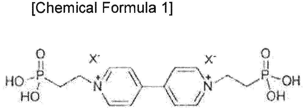


- In Chemical Formulae 1 to 7, X- is any one of BF4 -, ClO4 -, CF3SO3 -, F-, Cl-, Br-, and I-, and
- In Chemical Formula 7, R1 and R2 are any one of a methyl group, an ethyl group, a propyl group, a butyl group, a pentyl group, a hexyl group, a heptyl group, an octyl group, an isopentyl group, and a benzyl group.
- When a predetermined voltage is applied to the compounds represented by Chemical Formulae 1 to 7, the compounds are oxidized or reduced, and accordingly, the absorption spectra of the compounds are changed.
- For example, when voltage is applied to the compound (hereinafter, 'viologen') represented by Chemical Formula 7, the viologen is oxidized, and has a structure such as the following Chemical Formula 8. Accordingly, the absorption spectra of the compounds are changed, and the colors of the compounds are changed.

- The viologen may include various substituents, and the color and the discoloration potential according to the type of substituent are the same as those in the following Table 1.
[Table 1] Substituent (R1, R2) Color of Divalent Cation (MV2+) Color of Radical Cation (MV+?) Discoloration Potential (V)(vs SCE) Methyl colorless blue -0.688 Ethyl colorless blue -0.691 Propyl colorless blue -0.690 Butyl colorless blue -0.686 Pentyl colorless purple -0.686 Hexyl colorless I purple -0.710 Heptyl colorless mauve -0.600 Octyl colorless crimson -0.705 iso-Pentyl colorless purple -0.696 Benzyl colorless mauve -0.573 - Meanwhile, the organic material may be a polymer compound. Specifically, the polymer compound may be any one of polythiophene, poly(3-methylthiophene), polypyrrole, poly(3-methylketopyrrole), poly(3,4-dimethylpyrrole), poly(N-methylpyrrole), polyaniline, poly(2-methylaniline), and poly(3-methylaniline).
- The following Table 2 shows electrochromic characteristics of a polymer compound which uses thiophene and thiophene derivatives as monomers.
[Table 2] Type of polymer Absorption wavelength (nm) in oxidation state/Color Absorption wavelength (nm) in reduction state/Color Discoloration Potential (V)(vs SCE) Poly thiophene 730/blue 470/red 1.1 Poly(3-methylthiophene) 750/deep-blue 480/red 0.75 - The following Table 3 shows electrochromic characteristics of a polymer compound which uses pyrrole and pyrrole derivatives as monomers.
[Table 3] Type of polymer Color in oxidation state Color in reduction state Discoloration Potential (V)(vs SCE) Polypyrrole brown yellow 0 to 0.7 Poly(3-methylketopyrrole) yellow-brown brown-yellow 0 to 1.1 Poly(3.4-dimethylpyrrole) purple green -0.5 to 0.5 Poly(N-methylpyrrole) brown-red orange-yellow 0 to 0.8 - The following Table 4 shows electrochromic characteristics of a polymer compound which uses aniline and aniline derivatives as monomers.
[Table 4] Type of polymer -0.2 V absorption wavelength (nm) 0.2 V absorption wavelength (nm) 0.3 V absorption wavelength (nm) 0.4 V absorption wavelength (nm) -0.2 to 0.4 V response time (s) 0.4 to -0.20 V response time (s) Polyaniline 320, 440 320, 440, >820 330, 430, 800 340, 420, 800 1.4 0.6 Poly(2-methylaniline) 308, 420 308, 420 312, 410, >820 380, 800 1.6 0.6 Poly(3-methylaniline) 304, 420 304, 420 304, 410, >820 306, 390, >820 3.2 1.0 - Absorption spectra and discoloration potentials of the polymer compounds may vary depending on the molecular weight thereof without being limited to those in Tables 1 to 4.
- Meanwhile, when the second electrochromic material is formed of an inorganic material, the second electrochromic material may be formed at least one type of transition metal oxide. Specifically, the second electrochromic material may be formed of at least one of tungsten oxide, molybdenum oxide, tantalum oxide, niobium oxide, vanadium oxide, iron oxide, tin oxide, bismuth oxide, cerium oxide, manganese oxide, chromium oxide, cobalt oxide, rhodium oxide, iridium oxide, and nickel oxide.
- Here, the first electrochromic material and the second electrochromic material may be formed of different types of transition metal oxides.
- As described above, the nanoparticle according to the present invention may have both high light-shielding properties and a high electrochromic rate, and may have various colors.
- Meanwhile, the nanoparticle according to the present invention may be utilized by the method illustrated in
FIG. 2 . -
FIG. 2 is a conceptual view illustrating a structure of an electrochromic cell which utilizes the electrochromic nanoparticle according to the present invention. - As illustrated in
FIG. 2 , the electrochromic cell may be provided with adiscoloration layer 100 formed of the nanoparticles according to the present invention. Thediscoloration layer 100 is a layer in which a color is actually changed in the electrochromic cell. - In addition,
electrodes 210 for applying voltage to thediscoloration layer 100 are disposed at both sides of thediscoloration layer 100. When a voltage of a threshold or more is applied to theelectrodes 210, the color of thediscoloration layer 100 is changed while nanoparticles constituting thediscoloration layer 100 are oxidized or reduced. - In this case, the electrochromic cell may further include an
ion storage layer 220 for assisting the oxidation or reduction of the electrochromic material, anelectrolyte layer 230, and asealant layer 240. Here, theelectrolyte layer 230 may be a liquid phase, a solid phase, or a gel phase, and the type of material which may be constituted is shown in the following Table 5.[Table 5] Material Type LiClO4 propylene carbonate(PC) mixed w/ PMMA polymer complex amylopectin-rich starch (Amidex 4001), aqueous dispersion, mixed with glycerol or EG, addition of LiClO4, and dispersed in Teflon plaque polymer complex complex PVA w/ H3PO4, H2SO4, HCl polymer complex LiClO4, gelatin (Oetker), glycerol, formaldehyde polymer complex (p(TMC)/PEO)(poly(trimethylene carbonate)/poly(ethylene oxide)) doping w/ LiClO4 SPE p(TMC) w/ LiClO4 & LiBF4 SPE elastomer w/ LiClO4 polymer complex LiClO4, LiCF3SO3, LiN(CF3SO2)2polymer: PMMA, PEO, PVC, PANsolvent: PC, EC, γ-BL polymer complex PEO(polyethylene oxide) gel polymer UPON (lithium phosphorous oxynitride) inorganic P(VDF-TrFE) polar polymer polymer LiClO4 (d-U(2000)nLiClO4, d-U(900)nLiClO4)matrix: ormosils (organically modified silicates) from poly(oxyethylene) polymer complex LiF inorganic Ta2O5 inorganic LixTaOy inorganic LiClO4 in PC or PMMA+PC polymer complex PVA-H3PO4-PEG complex polymer complex LiPO4 + WO3 (2wt%) composite (LPWON) inorganic CuCl2 (cooper(II) chloride) + animal protein + gelatine polymer complex mica film, lithium fluorhectorite film LiClO4polymer : polypropylene carbonate, poly(epichlorohydrin-co-ethylene oxide) polymer complex HSbO32H2O inorganic Li salt, LPEI(linear poly(ethylene imine), PEO(poly(ethylene oxide) polymer complex HCI+PEO, PEO+LiClO4, PTS+urea+glycerol, PEO+PTS, PTS+glycerol+PEO polymer complex CSE (cellulose matrix solid electrolyte), NCC (nanocrystalline cellulose) cellulose type optimized BEMA/PEGMA, Li+ polymer (gel) HPC(hydroxypropyl cellulose) based, CH2Cl2 (dichloromethane), PEG, DBSA(4-dodecylbenzenesulfonic acid) cellulose based polymer (gel) - Meanwhile, the sealant layer serves to maintain the sealing and the cell gap.
- Meanwhile, the
ion storage layer 220 is only a constituent element for assisting the oxidation or reduction of the electrochromic material, and is not an essential constituent element of the electrochromic cell. - Meanwhile, the nanoparticle according to the present invention may further include at least one layer between a core and a shell.
-
FIG. 3 is a conceptual view illustrating an electrochromic nanoparticle further including an adsorption layer between a core and a shell. - As in
FIG. 3 , thenanoparticle 100 according to the present invention may further include anadsorption layer 310 formed between a core 110 and ashell 120 so as to enhance adsorption force of the core and the shell. In an Example, theadsorption layer 310 may be formed of TiO2. TiO2 is a transition metal oxide, but has weak electrochromic characteristics. Accordingly, TiO2 scarcely affects the absorption spectrum of thenanoparticle 100. However, TiO2 serves to increase bonding force of thecore 110 and theshell 120. Accordingly, the structural stability of thenanoparticle 100 according to the present invention is enhanced. - Hereinafter, the present invention will be described in more detail through the Examples and the Experimental Examples. However, the scope and content of the present invention are not interpreted to be curtailed or limited by the Examples and the Experimental Examples to be described below.
- The transmittance of a nanoparticle in which a core was formed of titanium oxide and a shell was formed of the compound (hereinafter, phenanthroline) represented by Chemical Formula 6 was measured at each wavelength. In this case, the wavelength band measured was 400 nm to 800 nm.
- Thereafter, voltage was applied to the nanoparticle, and the value of voltage applied was gradually increased. After the nanoparticle was discolored, the application of voltage was stopped, and the transmittance of the discolored nanoparticle was measured at each wavelength. In this case, the wavelength band measured was 400 nm to 800 nm.
-
FIG. 4A is a graph showing the transmittance of the nanoparticle used in Experimental Example 1 at each wavelength. -
FIG. 4A includes two graphs (first and second states), and the first state and the second state show the transmittance of the nanoparticle before the discoloration and the transmittance of the nanoparticle after the discoloration, respectively. According toFIG. 4A , the transmittance within a wavelength band of about 420 nm to about 510 nm after the nanoparticle was discolored was decreased. The nanoparticle used in Experimental Example 1 displayed a red-based color after the discoloration. - The transmittance of a nanoparticle in which a core was formed of tungsten oxide and a shell was formed of phenanthroline was measured at each wavelength. In this case, the wavelength band measured was 400 nm to 800 nm.
- Thereafter, voltage was applied to the nanoparticle, and the value of voltage applied was gradually increased. After the nanoparticle was discolored, the application of voltage was stopped, and the transmittance of the discolored nanoparticle was measured at each wavelength. In this case, the wavelength band measured was 400 nm to 800 nm.
-
FIG. 4B is a graph showing the transmittance of the nanoparticle used in Experimental Example 2 at each wavelength. -
FIG. 4B includes two graphs (first and second states), and the first state and the second state show the transmittance of the nanoparticle before the discoloration and the transmittance of the nanoparticle after the discoloration, respectively. According toFIG. 4B , after the nanoparticle was discolored, the transmittances within all the wavelength bands were rapidly decreased. - Specifically, as the nanoparticle is converted from the first state to the second state, the transmittance at each wavelength within a wavelength band of 400 nm to 800 nm was decreased to 0.06 to 0.6 times. Further, as the nanoparticle at a wavelength with a high transmittance was converted from the first state to the second state, the transmittance was decreased by a large margin.
- In addition, as the nanoparticle is converted from the first state to the second state, all the transmittances within a wavelength band of 400 nm to 800 nm were decreased to 30% or less. Accordingly, the nanoparticle used in Experimental Example 2 displayed a black-based color after the discoloration.
- The nanoparticles in Experimental Example 1 and Experimental Example 2 had the same constituent component of the shell, but it could be confirmed that the light transmittance (second mode) in Experimental Example 2 was much lower than the light transmittance (second mode) in Experimental Example 1.
- The transmittance of a nanoparticle in which a core was formed of tungsten oxide and a shell was formed of viologen was measured at each wavelength. In this case, the wavelength band measured was 400 nm to 800 nm.
- Thereafter, voltage was applied to the nanoparticle, and the value of voltage applied was gradually increased. After the nanoparticle was discolored, the application of voltage was stopped, and the transmittance of the discolored nanoparticle was measured at each wavelength. In this case, the wavelength band measured was 400 nm to 800 nm.
-
FIG. 4C is a graph showing the transmittance of the nanoparticle used in Experimental Example 3 at each wavelength. -
FIG. 4C includes two graphs (first and second states), and the first state and the second state show the transmittance of the nanoparticle before the discoloration and the transmittance of the nanoparticle after the discoloration, respectively. According toFIG. 4C , after the nanoparticle was discolored, the transmittance at a wavelength of about 600 nm to about 800 nm was rapidly decreased. - Specifically, as the nanoparticle was converted from the first state to the second state, the light transmittance at each wavelength within a wavelength band of 400 nm to 500 nm was decreased to 0.65 times to 0.80 times, and the light transmittance at each wavelength within a wavelength band of 500 nm to 800 nm was decreased to 0.20 times to 0.80 times.
- Further, as the nanoparticle was converted from the first state to the second state, the light transmittance at each wavelength within a wavelength band of 400 nm to 500 nm was changed from 15% to 60% to 10% to 50%, and the light transmittance at each wavelength within a wavelength band of 500 nm to 800 nm was changed from 60% to 80% to 17% to 50%.
- That is, the light transmittance at each wavelength within a wavelength band of 500 nm to 800 nm was decreased by a larger margin than that within a wavelength band of 400 nm to 500 nm. The nanoparticle used in Experimental Example 3 displayed a blue-based color after the discoloration.
- The aforementioned detailed description should not be interpreted as limitative in all aspects, and should be considered as illustrative. The scope of the present invention is defined by the claims.
Claims (9)
- An electrochromic nanoparticle comprising:a core formed of a first electrochromic material; anda shell encompassing the core and formed of a second electrochromic material, wherein the first electrochromic material is formed of at least one type of transition metal oxide, and the second electrochromic material is formed of an organic material or at least one type of transition metal oxide that is different from the at least one type of transition metal oxide of the first electrochromic material,wherein when a voltage equal to or more than a reference value is applied to the nanoparticles, the nanoparticle is converted from a first state to a second state, and when a reverse voltage equal to or more than the reference value is applied to the nanoparticle in the second state, the nanoparticle is converted from the second state to the first state, and the nanoparticle has different light transmittances in the first and second states,wherein the first electrochromic material and the second electrochromic material in the second state each have a color,characterized in that the second electrochromic material has a complementary color to that of the first electrochromic material in the second state.
- The electrochromic nanoparticle of claim 1, wherein when the nanoparticle is converted from the first state to the second state, the light transmittance at each wavelength within a wavelength band of 400 nm to 800 nm is decreased to 0.06 times to 0.6 times.
- The electrochromic nanoparticle according to claim 1 or 2, wherein the light transmittance of the nanoparticle in the first state at each wavelength within a wavelength band of 400 nm to 800 nm is 15% to 90%, and the light transmittance of the nanoparticle in the second state at each wavelength within a wavelength band of 400 nm to 800 nm is 5% to 30%.
- The electrochromic nanoparticle according to any one of claims 1 to 3, wherein the light transmittance of the nanoparticle in the first state at each wavelength is 15% to 60% within a wavelength band of 400 nm to 500 nm and 60% to 80% within a wavelength band of 500 nm to 800 nm, and the light transmittance of the nanoparticle in the second state at each wavelength is 10% to 50% within a wavelength band of 400 nm to 500 nm and 17% to 50% within a wavelength band of 500 nm to 800 nm.
- The electrochromic nanoparticle according to any one of claims 1 to 4,
wherein the first electrochromic material is formed of at least one of tungsten oxide, molybdenum oxide, tantalum oxide, niobium oxide, vanadium oxide, iron oxide, manganese oxide, chromium oxide, cobalt oxide, rhodium oxide, iridium oxide, and nickel oxide. - The electrochromic nanoparticle according to any one of claims 1 to 5,
wherein the organic material forming the second electrochromic material is any one of compounds represented by the following Chemical Formulae 1 to 7.


in Chemical Formula 7, R1 and R2 are any one of a methyl group, an ethyl group, a propyl group, a butyl group, a pentyl group, a hexyl group, a heptyl group, an octyl group, an isopentyl group, and a benzyl group. - The electrochromic nanoparticle according to any one of claims 1 to 6,
wherein the organic material forming the second electrochromic material is any one of polythiophene, poly(3-methylthiophene), polypyrrole, poly(3-methylketopyrrole), poly(3,4-dimethylpyrrole), poly(N-methylpyrrole), polyaniline, poly(2-methylaniline), and poly(3-methylaniline). - The electrochromic nanoparticle according to any one of claims 1 to 7, further comprising an adsorption layer positioned between the core and the shell and formed so as to enhance adsorption force of the core and the shell.
- The electrochromic nanoparticle of claim 8, wherein the adsorption layer is formed of TiO2.
Applications Claiming Priority (2)
| Application Number | Priority Date | Filing Date | Title |
|---|---|---|---|
| KR1020160027088A KR102578032B1 (en) | 2016-03-07 | 2016-03-07 | Electrochromic nanoparticle |
| PCT/KR2016/002636 WO2017155146A1 (en) | 2016-03-07 | 2016-03-16 | Electrochromic nanoparticle |
Publications (3)
| Publication Number | Publication Date |
|---|---|
| EP3428243A1 EP3428243A1 (en) | 2019-01-16 |
| EP3428243A4 EP3428243A4 (en) | 2019-08-28 |
| EP3428243B1 true EP3428243B1 (en) | 2021-02-17 |
Family
ID=59790502
Family Applications (1)
| Application Number | Title | Priority Date | Filing Date |
|---|---|---|---|
| EP16893661.5A Active EP3428243B1 (en) | 2016-03-07 | 2016-03-16 | Electrochromic nanoparticle |
Country Status (5)
| Country | Link |
|---|---|
| US (1) | US11307474B2 (en) |
| EP (1) | EP3428243B1 (en) |
| KR (1) | KR102578032B1 (en) |
| CN (1) | CN108699430A (en) |
| WO (1) | WO2017155146A1 (en) |
Families Citing this family (9)
| Publication number | Priority date | Publication date | Assignee | Title |
|---|---|---|---|---|
| KR102086689B1 (en) | 2018-02-06 | 2020-03-09 | 주식회사 진씨커 | Kit for isolation of mutant cell free DNA and method for isolation of mutant cell free DNA using the same |
| CN108549185A (en) * | 2018-06-01 | 2018-09-18 | Oppo广东移动通信有限公司 | Shell and preparation method, electronic equipment |
| CN108761950A (en) * | 2018-06-01 | 2018-11-06 | Oppo广东移动通信有限公司 | Shell and preparation method, electronic equipment |
| US12044963B2 (en) * | 2020-01-22 | 2024-07-23 | Applied Materials, Inc. | High refractive index imprint compositions and materials and processes for making the same |
| KR102522644B1 (en) * | 2020-08-13 | 2023-04-18 | (주)오리온엔이에스 | Electrochromic device having dispersed chromic complex object with core-shell structure |
| WO2022108922A1 (en) * | 2020-11-18 | 2022-05-27 | Applied Materials, Inc. | Imprint compositions with passivated nanoparticles and materials and processes for making the same |
| US11873232B2 (en) | 2020-12-01 | 2024-01-16 | Electronics And Telecommunications Research Institute | Method for producing hexagonal tungsten oxide and method for producing electrochromic device including the same |
| CN116808204B (en) * | 2023-05-16 | 2025-12-16 | 桂林电子科技大学 | PPy@CeO2NPs nano particle and preparation method and application thereof |
| KR20250172028A (en) | 2024-05-31 | 2025-12-09 | (주)오리온엔이에스 | A photochromic device with improved durability and method ofmanufacturing the same |
Family Cites Families (7)
| Publication number | Priority date | Publication date | Assignee | Title |
|---|---|---|---|---|
| US5413739A (en) * | 1992-12-22 | 1995-05-09 | Coleman; James P. | Electrochromic materials and displays |
| EP1443090A1 (en) * | 2003-01-31 | 2004-08-04 | Ntera Limited | Electrochromic particles |
| US20080128665A1 (en) * | 2006-12-04 | 2008-06-05 | 3M Innovative Properties Company | Nanoparticle based thin films |
| KR102001887B1 (en) | 2012-08-28 | 2019-07-19 | 엘지디스플레이 주식회사 | Electro chromic particle and display device comprising of the same |
| KR101947071B1 (en) | 2013-04-30 | 2019-02-12 | 엘지디스플레이 주식회사 | Light Shutter Particle And Method Manufacturing The Same, And Reflective Type Display Device Using The Same |
| CN103469272B (en) * | 2013-09-04 | 2015-11-25 | 浙江大学 | Tungsten trioxide/polyanilinecore-shell core-shell nanowire array radiochromic film and preparation method thereof |
| CN104609705A (en) | 2015-01-23 | 2015-05-13 | 天津城建大学 | Preparation method of WO3-TiO2 core-shell structure electrochromic glass |
-
2016
- 2016-03-07 KR KR1020160027088A patent/KR102578032B1/en active Active
- 2016-03-16 US US16/077,197 patent/US11307474B2/en active Active
- 2016-03-16 CN CN201680083111.0A patent/CN108699430A/en active Pending
- 2016-03-16 EP EP16893661.5A patent/EP3428243B1/en active Active
- 2016-03-16 WO PCT/KR2016/002636 patent/WO2017155146A1/en not_active Ceased
Non-Patent Citations (1)
| Title |
|---|
| None * |
Also Published As
| Publication number | Publication date |
|---|---|
| EP3428243A1 (en) | 2019-01-16 |
| CN108699430A (en) | 2018-10-23 |
| WO2017155146A1 (en) | 2017-09-14 |
| KR20170104269A (en) | 2017-09-15 |
| US20200089073A1 (en) | 2020-03-19 |
| US11307474B2 (en) | 2022-04-19 |
| EP3428243A4 (en) | 2019-08-28 |
| KR102578032B1 (en) | 2023-09-13 |
Similar Documents
| Publication | Publication Date | Title |
|---|---|---|
| EP3428243A1 (en) | Electrochromic nanoparticle | |
| Lu et al. | An electrochromic device based on Prussian blue, self-immobilized vinyl benzyl viologen, and ferrocene | |
| Thakur et al. | Hybrid materials and polymer electrolytes for electrochromic device applications | |
| JP4670948B2 (en) | Display medium and display device | |
| US9933680B2 (en) | Heat-resistant electrolyte materials and electrochromic devices including them | |
| US20120127554A1 (en) | Display device and color electronic paper using the same | |
| Hu et al. | High contrast all-solid-state electrochromic device with 2, 2, 6, 6-tetramethyl-1-piperidinyloxy (TEMPO), heptyl viologen, and succinonitrile | |
| Thi-Thanh-Nhi et al. | A gel-based electrochromic device towards fast response and high coloration efficiency for low-power consumption smart window applications | |
| Dulgerbaki et al. | Efficient electrochromic materials based on PEDOT/WO3 composites synthesized in ionic liquid media | |
| Medrano-Solís et al. | Study of dual electrochromic devices based on polyaniline and poly (3-hexylthiophene) thin films | |
| Huang et al. | Spectroelectrochemical and adhesion properties of chemically synthesized ion conducting poly (vinyl butyral) in Prussian blue and poly (3, 4-ethylenedioxythiophene) laminated electrochromic glazing | |
| JPWO2009031422A1 (en) | Method for manufacturing electrochromic display element | |
| KR20180129161A (en) | Electrochromism element | |
| JP3464513B2 (en) | All-solid-state electrochromic device and method of manufacturing the same | |
| JP6056361B2 (en) | Electrochromic display element | |
| KR101857051B1 (en) | Electrochromic electrode film comprising grephene oxide protecting layer, method for preparing the same and electrochromic device comprising the same | |
| Chang et al. | Incorporation of plastic crystal and transparent UV-cured polymeric electrolyte in a complementary electrochromic device | |
| JP5630248B2 (en) | Electrochromic display element | |
| JP6234427B2 (en) | Organic compound, light modulation composition, and light modulation device using the same | |
| JP2003161963A (en) | Electrochromic element | |
| JP2016218357A (en) | Driving method of electrochromic device and electrochromic device | |
| JP2016218358A (en) | Electrochromic device driving method and electrochromic device | |
| JP2007298713A (en) | Electrochromic display | |
| Onoda et al. | Properties and applications for electronics of poly (isothianaphthene) | |
| KR100882111B1 (en) | Electrolyte for Electrochromic Device |
Legal Events
| Date | Code | Title | Description |
|---|---|---|---|
| STAA | Information on the status of an ep patent application or granted ep patent |
Free format text: STATUS: THE INTERNATIONAL PUBLICATION HAS BEEN MADE |
|
| PUAI | Public reference made under article 153(3) epc to a published international application that has entered the european phase |
Free format text: ORIGINAL CODE: 0009012 |
|
| STAA | Information on the status of an ep patent application or granted ep patent |
Free format text: STATUS: REQUEST FOR EXAMINATION WAS MADE |
|
| 17P | Request for examination filed |
Effective date: 20180816 |
|
| AK | Designated contracting states |
Kind code of ref document: A1 Designated state(s): AL AT BE BG CH CY CZ DE DK EE ES FI FR GB GR HR HU IE IS IT LI LT LU LV MC MK MT NL NO PL PT RO RS SE SI SK SM TR |
|
| AX | Request for extension of the european patent |
Extension state: BA ME |
|
| DAV | Request for validation of the european patent (deleted) | ||
| DAX | Request for extension of the european patent (deleted) | ||
| A4 | Supplementary search report drawn up and despatched |
Effective date: 20190731 |
|
| RIC1 | Information provided on ipc code assigned before grant |
Ipc: G02F 1/15 20190101ALI20190725BHEP Ipc: C09K 9/02 20060101ALI20190725BHEP Ipc: C09K 9/00 20060101AFI20190725BHEP |
|
| STAA | Information on the status of an ep patent application or granted ep patent |
Free format text: STATUS: EXAMINATION IS IN PROGRESS |
|
| 17Q | First examination report despatched |
Effective date: 20200205 |
|
| GRAP | Despatch of communication of intention to grant a patent |
Free format text: ORIGINAL CODE: EPIDOSNIGR1 |
|
| STAA | Information on the status of an ep patent application or granted ep patent |
Free format text: STATUS: GRANT OF PATENT IS INTENDED |
|
| RIC1 | Information provided on ipc code assigned before grant |
Ipc: G02F 1/1514 20190101ALI20200930BHEP Ipc: G02F 1/1503 20190101ALI20200930BHEP Ipc: C09K 9/00 20060101AFI20200930BHEP Ipc: C09K 9/02 20060101ALI20200930BHEP |
|
| INTG | Intention to grant announced |
Effective date: 20201029 |
|
| GRAS | Grant fee paid |
Free format text: ORIGINAL CODE: EPIDOSNIGR3 |
|
| GRAA | (expected) grant |
Free format text: ORIGINAL CODE: 0009210 |
|
| STAA | Information on the status of an ep patent application or granted ep patent |
Free format text: STATUS: THE PATENT HAS BEEN GRANTED |
|
| REG | Reference to a national code |
Ref country code: DE Ref legal event code: R082 Ref document number: 602016052892 Country of ref document: DE Representative=s name: WUESTHOFF & WUESTHOFF, PATENTANWAELTE PARTG MB, DE |
|
| AK | Designated contracting states |
Kind code of ref document: B1 Designated state(s): AL AT BE BG CH CY CZ DE DK EE ES FI FR GB GR HR HU IE IS IT LI LT LU LV MC MK MT NL NO PL PT RO RS SE SI SK SM TR |
|
| REG | Reference to a national code |
Ref country code: GB Ref legal event code: FG4D |
|
| REG | Reference to a national code |
Ref country code: CH Ref legal event code: EP |
|
| REG | Reference to a national code |
Ref country code: DE Ref legal event code: R096 Ref document number: 602016052892 Country of ref document: DE |
|
| REG | Reference to a national code |
Ref country code: AT Ref legal event code: REF Ref document number: 1361445 Country of ref document: AT Kind code of ref document: T Effective date: 20210315 |
|
| REG | Reference to a national code |
Ref country code: IE Ref legal event code: FG4D |
|
| REG | Reference to a national code |
Ref country code: LT Ref legal event code: MG9D |
|
| REG | Reference to a national code |
Ref country code: NL Ref legal event code: MP Effective date: 20210217 |
|
| PG25 | Lapsed in a contracting state [announced via postgrant information from national office to epo] |
Ref country code: LT Free format text: LAPSE BECAUSE OF FAILURE TO SUBMIT A TRANSLATION OF THE DESCRIPTION OR TO PAY THE FEE WITHIN THE PRESCRIBED TIME-LIMIT Effective date: 20210217 Ref country code: BG Free format text: LAPSE BECAUSE OF FAILURE TO SUBMIT A TRANSLATION OF THE DESCRIPTION OR TO PAY THE FEE WITHIN THE PRESCRIBED TIME-LIMIT Effective date: 20210517 Ref country code: HR Free format text: LAPSE BECAUSE OF FAILURE TO SUBMIT A TRANSLATION OF THE DESCRIPTION OR TO PAY THE FEE WITHIN THE PRESCRIBED TIME-LIMIT Effective date: 20210217 Ref country code: GR Free format text: LAPSE BECAUSE OF FAILURE TO SUBMIT A TRANSLATION OF THE DESCRIPTION OR TO PAY THE FEE WITHIN THE PRESCRIBED TIME-LIMIT Effective date: 20210518 Ref country code: FI Free format text: LAPSE BECAUSE OF FAILURE TO SUBMIT A TRANSLATION OF THE DESCRIPTION OR TO PAY THE FEE WITHIN THE PRESCRIBED TIME-LIMIT Effective date: 20210217 Ref country code: PT Free format text: LAPSE BECAUSE OF FAILURE TO SUBMIT A TRANSLATION OF THE DESCRIPTION OR TO PAY THE FEE WITHIN THE PRESCRIBED TIME-LIMIT Effective date: 20210617 Ref country code: NO Free format text: LAPSE BECAUSE OF FAILURE TO SUBMIT A TRANSLATION OF THE DESCRIPTION OR TO PAY THE FEE WITHIN THE PRESCRIBED TIME-LIMIT Effective date: 20210517 |
|
| REG | Reference to a national code |
Ref country code: AT Ref legal event code: MK05 Ref document number: 1361445 Country of ref document: AT Kind code of ref document: T Effective date: 20210217 |
|
| PG25 | Lapsed in a contracting state [announced via postgrant information from national office to epo] |
Ref country code: SE Free format text: LAPSE BECAUSE OF FAILURE TO SUBMIT A TRANSLATION OF THE DESCRIPTION OR TO PAY THE FEE WITHIN THE PRESCRIBED TIME-LIMIT Effective date: 20210217 Ref country code: NL Free format text: LAPSE BECAUSE OF FAILURE TO SUBMIT A TRANSLATION OF THE DESCRIPTION OR TO PAY THE FEE WITHIN THE PRESCRIBED TIME-LIMIT Effective date: 20210217 Ref country code: PL Free format text: LAPSE BECAUSE OF FAILURE TO SUBMIT A TRANSLATION OF THE DESCRIPTION OR TO PAY THE FEE WITHIN THE PRESCRIBED TIME-LIMIT Effective date: 20210217 Ref country code: LV Free format text: LAPSE BECAUSE OF FAILURE TO SUBMIT A TRANSLATION OF THE DESCRIPTION OR TO PAY THE FEE WITHIN THE PRESCRIBED TIME-LIMIT Effective date: 20210217 Ref country code: RS Free format text: LAPSE BECAUSE OF FAILURE TO SUBMIT A TRANSLATION OF THE DESCRIPTION OR TO PAY THE FEE WITHIN THE PRESCRIBED TIME-LIMIT Effective date: 20210217 |
|
| PG25 | Lapsed in a contracting state [announced via postgrant information from national office to epo] |
Ref country code: IS Free format text: LAPSE BECAUSE OF FAILURE TO SUBMIT A TRANSLATION OF THE DESCRIPTION OR TO PAY THE FEE WITHIN THE PRESCRIBED TIME-LIMIT Effective date: 20210617 |
|
| PG25 | Lapsed in a contracting state [announced via postgrant information from national office to epo] |
Ref country code: AT Free format text: LAPSE BECAUSE OF FAILURE TO SUBMIT A TRANSLATION OF THE DESCRIPTION OR TO PAY THE FEE WITHIN THE PRESCRIBED TIME-LIMIT Effective date: 20210217 Ref country code: SM Free format text: LAPSE BECAUSE OF FAILURE TO SUBMIT A TRANSLATION OF THE DESCRIPTION OR TO PAY THE FEE WITHIN THE PRESCRIBED TIME-LIMIT Effective date: 20210217 Ref country code: CZ Free format text: LAPSE BECAUSE OF FAILURE TO SUBMIT A TRANSLATION OF THE DESCRIPTION OR TO PAY THE FEE WITHIN THE PRESCRIBED TIME-LIMIT Effective date: 20210217 Ref country code: EE Free format text: LAPSE BECAUSE OF FAILURE TO SUBMIT A TRANSLATION OF THE DESCRIPTION OR TO PAY THE FEE WITHIN THE PRESCRIBED TIME-LIMIT Effective date: 20210217 |
|
| REG | Reference to a national code |
Ref country code: CH Ref legal event code: PL |
|
| REG | Reference to a national code |
Ref country code: DE Ref legal event code: R097 Ref document number: 602016052892 Country of ref document: DE |
|
| PG25 | Lapsed in a contracting state [announced via postgrant information from national office to epo] |
Ref country code: RO Free format text: LAPSE BECAUSE OF FAILURE TO SUBMIT A TRANSLATION OF THE DESCRIPTION OR TO PAY THE FEE WITHIN THE PRESCRIBED TIME-LIMIT Effective date: 20210217 Ref country code: SK Free format text: LAPSE BECAUSE OF FAILURE TO SUBMIT A TRANSLATION OF THE DESCRIPTION OR TO PAY THE FEE WITHIN THE PRESCRIBED TIME-LIMIT Effective date: 20210217 Ref country code: MC Free format text: LAPSE BECAUSE OF FAILURE TO SUBMIT A TRANSLATION OF THE DESCRIPTION OR TO PAY THE FEE WITHIN THE PRESCRIBED TIME-LIMIT Effective date: 20210217 Ref country code: DK Free format text: LAPSE BECAUSE OF FAILURE TO SUBMIT A TRANSLATION OF THE DESCRIPTION OR TO PAY THE FEE WITHIN THE PRESCRIBED TIME-LIMIT Effective date: 20210217 |
|
| REG | Reference to a national code |
Ref country code: BE Ref legal event code: MM Effective date: 20210331 |
|
| PLBE | No opposition filed within time limit |
Free format text: ORIGINAL CODE: 0009261 |
|
| STAA | Information on the status of an ep patent application or granted ep patent |
Free format text: STATUS: NO OPPOSITION FILED WITHIN TIME LIMIT |
|
| 26N | No opposition filed |
Effective date: 20211118 |
|
| GBPC | Gb: european patent ceased through non-payment of renewal fee |
Effective date: 20210517 |
|
| PG25 | Lapsed in a contracting state [announced via postgrant information from national office to epo] |
Ref country code: LI Free format text: LAPSE BECAUSE OF NON-PAYMENT OF DUE FEES Effective date: 20210331 Ref country code: LU Free format text: LAPSE BECAUSE OF NON-PAYMENT OF DUE FEES Effective date: 20210316 Ref country code: AL Free format text: LAPSE BECAUSE OF FAILURE TO SUBMIT A TRANSLATION OF THE DESCRIPTION OR TO PAY THE FEE WITHIN THE PRESCRIBED TIME-LIMIT Effective date: 20210217 Ref country code: CH Free format text: LAPSE BECAUSE OF NON-PAYMENT OF DUE FEES Effective date: 20210331 Ref country code: IE Free format text: LAPSE BECAUSE OF NON-PAYMENT OF DUE FEES Effective date: 20210316 Ref country code: FR Free format text: LAPSE BECAUSE OF NON-PAYMENT OF DUE FEES Effective date: 20210417 Ref country code: ES Free format text: LAPSE BECAUSE OF FAILURE TO SUBMIT A TRANSLATION OF THE DESCRIPTION OR TO PAY THE FEE WITHIN THE PRESCRIBED TIME-LIMIT Effective date: 20210217 |
|
| PG25 | Lapsed in a contracting state [announced via postgrant information from national office to epo] |
Ref country code: SI Free format text: LAPSE BECAUSE OF FAILURE TO SUBMIT A TRANSLATION OF THE DESCRIPTION OR TO PAY THE FEE WITHIN THE PRESCRIBED TIME-LIMIT Effective date: 20210217 |
|
| PG25 | Lapsed in a contracting state [announced via postgrant information from national office to epo] |
Ref country code: IT Free format text: LAPSE BECAUSE OF FAILURE TO SUBMIT A TRANSLATION OF THE DESCRIPTION OR TO PAY THE FEE WITHIN THE PRESCRIBED TIME-LIMIT Effective date: 20210217 Ref country code: GB Free format text: LAPSE BECAUSE OF NON-PAYMENT OF DUE FEES Effective date: 20210517 |
|
| PG25 | Lapsed in a contracting state [announced via postgrant information from national office to epo] |
Ref country code: IS Free format text: LAPSE BECAUSE OF FAILURE TO SUBMIT A TRANSLATION OF THE DESCRIPTION OR TO PAY THE FEE WITHIN THE PRESCRIBED TIME-LIMIT Effective date: 20210617 |
|
| PG25 | Lapsed in a contracting state [announced via postgrant information from national office to epo] |
Ref country code: BE Free format text: LAPSE BECAUSE OF NON-PAYMENT OF DUE FEES Effective date: 20210331 |
|
| PG25 | Lapsed in a contracting state [announced via postgrant information from national office to epo] |
Ref country code: CY Free format text: LAPSE BECAUSE OF FAILURE TO SUBMIT A TRANSLATION OF THE DESCRIPTION OR TO PAY THE FEE WITHIN THE PRESCRIBED TIME-LIMIT Effective date: 20210217 |
|
| PG25 | Lapsed in a contracting state [announced via postgrant information from national office to epo] |
Ref country code: HU Free format text: LAPSE BECAUSE OF FAILURE TO SUBMIT A TRANSLATION OF THE DESCRIPTION OR TO PAY THE FEE WITHIN THE PRESCRIBED TIME-LIMIT; INVALID AB INITIO Effective date: 20160316 |
|
| PG25 | Lapsed in a contracting state [announced via postgrant information from national office to epo] |
Ref country code: MK Free format text: LAPSE BECAUSE OF FAILURE TO SUBMIT A TRANSLATION OF THE DESCRIPTION OR TO PAY THE FEE WITHIN THE PRESCRIBED TIME-LIMIT Effective date: 20210217 |
|
| PG25 | Lapsed in a contracting state [announced via postgrant information from national office to epo] |
Ref country code: TR Free format text: LAPSE BECAUSE OF FAILURE TO SUBMIT A TRANSLATION OF THE DESCRIPTION OR TO PAY THE FEE WITHIN THE PRESCRIBED TIME-LIMIT Effective date: 20210217 |
|
| PG25 | Lapsed in a contracting state [announced via postgrant information from national office to epo] |
Ref country code: MT Free format text: LAPSE BECAUSE OF FAILURE TO SUBMIT A TRANSLATION OF THE DESCRIPTION OR TO PAY THE FEE WITHIN THE PRESCRIBED TIME-LIMIT Effective date: 20210217 |
|
| PGFP | Annual fee paid to national office [announced via postgrant information from national office to epo] |
Ref country code: DE Payment date: 20260205 Year of fee payment: 11 |