EP3426004A1 - Driver for light source with selectable output current - Google Patents
Driver for light source with selectable output current Download PDFInfo
- Publication number
- EP3426004A1 EP3426004A1 EP17180295.2A EP17180295A EP3426004A1 EP 3426004 A1 EP3426004 A1 EP 3426004A1 EP 17180295 A EP17180295 A EP 17180295A EP 3426004 A1 EP3426004 A1 EP 3426004A1
- Authority
- EP
- European Patent Office
- Prior art keywords
- driver device
- circuit board
- delineated
- current
- current path
- Prior art date
- Legal status (The legal status is an assumption and is not a legal conclusion. Google has not performed a legal analysis and makes no representation as to the accuracy of the status listed.)
- Withdrawn
Links
Images
Classifications
-
- H—ELECTRICITY
- H05—ELECTRIC TECHNIQUES NOT OTHERWISE PROVIDED FOR
- H05B—ELECTRIC HEATING; ELECTRIC LIGHT SOURCES NOT OTHERWISE PROVIDED FOR; CIRCUIT ARRANGEMENTS FOR ELECTRIC LIGHT SOURCES, IN GENERAL
- H05B45/00—Circuit arrangements for operating light-emitting diodes [LED]
- H05B45/30—Driver circuits
- H05B45/37—Converter circuits
- H05B45/3725—Switched mode power supply [SMPS]
Definitions
- the invention relates to setting the output characteristics of a driver device for semiconductor light sources, such as LEDs.
- the invention relates to making such setting easy and straightforward at the stage of assembling a luminaire or otherwise finalising the combination of the various components that constitute the luminaire.
- Luminaires that employ semiconductor light sources such as LEDs need a driver device that feeds the available electric power to the LEDs at suitable voltage and current levels.
- the raw electric power is AC mains at for example 230 V and 50 Hz.
- the output voltage of the driver device may be fixed DC at for example 12 V or 24 V, or it may be allowed to vary within a certain range so that it will meet the sum of forward threshold voltages of the LEDs connected in series across the output.
- the output current may be fixed at a suitable value, such as e.g. 350 mA, 700 mA, or 1050 mA, or it may be controllable to allow dimming the LEDs.
- a typical driver device comprises circuit elements such as rectifiers, filters, and one or more switched-mode converters to accomplish its task.
- a driver device should be as simple as possible to keep the manufacturing costs under control.
- the manufacturer of LED luminaires wants to produce luminaires with different designs, different number and type of LEDs, and/or different amounts of produced light. Trying to fulfil all needs may lead to a relatively complicated matrix of decisions, where the luminaire manufacturer must either acquire complicated (and expensive) controllable drivers or stock a considerable variety of constant output drivers, trying to constantly meet the rapidly varying needs of his manufacturing lines.
- a compromise with some important advantages involves the use of drivers with settable output characteristics.
- a driver device exhibits a two-pole connector, to which the luminaire manufacturer can attach a resistor of selected magnitude.
- the resistor becomes a part of the current feedback circuit of the driver device, with the effect that the output current will be set at a corresponding fixed value or range.
- a so-called Iset resistor of this kind may set the fixed output current level of a constant current driver, or it may set the upper limit of the output current range of a controllable driver.
- the selected resistance of the externally connected resistor may set the output voltage, PWM frequency, or other output characteristic of the driver device.
- a circuit board of the driver device comprise one or more portions that can be easily snapped or cut off, so that removing those components and/or conductive track portions from the driver circuit that appeared on the removed portions of the circuit board has a desired effect on output characteristics.
- a driver device for semiconductor light sources.
- the driver device comprises a circuit board and electronic components and conductive tracks attached to and supported by said circuit board.
- the circuit board comprises a delineated portion through which goes at least one current path consisting of some of said conductive tracks and electronic components, the electric conductivity of said current path having an effect on output characteristics of said driver device.
- the structural strength of the circuit board is weakened at the border of said delineated portion for allowing controllable removal of said delineated portion without damaging the rest of the circuit board.
- a method for setting the output characteristics of a driver for semiconductor light sources comprises breaking off a delineated portion of a circuit board of the driver device along a weakened border of said delineated portion, said delineated portion carrying a current path that is connected to at least some of the electronic components and conductive tracks on the rest of the circuit board.
- the invention is related to driving semiconductor light sources, such as LEDs, OLEDs, laser diodes, or the like.
- LEDs such as LEDs, OLEDs, laser diodes, or the like.
- LEDs are often used while the meaning is not to limit the discussion to just LEDs in a narrow sense but to semiconductor light sources in general.
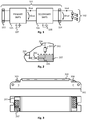
- Fig. 1 illustrates schematically a driver device 101 for semiconductor light sources 102, which are illustrated in the form of LEDs.
- the driver device comprises a power input 103 and a LED current output 104.
- the power input 103 is typically meant to be coupled to AC mains.
- One or more switched-mode converter stages are provided for converting the energy drawn by the power input 103 into a voltage and current that can be provided at the LED current output 104 to make the semiconductor light sources 102 shine at a desired brightness.
- the driver device 101 comprises a primary switched-mode converter stage 105 and a secondary switched-mode converter stage 106 coupled in series between the power input 103 and the LED current output 104.
- the primary switched-mode converter stage 105 is configured to perform PFC (power factor correction) and to produce a so-called internal bus voltage Vbus, which constitutes the input voltage to the secondary switched-mode converter stage 106.
- the secondary switched-mode converter stage 106 is configured to draw a current Ibus and to produce the output voltage Vout, which feeds an output current lout through the semiconductor light sources 102.
- Such a two-stage structure of a driver device, as well as the tasks and operating principles of the two switched-mode converter stages, are as such well known to the person skilled in the art and they do not need to be discussed further.
- Fig. 1 illustrates schematically a corner of a circuit board 201, with electronic components 202 and 203 as well as conductive tracks 204, 205, and 206 attached to and supported by the circuit board.
- the circuit board 201 comprises also a delineated portion 207, through which goes at least one current path that consists of some of the conductive tracks and electronic components.
- the electronic components 202 and 203 as well as the conductive track 206 are parts of such a current path.
- the hatched pattern appears in fig. 2 only to graphically demonstrate the delineated portion 207, and it does not need to appear in any tangible form on the actual circuit board.
- the structural strength of the circuit board is deliberately weakened at the border of the delineated portion 207.
- the weakening is accomplished by making perforated lines appear in the circuit board material along the border of the delineated portion 207.
- the weakening would allow controllable removal of the delineated portion 207 without damaging the rest of the circuit board.
- the delineated portion 207 could be snapped off simply by bending it along the perforated lines, or a pair of cutoff pliers could be used to cut the delineated portion 207 out. Removing the delineated portion 207 would cut the current path that consists of the electronic components 202 and 203 and the conductive track 206.
- circuit board material is susceptible to local structural weakening through localized thermal treatment, like momentarily bringing a very hot and sharp object into contact with a selected point or line on the circuit board, such treatment can be used for causing the desired structural weakening.
- a tightly focused beam of electromagnetic radiation, fluid, or fine particles can interact with the circuit board material, causing local structural weakening.
- said current path is part of the primary switched-mode converter stage 105, or part of the secondary switched-mode converter stage 106.
- the first alternative is illustrated schematically as the severable current path 107
- the second alternative is illustrated schematically as the severable current path 108.
- the circuit board on which the driver device 101 is built comprises two delineated portions of the kind described above (or a first circuit board on which the primary switched-mode converter stage 105 is built comprises one delineated portion and a second circuit board on which the secondary switched-mode converter stage 106 is built comprises another delineated portion), so that the current path going through one of the delineated portions is part of the primary switched-mode converter stage 105 and the current path going through the other of the delineated portions is part of the secondary switched-mode converter stage 106.
- the electric conductivity of the current path has an effect on the output characteristics of the driver device: controllably removing the delineated portion of the circuit board causes a change in the electric conductivity of the current path, which in turn causes a change in the output characteristics.
- a change in its electric conductivity may have an effect on the internal bus voltage Vbus or the current Ibus, which may in turn affect the operation of the secondary switched-mode converter stage 106.
- the effect on the output characteristics of the driver device is somewhat indirect. A more direct effect may result if the current path is part of the secondary switched-mode converter stage 106, like current path 108 in fig. 1 .
- the current path in question is part of a feedback arrangement through which the secondary switched-mode converter stage 106 provides feedback to the primary switched-mode converter stage 105. In such a case the current path in question may even be said to be part of both the primary and secondary switched-mode converter stages.
- a driver device may comprise a closed outer cover that encloses a majority portion of the circuit board. It is advantageous if the delineated portion of the circuit board is visible and accessible outside the outer cover of the driver device, because this will facilitate making the desired change in the output characteristics of the driver device without opening its outer cover.
- driver devices are categorized as "linear” or “compact” devices according to their form factor: a linear driver device inherits its form factor from known electronic ballasts of fluorescent tube luminaires, so that the driver device is eye-catchingly elongated in form, while the relative dimensions of a compact device resemble those of a cigarette box.
- the driver device in fig. 3 is an example of one having the form factor of a linear driver device, but the following considerations are easily generalized to cover also compact-formed driver devices.
- the driver device is shown in a side view (upper part of fig. 3 ) and a top view (lower part of fig. 3 ). It comprises an elongated outer cover that consists of a base part 301 and a top part 302.
- the circuit board 201 has an elongated form in order to fit inside the outer cover, which enclosed a majority portion of the circuit board 201 but leaves both ends of the circuit board 201 visible and accessible.
- the driver device of fig. 3 has one delineated portion 207 of the kind described above located at one end of the circuit board, next to the connector 303.
- the component(s) and/or conductive track(s) of the current path going through the delineated portion 207 are not shown in fig. 3 ; they may be for example on that side of the circuit board 201 that is against the inner surface of the base part 301.
- An elongated driver device of this kind could comprise two delineated portions of the kind described above, for example one at each end of the circuit board.
- the delineated portion could also be located next to the connector. If there are two delineated portions, they could be located for example at both sides of the connector arrangement in order to easily distinguish between them. As such there is no imperative reason why a delineated portion should be just next to a connector or connector arrangement, but since both a connector and a delineated portion benefit from being visible and easily accessible, and since the outer cover of a driver device typically leaves a relatively small proportion of the circuit board visible and accessible, in many cases the side by side placement of the connector and the delineated portion works well as a solution.
- the delineated portion was not accessible without opening the outer cover of the driver device, it may be advantageous to make it visible for example by making an opening in the outer cover. Namely, in many cases it is advantageous if it can be easily checked later, which output characteristics have been selected for which driver devices. A simple visual check may then be enough to tell, in which driver devices the delineated portion of the circuit board is still present and in which it has been removed.
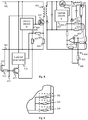
- Fig. 4 is a simplified circuit diagram that illustrates certain parts of a driver device used here as an example.
- the driver device of fig. 4 comprises a power input and some rectifying and filtering portions, but these are not shown in fig. 4 ; it is assumed that a relatively stable DC voltage appears between the voltage rails 401 and 402.
- the primary switched-mode converter stage is of the flyback type and comprises a transformer 403 and a switch 404. During a period when the switch 404 is conductive a current flows through the primary coil of the transformer 403, storing energy into its magnetic field. The current is measured with the help of a current sensing resistor network consisting of resistors 405, 406, and 407.
- the potential of a measurement point 408 constitutes an indicator of the current through the primary coil, and is sensed by the switch driver IC 409 that is responsible for producing the switching pulses for the switch 404.
- the network including resistors 405, 406, and 407, as well as the current sensing parts of the switch driver IC 409 are parts of a current feedback arrangement of the primary switched-mode converter stage in fig. 4 .
- the severable current path 107 has an effect on a gain of the current feedback arrangement of the primary switched-mode converter stage in fig. 4 .
- the mechanism and operation of this effect is described in the following.
- the current feedback arrangement comprises, in addition to the parts described above, a current generator 410 configured to change the potential of the measurement point 408: assuming that the current feedback input of the switch driver IC 409 has a high impedance and thus sinks only negligible current, a (positive) current generated by the current generator 410 will flow through the resistor network 405, 406, 407 to the lower voltage rail 402, tending to increase the potential of the measurement point 408. Further assuming that the switch driver IC 409 is configured to end an ongoing switching pulse when the sensed current reaches an upper limit, the current coming from the current generator 410 will cause this to happen earlier than if the current generator 410 was not generating any current: the current coming from the current generator increases the gain of the current feedback arrangement.
- the overall effect of the current generator 410 generating a current is to decrease that rate. Less energy is then available for the secondary switched-mode converter, which causes a corresponding decrease in output voltage and/or current.
- the driver device comprises an electrically controllable switch 411, placed so that depending on its conductivity it either enables or disables biasing the current generator 410 into operation.
- a necessary biasing connection from the current generator 410 to the local ground potential at rail 402 goes through the electrically controllable switch 411.
- the severable current path 107 constitutes a link between a control potential (which here is the local ground potential) and a control input (base) of the switch 411. If the switch 411 is an NPN transistor as in fig. 4 , and if the control potential is the local ground potential, as long as the current path 107 remains intact the switch 411 is non-conductive and the current generator 410 is inoperative, i.e. does not generate any current.
- the switch 411 receives a sufficient control signal into its control input in synchronism with the switching pulses of the switch 404, making the switch 411 conductive.
- the current generator 410 generates a current during each conduction period of the switch 404.
- the secondary switched-mode converter stage of the driver device in fig. 4 is of the buck type and comprises a switch 412 and a series inductor 413.
- a freewheeling current loop of the buck-type switched-mode converter goes through the load (LEDs) coupled across the LED current output 104, the current-sensing resistor 414, and the freewheeling diode 415.
- the current feedback arrangement of the secondary switched-mode converter stage comprises the current-sensing resistor 414 and a connection through resistor 416 to the current feedback input of the secondary-side switch control IC 417, as well as the current sensing parts of said switch control IC 417.
- the current feedback arrangement of the secondary switched-mode converter stage comprises a voltage generator configured to change the potential of the measurement point 418 the potential of which constitutes an indicator of the momentary output current of the driver device.
- a central part of the voltage generator is the comparator 419.
- the potential at the inverting input of the comparator 419 is a scaled sample of the potential of the upper node of the LED current output 104.
- resistor 421 there is also a connection from the non-inverting input of the comparator 419 to the local ground potential of the secondary switched-mode converter stage through resistor 421 and the severable current path 108.
- the connection from the non-inverting input of the comparator 419 to the local ground potential of the secondary switched-mode converter stage ensures that the output of the comparator 419 remains low. If the severable current path 108 is cut by removing the corresponding delineated portion of circuit board, the potential of the non-inverting input of the comparator 419 begins to follow the potential of the lower node of the LED current output 104. An increasing output current makes this potential higher.
- the output of the comparator 419 goes high, increasing the potential of the measurement point 418 and making the switch driver IC 417 believe that the output current is higher than it actually is.
- the electric conductivity of the severable current path 108 has an effect on the rate at which the voltage generator is capable of changing the potential of the measurement point 418, so ultimately the electric conductivity of said current path has an effect on the gain of the current feedback arrangement of the secondary switched-mode converter.
- a current generator like on the primary side of the driver device of fig. 4
- a voltage generator like on the secondary side
- an electrically controllable switch like on the primary side of the driver device of fig. 4
- a direct severable connection like on the secondary side
- both the primary and secondary side arrangements could be based on a current generator, or both of them could have a direct severable connection, etc.
- the severable current path and its effect on the output characteristics of the driver device are shown in association with both primary and secondary switched-mode converter stages in figs. 1 and 4 , they could be implemented in only one of said stages.
- a driver device with only one severable current path allows selecting only between two different sets of output characteristics
- a driver device with two severable current paths allows selecting among four sets of output characteristics.
- the manufacturer of driver devices may want to test all manufactured devices for correct operation before they are delivered to his customers. If it is meant that only the customer will decide the desired output characteristics, it is not possible to remove any delineated portions of circuit boards in the testing process of the manufacturer. Yet it would be advantageous if also those output characteristics could be tested that in practical use will only become operative after removing the corresponding delineated portion of circuit board.
- the driver device may comprise a test point for creating a condition where an external potential connected to such a test point without removing the corresponding delineated portion has the same effect on the operation of the driver device as the removal of the delineated portion without connecting said external potential to the test point.
- the primary switched-mode converter stage of the driver device in fig. 4 comprises a test point 422 that is located on the severable current path one resistor 423 away from the direct connection to the internal reference potential at the lower voltage rail 402.
- the secondary switched-mode converter stage comprises a test point 424 that is located on the severable current path one resistor 421 away from the direct connection to the internal reference potential of the secondary side, i.e. the local ground potential of the secondary switched-mode converter stage.
- the reason for the test point being at least one resistor away from any direct connection to an internal reference potential is that when, during testing, an external potential is connected to the test point, it does not change significantly the internal reference potential and thus does not cause confusion in the normal operation of the driver device.
- the driver device may first operate without any external potential connected to test point 422.
- the connection to voltage rail 402 will maintain the switch 411 non-conductive, and the operation at the first set of desired output characteristics may be tested.
- an external (positive) potential can be connected to test point 422.
- the external potential must be sufficiently high to make the switch 411 conductive, which is the same as would happen if the severable current path 107 was cut by removing the corresponding delineated portion of circuit board.
- the operation at the second set of desired output characteristics can be tested.
- test points are visible and accessible without opening the outer cover of the driver device, because this allows full testing of a completed driver device without opening its outer cover.
- this is not mandatory, since many of the tests of a manufacturer can be performed while the devices to be tested are still just circuit boards assembled with components, before they are enclosed in the outer covers.
- a method for setting the output characteristics of a driver device for semiconductor light sources comprises breaking off a delineated portion of a circuit board of the driver device along a weakened border of said delineated portion.
- a delineated portion carries a current path that is connected to at least some of the electronic components and conductive tracks on the rest of the circuit board.
- Said breaking off may comprise breaking off said delineated portion at an end of the circuit board that is visible and accessible outside a closed outer cover of the driver device.
- a delineated, removable portion of a circuit board may carry one or more electronic components in addition to just conductive tracks or pads, and/or the circuit board may comprise more than one delineated, removable portion carrying a part of the same current path. Examples of both these variations are shown schematically in fig. 5 .
- a current path comprises three resistors 501, 502, and 503, as well as the conductive tracks that are needed to connect the three resistors in parallel.
- Each resistor is attached to and supported by a delineated, removable portion of circuit board of its own. Removing any of the delineated, removable portions will cause a corresponding change in the total resistance of the current path, which then will have a corresponding effect on the operation of the driver device of which the current path is a part.
- Another class of variations involves placing the severable current path into some other part of the driver device than a current feedback arrangement.
- there may be resistors and/or capacitors in many places in a driver device, including but not being limited to current paths where so-called external resistors or capacitors (called external because they are not within the IC) set the operating frequency of a driver IC.
- the inductive components of the driver device may comprise parallel and/or serial options, of which only the desired ones are selected into use by cutting the current paths to the others through the removal of the corresponding delineated portions of circuit board.
Landscapes
- Dc-Dc Converters (AREA)
Abstract
Description
- The invention relates to setting the output characteristics of a driver device for semiconductor light sources, such as LEDs. In particular the invention relates to making such setting easy and straightforward at the stage of assembling a luminaire or otherwise finalising the combination of the various components that constitute the luminaire.
- Luminaires that employ semiconductor light sources such as LEDs need a driver device that feeds the available electric power to the LEDs at suitable voltage and current levels. Typically the raw electric power is AC mains at for example 230 V and 50 Hz. The output voltage of the driver device may be fixed DC at for example 12 V or 24 V, or it may be allowed to vary within a certain range so that it will meet the sum of forward threshold voltages of the LEDs connected in series across the output. Also the output current may be fixed at a suitable value, such as e.g. 350 mA, 700 mA, or 1050 mA, or it may be controllable to allow dimming the LEDs. A typical driver device comprises circuit elements such as rectifiers, filters, and one or more switched-mode converters to accomplish its task.
- On one hand a driver device should be as simple as possible to keep the manufacturing costs under control. On the other hand the manufacturer of LED luminaires wants to produce luminaires with different designs, different number and type of LEDs, and/or different amounts of produced light. Trying to fulfil all needs may lead to a relatively complicated matrix of decisions, where the luminaire manufacturer must either acquire complicated (and expensive) controllable drivers or stock a considerable variety of constant output drivers, trying to constantly meet the rapidly varying needs of his manufacturing lines.
- A compromise with some important advantages involves the use of drivers with settable output characteristics. According to a common approach such a driver device exhibits a two-pole connector, to which the luminaire manufacturer can attach a resistor of selected magnitude. The resistor becomes a part of the current feedback circuit of the driver device, with the effect that the output current will be set at a corresponding fixed value or range. A so-called Iset resistor of this kind may set the fixed output current level of a constant current driver, or it may set the upper limit of the output current range of a controllable driver. In some other cases the selected resistance of the externally connected resistor may set the output voltage, PWM frequency, or other output characteristic of the driver device.
- The disadvantages of the Iset resistor approach involve the need to stock and keep in order the various resistors, as well as the necessity of a relatively accurate assembling step in which a resistor is attached to the connector.
- It is an objective of the present invention to provide a driver device and a method for setting the output characteristics of a driver device in a way that allows streamlining the manufacturing processes of luminaires. Another objective of the present invention is to present a driver device with settable output characteristics that is cheap and easy to manufacture. Yet another objective of the present invention is to present such a driver device that can be easily tested for correct operation of all possible output characteristics at or after its manufacturing. A further objective of the invention is to present a driver device the output characteristics of which can be set accurately and with little variation between individual manufactured units.
- The objectives of the invention are achieved by making a circuit board of the driver device comprise one or more portions that can be easily snapped or cut off, so that removing those components and/or conductive track portions from the driver circuit that appeared on the removed portions of the circuit board has a desired effect on output characteristics.
- According to an aspect of the invention there is provided a driver device for semiconductor light sources. The driver device comprises a circuit board and electronic components and conductive tracks attached to and supported by said circuit board. The circuit board comprises a delineated portion through which goes at least one current path consisting of some of said conductive tracks and electronic components, the electric conductivity of said current path having an effect on output characteristics of said driver device. The structural strength of the circuit board is weakened at the border of said delineated portion for allowing controllable removal of said delineated portion without damaging the rest of the circuit board.
- According to another aspect of the invention there is provided a method for setting the output characteristics of a driver for semiconductor light sources. The method comprises breaking off a delineated portion of a circuit board of the driver device along a weakened border of said delineated portion, said delineated portion carrying a current path that is connected to at least some of the electronic components and conductive tracks on the rest of the circuit board.
- The invention is related to driving semiconductor light sources, such as LEDs, OLEDs, laser diodes, or the like. For simplicity the word LEDs is often used while the meaning is not to limit the discussion to just LEDs in a narrow sense but to semiconductor light sources in general.
- The exemplifying embodiments of the invention presented in this patent application are not to be interpreted to pose limitations to the applicability of the appended claims. The verb "to comprise" and its derivatives are used in this patent application as an open limitation that does not exclude the existence of features that are not recited. The features described hereinafter are mutually freely combinable unless explicitly stated otherwise.
- The novel features which are considered as characteristic of the invention are set forth in particular in the appended claims. The invention itself, however, both as to its construction and its method of operation, together with additional objects and advantages thereof, will be best understood from the following detailed description of specific embodiments when read in connection with the accompanying drawings.
-
- Figure 1
- illustrates a driver device for semiconductor light sources,
- figure 2
- illustrates a portion of a circuit board,
- figure 3
- illustrates a driver device with linear form factor,
- figure 4
- illustrates a circuit diagram of a driver device, and
- figure 5
- illustrates a portion of a circuit board.
-
Fig. 1 illustrates schematically adriver device 101 forsemiconductor light sources 102, which are illustrated in the form of LEDs. The driver device comprises apower input 103 and a LEDcurrent output 104. Of these thepower input 103 is typically meant to be coupled to AC mains. One or more switched-mode converter stages are provided for converting the energy drawn by thepower input 103 into a voltage and current that can be provided at the LEDcurrent output 104 to make thesemiconductor light sources 102 shine at a desired brightness. Thedriver device 101 comprises a primary switched-mode converter stage 105 and a secondary switched-mode converter stage 106 coupled in series between thepower input 103 and the LEDcurrent output 104. The primary switched-mode converter stage 105 is configured to perform PFC (power factor correction) and to produce a so-called internal bus voltage Vbus, which constitutes the input voltage to the secondary switched-mode converter stage 106. The secondary switched-mode converter stage 106 is configured to draw a current Ibus and to produce the output voltage Vout, which feeds an output current lout through thesemiconductor light sources 102. Such a two-stage structure of a driver device, as well as the tasks and operating principles of the two switched-mode converter stages, are as such well known to the person skilled in the art and they do not need to be discussed further. - By far the most common way of building an electronic device is to provide a circuit board with conductive tracks formed on its surface, and to solder or otherwise attach suitable electronic components to connection pads that form part of said conductive tracks. The primary and secondary switched-mode converter stages of
fig. 1 may be built on their own circuit boards, or they may be built at least partly on a common circuit board.Fig. 2 illustrates schematically a corner of acircuit board 201, withelectronic components 202 and 203 as well asconductive tracks circuit board 201 comprises also adelineated portion 207, through which goes at least one current path that consists of some of the conductive tracks and electronic components. Infig. 2 theelectronic components 202 and 203 as well as theconductive track 206 are parts of such a current path. The hatched pattern appears infig. 2 only to graphically demonstrate thedelineated portion 207, and it does not need to appear in any tangible form on the actual circuit board. - The structural strength of the circuit board is deliberately weakened at the border of the delineated
portion 207. Infig. 2 the weakening is accomplished by making perforated lines appear in the circuit board material along the border of the delineatedportion 207. The weakening would allow controllable removal of the delineatedportion 207 without damaging the rest of the circuit board. The delineatedportion 207 could be snapped off simply by bending it along the perforated lines, or a pair of cutoff pliers could be used to cut the delineatedportion 207 out. Removing the delineatedportion 207 would cut the current path that consists of theelectronic components 202 and 203 and theconductive track 206. Other ways of weakening the structural strength of the circuit board at the border of the delineatedportion 207 can be used: for example, at least some of the following (or any combination of any of the following) may appear along the border of the delineated portion: openings, perforated lines, and grooves. If the circuit board material is susceptible to local structural weakening through localized thermal treatment, like momentarily bringing a very hot and sharp object into contact with a selected point or line on the circuit board, such treatment can be used for causing the desired structural weakening. Yet another possibility is to allow a tightly focused beam of electromagnetic radiation, fluid, or fine particles to interact with the circuit board material, causing local structural weakening. - Comparing to
fig. 1 it can be assumed that said current path is part of the primary switched-mode converter stage 105, or part of the secondary switched-mode converter stage 106. The first alternative is illustrated schematically as the severablecurrent path 107, and the second alternative is illustrated schematically as the severablecurrent path 108. Yet another possibility is that the circuit board on which thedriver device 101 is built comprises two delineated portions of the kind described above (or a first circuit board on which the primary switched-mode converter stage 105 is built comprises one delineated portion and a second circuit board on which the secondary switched-mode converter stage 106 is built comprises another delineated portion), so that the current path going through one of the delineated portions is part of the primary switched-mode converter stage 105 and the current path going through the other of the delineated portions is part of the secondary switched-mode converter stage 106. - The idea is then that the electric conductivity of the current path has an effect on the output characteristics of the driver device: controllably removing the delineated portion of the circuit board causes a change in the electric conductivity of the current path, which in turn causes a change in the output characteristics. If the current path is part of the primary switched-
mode converter stage 105, likecurrent path 107 infig. 1 , a change in its electric conductivity may have an effect on the internal bus voltage Vbus or the current Ibus, which may in turn affect the operation of the secondary switched-mode converter stage 106. Thus the effect on the output characteristics of the driver device is somewhat indirect. A more direct effect may result if the current path is part of the secondary switched-mode converter stage 106, likecurrent path 108 infig. 1 . More detailed examples of how the electric conductivity of a current path may affect the output characteristics of the driver device are given later in this text. Yet another possibility is that the current path in question is part of a feedback arrangement through which the secondary switched-mode converter stage 106 provides feedback to the primary switched-mode converter stage 105. In such a case the current path in question may even be said to be part of both the primary and secondary switched-mode converter stages. - A driver device may comprise a closed outer cover that encloses a majority portion of the circuit board. It is advantageous if the delineated portion of the circuit board is visible and accessible outside the outer cover of the driver device, because this will facilitate making the desired change in the output characteristics of the driver device without opening its outer cover. At the time of writing this description it is common that driver devices are categorized as "linear" or "compact" devices according to their form factor: a linear driver device inherits its form factor from known electronic ballasts of fluorescent tube luminaires, so that the driver device is eye-catchingly elongated in form, while the relative dimensions of a compact device resemble those of a cigarette box.
- The driver device in
fig. 3 is an example of one having the form factor of a linear driver device, but the following considerations are easily generalized to cover also compact-formed driver devices. The driver device is shown in a side view (upper part offig. 3 ) and a top view (lower part offig. 3 ). It comprises an elongated outer cover that consists of abase part 301 and atop part 302. Also thecircuit board 201 has an elongated form in order to fit inside the outer cover, which enclosed a majority portion of thecircuit board 201 but leaves both ends of thecircuit board 201 visible and accessible. There areconnectors - The driver device of
fig. 3 has one delineatedportion 207 of the kind described above located at one end of the circuit board, next to theconnector 303. The component(s) and/or conductive track(s) of the current path going through the delineatedportion 207 are not shown infig. 3 ; they may be for example on that side of thecircuit board 201 that is against the inner surface of thebase part 301. An elongated driver device of this kind could comprise two delineated portions of the kind described above, for example one at each end of the circuit board. In a compact-formed driver device there may be a visible and accessible portion of the circuit board only on one side of the device, so that e.g. all connectors are concentrated on that side. In such a case the delineated portion could also be located next to the connector. If there are two delineated portions, they could be located for example at both sides of the connector arrangement in order to easily distinguish between them. As such there is no imperative reason why a delineated portion should be just next to a connector or connector arrangement, but since both a connector and a delineated portion benefit from being visible and easily accessible, and since the outer cover of a driver device typically leaves a relatively small proportion of the circuit board visible and accessible, in many cases the side by side placement of the connector and the delineated portion works well as a solution. - Even if the delineated portion was not accessible without opening the outer cover of the driver device, it may be advantageous to make it visible for example by making an opening in the outer cover. Namely, in many cases it is advantageous if it can be easily checked later, which output characteristics have been selected for which driver devices. A simple visual check may then be enough to tell, in which driver devices the delineated portion of the circuit board is still present and in which it has been removed.
-
Fig. 4 is a simplified circuit diagram that illustrates certain parts of a driver device used here as an example. The driver device offig. 4 comprises a power input and some rectifying and filtering portions, but these are not shown infig. 4 ; it is assumed that a relatively stable DC voltage appears between the voltage rails 401 and 402. The primary switched-mode converter stage is of the flyback type and comprises atransformer 403 and aswitch 404. During a period when theswitch 404 is conductive a current flows through the primary coil of thetransformer 403, storing energy into its magnetic field. The current is measured with the help of a current sensing resistor network consisting ofresistors measurement point 408 constitutes an indicator of the current through the primary coil, and is sensed by theswitch driver IC 409 that is responsible for producing the switching pulses for theswitch 404. Thus thenetwork including resistors switch driver IC 409 are parts of a current feedback arrangement of the primary switched-mode converter stage infig. 4 . - The severable
current path 107, the electric conductivity of which should have an indirect effect on the output characteristics of the driver device through affecting the operation of the primary switched-mode converter stage, has an effect on a gain of the current feedback arrangement of the primary switched-mode converter stage infig. 4 . The mechanism and operation of this effect is described in the following. - The current feedback arrangement comprises, in addition to the parts described above, a
current generator 410 configured to change the potential of the measurement point 408: assuming that the current feedback input of theswitch driver IC 409 has a high impedance and thus sinks only negligible current, a (positive) current generated by thecurrent generator 410 will flow through theresistor network lower voltage rail 402, tending to increase the potential of themeasurement point 408. Further assuming that theswitch driver IC 409 is configured to end an ongoing switching pulse when the sensed current reaches an upper limit, the current coming from thecurrent generator 410 will cause this to happen earlier than if thecurrent generator 410 was not generating any current: the current coming from the current generator increases the gain of the current feedback arrangement. Since the rate at which energy is transferred over thetransformer 403 depends on the primary current, the overall effect of thecurrent generator 410 generating a current is to decrease that rate. Less energy is then available for the secondary switched-mode converter, which causes a corresponding decrease in output voltage and/or current. - The driver device comprises an electrically
controllable switch 411, placed so that depending on its conductivity it either enables or disables biasing thecurrent generator 410 into operation. In the embodiment offig. 4 a necessary biasing connection from thecurrent generator 410 to the local ground potential atrail 402 goes through the electricallycontrollable switch 411. The severablecurrent path 107 constitutes a link between a control potential (which here is the local ground potential) and a control input (base) of theswitch 411. If theswitch 411 is an NPN transistor as infig. 4 , and if the control potential is the local ground potential, as long as thecurrent path 107 remains intact theswitch 411 is non-conductive and thecurrent generator 410 is inoperative, i.e. does not generate any current. If thecurrent path 107 is severed, theswitch 411 receives a sufficient control signal into its control input in synchronism with the switching pulses of theswitch 404, making theswitch 411 conductive. Thus thecurrent generator 410 generates a current during each conduction period of theswitch 404. - The secondary switched-mode converter stage of the driver device in
fig. 4 is of the buck type and comprises a switch 412 and aseries inductor 413. A freewheeling current loop of the buck-type switched-mode converter goes through the load (LEDs) coupled across the LEDcurrent output 104, the current-sensingresistor 414, and the freewheeling diode 415. The current feedback arrangement of the secondary switched-mode converter stage comprises the current-sensingresistor 414 and a connection throughresistor 416 to the current feedback input of the secondary-sideswitch control IC 417, as well as the current sensing parts of saidswitch control IC 417. - Additionally the current feedback arrangement of the secondary switched-mode converter stage comprises a voltage generator configured to change the potential of the
measurement point 418 the potential of which constitutes an indicator of the momentary output current of the driver device. A central part of the voltage generator is thecomparator 419. The potential at the inverting input of thecomparator 419 is a scaled sample of the potential of the upper node of the LEDcurrent output 104. To the non-inverting input of thecomparator 419 there exists a connection from the lower node of the LEDcurrent output 104 throughresistor 420. However, there is also a connection from the non-inverting input of thecomparator 419 to the local ground potential of the secondary switched-mode converter stage through resistor 421 and the severablecurrent path 108. - As long as the severable
current path 108 remains intact, the connection from the non-inverting input of thecomparator 419 to the local ground potential of the secondary switched-mode converter stage ensures that the output of thecomparator 419 remains low. If the severablecurrent path 108 is cut by removing the corresponding delineated portion of circuit board, the potential of the non-inverting input of thecomparator 419 begins to follow the potential of the lower node of the LEDcurrent output 104. An increasing output current makes this potential higher. If it becomes higher than the scaled sample of the potential of the upper node of the LEDcurrent output 104, the output of thecomparator 419 goes high, increasing the potential of themeasurement point 418 and making theswitch driver IC 417 believe that the output current is higher than it actually is. Thus the electric conductivity of the severablecurrent path 108 has an effect on the rate at which the voltage generator is capable of changing the potential of themeasurement point 418, so ultimately the electric conductivity of said current path has an effect on the gain of the current feedback arrangement of the secondary switched-mode converter. - The use of a current generator (like on the primary side of the driver device of
fig. 4 ) or a voltage generator (like on the secondary side), and the use of an electrically controllable switch (like on the primary side of the driver device offig. 4 ) or a direct severable connection (like on the secondary side) are variations that can be mixed and rearranged in various ways: both the primary and secondary side arrangements could be based on a current generator, or both of them could have a direct severable connection, etc. Also it should be noted that even if the severable current path and its effect on the output characteristics of the driver device are shown in association with both primary and secondary switched-mode converter stages infigs. 1 and4 , they could be implemented in only one of said stages. Naturally a driver device with only one severable current path allows selecting only between two different sets of output characteristics, while a driver device with two severable current paths allows selecting among four sets of output characteristics. - The manufacturer of driver devices may want to test all manufactured devices for correct operation before they are delivered to his customers. If it is meant that only the customer will decide the desired output characteristics, it is not possible to remove any delineated portions of circuit boards in the testing process of the manufacturer. Yet it would be advantageous if also those output characteristics could be tested that in practical use will only become operative after removing the corresponding delineated portion of circuit board.
- For testing purposes the driver device may comprise a test point for creating a condition where an external potential connected to such a test point without removing the corresponding delineated portion has the same effect on the operation of the driver device as the removal of the delineated portion without connecting said external potential to the test point. In other words,
- external potential connected to test point without removing delineated portion, or
- removing delineated portion and not having external potential connected to test point
- The primary switched-mode converter stage of the driver device in
fig. 4 comprises atest point 422 that is located on the severable current path oneresistor 423 away from the direct connection to the internal reference potential at thelower voltage rail 402. Similarly the secondary switched-mode converter stage comprises atest point 424 that is located on the severable current path one resistor 421 away from the direct connection to the internal reference potential of the secondary side, i.e. the local ground potential of the secondary switched-mode converter stage. The reason for the test point being at least one resistor away from any direct connection to an internal reference potential is that when, during testing, an external potential is connected to the test point, it does not change significantly the internal reference potential and thus does not cause confusion in the normal operation of the driver device. - For example when the operation of the primary side needs to be tested by the manufacturer, the driver device may first operate without any external potential connected to test
point 422. The connection tovoltage rail 402 will maintain theswitch 411 non-conductive, and the operation at the first set of desired output characteristics may be tested. Then an external (positive) potential can be connected to testpoint 422. The external potential must be sufficiently high to make theswitch 411 conductive, which is the same as would happen if the severablecurrent path 107 was cut by removing the corresponding delineated portion of circuit board. Thus the operation at the second set of desired output characteristics can be tested. - Similarly concerning the secondary side of the driver device of
fig. 4 , not connecting any external potential to testpoint 424 allows testing the operation with the secondary-side delineated portion of circuit board intact. Connecting a suitable external potential to testpoint 424 has the same effect as removing said delineated portion of circuit board, because it allows the potential of the non-inverting input of thecomparator 419 become higher than that of the inverting input. - It is advantageous if also the test points are visible and accessible without opening the outer cover of the driver device, because this allows full testing of a completed driver device without opening its outer cover. However, this is not mandatory, since many of the tests of a manufacturer can be performed while the devices to be tested are still just circuit boards assembled with components, before they are enclosed in the outer covers.
- A method according to the invention for setting the output characteristics of a driver device for semiconductor light sources, comprises breaking off a delineated portion of a circuit board of the driver device along a weakened border of said delineated portion. Such a delineated portion carries a current path that is connected to at least some of the electronic components and conductive tracks on the rest of the circuit board. Said breaking off may comprise breaking off said delineated portion at an end of the circuit board that is visible and accessible outside a closed outer cover of the driver device.
- Changes and modifications can be made to the exemplary embodiments described above without departing from the scope of protection defined by the appended claims. For example, a delineated, removable portion of a circuit board may carry one or more electronic components in addition to just conductive tracks or pads, and/or the circuit board may comprise more than one delineated, removable portion carrying a part of the same current path. Examples of both these variations are shown schematically in
fig. 5 . A current path comprises threeresistors - Another class of variations involves placing the severable current path into some other part of the driver device than a current feedback arrangement. As an example, there may be resistors and/or capacitors in many places in a driver device, including but not being limited to current paths where so-called external resistors or capacitors (called external because they are not within the IC) set the operating frequency of a driver IC. Or the inductive components of the driver device may comprise parallel and/or serial options, of which only the desired ones are selected into use by cutting the current paths to the others through the removal of the corresponding delineated portions of circuit board.
Claims (15)
- Driver device for semiconductor light sources, comprising:- a circuit board,- electronic components and conductive tracks attached to and supported by said circuit board,characterized in that- the circuit board comprises a delineated portion through which goes at least one current path consisting of some of said conductive tracks and electronic components, the electric conductivity of said current path having an effect on output characteristics of said driver device,- the structural strength of the circuit board is weakened at the border of said delineated portion for allowing controllable removal of said delineated portion without damaging the rest of the circuit board.
- A driver device according to claim 1, wherein the driver device comprises a closed outer cover enclosing a majority portion of said circuit board, and the delineated portion is visible and accessible outside said outer cover.
- A driver device according to claim 1 or 2, wherein the circuit board has an elongated form and the delineated portion is located at one end of the circuit board.
- A driver device according to claim 3, wherein:- the driver device comprises an elongated outer cover that encloses a majority portion of said circuit board but leaves both ends of the circuit board visible and accessible, and- the driver device comprises two delineated portions of the kind defined in claim 1, one at each end of the circuit board.
- A driver device according to any of the previous claims, wherein at least some of the following appear along the border of said delineated portion: openings, perforated lines, grooves.
- A driver device according to any of the previous claims, wherein:- some of said electronic components constitute a switched-mode converter,- said switched-mode converter comprises a current feedback arrangement,- the electric conductivity of said current path has an effect on a gain of said current feedback arrangement.
- A driver device according to claim 6, wherein:- said current feedback arrangement comprises a current or voltage generator configured to change the potential of a measurement point of said current feedback arrangement, and- the electric conductivity of said current path has an effect on the rate at which said current or voltage generator is capable of changing the potential of said measurement point.
- A driver device according to any of the preceding claims, wherein:- the driver device comprises an electrically controllable switch, and- said current path constitutes a link between a control potential and a control input of said switch.
- A driver device according to any of the preceding claims, wherein:- the driver device comprises a test point for creating a condition where an external potential connected to said test point without removing said delineated portion has the same effect on the operation of the driver device as the removal of the delineated portion without connecting said external potential to said test point.
- A driver device according to claim 9, wherein:- said current path constitutes a connection to an internal reference potential of the driver device, and- said test point is on said current path at least one resistor away from any direct connection to said internal reference potential.
- A driver device according to any of the preceding claims, wherein:- the driver device comprises a power input and a LED current output, as well as a primary switched-mode converter stage and a secondary switched-mode converter stage coupled in series between said power input and said LED current output, and- said current path is part of said primary switched-mode converter stage.
- A driver device according to any of claims 1 to 10, wherein:- the driver device comprises a power input and a LED current output, as well as a primary switched-mode converter stage and a secondary switched-mode converter stage coupled in series between said power input and said LED current output, and- said current path is part of said secondary switched-mode converter stage.
- A driver device according to any of claims 1 to 10, wherein- the driver device comprises a power input and a LED current output, as well as a primary switched-mode converter stage and a secondary switched-mode converter stage coupled in series between said power input and said LED current output, and- the driver device comprises two delineated portions of the kind defined in claim 1, so that the current path going through one of the delineated portions is part of the primary switched-mode converter stage and the current path going through the other of the delineated portions is part of the secondary switched-mode converter stage.
- A method for setting the output characteristics of a driver device for semiconductor light sources, comprising:- breaking off a delineated portion of a circuit board of the driver device along a weakened border of said delineated portion, said delineated portion carrying a current path that is connected to at least some of the electronic components and conductive tracks on the rest of the circuit board.
- A method according to claim 14, wherein said breaking off comprises breaking off said delineated portion at an end of the circuit board that is visible and accessible outside a closed outer cover of the driver device.
Priority Applications (1)
| Application Number | Priority Date | Filing Date | Title |
|---|---|---|---|
| EP17180295.2A EP3426004A1 (en) | 2017-07-07 | 2017-07-07 | Driver for light source with selectable output current |
Applications Claiming Priority (1)
| Application Number | Priority Date | Filing Date | Title |
|---|---|---|---|
| EP17180295.2A EP3426004A1 (en) | 2017-07-07 | 2017-07-07 | Driver for light source with selectable output current |
Publications (1)
| Publication Number | Publication Date |
|---|---|
| EP3426004A1 true EP3426004A1 (en) | 2019-01-09 |
Family
ID=59298379
Family Applications (1)
| Application Number | Title | Priority Date | Filing Date |
|---|---|---|---|
| EP17180295.2A Withdrawn EP3426004A1 (en) | 2017-07-07 | 2017-07-07 | Driver for light source with selectable output current |
Country Status (1)
| Country | Link |
|---|---|
| EP (1) | EP3426004A1 (en) |
Citations (5)
| Publication number | Priority date | Publication date | Assignee | Title |
|---|---|---|---|---|
| US5886875A (en) * | 1996-01-02 | 1999-03-23 | Motorola, Inc. | Apparatus using a circuit board having a frangible portion apparatus |
| US20020130985A1 (en) * | 2001-01-16 | 2002-09-19 | Weindorf Paul F. L. | Flexible led backlighting circuit |
| US20100020527A1 (en) * | 2008-07-23 | 2010-01-28 | Fiermuga Robert F | Emergency egress lighting system |
| EP3043624A1 (en) * | 2015-01-09 | 2016-07-13 | Helvar Oy Ab | LED driver with standby mode, and method for utlizing standby mode in a LED driver |
| EP3079445A1 (en) * | 2015-04-07 | 2016-10-12 | Helvar Oy Ab | Method and arrangement for setting the output current of a led driver |
-
2017
- 2017-07-07 EP EP17180295.2A patent/EP3426004A1/en not_active Withdrawn
Patent Citations (5)
| Publication number | Priority date | Publication date | Assignee | Title |
|---|---|---|---|---|
| US5886875A (en) * | 1996-01-02 | 1999-03-23 | Motorola, Inc. | Apparatus using a circuit board having a frangible portion apparatus |
| US20020130985A1 (en) * | 2001-01-16 | 2002-09-19 | Weindorf Paul F. L. | Flexible led backlighting circuit |
| US20100020527A1 (en) * | 2008-07-23 | 2010-01-28 | Fiermuga Robert F | Emergency egress lighting system |
| EP3043624A1 (en) * | 2015-01-09 | 2016-07-13 | Helvar Oy Ab | LED driver with standby mode, and method for utlizing standby mode in a LED driver |
| EP3079445A1 (en) * | 2015-04-07 | 2016-10-12 | Helvar Oy Ab | Method and arrangement for setting the output current of a led driver |
Similar Documents
| Publication | Publication Date | Title |
|---|---|---|
| JP4657382B1 (en) | Power circuit | |
| US20140176017A1 (en) | Power supply system, ripple suppression circuit and associated method | |
| EP2793276A1 (en) | Led lamp, lighting device including led lamp, and method for controlling electric current of led lamp | |
| White et al. | An average current modulation method for single-stage LED drivers with high power factor and zero low-frequency current ripple | |
| US8933649B2 (en) | Power converter having a switch coupled between windings | |
| US20120268039A1 (en) | Switching power supply with power feedback to keep lamp's brightness constant | |
| Monk | Electronics cookbook: practical electronic recipes with Arduino and Raspberry Pi | |
| Waniek et al. | Topology identification of electronic mass-market equipment for estimation of lifetime reduction by HF disturbances above 2 kHz | |
| US8796950B2 (en) | Feedback circuit for non-isolated power converter | |
| KR101387022B1 (en) | Power supply circuit | |
| JP6263769B2 (en) | LED power supply device and LED lighting device | |
| JP2016073000A (en) | Power supply device | |
| EP3540931A1 (en) | Voltage converter | |
| KR101142089B1 (en) | Ac /dc converter for led lighting and led lighting apparatus using the same | |
| US9479081B2 (en) | System for supplying a load with a parallel resonance | |
| US12563653B2 (en) | Current-limiting circuit for LED power supply | |
| CN108667312B (en) | Electronic device | |
| RU2611577C2 (en) | Adjustable flyback converter or intermediate buck converter | |
| McClusky | High voltage resonant self-tracking current-fed converter | |
| JP2009093216A (en) | Power supply device and lighting fixture | |
| JP2020140993A (en) | Transformer power supply circuit | |
| JP2014054131A (en) | Capacitor circuit, dc-dc converter circuit, and dc power-supply device | |
| EP3373018A1 (en) | Method and circuit for measuring current in a led driver | |
| Evnert | Design of future low-energy LED replacement for fluorescent tubes | |
| Heidinger | Long Life Single Stage PFC/SLC Converter driving LEDs |
Legal Events
| Date | Code | Title | Description |
|---|---|---|---|
| PUAI | Public reference made under article 153(3) epc to a published international application that has entered the european phase |
Free format text: ORIGINAL CODE: 0009012 |
|
| STAA | Information on the status of an ep patent application or granted ep patent |
Free format text: STATUS: THE APPLICATION HAS BEEN PUBLISHED |
|
| AK | Designated contracting states |
Kind code of ref document: A1 Designated state(s): AL AT BE BG CH CY CZ DE DK EE ES FI FR GB GR HR HU IE IS IT LI LT LU LV MC MK MT NL NO PL PT RO RS SE SI SK SM TR |
|
| AX | Request for extension of the european patent |
Extension state: BA ME |
|
| STAA | Information on the status of an ep patent application or granted ep patent |
Free format text: STATUS: REQUEST FOR EXAMINATION WAS MADE |
|
| 17P | Request for examination filed |
Effective date: 20190709 |
|
| RBV | Designated contracting states (corrected) |
Designated state(s): AL AT BE BG CH CY CZ DE DK EE ES FI FR GB GR HR HU IE IS IT LI LT LU LV MC MK MT NL NO PL PT RO RS SE SI SK SM TR |
|
| STAA | Information on the status of an ep patent application or granted ep patent |
Free format text: STATUS: EXAMINATION IS IN PROGRESS |
|
| 17Q | First examination report despatched |
Effective date: 20191001 |
|
| GRAP | Despatch of communication of intention to grant a patent |
Free format text: ORIGINAL CODE: EPIDOSNIGR1 |
|
| STAA | Information on the status of an ep patent application or granted ep patent |
Free format text: STATUS: GRANT OF PATENT IS INTENDED |
|
| RIC1 | Information provided on ipc code assigned before grant |
Ipc: H05B 45/37 20200101AFI20200528BHEP |
|
| INTG | Intention to grant announced |
Effective date: 20200626 |
|
| GRAS | Grant fee paid |
Free format text: ORIGINAL CODE: EPIDOSNIGR3 |
|
| STAA | Information on the status of an ep patent application or granted ep patent |
Free format text: STATUS: THE APPLICATION IS DEEMED TO BE WITHDRAWN |
|
| 18D | Application deemed to be withdrawn |
Effective date: 20210202 |