EP3425668A1 - Electrostatic discharge protection device - Google Patents
Electrostatic discharge protection device Download PDFInfo
- Publication number
- EP3425668A1 EP3425668A1 EP17180059.2A EP17180059A EP3425668A1 EP 3425668 A1 EP3425668 A1 EP 3425668A1 EP 17180059 A EP17180059 A EP 17180059A EP 3425668 A1 EP3425668 A1 EP 3425668A1
- Authority
- EP
- European Patent Office
- Prior art keywords
- input terminal
- esd
- power device
- voltage
- output terminal
- Prior art date
- Legal status (The legal status is an assumption and is not a legal conclusion. Google has not performed a legal analysis and makes no representation as to the accuracy of the status listed.)
- Withdrawn
Links
Images


Classifications
-
- H—ELECTRICITY
- H10—SEMICONDUCTOR DEVICES; ELECTRIC SOLID-STATE DEVICES NOT OTHERWISE PROVIDED FOR
- H10D—INORGANIC ELECTRIC SEMICONDUCTOR DEVICES
- H10D89/00—Aspects of integrated devices not covered by groups H10D84/00 - H10D88/00
- H10D89/60—Integrated devices comprising arrangements for electrical or thermal protection, e.g. protection circuits against electrostatic discharge [ESD]
- H10D89/601—Integrated devices comprising arrangements for electrical or thermal protection, e.g. protection circuits against electrostatic discharge [ESD] for devices having insulated gate electrodes, e.g. for IGFETs or IGBTs
- H10D89/811—Integrated devices comprising arrangements for electrical or thermal protection, e.g. protection circuits against electrostatic discharge [ESD] for devices having insulated gate electrodes, e.g. for IGFETs or IGBTs using FETs as protective elements
- H10D89/817—FETs in a Darlington configuration
Definitions
- the present invention relates to an electrostatic discharge (ESD) protection device and to an integrated circuit including an electrostatic discharge protection device.
- ESD electrostatic discharge
- FIG. 1a illustrates an active voltage clamping circuit for protecting an extended drain MOSFET 1.
- Active voltage clamping involves using a trigger device 2 or circuitry to switch on the primary high voltage device 1 when its drain-source voltage V ds approaches its breakdown voltage limit. This is in contrast to commonly-used parallel protection (shown in Figure 1b ), in which a second device 3, connected in parallel to the primary high voltage device 1, limits the voltage on the primary high voltage device 1.
- the active voltage clamping topology provides the benefit of smaller overall area, and thus lower cost, when compared with the parallel protection topology. This is partly because, in the parallel protection topology, the parallel-connected second device 3 needs sufficient device area to be able to absorb the excess energy associated with the ESD event or over-voltage. In contrast, in the active voltage clamping topology, the trigger device 2 can have a much smaller structure, as it only needs to provide the charge on the gate of the high voltage power device 1, while the excess energy is absorbed in the primary high voltage device 1.
- the primary high voltage device is generally sufficiently large (robust) to absorb the excess energy associated with ESD or over-voltage events without increasing the device size.
- the active voltage clamp protection topology also ensures that the excess charge, resulting from an over voltage or ESD event, is handled by the power device 1 in its "on-state” as it is switched on during these situations.
- the power device 1 can handle more current in “on-state” compared to “off-state", thereby allowing a larger current (energy) density and a smaller device area for such protection in "on-state”.
- the trigger circuitry used for switching on the primary high voltage device in case of an over voltage or ESD event comprises a Zener diode 2 or a stack of Zener diodes, connected between the drain and gate of the primary high voltage device 1.
- Capacitors are often added to speed up switch-on on the primary high voltage device to improve the robustness of the ESD protection for fast ESD pulses.
- an electrostatic discharge (ESD) protection device comprising:
- the trigger device may be used to trigger switching on the power device in the event of an overvoltage.
- the trigger device In the event of an over-voltage exceeding the breakdown voltage of the trigger device, the trigger device becomes conducting between its input and output terminals, generating a voltage at the control terminal of the power device. The power device thereby becomes conducting before its breakdown voltage is reached. This may also help to reduce the area overhead of the power device as is it is not required to withstand high overvoltages in its off-state.
- Said second breakdown voltage of said trigger device may be correlated with the said breakdown voltage of said power device
- a problem with the active voltage clamping arrangement shown in Figure 1 a is that the respective breakdown voltages of both the Zener diode 2 and the high voltage transistor 1 show production spread, and are non-correlated as the devices are created using different process steps. This non-correlated production spread reduces the achievable operation voltage range of the high voltage device at the high end of the voltage range.
- the operation voltage of the power device may be increased.
- Said power device and said trigger device may be transistors.
- Said power device and said trigger device may comprise the same type of transistor.
- This feature may ensure that the breakdown voltages of the power device and trigger device are correlated.
- Said power device and said trigger device may formed by the same process steps.
- This feature may ensure that the breakdown voltages of the power device and trigger device are correlated.
- the power device and trigger device may have the same device structure.
- Said first input terminal of said power device and said second input terminal of said trigger device may each be associated with a drift region.
- This feature may be used to support the high voltage capability of the power device, and may also be used to scale the breakdown voltage of the trigger device relative to the breakdown voltage of the power device.
- Said drift region of said second input terminal may be shorter than said drift region of said first input terminal.
- This feature may be used to ensure that said second breakdown voltage of said trigger device is lower than said breakdown voltage of said power device.
- the electrostatic discharge (ESD) protection device may further comprise a diode connected between said first control terminal and said first output terminal.
- This diode for example a Zener diode, may be used for limiting a voltage between said first control terminal and said first output terminal.
- the electrostatic discharge (ESD) protection device may further comprise a resistance between said second output terminal and said first output terminal.
- This feature may be used to scale the voltage generated at the first input terminal when the trigger device conducts a current between the second input and output terminals.
- Said second control terminal may be connected to said second output terminal.
- This feature may be used to configure the trigger device for operation in its off-state.
- the power device may comprise a first field effect transistor, wherein said first control terminal, said first input terminal and said first output terminal comprise a first gate, a first drain and a first source respectively of said first field effect transistor; and said trigger device may comprise a second field effect transistor, wherein said second control terminal, said second input terminal and said second output terminal comprise a second gate, a second drain and a second source respectively of said second field effect transistor.
- both the power device and trigger device as field effect transistors enables both devices to be created using the same process. This in turn enables the breakdown voltage of the trigger device to be correlated to the breakdown voltage of the power device, enabling the power device to be operated at a voltage closer to its breakdown voltage.
- Each of said first field effect transistor and said second field effect transistor may have an extended drain.
- An extended drain topology may be used to improve the high voltage capability of the power device.
- the length of extended drain may be determined based on the required breakdown voltage, and may therefore be used to scale the breakdown voltage of the trigger device.
- Said extended drain of said first field effect transistor may be longer than said extended drain of said second field effect transistor.
- This feature may be used to provide a lower breakdown voltage for the second field effect transistor than for the first field effect transistor.
- Each of said power device and said trigger device may be a MOSFET.
- Each of said power device and said trigger device may be an LDMOS transistor.
- an integrated circuit comprising an electrostatic discharge (ESD) protection device as defined above.
- ESD electrostatic discharge
- an electrostatic discharge (ESD) protection device comprising:
- an electrostatic discharge (ESD) protection device comprising:
- FIG. 2 shows an ESD protection device according to an embodiment of the invention, in the form of an active voltage clamping circuit 10.
- the circuit 10 may be incorporated in an integrated circuit.
- the circuit 10 shown in Figure 2 includes a power device 20, in the form of an extended drain n-channel MOSFET 20.
- An extended drain topology may be used, for example, to provide a high voltage capability for the power device 20.
- the power device 20 comprises a first control terminal 22 in the form of gate 22, a first input terminal 24 in the form of drain 24, and a first output terminal 26 in the form of source 26.
- a voltage V gs applied between the gate 22 and source 26 is used to switch the device 20 between an on-state for conduction between the drain 24 and source 26, and an off-state for blocking conduction between the drain 24 and source 26.
- V ds between the drain 24 and source 26 greater than a breakdown voltage V bd of the power device 20 results in non-destructive conduction between the drain 24 and source 26.
- the MOSFET 20 may be used, for example, for switching power to another device connected to the source 26 or drain 24.
- the circuit 10 further includes a trigger device 30, in the form of an extended drain n-channel MOSFET 30.
- the trigger device 30 may be used to trigger the power device 20 to switch to its on-state in the event of an overvoltage at the drain 24 of the power device 20.
- An overvoltage is a voltage which approaches the breakdown voltage V bd of the power device 20 for off-state drain-source conduction.
- the trigger device 30 comprises a second control terminal 32 in the form of gate 32, a second input terminal 34 in the form of drain 34, and a second output terminal 36 in the form of source 36.
- the gate 32 and source 36 of the trigger device 30 are connected so that the applied voltage V gs ' between the gate 32 and source 36 is effectively zero, causing the trigger device 30 to remain in its off-state for blocking conduction between the drain 34 and source 36.
- V ds ' between the drain 34 and source 36 of the trigger device 30 greater than a breakdown voltage V bd ' of the trigger device 30 results in non-destructive conduction between the drain 34 and source 36.
- the second input terminal or drain 34 of the trigger device 30 is connected to the second input terminal or drain 24 of the power device 20.
- the second output terminal or source 36 of the trigger device 30 is connected via a diode 40 to the first control terminal or gate 22 of the power device 20.
- a resistor 42 and Zener diode 44 are connected in parallel between the gate 22 and source 26 of the power device 20.
- the resistor 42 limits current through the trigger device 30.
- the Zener diode 44 limits the voltage at the gate 22 of the power device 20.
- the trigger device 30 When a voltage greater than the breakdown voltage V bd ' of the trigger device 30 appears at the drain 34 of the trigger device 30 (and thus also at the drain 24 of the power device 20), the trigger device 30 enters non-destructive breakdown and a current is conducted between the drain 34 and source 36 of the trigger device 30.
- This breakdown current flows through resistor 42, generating a voltage between the gate 22 and source 26 of the power device 20, so that the power device 20 is switched to its on-state and conducts current between its drain 24 and source 26. Energy associated with the overvoltage is thereby dissipated by the power device 20.
- the breakdown voltage V bd ' of the trigger device 30 is lower than the breakdown voltage V bd of the power device 20.
- the trigger device 30 enters breakdown and switches on the power device 20, avoiding the power device 20 entering breakdown in its off-state. This helps to protect the power device 20 from damage due to over-voltage and other ESD events because the power device 20 can handle more current in its on-state than in its off-state.
- the trigger device 30 can be much smaller than the power device 20 as it only has to provide the charge on the gate 22 of the power device 20, while the excess energy is absorbed by the power device 20.
- the power device 20 is typically sufficiently large to absorb the energy associated with overvoltage and other ESD events without any increase in size.
- the breakdown voltages V bd and V bd ' of the power device 20 and trigger device 30 may be correlated because the power device 20 and trigger device 30 are created using the same process steps and are subject to similar production spread. This enables the power device 20 to be operated at a higher voltage compared with the arrangement shown in Figure 1a , as will be explained in the following.
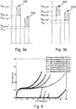
- FIG. 3a illustrates non-correlated breakdown voltages.
- the breakdown voltage V bd of the power device 20 (left-hand bar 120) has a minimum value V bd_min and a maximum value V bd_max due to production spread.
- the breakdown voltage V bd ' of the trigger device 30 (right-hand bar 130) also has a minimum value V bd_min ' and a maximum value V bd_max ' due to production spread.
- the breakdown voltage of the trigger device 30 must be specified so that its maximum value V bd_max ' is smaller than the minimum value V bd_min of the breakdown voltage of the power device 20.
- the maximum guaranteed operation voltage V op of the power device 20 must then be specified at a value smaller than the minimum breakdown voltage V bd_min ' of the trigger device 30. As can be seen from Figure 3a , this sets the guaranteed operation voltage V op of the power device 20 significantly lower than the minimum breakdown voltage V bd_min of the power device 20.
- Figure 3b illustrates correlated breakdown voltages, as implemented in the present disclosure. Now that the breakdown voltages of the power device 20 (left-hand bar 220) and trigger device 30 (right-hand bar 230) are correlated, the breakdown V bd ' of the trigger device 30 may be specified at a higher value than in the non-correlated case and its maximum value V bd_max ' may be greater than the minimum breakdown voltage V bd_min of the power device 20.
- the maximum value V bd_max ' of the breakdown voltage of the trigger device 30 must smaller than the maximum value V bd_max of the breakdown voltage of the power device 20, and the minimum value V bd_min ' of the breakdown voltage of the trigger device 30 must be smaller than the minimum value V bd_min of the breakdown voltage of the power device 20.
- the resulting maximum guaranteed operation voltage V op of the power device 20, specified at a value less than the minimum breakdown voltage V bd_min ' of the trigger device 30, is higher in the correlated case ( Figure 3b ) than in the non-correlated case ( Figure 3a ).
- a trigger device 30 with a breakdown voltage V bd ' correlated with the breakdown voltage V bd of the power device 20 allows the maximum operation voltage V op of the power device 20 to be increased so that it is closer to the breakdown voltage V bd of the power device 20.
- the extended drain topology of the MOSFETs 20, 30 included in the embodiment shown in Figure 2 provides a means for scaling the breakdown voltages, as the breakdown voltage of the MOSFET depends on the length of the extended drain structure.
- This is an experimentally proven result as illustrated by the test data shown in Figure 4 , which show drain-source voltage when applying a pulsed drain-source current for example MOSFETs having extended drains of different lengths.
- the four upper curves in Figure 4 show drain-source current vs drain-source voltage in the on-state.
- the four lower curves in Figure 4 show drain-source current vs drain-source voltage in the off-state.
- the length of the drift region of the drain increases from the left-most curve to the right-most curve.
- the breakdown voltage for drain-source conduction in the off-state is indicated by the sharp increase in current in the lower curves, and increases with increasing length of the extended drain or drift region.
- the trigger device 30 of the circuit 10 may be implemented by an extended drain device with a shorter extended drain length than that of the power device 20. This ensures a lower breakdown voltage for the trigger device 30 than for the power device 20. A high level of correlation between the breakdown voltages of the trigger device 30 and power device 20 is ensured as they are created with the same device structure and process steps, resulting in correlated production spread.
- Figure 5 illustrates the response of the circuit of Figure 2 to an applied drain-source voltage V ds .
- the curve (a) shows drain-source current I ds vs drain-source voltage V ds for the power device 20 in its off-state and indicates breakdown at a first drain-source breakdown voltage V bd , at which point the drain-source breakdown current begins to flow, increasing with increasing applied voltage.
- the curve (b) shows the corresponding drain-source current I ds ' vs drain-source voltage V ds ' for the trigger device 30 in its off-state and indicates breakdown at a second drain-source breakdown voltage V bd ' which is specified at a lower value than the breakdown voltage V bd of the power device 20.
- the gate-source voltage V gs of the power device 20 increases accordingly, as shown by curve (c) of Figure 5 .
- the increase in gate-source voltage V gs causes the power device 20 to be switched to its on-state, and the power device 20 starts to conduct a drain-source current I ds in its on-state, as indicated by curve (d) of Figure 5 .
- an overvoltage event results in the power device 20 being switched to its on-state (conducting state) before its drain-source breakdown voltage is reached.
- the power device 20 thereby dissipates the excess energy associated with the overvoltage event in its on-state, helping to avoid damage.
- FIGs 6a and 6b illustrate a drain extended metal oxide semiconductor transistor and an LDMOS (laterally-diffused metal oxide semiconductor) transistor respectively, each of which are suitable for use as both the power device and trigger device in the present invention.
- the extended drain transistor 300 shown in Figure 6a comprises a gate 302, drain 304, source 306, and an n- drain extension 305.
- the LDMOS transistor 400 with shallow-trench isolation (STI) shown in Figure 6b comprises a gate 402, drain 404 and source 406.
- An applied voltage is dropped across a drift region 405 between the external drain 404 and the internal channel 408 of the transistor 400.
- the breakdown voltage of the transistor increases with the length L drift of the drift region 405.
- the skilled person will appreciate that the invention is applicable to power/trigger devices having structures other than those described above.
- the breakdown voltages of the power device and trigger device are correlated, enabling the power device to be operated at a voltage higher than in the non-correlated case. Correlation of the respective breakdown voltages may be achieved by implementing the trigger device and power device using the same device structure, so that they are created using the same process steps, resulting in correlated production spread. Thus any power device requiring a trigger voltage to be switched to its on-state may be used.
- the power device 20 described above may be substituted by an IGBT, provided that the trigger device 30 is also substituted by an IGBT.
- the power/trigger devices described above may be substituted by other types of transistor, including other types of field effect transistors and bipolar transistors.
- any device having an extended drain or a drift region such as extended drain MOSFETs and laterally diffused MOS (LDMOS), provide a useful means for scaling the relative breakdown voltages of the power device and trigger device.
- LDMOS in which voltage is dropped along a drift region, a longer drift region is used to obtain a higher breakdown voltage of the device.
- the ESD protection device comprises a power device comprising a first control terminal, a first input terminal and a first output terminal, wherein a voltage at the first control terminal is controllable to switch the power device between an on-state for conducting a current between the first input terminal and the first output terminal, and an off-state for blocking a current between the first input terminal and the first output terminal, wherein the power device is configured for conduction between the first input terminal and the first output terminal, in the off-state, when an applied voltage between the first input terminal and the first output terminal exceeds a first breakdown voltage.
- the ESD device also comprises a trigger device comprising a second control terminal, a second input terminal and a second output terminal, wherein the trigger device is configured to operate in an off-state for blocking a current between the second input terminal and the second output terminal, wherein the trigger device is configured for conduction between the second input terminal and the second output terminal, in the off-state, when an applied voltage between the second input terminal and the second output terminal exceeds a second breakdown voltage.
- the second input terminal is connected to the first input terminal and the second output terminal is connected to the first control terminal.
- the second breakdown voltage of the trigger device is lower than the first breakdown voltage of the power device.
Landscapes
- Semiconductor Integrated Circuits (AREA)
- Metal-Oxide And Bipolar Metal-Oxide Semiconductor Integrated Circuits (AREA)
Abstract
An electrostatic discharge (ESD) protection device (10), and an integrated circuit comprising the same, are described. The ESD protection device (10) comprises a power device (20) comprising a first control terminal (22), a first input terminal (24) and a first output terminal (26), wherein a voltage at the first control terminal (22) is controllable to switch the power device (20) between an on-state for conducting a current between the first input terminal (24) and the first output terminal (26), and an off-state for blocking a current between the first input terminal (24) and the first output terminal (26), wherein the power device (20) is configured for conduction between the first input terminal (24) and the first output terminal (24), in the off-state, when an applied voltage between the first input terminal (24) and the first output terminal (26) exceeds a first breakdown voltage (Vbd). The ESD device (10) also comprises a trigger device (30) comprising a second control terminal (32), a second input terminal (34) and a second output terminal (36), wherein the trigger device (30) is configured to operate in an off-state for blocking a current between the second input terminal (34) and the second output terminal (36), wherein the trigger device (30) is configured for conduction between the second input terminal (34) and the second output terminal (36), in the off-state, when an applied voltage between the second input terminal (34) and the second output terminal (36) exceeds a second breakdown voltage (Vbd'). The second input terminal (34) is connected to the first input terminal (24). The second output terminal (36) is connected to the first control terminal (22). The power device (20) and the trigger device (30) may be transistors. The second breakdown voltage (Vbd') of the trigger device (30) is lower than the first breakdown voltage (Vbd) of the power device (20).
Description
- The present invention relates to an electrostatic discharge (ESD) protection device and to an integrated circuit including an electrostatic discharge protection device.
- Many high voltage devices embedded in integrated circuit (IC) processes use an extended drain topology to realize the high voltage capability of the device. Active voltage clamping is an efficient method for protecting a high voltage device embedded in an IC process against over-voltage events, especially electrostatic discharge (ESD) events.
Figure 1a illustrates an active voltage clamping circuit for protecting an extendeddrain MOSFET 1. Active voltage clamping involves using atrigger device 2 or circuitry to switch on the primaryhigh voltage device 1 when its drain-source voltage Vds approaches its breakdown voltage limit. This is in contrast to commonly-used parallel protection (shown inFigure 1b ), in which asecond device 3, connected in parallel to the primaryhigh voltage device 1, limits the voltage on the primaryhigh voltage device 1. - The active voltage clamping topology provides the benefit of smaller overall area, and thus lower cost, when compared with the parallel protection topology. This is partly because, in the parallel protection topology, the parallel-connected
second device 3 needs sufficient device area to be able to absorb the excess energy associated with the ESD event or over-voltage. In contrast, in the active voltage clamping topology, thetrigger device 2 can have a much smaller structure, as it only needs to provide the charge on the gate of the highvoltage power device 1, while the excess energy is absorbed in the primaryhigh voltage device 1. The primary high voltage device is generally sufficiently large (robust) to absorb the excess energy associated with ESD or over-voltage events without increasing the device size. - The active voltage clamp protection topology also ensures that the excess charge, resulting from an over voltage or ESD event, is handled by the
power device 1 in its "on-state" as it is switched on during these situations. Generally, thepower device 1 can handle more current in "on-state" compared to "off-state", thereby allowing a larger current (energy) density and a smaller device area for such protection in "on-state". - Typically, the trigger circuitry used for switching on the primary high voltage device in case of an over voltage or ESD event comprises a Zener
diode 2 or a stack of Zener diodes, connected between the drain and gate of the primaryhigh voltage device 1. Capacitors are often added to speed up switch-on on the primary high voltage device to improve the robustness of the ESD protection for fast ESD pulses. - Aspects of the invention are set out in the accompanying claims. Combinations of features from the dependent claims may be combined with features of the independent claims as appropriate and not merely as explicitly set out in the claims.
- According to an aspect of the invention, there is provided an electrostatic discharge (ESD) protection device, comprising:
- a power device comprising a first control terminal, a first input terminal and a first output terminal, wherein a voltage at said first control terminal is controllable to switch the power device between an on-state for conducting a current between said first input terminal and said first output terminal, and an off-state for blocking a current between said first input terminal and said first output terminal, wherein said power device is configured for conduction between said first input terminal and said first output terminal, in said off-state, when an applied voltage between said first input terminal and said first output terminal exceeds a first breakdown voltage; and
- a trigger device comprising a second control terminal, a second input terminal and a second output terminal, wherein said trigger device is configured to operate in an off-state for blocking a current between said second input terminal and said second output terminal, wherein said trigger device is configured for conduction between said second input terminal and said second output terminal, in said off-state, when an applied voltage between said second input terminal and said second output terminal exceeds a second breakdown voltage;
- wherein said second input terminal is connected to said first input terminal; and said second output terminal is connected to said first control terminal;
- wherein said second breakdown voltage of said trigger device is lower than said first breakdown voltage of said power device.
- By ensuring that the breakdown voltage of the trigger device is lower than the breakdown voltage of the power device, the trigger device may be used to trigger switching on the power device in the event of an overvoltage. In the event of an over-voltage exceeding the breakdown voltage of the trigger device, the trigger device becomes conducting between its input and output terminals, generating a voltage at the control terminal of the power device. The power device thereby becomes conducting before its breakdown voltage is reached. This may also help to reduce the area overhead of the power device as is it is not required to withstand high overvoltages in its off-state.
- Said second breakdown voltage of said trigger device may be correlated with the said breakdown voltage of said power device
- This enables the power device to be operated at a voltage closer to its breakdown voltage. A problem with the active voltage clamping arrangement shown in
Figure 1 a is that the respective breakdown voltages of both theZener diode 2 and thehigh voltage transistor 1 show production spread, and are non-correlated as the devices are created using different process steps. This non-correlated production spread reduces the achievable operation voltage range of the high voltage device at the high end of the voltage range. By using a trigger device having a breakdown voltage correlated with the breakdown voltage of the power device, the operation voltage of the power device may be increased. - Said power device and said trigger device may be transistors.
- Said power device and said trigger device may comprise the same type of transistor.
- This feature may ensure that the breakdown voltages of the power device and trigger device are correlated.
- Said power device and said trigger device may formed by the same process steps.
- This feature may ensure that the breakdown voltages of the power device and trigger device are correlated. By forming the power device and trigger device by the same process, the power device and trigger device may have the same device structure.
- Said first input terminal of said power device and said second input terminal of said trigger device may each be associated with a drift region.
- This feature may be used to support the high voltage capability of the power device, and may also be used to scale the breakdown voltage of the trigger device relative to the breakdown voltage of the power device.
- Said drift region of said second input terminal may be shorter than said drift region of said first input terminal.
- This feature may be used to ensure that said second breakdown voltage of said trigger device is lower than said breakdown voltage of said power device.
- The electrostatic discharge (ESD) protection device may further comprise a diode connected between said first control terminal and said first output terminal.
- This diode, for example a Zener diode, may be used for limiting a voltage between said first control terminal and said first output terminal.
- The electrostatic discharge (ESD) protection device may further comprise a resistance between said second output terminal and said first output terminal.
- This feature may be used to scale the voltage generated at the first input terminal when the trigger device conducts a current between the second input and output terminals.
- Said second control terminal may be connected to said second output terminal.
- This feature may be used to configure the trigger device for operation in its off-state.
- The power device may comprise a first field effect transistor, wherein said first control terminal, said first input terminal and said first output terminal comprise a first gate, a first drain and a first source respectively of said first field effect transistor; and said trigger device may comprise a second field effect transistor, wherein said second control terminal, said second input terminal and said second output terminal comprise a second gate, a second drain and a second source respectively of said second field effect transistor.
- Implementing both the power device and trigger device as field effect transistors enables both devices to be created using the same process. This in turn enables the breakdown voltage of the trigger device to be correlated to the breakdown voltage of the power device, enabling the power device to be operated at a voltage closer to its breakdown voltage.
- Each of said first field effect transistor and said second field effect transistor may have an extended drain.
- An extended drain topology may be used to improve the high voltage capability of the power device. In addition, the length of extended drain may be determined based on the required breakdown voltage, and may therefore be used to scale the breakdown voltage of the trigger device.
- Said extended drain of said first field effect transistor may be longer than said extended drain of said second field effect transistor.
- This feature may be used to provide a lower breakdown voltage for the second field effect transistor than for the first field effect transistor.
- Each of said power device and said trigger device may be a MOSFET.
- Each of said power device and said trigger device may be an LDMOS transistor.
- According to another aspect of the invention, there is provided plurality of electrostatic discharge (ESD) protection devices as defined above, wherein said second breakdown voltages of said trigger devices of said electrostatic discharge (ESD) devices are correlated with said first breakdown voltages of said corresponding power devices of said respective electrostatic discharge (ESD) devices.
- According to another aspect of the invention, there is provided an integrated circuit comprising an electrostatic discharge (ESD) protection device as defined above.
- According to another aspect of the invention, there is provided an electrostatic discharge (ESD) protection device, comprising:
- a first field effect transistor comprising a first gate, a first drain and a first source, wherein a voltage at said first gate is controllable to switch the first field effect transistor between an on-state for conducting a current between said first gate and said first source, and an off-state for blocking a current between said first gate and said first source, wherein said first field effect transistor is configured for conduction between said first gate and said first source, in said off-state, when an applied voltage between said first gate and said first source exceeds a first breakdown voltage; and
- a second field effect transistor comprising a second gate, a second drain and a second source, wherein said second field effect transistor is configured to operate in an off-state for blocking a current between said second drain and said second source, wherein said trig second field effect transistor is configured for conduction between said second gate and said second source, in said off-state, when an applied voltage between said second gate and said second source exceeds a second breakdown voltage;
- wherein said second drain is connected to said first drain; and said second source is connected to said first gate;
- wherein said second breakdown voltage is lower than said first breakdown voltage.
- According to another aspect of the invention, there is provided a method for manufacturing an electrostatic discharge (ESD) protection device, comprising:
- forming a power device comprising a first control terminal, a first input terminal and a first output terminal, wherein a voltage at said first control terminal is controllable to switch the power device between an on-state for conducting a current between said first input terminal and said first output terminal, and an off-state for blocking a current between said first input terminal and said first output terminal, wherein said power device is configured for conduction between said first input terminal and said first output terminal, in said off-state, when an applied voltage between said first input terminal and said first output terminal exceeds a first breakdown voltage; and
- forming a trigger device comprising a second control terminal, a second input terminal and a second output terminal, wherein said trigger device is configured to operate in an off-state for blocking a current between said second input terminal and said second output terminal, wherein said trigger device is configured for conduction between said second input terminal and said second output terminal, in said off-state, when an applied voltage between said second input terminal and said second output terminal exceeds a second breakdown voltage;
- forming a connection between said second input terminal and said first input terminal; and forming a connection between said second output terminal and said first control terminal;
- wherein said second breakdown voltage of said trigger device is lower than said first breakdown voltage of said power device;
- wherein the same process is used for forming each of said power device and said trigger device.
- Embodiments of the present invention will be described, by way of example only, with reference to the accompanying drawings in which like reference signs relate to like elements and in which:
-
Figure 1 a shows an active voltage clamping circuit for ESD protection as known in the prior art; -
Figure 1b shows a parallel protection circuit for ESD protection as known in the prior art; -
Figure 2 shows an ESD protection circuit according to an embodiment of the invention; -
Figure 3 illustrates an effect of (a) non-correlated and (b) correlated breakdown voltages of the power device and trigger device of an active voltage clamping circuit; -
Figure 4 illustrates the current-voltage relationship for an extended drain MOSFET; -
Figure 5 illustrates the response of the trigger device and power device in the circuit ofFigure 2 to applied drain-source voltage; and -
Figures 6a and 6b illustrate an extended drain transistor and a LDMOS transistor respectively. -
Figure 2 shows an ESD protection device according to an embodiment of the invention, in the form of an activevoltage clamping circuit 10. Thecircuit 10 may be incorporated in an integrated circuit. - The
circuit 10 shown inFigure 2 includes apower device 20, in the form of an extended drain n-channel MOSFET 20. An extended drain topology may be used, for example, to provide a high voltage capability for thepower device 20. Thepower device 20 comprises afirst control terminal 22 in the form ofgate 22, afirst input terminal 24 in the form ofdrain 24, and afirst output terminal 26 in the form ofsource 26. A voltage Vgs applied between thegate 22 andsource 26 is used to switch thedevice 20 between an on-state for conduction between thedrain 24 andsource 26, and an off-state for blocking conduction between thedrain 24 andsource 26. In the off-state, application of voltage Vds between thedrain 24 andsource 26 greater than a breakdown voltage Vbd of thepower device 20 results in non-destructive conduction between thedrain 24 andsource 26. TheMOSFET 20 may be used, for example, for switching power to another device connected to thesource 26 ordrain 24. - The
circuit 10 further includes atrigger device 30, in the form of an extended drain n-channel MOSFET 30. Thetrigger device 30 may be used to trigger thepower device 20 to switch to its on-state in the event of an overvoltage at thedrain 24 of thepower device 20. An overvoltage is a voltage which approaches the breakdown voltage Vbd of thepower device 20 for off-state drain-source conduction. - The
trigger device 30 comprises asecond control terminal 32 in the form ofgate 32, asecond input terminal 34 in the form ofdrain 34, and asecond output terminal 36 in the form ofsource 36. Thegate 32 andsource 36 of thetrigger device 30 are connected so that the applied voltage Vgs' between thegate 32 andsource 36 is effectively zero, causing thetrigger device 30 to remain in its off-state for blocking conduction between thedrain 34 andsource 36. In the off-state, application of voltage Vds' between thedrain 34 andsource 36 of thetrigger device 30 greater than a breakdown voltage Vbd' of thetrigger device 30 results in non-destructive conduction between thedrain 34 andsource 36. - The second input terminal or drain 34 of the
trigger device 30 is connected to the second input terminal or drain 24 of thepower device 20. The second output terminal orsource 36 of thetrigger device 30 is connected via adiode 40 to the first control terminal orgate 22 of thepower device 20. Aresistor 42 andZener diode 44 are connected in parallel between thegate 22 andsource 26 of thepower device 20. Theresistor 42 limits current through thetrigger device 30. TheZener diode 44 limits the voltage at thegate 22 of thepower device 20. - When a voltage greater than the breakdown voltage Vbd' of the
trigger device 30 appears at thedrain 34 of the trigger device 30 (and thus also at thedrain 24 of the power device 20), thetrigger device 30 enters non-destructive breakdown and a current is conducted between thedrain 34 andsource 36 of thetrigger device 30. This breakdown current flows throughresistor 42, generating a voltage between thegate 22 andsource 26 of thepower device 20, so that thepower device 20 is switched to its on-state and conducts current between itsdrain 24 andsource 26. Energy associated with the overvoltage is thereby dissipated by thepower device 20. - The breakdown voltage Vbd' of the
trigger device 30 is lower than the breakdown voltage Vbd of thepower device 20. Thus in the event of an overvoltage at thedrain 24 of thepower device 20, thetrigger device 30 enters breakdown and switches on thepower device 20, avoiding thepower device 20 entering breakdown in its off-state. This helps to protect thepower device 20 from damage due to over-voltage and other ESD events because thepower device 20 can handle more current in its on-state than in its off-state. - The
trigger device 30 can be much smaller than thepower device 20 as it only has to provide the charge on thegate 22 of thepower device 20, while the excess energy is absorbed by thepower device 20. Thepower device 20 is typically sufficiently large to absorb the energy associated with overvoltage and other ESD events without any increase in size. - By using matched devices (i.e the same type of device) for the
power device 20 and trigger device 30 (for example, both are extended drain MOSFETs in the embodiment shown inFigure 2 ), the breakdown voltages Vbd and Vbd' of thepower device 20 andtrigger device 30 may be correlated because thepower device 20 andtrigger device 30 are created using the same process steps and are subject to similar production spread. This enables thepower device 20 to be operated at a higher voltage compared with the arrangement shown inFigure 1a , as will be explained in the following. - In the arrangement shown in
Figure 1a , the breakdown voltages of both theZener diode 2 and thepower transistor 1 show production spread, but these breakdown voltages are non-correlated as theZener diode 2 and thepower transistor 1 are created using different process steps. This non-correlated production spread reduces the achievable maximum operation voltage of thepower transistor 1. This is explained with reference toFigure 3 , which illustrates the effect of correlated and non-correlated breakdown voltages of the power device and trigger device. -
Figure 3a illustrates non-correlated breakdown voltages. The breakdown voltage Vbd of the power device 20 (left-hand bar 120) has a minimum value Vbd_min and a maximum value Vbd_max due to production spread. The breakdown voltage Vbd' of the trigger device 30 (right-hand bar 130) also has a minimum value Vbd_min' and a maximum value Vbd_max' due to production spread. In order to ensure that thetrigger device 30 has a lower breakdown voltage than thepower device 20, the breakdown voltage of thetrigger device 30 must be specified so that its maximum value Vbd_max' is smaller than the minimum value Vbd_min of the breakdown voltage of thepower device 20. The maximum guaranteed operation voltage Vop of thepower device 20 must then be specified at a value smaller than the minimum breakdown voltage Vbd_min' of thetrigger device 30. As can be seen fromFigure 3a , this sets the guaranteed operation voltage Vop of thepower device 20 significantly lower than the minimum breakdown voltage Vbd_min of thepower device 20. -
Figure 3b illustrates correlated breakdown voltages, as implemented in the present disclosure. Now that the breakdown voltages of the power device 20 (left-hand bar 220) and trigger device 30 (right-hand bar 230) are correlated, the breakdown Vbd' of thetrigger device 30 may be specified at a higher value than in the non-correlated case and its maximum value Vbd_max' may be greater than the minimum breakdown voltage Vbd_min of thepower device 20. Of course, the maximum value Vbd_max' of the breakdown voltage of thetrigger device 30 must smaller than the maximum value Vbd_max of the breakdown voltage of thepower device 20, and the minimum value Vbd_min' of the breakdown voltage of thetrigger device 30 must be smaller than the minimum value Vbd_min of the breakdown voltage of thepower device 20. However, it can be seen fromFigure 3b that the resulting maximum guaranteed operation voltage Vop of thepower device 20, specified at a value less than the minimum breakdown voltage Vbd_min' of thetrigger device 30, is higher in the correlated case (Figure 3b ) than in the non-correlated case (Figure 3a ). - It can therefore be seen that using a
trigger device 30 with a breakdown voltage Vbd' correlated with the breakdown voltage Vbd of thepower device 20 allows the maximum operation voltage Vop of thepower device 20 to be increased so that it is closer to the breakdown voltage Vbd of thepower device 20. - The extended drain topology of the
MOSFETs Figure 2 provides a means for scaling the breakdown voltages, as the breakdown voltage of the MOSFET depends on the length of the extended drain structure. This is an experimentally proven result as illustrated by the test data shown inFigure 4 , which show drain-source voltage when applying a pulsed drain-source current for example MOSFETs having extended drains of different lengths. The four upper curves inFigure 4 show drain-source current vs drain-source voltage in the on-state. The four lower curves inFigure 4 show drain-source current vs drain-source voltage in the off-state. For each set of curves (on-state, off-state), the length of the drift region of the drain increases from the left-most curve to the right-most curve. The breakdown voltage for drain-source conduction in the off-state is indicated by the sharp increase in current in the lower curves, and increases with increasing length of the extended drain or drift region. - Thus the
trigger device 30 of thecircuit 10 may be implemented by an extended drain device with a shorter extended drain length than that of thepower device 20. This ensures a lower breakdown voltage for thetrigger device 30 than for thepower device 20. A high level of correlation between the breakdown voltages of thetrigger device 30 andpower device 20 is ensured as they are created with the same device structure and process steps, resulting in correlated production spread. -
Figure 5 illustrates the response of the circuit ofFigure 2 to an applied drain-source voltage Vds. The curve (a) shows drain-source current Ids vs drain-source voltage Vds for thepower device 20 in its off-state and indicates breakdown at a first drain-source breakdown voltage Vbd, at which point the drain-source breakdown current begins to flow, increasing with increasing applied voltage. The curve (b) shows the corresponding drain-source current Ids' vs drain-source voltage Vds' for thetrigger device 30 in its off-state and indicates breakdown at a second drain-source breakdown voltage Vbd' which is specified at a lower value than the breakdown voltage Vbd of thepower device 20. When a drain-source current Ids' is conducted by thetrigger device 30 in breakdown, the gate-source voltage Vgs of thepower device 20 increases accordingly, as shown by curve (c) ofFigure 5 . The increase in gate-source voltage Vgs causes thepower device 20 to be switched to its on-state, and thepower device 20 starts to conduct a drain-source current Ids in its on-state, as indicated by curve (d) ofFigure 5 . Thus, starting with thepower device 20 in its off-state, an overvoltage event results in thepower device 20 being switched to its on-state (conducting state) before its drain-source breakdown voltage is reached. Thepower device 20 thereby dissipates the excess energy associated with the overvoltage event in its on-state, helping to avoid damage. -
Figures 6a and 6b illustrate a drain extended metal oxide semiconductor transistor and an LDMOS (laterally-diffused metal oxide semiconductor) transistor respectively, each of which are suitable for use as both the power device and trigger device in the present invention. Theextended drain transistor 300 shown inFigure 6a comprises agate 302, drain 304,source 306, and an n-drain extension 305. When a high voltage is applied to thedrain 304, the voltage is dropped along the length Lextension of theextended drain region 305. The breakdown voltage increases with the length Lextension of theextended drain region 305. TheLDMOS transistor 400 with shallow-trench isolation (STI) shown inFigure 6b comprises agate 402, drain 404 andsource 406. An applied voltage is dropped across adrift region 405 between theexternal drain 404 and theinternal channel 408 of thetransistor 400. The breakdown voltage of the transistor increases with the length Ldrift of thedrift region 405. - The skilled person will appreciate that the invention is applicable to power/trigger devices having structures other than those described above. The breakdown voltages of the power device and trigger device are correlated, enabling the power device to be operated at a voltage higher than in the non-correlated case. Correlation of the respective breakdown voltages may be achieved by implementing the trigger device and power device using the same device structure, so that they are created using the same process steps, resulting in correlated production spread. Thus any power device requiring a trigger voltage to be switched to its on-state may be used. For example, the
power device 20 described above may be substituted by an IGBT, provided that thetrigger device 30 is also substituted by an IGBT. The power/trigger devices described above may be substituted by other types of transistor, including other types of field effect transistors and bipolar transistors. In particular, any device having an extended drain or a drift region, such as extended drain MOSFETs and laterally diffused MOS (LDMOS), provide a useful means for scaling the relative breakdown voltages of the power device and trigger device. In devices such as LDMOS, in which voltage is dropped along a drift region, a longer drift region is used to obtain a higher breakdown voltage of the device. - Accordingly there has been described an electrostatic discharge (ESD) protection device, and an integrated circuit comprising the same. The ESD protection device comprises a power device comprising a first control terminal, a first input terminal and a first output terminal, wherein a voltage at the first control terminal is controllable to switch the power device between an on-state for conducting a current between the first input terminal and the first output terminal, and an off-state for blocking a current between the first input terminal and the first output terminal, wherein the power device is configured for conduction between the first input terminal and the first output terminal, in the off-state, when an applied voltage between the first input terminal and the first output terminal exceeds a first breakdown voltage. The ESD device also comprises a trigger device comprising a second control terminal, a second input terminal and a second output terminal, wherein the trigger device is configured to operate in an off-state for blocking a current between the second input terminal and the second output terminal, wherein the trigger device is configured for conduction between the second input terminal and the second output terminal, in the off-state, when an applied voltage between the second input terminal and the second output terminal exceeds a second breakdown voltage. The second input terminal is connected to the first input terminal and the second output terminal is connected to the first control terminal. The second breakdown voltage of the trigger device is lower than the first breakdown voltage of the power device.
- Although particular embodiments of the invention have been described above, it will be appreciated than many modifications, including additions and/or substitutions, may be made within the scope of the appended claims.
Claims (15)
- An electrostatic discharge (ESD) protection device, comprising:a power device comprising a first control terminal, a first input terminal and a first output terminal, wherein a voltage at said first control terminal is controllable to switch the power device between an on-state for conducting a current between said first input terminal and said first output terminal, and an off-state for blocking a current between said first input terminal and said first output terminal, wherein said power device is configured for conduction between said first input terminal and said first output terminal, in said off-state, when an applied voltage between said first input terminal and said first output terminal exceeds a first breakdown voltage; anda trigger device comprising a second control terminal, a second input terminal and a second output terminal, wherein said trigger device is configured to operate in an off-state for blocking a current between said second input terminal and said second output terminal, wherein said trigger device is configured for conduction between said second input terminal and said second output terminal, in said off-state, when an applied voltage between said second input terminal and said second output terminal exceeds a second breakdown voltage;wherein said second input terminal is connected to said first input terminal; and said second output terminal is connected to said first control terminal;wherein said second breakdown voltage of said trigger device is lower than said first breakdown voltage of said power device.
- An electrostatic discharge (ESD) protection device according to claim 1, wherein said second breakdown voltage of said trigger device is correlated with said first breakdown voltage of said power device.
- An electrostatic discharge (ESD) protection device according to claim 1 or claim 2, wherein said power device and said trigger device comprise the same type of transistor.
- An electrostatic discharge (ESD) protection device according to any one of the preceding claims, wherein said power device and said trigger device are formed by the same process steps.
- An electrostatic discharge (ESD) protection device according to any one of the preceding claims, wherein said first input terminal of said power device and said second input terminal of said trigger device each is associated with a drift region.
- An electrostatic discharge (ESD) protection device according to claim 5, wherein said drift region of said second input terminal is shorter than said drift region of said first input terminal.
- An electrostatic discharge (ESD) protection device according to any one of the preceding claims, further comprising a diode connected between said first control terminal and said first output terminal.
- An electrostatic discharge (ESD) protection device according to any one of the preceding claims, further comprising a resistance between said second output terminal and said first output terminal.
- An electrostatic discharge (ESD) protection device according to any of the preceding claims, wherein:said power device comprises a first field effect transistor, wherein said first control terminal, said first input terminal and said first output terminal comprise a first gate, a first drain and a first source respectively of said first field effect transistor;said trigger device comprises a second field effect transistor, wherein said second control terminal, said second input terminal and said second output terminal comprise a second gate, a second drain and a second source respectively of said second field effect transistor.
- An electrostatic discharge (ESD) protection device according to claim 9, wherein each of said first field effect transistor and said second field effect transistor has an extended drain.
- An electrostatic discharge (ESD) protection device according to claim 10, wherein said extended drain of said first field effect transistor is longer than said extended drain of said second field effect transistor.
- An electrostatic discharge (ESD) protection device according to any one of the preceding claims, wherein each of said power device and said trigger device is a MOSFET.
- An electrostatic discharge (ESD) protection device according to any one of the preceding claims, wherein each of said power device and said trigger device is an LDMOS transistor.
- An integrated circuit comprising an electrostatic discharge (ESD) protection device according to any one of the preceding claims.
- A plurality of electrostatic discharge (ESD) protection devices according to any one of claims 1 to 14, wherein said second breakdown voltages of said trigger devices of said electrostatic discharge (ESD) devices are correlated with said first breakdown voltages of said corresponding power devices of said respective electrostatic discharge (ESD) devices.
Priority Applications (1)
| Application Number | Priority Date | Filing Date | Title |
|---|---|---|---|
| EP17180059.2A EP3425668A1 (en) | 2017-07-06 | 2017-07-06 | Electrostatic discharge protection device |
Applications Claiming Priority (1)
| Application Number | Priority Date | Filing Date | Title |
|---|---|---|---|
| EP17180059.2A EP3425668A1 (en) | 2017-07-06 | 2017-07-06 | Electrostatic discharge protection device |
Publications (1)
| Publication Number | Publication Date |
|---|---|
| EP3425668A1 true EP3425668A1 (en) | 2019-01-09 |
Family
ID=59296777
Family Applications (1)
| Application Number | Title | Priority Date | Filing Date |
|---|---|---|---|
| EP17180059.2A Withdrawn EP3425668A1 (en) | 2017-07-06 | 2017-07-06 | Electrostatic discharge protection device |
Country Status (1)
| Country | Link |
|---|---|
| EP (1) | EP3425668A1 (en) |
Citations (4)
| Publication number | Priority date | Publication date | Assignee | Title |
|---|---|---|---|---|
| EP0851552A1 (en) * | 1996-12-31 | 1998-07-01 | STMicroelectronics S.r.l. | Protection ciruit for an electric supply line in a semiconductor integrated device |
| US6614633B1 (en) * | 1999-03-19 | 2003-09-02 | Denso Corporation | Semiconductor device including a surge protecting circuit |
| WO2008155729A1 (en) * | 2007-06-21 | 2008-12-24 | Nxp B.V. | Esd protection circuit |
| US7910950B1 (en) * | 2006-04-13 | 2011-03-22 | National Semiconductor Corporation | High voltage ESD LDMOS-SCR with gate reference voltage |
-
2017
- 2017-07-06 EP EP17180059.2A patent/EP3425668A1/en not_active Withdrawn
Patent Citations (4)
| Publication number | Priority date | Publication date | Assignee | Title |
|---|---|---|---|---|
| EP0851552A1 (en) * | 1996-12-31 | 1998-07-01 | STMicroelectronics S.r.l. | Protection ciruit for an electric supply line in a semiconductor integrated device |
| US6614633B1 (en) * | 1999-03-19 | 2003-09-02 | Denso Corporation | Semiconductor device including a surge protecting circuit |
| US7910950B1 (en) * | 2006-04-13 | 2011-03-22 | National Semiconductor Corporation | High voltage ESD LDMOS-SCR with gate reference voltage |
| WO2008155729A1 (en) * | 2007-06-21 | 2008-12-24 | Nxp B.V. | Esd protection circuit |
Similar Documents
| Publication | Publication Date | Title |
|---|---|---|
| US10290623B2 (en) | Gate input protection for devices and systems comprising high power E-mode GaN transistors | |
| Wei et al. | Charge storage mechanism of drain induced dynamic threshold voltage shift in ${p} $-GaN gate HEMTs | |
| JP6201422B2 (en) | Semiconductor device | |
| US20190393871A1 (en) | Cascode switches including normally-off and normally-on devices and circuits comprising the switches | |
| CN101266974B (en) | A semiconductor device that supplies a charging current to an element to be charged | |
| JP6296166B2 (en) | Semiconductor device | |
| US20120199875A1 (en) | Cascode scheme for improved device switching behavior | |
| JP6203097B2 (en) | Semiconductor device | |
| EP2782134A2 (en) | Semiconductor device | |
| KR20130011812A (en) | Method for driving igbt | |
| US7916439B2 (en) | Semiconductor switch arrangement and an electronic device | |
| EP3987661B1 (en) | Device design for short circuit protection of transistors | |
| EP2824836A2 (en) | Cascode switch device | |
| US20130099297A1 (en) | Electrostatic discharge protection device | |
| KR20150083727A (en) | Driving method and driving circuit for power switching device | |
| CN118117999A (en) | Power semiconductor device with voltage clamping circuit | |
| US7978451B2 (en) | Circuit arrangement comprising an electronic component and an ESD protection arrangement | |
| US9972992B2 (en) | Protection circuit of semiconductor device | |
| JPWO2014034346A1 (en) | Composite type semiconductor device | |
| US11394194B2 (en) | Semiconductor device with surge current protection | |
| CN107667422A (en) | Composite semiconductor device | |
| Bhalla et al. | Robustness of SiC JFETs and cascodes | |
| EP3425668A1 (en) | Electrostatic discharge protection device | |
| WO2016157813A1 (en) | Load driving apparatus | |
| RU148939U1 (en) | POWER REVERSED SEMICONDUCTOR DEVICE |
Legal Events
| Date | Code | Title | Description |
|---|---|---|---|
| PUAI | Public reference made under article 153(3) epc to a published international application that has entered the european phase |
Free format text: ORIGINAL CODE: 0009012 |
|
| STAA | Information on the status of an ep patent application or granted ep patent |
Free format text: STATUS: THE APPLICATION HAS BEEN PUBLISHED |
|
| AK | Designated contracting states |
Kind code of ref document: A1 Designated state(s): AL AT BE BG CH CY CZ DE DK EE ES FI FR GB GR HR HU IE IS IT LI LT LU LV MC MK MT NL NO PL PT RO RS SE SI SK SM TR |
|
| AX | Request for extension of the european patent |
Extension state: BA ME |
|
| STAA | Information on the status of an ep patent application or granted ep patent |
Free format text: STATUS: THE APPLICATION IS DEEMED TO BE WITHDRAWN |
|
| 18D | Application deemed to be withdrawn |
Effective date: 20190710 |