EP3422825A1 - Printed circuit board - Google Patents
Printed circuit board Download PDFInfo
- Publication number
- EP3422825A1 EP3422825A1 EP18179715.0A EP18179715A EP3422825A1 EP 3422825 A1 EP3422825 A1 EP 3422825A1 EP 18179715 A EP18179715 A EP 18179715A EP 3422825 A1 EP3422825 A1 EP 3422825A1
- Authority
- EP
- European Patent Office
- Prior art keywords
- board
- printed circuit
- circuit board
- face
- main body
- Prior art date
- Legal status (The legal status is an assumption and is not a legal conclusion. Google has not performed a legal analysis and makes no representation as to the accuracy of the status listed.)
- Withdrawn
Links
- 239000004020 conductor Substances 0.000 claims description 19
- 230000002093 peripheral effect Effects 0.000 claims description 10
- 238000007689 inspection Methods 0.000 abstract description 18
- 239000012530 fluid Substances 0.000 description 5
- 230000000694 effects Effects 0.000 description 3
- 230000002452 interceptive effect Effects 0.000 description 3
- 239000007769 metal material Substances 0.000 description 3
- 230000000630 rising effect Effects 0.000 description 3
- 238000001746 injection moulding Methods 0.000 description 2
- 238000005192 partition Methods 0.000 description 2
- 239000011347 resin Substances 0.000 description 2
- 229920005989 resin Polymers 0.000 description 2
- 230000000717 retained effect Effects 0.000 description 2
- 229910000679 solder Inorganic materials 0.000 description 2
- RYGMFSIKBFXOCR-UHFFFAOYSA-N Copper Chemical compound [Cu] RYGMFSIKBFXOCR-UHFFFAOYSA-N 0.000 description 1
- 229910000881 Cu alloy Inorganic materials 0.000 description 1
- 230000004308 accommodation Effects 0.000 description 1
- 238000005452 bending Methods 0.000 description 1
- 239000003990 capacitor Substances 0.000 description 1
- 238000004891 communication Methods 0.000 description 1
- 229910052802 copper Inorganic materials 0.000 description 1
- 239000010949 copper Substances 0.000 description 1
- 230000002950 deficient Effects 0.000 description 1
- 238000000034 method Methods 0.000 description 1
- 239000000243 solution Substances 0.000 description 1
- 230000006641 stabilisation Effects 0.000 description 1
- 238000011105 stabilization Methods 0.000 description 1
Images



Classifications
-
- H—ELECTRICITY
- H05—ELECTRIC TECHNIQUES NOT OTHERWISE PROVIDED FOR
- H05K—PRINTED CIRCUITS; CASINGS OR CONSTRUCTIONAL DETAILS OF ELECTRIC APPARATUS; MANUFACTURE OF ASSEMBLAGES OF ELECTRICAL COMPONENTS
- H05K1/00—Printed circuits
- H05K1/02—Details
- H05K1/0266—Marks, test patterns or identification means
- H05K1/0268—Marks, test patterns or identification means for electrical inspection or testing
-
- B—PERFORMING OPERATIONS; TRANSPORTING
- B60—VEHICLES IN GENERAL
- B60T—VEHICLE BRAKE CONTROL SYSTEMS OR PARTS THEREOF; BRAKE CONTROL SYSTEMS OR PARTS THEREOF, IN GENERAL; ARRANGEMENT OF BRAKING ELEMENTS ON VEHICLES IN GENERAL; PORTABLE DEVICES FOR PREVENTING UNWANTED MOVEMENT OF VEHICLES; VEHICLE MODIFICATIONS TO FACILITATE COOLING OF BRAKES
- B60T7/00—Brake-action initiating means
- B60T7/02—Brake-action initiating means for personal initiation
- B60T7/04—Brake-action initiating means for personal initiation foot actuated
- B60T7/042—Brake-action initiating means for personal initiation foot actuated by electrical means, e.g. using travel or force sensors
-
- H—ELECTRICITY
- H05—ELECTRIC TECHNIQUES NOT OTHERWISE PROVIDED FOR
- H05K—PRINTED CIRCUITS; CASINGS OR CONSTRUCTIONAL DETAILS OF ELECTRIC APPARATUS; MANUFACTURE OF ASSEMBLAGES OF ELECTRICAL COMPONENTS
- H05K1/00—Printed circuits
- H05K1/02—Details
- H05K1/11—Printed elements for providing electric connections to or between printed circuits
- H05K1/115—Via connections; Lands around holes or via connections
-
- B—PERFORMING OPERATIONS; TRANSPORTING
- B60—VEHICLES IN GENERAL
- B60T—VEHICLE BRAKE CONTROL SYSTEMS OR PARTS THEREOF; BRAKE CONTROL SYSTEMS OR PARTS THEREOF, IN GENERAL; ARRANGEMENT OF BRAKING ELEMENTS ON VEHICLES IN GENERAL; PORTABLE DEVICES FOR PREVENTING UNWANTED MOVEMENT OF VEHICLES; VEHICLE MODIFICATIONS TO FACILITATE COOLING OF BRAKES
- B60T8/00—Arrangements for adjusting wheel-braking force to meet varying vehicular or ground-surface conditions, e.g. limiting or varying distribution of braking force
-
- B—PERFORMING OPERATIONS; TRANSPORTING
- B60—VEHICLES IN GENERAL
- B60T—VEHICLE BRAKE CONTROL SYSTEMS OR PARTS THEREOF; BRAKE CONTROL SYSTEMS OR PARTS THEREOF, IN GENERAL; ARRANGEMENT OF BRAKING ELEMENTS ON VEHICLES IN GENERAL; PORTABLE DEVICES FOR PREVENTING UNWANTED MOVEMENT OF VEHICLES; VEHICLE MODIFICATIONS TO FACILITATE COOLING OF BRAKES
- B60T8/00—Arrangements for adjusting wheel-braking force to meet varying vehicular or ground-surface conditions, e.g. limiting or varying distribution of braking force
- B60T8/17—Using electrical or electronic regulation means to control braking
-
- B—PERFORMING OPERATIONS; TRANSPORTING
- B60—VEHICLES IN GENERAL
- B60T—VEHICLE BRAKE CONTROL SYSTEMS OR PARTS THEREOF; BRAKE CONTROL SYSTEMS OR PARTS THEREOF, IN GENERAL; ARRANGEMENT OF BRAKING ELEMENTS ON VEHICLES IN GENERAL; PORTABLE DEVICES FOR PREVENTING UNWANTED MOVEMENT OF VEHICLES; VEHICLE MODIFICATIONS TO FACILITATE COOLING OF BRAKES
- B60T8/00—Arrangements for adjusting wheel-braking force to meet varying vehicular or ground-surface conditions, e.g. limiting or varying distribution of braking force
- B60T8/32—Arrangements for adjusting wheel-braking force to meet varying vehicular or ground-surface conditions, e.g. limiting or varying distribution of braking force responsive to a speed condition, e.g. acceleration or deceleration
- B60T8/34—Arrangements for adjusting wheel-braking force to meet varying vehicular or ground-surface conditions, e.g. limiting or varying distribution of braking force responsive to a speed condition, e.g. acceleration or deceleration having a fluid pressure regulator responsive to a speed condition
- B60T8/36—Arrangements for adjusting wheel-braking force to meet varying vehicular or ground-surface conditions, e.g. limiting or varying distribution of braking force responsive to a speed condition, e.g. acceleration or deceleration having a fluid pressure regulator responsive to a speed condition including a pilot valve responding to an electromagnetic force
- B60T8/3615—Electromagnetic valves specially adapted for anti-lock brake and traction control systems
- B60T8/3675—Electromagnetic valves specially adapted for anti-lock brake and traction control systems integrated in modulator units
-
- G—PHYSICS
- G01—MEASURING; TESTING
- G01D—MEASURING NOT SPECIALLY ADAPTED FOR A SPECIFIC VARIABLE; ARRANGEMENTS FOR MEASURING TWO OR MORE VARIABLES NOT COVERED IN A SINGLE OTHER SUBCLASS; TARIFF METERING APPARATUS; MEASURING OR TESTING NOT OTHERWISE PROVIDED FOR
- G01D11/00—Component parts of measuring arrangements not specially adapted for a specific variable
- G01D11/24—Housings ; Casings for instruments
- G01D11/245—Housings for sensors
-
- H—ELECTRICITY
- H01—ELECTRIC ELEMENTS
- H01R—ELECTRICALLY-CONDUCTIVE CONNECTIONS; STRUCTURAL ASSOCIATIONS OF A PLURALITY OF MUTUALLY-INSULATED ELECTRICAL CONNECTING ELEMENTS; COUPLING DEVICES; CURRENT COLLECTORS
- H01R12/00—Structural associations of a plurality of mutually-insulated electrical connecting elements, specially adapted for printed circuits, e.g. printed circuit boards [PCB], flat or ribbon cables, or like generally planar structures, e.g. terminal strips, terminal blocks; Coupling devices specially adapted for printed circuits, flat or ribbon cables, or like generally planar structures; Terminals specially adapted for contact with, or insertion into, printed circuits, flat or ribbon cables, or like generally planar structures
- H01R12/50—Fixed connections
- H01R12/51—Fixed connections for rigid printed circuits or like structures
- H01R12/55—Fixed connections for rigid printed circuits or like structures characterised by the terminals
- H01R12/58—Fixed connections for rigid printed circuits or like structures characterised by the terminals terminals for insertion into holes
- H01R12/585—Terminals having a press fit or a compliant portion and a shank passing through a hole in the printed circuit board
-
- H—ELECTRICITY
- H05—ELECTRIC TECHNIQUES NOT OTHERWISE PROVIDED FOR
- H05K—PRINTED CIRCUITS; CASINGS OR CONSTRUCTIONAL DETAILS OF ELECTRIC APPARATUS; MANUFACTURE OF ASSEMBLAGES OF ELECTRICAL COMPONENTS
- H05K1/00—Printed circuits
- H05K1/02—Details
- H05K1/0266—Marks, test patterns or identification means
-
- H—ELECTRICITY
- H05—ELECTRIC TECHNIQUES NOT OTHERWISE PROVIDED FOR
- H05K—PRINTED CIRCUITS; CASINGS OR CONSTRUCTIONAL DETAILS OF ELECTRIC APPARATUS; MANUFACTURE OF ASSEMBLAGES OF ELECTRICAL COMPONENTS
- H05K1/00—Printed circuits
- H05K1/02—Details
- H05K1/11—Printed elements for providing electric connections to or between printed circuits
- H05K1/111—Pads for surface mounting, e.g. lay-out
-
- H—ELECTRICITY
- H05—ELECTRIC TECHNIQUES NOT OTHERWISE PROVIDED FOR
- H05K—PRINTED CIRCUITS; CASINGS OR CONSTRUCTIONAL DETAILS OF ELECTRIC APPARATUS; MANUFACTURE OF ASSEMBLAGES OF ELECTRICAL COMPONENTS
- H05K1/00—Printed circuits
- H05K1/02—Details
- H05K1/11—Printed elements for providing electric connections to or between printed circuits
- H05K1/111—Pads for surface mounting, e.g. lay-out
- H05K1/112—Pads for surface mounting, e.g. lay-out directly combined with via connections
- H05K1/113—Via provided in pad; Pad over filled via
-
- H—ELECTRICITY
- H05—ELECTRIC TECHNIQUES NOT OTHERWISE PROVIDED FOR
- H05K—PRINTED CIRCUITS; CASINGS OR CONSTRUCTIONAL DETAILS OF ELECTRIC APPARATUS; MANUFACTURE OF ASSEMBLAGES OF ELECTRICAL COMPONENTS
- H05K1/00—Printed circuits
- H05K1/02—Details
- H05K1/11—Printed elements for providing electric connections to or between printed circuits
- H05K1/111—Pads for surface mounting, e.g. lay-out
- H05K1/112—Pads for surface mounting, e.g. lay-out directly combined with via connections
- H05K1/114—Pad being close to via, but not surrounding the via
-
- H—ELECTRICITY
- H05—ELECTRIC TECHNIQUES NOT OTHERWISE PROVIDED FOR
- H05K—PRINTED CIRCUITS; CASINGS OR CONSTRUCTIONAL DETAILS OF ELECTRIC APPARATUS; MANUFACTURE OF ASSEMBLAGES OF ELECTRICAL COMPONENTS
- H05K1/00—Printed circuits
- H05K1/02—Details
- H05K1/14—Structural association of two or more printed circuits
- H05K1/141—One or more single auxiliary printed circuits mounted on a main printed circuit, e.g. modules, adapters
-
- H—ELECTRICITY
- H05—ELECTRIC TECHNIQUES NOT OTHERWISE PROVIDED FOR
- H05K—PRINTED CIRCUITS; CASINGS OR CONSTRUCTIONAL DETAILS OF ELECTRIC APPARATUS; MANUFACTURE OF ASSEMBLAGES OF ELECTRICAL COMPONENTS
- H05K5/00—Casings, cabinets or drawers for electric apparatus
- H05K5/0026—Casings, cabinets or drawers for electric apparatus provided with connectors and printed circuit boards [PCB], e.g. automotive electronic control units
- H05K5/0047—Casings, cabinets or drawers for electric apparatus provided with connectors and printed circuit boards [PCB], e.g. automotive electronic control units having a two-part housing enclosing a PCB
- H05K5/006—Casings, cabinets or drawers for electric apparatus provided with connectors and printed circuit boards [PCB], e.g. automotive electronic control units having a two-part housing enclosing a PCB characterized by features for holding the PCB within the housing
-
- H—ELECTRICITY
- H05—ELECTRIC TECHNIQUES NOT OTHERWISE PROVIDED FOR
- H05K—PRINTED CIRCUITS; CASINGS OR CONSTRUCTIONAL DETAILS OF ELECTRIC APPARATUS; MANUFACTURE OF ASSEMBLAGES OF ELECTRICAL COMPONENTS
- H05K5/00—Casings, cabinets or drawers for electric apparatus
- H05K5/0026—Casings, cabinets or drawers for electric apparatus provided with connectors and printed circuit boards [PCB], e.g. automotive electronic control units
- H05K5/0069—Casings, cabinets or drawers for electric apparatus provided with connectors and printed circuit boards [PCB], e.g. automotive electronic control units having connector relating features for connecting the connector pins with the PCB or for mounting the connector body with the housing
-
- H—ELECTRICITY
- H05—ELECTRIC TECHNIQUES NOT OTHERWISE PROVIDED FOR
- H05K—PRINTED CIRCUITS; CASINGS OR CONSTRUCTIONAL DETAILS OF ELECTRIC APPARATUS; MANUFACTURE OF ASSEMBLAGES OF ELECTRICAL COMPONENTS
- H05K1/00—Printed circuits
- H05K1/18—Printed circuits structurally associated with non-printed electric components
- H05K1/181—Printed circuits structurally associated with non-printed electric components associated with surface mounted components
-
- H—ELECTRICITY
- H05—ELECTRIC TECHNIQUES NOT OTHERWISE PROVIDED FOR
- H05K—PRINTED CIRCUITS; CASINGS OR CONSTRUCTIONAL DETAILS OF ELECTRIC APPARATUS; MANUFACTURE OF ASSEMBLAGES OF ELECTRICAL COMPONENTS
- H05K2201/00—Indexing scheme relating to printed circuits covered by H05K1/00
- H05K2201/04—Assemblies of printed circuits
- H05K2201/049—PCB for one component, e.g. for mounting onto mother PCB
-
- H—ELECTRICITY
- H05—ELECTRIC TECHNIQUES NOT OTHERWISE PROVIDED FOR
- H05K—PRINTED CIRCUITS; CASINGS OR CONSTRUCTIONAL DETAILS OF ELECTRIC APPARATUS; MANUFACTURE OF ASSEMBLAGES OF ELECTRICAL COMPONENTS
- H05K2201/00—Indexing scheme relating to printed circuits covered by H05K1/00
- H05K2201/09—Shape and layout
- H05K2201/09145—Edge details
- H05K2201/09154—Bevelled, chamferred or tapered edge
-
- H—ELECTRICITY
- H05—ELECTRIC TECHNIQUES NOT OTHERWISE PROVIDED FOR
- H05K—PRINTED CIRCUITS; CASINGS OR CONSTRUCTIONAL DETAILS OF ELECTRIC APPARATUS; MANUFACTURE OF ASSEMBLAGES OF ELECTRICAL COMPONENTS
- H05K2201/00—Indexing scheme relating to printed circuits covered by H05K1/00
- H05K2201/09—Shape and layout
- H05K2201/09209—Shape and layout details of conductors
- H05K2201/09372—Pads and lands
- H05K2201/09418—Special orientation of pads, lands or terminals of component, e.g. radial or polygonal orientation
-
- H—ELECTRICITY
- H05—ELECTRIC TECHNIQUES NOT OTHERWISE PROVIDED FOR
- H05K—PRINTED CIRCUITS; CASINGS OR CONSTRUCTIONAL DETAILS OF ELECTRIC APPARATUS; MANUFACTURE OF ASSEMBLAGES OF ELECTRICAL COMPONENTS
- H05K2201/00—Indexing scheme relating to printed circuits covered by H05K1/00
- H05K2201/09—Shape and layout
- H05K2201/09209—Shape and layout details of conductors
- H05K2201/09372—Pads and lands
- H05K2201/09427—Special relation between the location or dimension of a pad or land and the location or dimension of a terminal
-
- H—ELECTRICITY
- H05—ELECTRIC TECHNIQUES NOT OTHERWISE PROVIDED FOR
- H05K—PRINTED CIRCUITS; CASINGS OR CONSTRUCTIONAL DETAILS OF ELECTRIC APPARATUS; MANUFACTURE OF ASSEMBLAGES OF ELECTRICAL COMPONENTS
- H05K2201/00—Indexing scheme relating to printed circuits covered by H05K1/00
- H05K2201/09—Shape and layout
- H05K2201/09209—Shape and layout details of conductors
- H05K2201/09372—Pads and lands
- H05K2201/09481—Via in pad; Pad over filled via
-
- H—ELECTRICITY
- H05—ELECTRIC TECHNIQUES NOT OTHERWISE PROVIDED FOR
- H05K—PRINTED CIRCUITS; CASINGS OR CONSTRUCTIONAL DETAILS OF ELECTRIC APPARATUS; MANUFACTURE OF ASSEMBLAGES OF ELECTRICAL COMPONENTS
- H05K2201/00—Indexing scheme relating to printed circuits covered by H05K1/00
- H05K2201/10—Details of components or other objects attached to or integrated in a printed circuit board
- H05K2201/10007—Types of components
- H05K2201/10151—Sensor
-
- H—ELECTRICITY
- H05—ELECTRIC TECHNIQUES NOT OTHERWISE PROVIDED FOR
- H05K—PRINTED CIRCUITS; CASINGS OR CONSTRUCTIONAL DETAILS OF ELECTRIC APPARATUS; MANUFACTURE OF ASSEMBLAGES OF ELECTRICAL COMPONENTS
- H05K2201/00—Indexing scheme relating to printed circuits covered by H05K1/00
- H05K2201/10—Details of components or other objects attached to or integrated in a printed circuit board
- H05K2201/10227—Other objects, e.g. metallic pieces
- H05K2201/10295—Metallic connector elements partly mounted in a hole of the PCB
-
- H—ELECTRICITY
- H05—ELECTRIC TECHNIQUES NOT OTHERWISE PROVIDED FOR
- H05K—PRINTED CIRCUITS; CASINGS OR CONSTRUCTIONAL DETAILS OF ELECTRIC APPARATUS; MANUFACTURE OF ASSEMBLAGES OF ELECTRICAL COMPONENTS
- H05K2201/00—Indexing scheme relating to printed circuits covered by H05K1/00
- H05K2201/10—Details of components or other objects attached to or integrated in a printed circuit board
- H05K2201/10227—Other objects, e.g. metallic pieces
- H05K2201/10295—Metallic connector elements partly mounted in a hole of the PCB
- H05K2201/10303—Pin-in-hole mounted pins
-
- H—ELECTRICITY
- H05—ELECTRIC TECHNIQUES NOT OTHERWISE PROVIDED FOR
- H05K—PRINTED CIRCUITS; CASINGS OR CONSTRUCTIONAL DETAILS OF ELECTRIC APPARATUS; MANUFACTURE OF ASSEMBLAGES OF ELECTRICAL COMPONENTS
- H05K2203/00—Indexing scheme relating to apparatus or processes for manufacturing printed circuits covered by H05K3/00
- H05K2203/16—Inspection; Monitoring; Aligning
- H05K2203/168—Wrong mounting prevention
Definitions
- the present invention relates to a printed circuit board capable of being programmed and/or inspected before it is installed in electronic equipment.
- JP2003-008184A discloses a printed circuit board provided with a first pair of pads provided at a predetermined interval and a second pair of additional pads provided between the respective first pads. The second pair of additional pads allow excessive solder overflowing from the first pair of pads to adhere thereto, thereby preventing a solder ball from being formed.
- Patent JP2003-008184A discloses prior art electronic equipment with a printed circuit board.
- a printed circuit board is required to undergo processing for writing a program required for operation to the IC chip, and/or to undergo an inspection to ascertain whether it operates properly.
- an inspection is performed after a printed circuit board is loaded into a housing, such as a package, and therefore, when the printed circuit board is found to be defective, it has to be discarded together with the housing. This is wasteful, and consequently increases costs.
- a printed circuit board of the present invention is provided with a board main body having a magnetic sensing device mounted on at least one of top and bottom faces; an external connection pad provided on the other face opposite to the face on which the magnetic sensing device is mounted; and a hollow-structured electrical conductor so formed as to extend through the board main body for electrically connecting the magnetic sensing device to the external connection pad.
- the printed circuit board of the present invention before being loaded onto/into electronic equipment, the printed circuit board can undergo necessary processing, such as writing of a program, for example, with an external terminal brought into contact with the external connection pad, and can undergo a predetermined inspection with an external terminal of an inspection device brought into contact with the external connection pad. Therefore, when the printed circuit board fails the inspection, such work as removal thereof from the electronic equipment is not required.
- the external connection pad can be provided for each of the plurality of hollow-structured electrical conductors, and the plurality of external connection pads can be made electrically independent. Therefore, according to the printed circuit board of the present invention, it is possible to select a suitable one from the external connection pads and bring the external terminal into contact therewith in order to perform necessary processing, including an inspection.
- the plurality of hollow-structured electrical conductors can be formed along a peripheral edge of the board main body. Therefore, according to the printed circuit board of the present invention, even when external terminals are required to be brought into contact with the plurality of external connection pads in order to perform necessary processing, including an inspection, the external terminals can avoid interfering with each other.
- the plurality of hollow-structured electrical conductors can be formed at or near four corners of the board main body.
- the board main body of the present invention be provided with a flat suction face formed over a predetermined area on the other face on which the external connection pad is formed. Therefore, according to the printed circuit board of the present invention, when the printed circuit board is handled by air suction, the suction can be used to reliably secure the printed circuit board.
- the board main body can be provided with a locating region corresponding to an external locating guide. Therefore, according to the printed circuit board of the present invention, the printed circuit board can easily be located by fitting the locating guide and the locating region together.
- the printed circuit board of the present invention before being loaded onto/into electronic equipment, the printed circuit board can undergo necessary processing, such as writing of a program, for example, with an external terminal brought into contact with the external connection pad, and can undergo a predetermined inspection with an external terminal of an inspection device brought into contact with the external connection pad.
- necessary processing such as writing of a program, for example, with an external terminal brought into contact with the external connection pad
- a predetermined inspection with an external terminal of an inspection device brought into contact with the external connection pad.
- a brake control unit 50 where a printed circuit board of the present invention is applied to an input device 1 included in a brake system for a vehicle for generating brake fluid pressure according to a manipulated variable of a brake pedal (not shown).
- the input device 1 as shown in Figure 1 , is provided with a base 10 being a substantially-rectangular-parallelepiped-like enclosure made of a non-magnetic metal material, a master cylinder 20 for generating brake fluid pressure by brake pedal force, and the brake control unit 50.
- the brake control unit 50 controls the operation of a motor (not shown) for driving a motor cylinder (not shown) for generating brake fluid pressure, on the basis of information obtained from a stroke sensor 70 and/or a pre-stored program or the like.
- a motor not shown
- motor cylinder not shown
- brake fluid pressure on the basis of information obtained from a stroke sensor 70 and/or a pre-stored program or the like.
- the master cylinder 20, as shown in Figure 1 is provided with a piston 22 inserted into a cylinder cavity 21 of the base 10, and a permanent magnet 75 provided as a sensed member at a distal end thereof.
- the brake control unit 50 has a housing 51 being a resin enclosure attached to a right side face or top side face 10A1 of the base 10 of the brake system for a vehicle.
- the housing 51 as shown in Figure 1 , accommodates a control board 52 in its internal space.
- the housing 51 is provided with a sensor accommodating portion 51F protruding leftward from a face opposite the base 10. Inside the sensor accommodating portion 51F, an accommodating recess 58 communicating with the internal space of the housing 51 is formed. In the accommodating recess 58, a sensor board 54 and the stroke sensor 70 are accommodated.
- the housing 51 contains a device, such as a coil C, positioned therein, which is omitted in Figures 2 and 3 .
- the housing 51 is provided with a main body 51A for accommodating the control board 52 therein, and a lid 51B for closing an opening of the main body 51A.
- the main body 51A is a member in the shape of an open-topped box, and is integrally formed by injection molding of an electrically-insulating resin.
- a connection terminal 55 for making an electrical connection between the main board 53 and the sensor board 54 of the control board 52 is accommodated in the main body 51A.
- a portion provided for the connection is protrudes into an accommodating region 56.
- the connection terminal 55 is insert-molded integrally when the main body 51A is produced by injection molding.
- the main body 51A is provided with the accommodating region 56 for accommodating the sensor board 54.
- the accommodating region 56 is a substantially-rectangular-parallelepiped-like space enclosed with an inner peripheral face 58A of the accommodating recess 58 opened in a bottom face 51C near a side wall 51D.
- the accommodating region 56 has an opening area allowing the sensor board 54 to be accommodated with a suitable gap therearound.
- a bottom floor 51E inside the accommodating region 56 is located closer to the master cylinder 20 than the bottom face 51C of the main body 51A.
- connection terminal 55 is provided within and beyond the accommodating region 56.
- the connection terminal 55 is formed of a metal material having excellent conductivity, for example, copper or a copper alloy.
- the connection terminal 55 as shown in Figure 7 , has an L shape on the whole, and is provided with a first connection portion 551 vertical or perpendicular to the bottom face 51C outside the accommodating region 56, a buried portion 552 extending from the first connection portion 551 and being parallel to the bottom floor 51E, and a second connection portion 553 extending from the buried portion 552 and rising vertically or perpendicularly from the bottom floor 51E.
- the first connection portion 551 extends through a partition 57 rising at a boundary between the accommodating recess 58 and the bottom face 51C.
- the first connection portion 551 and the second connection portion 533 are each provided with an eye-of-needle type press-fit terminal element at their respective distal ends in order to provide a stable electrical connection with the main board 53 and the sensor board 54, respectively.
- connection terminal 55 has the second connection portion 553 rising from the bottom floor 51E, and the distal end portion thereof is exposed inside the accommodating region 56.
- the connection terminal 55 has the first connection portion 551 electrically connected with the main board 53, and has the second connection portion 553 electrically connected with the sensor board 54. That is, the main board 53 and the sensor board 54 are electrically connected via the connection terminal 55, so that electric power is supplied from the main board 53 to the sensor board 54 via the connection terminal 55 and, in addition, a sensing signal of the stroke sensor (magnetic sensing device) 70 is inputted from the sensor board 54 to the main board 53 via the connection terminal 55.
- a sensing signal of the stroke sensor (magnetic sensing device) 70 is inputted from the sensor board 54 to the main board 53 via the connection terminal 55.
- connection terminals 55 uses four connection terminals 55, two of which are exposed in the accommodating region 56 near the side wall 51D, and the remaining two of which are exposed in the accommodating region 56 far from the side wall 51D.
- four connection terminals 55A, 55B, 55C, 55D are press-fitted into through-holes 60A, 60B, 60C, 60D forming hollow-structured electrical conductors provided at four corners of the sensor board 54, thereby mechanically supporting the sensor board 54 while the main board 53 and the sensor board 54 are electrically connected.
- the through holes 60A, 60B, 60C, 60D may comprise plated through-holes.
- connection terminal 55 is written as connection terminals 55A, 55B, 55C, 55D when they need to be distinguished, or they are collectively referred to as connection terminal 55 when they do not need to be distinguished.
- the accommodating region 56 has a region between the sensor board 54 and the bottom floor 51E of the accommodating region 56 shielded from outside to such an extent as to avoid receiving a foreign airborne matter from outside, since the sensor board 54 is supported with the connection terminals 55 inside the accommodating region 56, as shown in Figures 1 and 3 . Therefore, the stroke sensor 70 mounted on the sensor board 54 positioned in this region avoids receiving a foreign airborne matter from outside.
- control board 52 is composed of the main board 53 and the sensor board 54 arranged hierarchically or lower relative to the main board 53, and the stroke sensor 70 is mounted on the sensor board 54.
- the sensor board 54 is positioned between the main board 53 and the bottom floor 51E of the accommodating region 56, and positioned closer to the main body 51A (bottom floor 51E) of the housing 51.
- the main board 53 is supported with the connection terminal 55 in the internal space of the housing 51.
- the main board 53 receives an input of information on running conditions fed from the vehicle in addition to a sensed value fed from the stroke sensor 70, and controls each actuator (not shown) of a fluid pressure control device (not shown) for supporting stabilization of behavior of the vehicle on the basis of a stored program.
- the main board 53 controls opening and closing operation of a solenoid valve (not shown) for switching the communication state of an oil path, and/or the number of revolutions of a motor (not shown) for driving a motor cylinder (not shown) for generating brake fluid pressure.
- the sensor board 54 is mounted with the stroke sensor 70 on a bottom face 54B of a board main body 54A and inside the sensor accommodating portion 51F inserted into a groove 10A2 formed in the right side face or top side face 10A1.
- the stroke sensor 70 as shown in Figure 1 , is positioned opposite the permanent magnet 75 of the master cylinder 20, facing the permanent magnet 75 across the base 10 and the peripheral wall of the piston 22. Thereby, the stroke sensor 70 is positioned at a shortest distance from or close to the permanent magnet 75 in the housing 51, and senses forward/backward movement of the permanent magnet 75, thereby sensing a sliding stroke of the piston 22.
- the sensor board 54 has the through-holes 60A, 60B, 60C, 60D formed in the vicinity of the four corners for being press-fitted with the connection terminals 55A, 55B, 55C, 55D.
- an electrode not shown
- the hollow-structured electrical conductor is electrically connected with the stroke sensor 70 via a wiring pattern omitted in the drawings.
- the four through-holes 60A to 60D are positioned in the vicinity of vertices of the rectangle.
- connection terminals 55A, 55B connected to the two through-holes 60A, 60B arranged in a rightward/leftward direction in Figure 5(a) are prevented from interfering with each other. That is, the connection terminal 55A extends straight in a planar direction, whereas the connection terminal 55B is so bent in an L-shape near the through-hole 60B as to circumvent the connection terminal 55A. The same applies to the connection terminals 55C, 55D connected to the through-holes 60C, 60D.
- Figure 5(b) shows an example of avoiding interference between the connection terminal 55A and the connection terminal 55B and between the connection terminal 55C and the connection terminal 55D and dispensing with bending of the connection terminals 55B, 55D. That is, an interval between the two through-holes 60A, 60C arranged along one of opposite two sides is made larger than an interval between the two through-holes 60B, 60D arranged along the other of the opposite two sides.
- connection terminals 55A, 55B This causes the positions of the through-holes 60A, 60B arranged in an extending direction of the connection terminals 55A, 55B to be out of alignment, and causes the positions of the through-holes 60C, 60D arranged in an extending direction of the connection terminals 55C, 55D to be out of alignment, and therefore all of the connection terminals 55A, 55B, 55C, 55D can be uniformly formed into a shape extending straight in the planar direction.
- the sensor board 54 shown in Figure 5(c) has a shape for enabling the connection terminals 55A, 55B, 55C, 55D to be press-fitted into the sensor board 54 without making a mistake in the orientation thereof, that is, the sensor board 54 is formed into an asymmetrical planar shape by providing a chamfer 54D at one corner of the sensor board 54.
- an abutting face 59 for abutting on the chamfer 54D of the sensor board 54 is provided by filling in one corner of the inner peripheral face 58A of the accommodating recess 58 in a triangular shape, as shown in Figure 2 .
- an external connection pad 63 is provided around each of the through-holes 60A to 60D.
- the external connection pad 63 is made of a conductive metal material, electrically connected to the electrode provided on the inner periphery of each of the through-holes 60A to 60D, and led out to a predetermined position on a top face 54F of the board main body 54A.
- the stroke sensor 70 is provided on the bottom face 54B of the board main body 54A, while the external connection pads 63 are provided on the top face 54F where a mounted component, such as the stroke sensor 70 of the sensor board 54, is not provided.
- a terminal of a device for performing programming or the like is brought into contact with the external connection pads 63 to exchange necessary information exchanged between the stroke sensor 70 and the device.
- Figure 6(b) shows a preferred form of the sensor board 54 taking handling into consideration.
- This sensor board 54 is adapted for transportation of the sensor board 54 by air suction, and is provided with a suction face 64 comprising a flat face for being subjected to air suction in the top face 54F.
- the stroke sensor 70 and the wiring pattern for connecting the stroke sensor 70 and the electrodes are not provided on the suction face 64.
- the suction face 64 can be provided on the top face 54F.
- the stroke sensor 70 and the wiring pattern or the like can also be so provided on the top face 54F as to avoid the suction face 64.
- Figure 6(c) shows a form of sensor board 54 which can be advantageously retained at a fixed position during teaching or programming.
- the sensor board 54 has circular-arc-like locating regions 65, 65 formed by cutting out two corners located diagonally.
- the sensor board 54 can be retained at the fixed position.
- the plurality of locating guides 66, 66 and the plurality of locating regions 65, 65 have been shown here by way of example, a single locating guide 66 and a single locating region 65 may be provided.
- the main board 53 is positioned at an interval from or spaced from the right side face or top side face 10A1 of the base 10 and, as shown in Figure 1 , the coil C or the like is positioned in a space created by the interval.
- the sensor board 54 is positioned utilizing such a space for positioning the coil C or the like.
- the stroke sensor 70 in Figure 1 , is shown being proximate to the right side face or the top side face 10A1 of the base 10, a predetermined gap may be provided between the stroke sensor 70 and the right side face or top side face 10A1.
- stroke sensor 70 is shown being opposite the permanent magnet 75 across the base 10 and the peripheral wall of the piston 22, the stroke sensor 70 is not limited thereto, but may not be opposite the permanent magnet 75 in an initial position of the master cylinder 20 when the brake pedal is not stepped on.
- the sensor board 54 of the present embodiment described above achieves the following advantageous effects.
- the sensor board 54 is provided with the external connection pads 63 provided on the other face, namely, the top face 54F, on which the stroke sensor 70 that is a mounted component is not loaded, and electrically connected to the hollow-structured electrical conductors including the through-holes 60A to 60D. Therefore, before the sensor board 54 is press-fitted to the connection terminals 55 of the housing 51 and thus loaded, teaching or programming can be performed with the terminal(s) of the teaching or programming device brought into contact with the external connection pads 63, and a predetermined inspection can easily be performed with a terminal of an inspection device brought into contact with the external connection pads 63. Even when the sensor board 54 fails the inspection, such work as removing the sensor board 54 from the housing 51 of the brake control unit 50 is not required.
- the sensor board 54 is provided with the plurality (four) of through-holes 60A to 60D, and an external connection pad 63 is provided for each of the four through-holes 60A to 60D, and moreover, the four external connection pads 63 are electrically independent. Therefore, it is possible to select a suitable one from the external connection pads 63 and bring the external terminal into contact therewith to perform necessary processing, including an inspection.
- the sensor board 54 has the four through-holes 60A to 60D formed along a peripheral edge thereof. Therefore, even when external terminals are required to be brought into contact with the plurality of external connection pads 63 in order to perform necessary processing, including an inspection, the external terminals can avoid interfering with each other.
- the sensor board 54 since the four through-holes 60A to 60D are formed at the four corners of the sensor board 54, the sensor board 54 is supported at four points by press-fitting the connection terminals 55A, 55B, 55C, 55D into the through-holes 60A, 60B, 60C, 60D, respectively. Therefore, a means for supporting the sensor board 54, for example, screw clamping or thermal bonding, is not required.
- the sensor board 54 is provided with the flat suction face 64 over a predetermined area on a face (the other face) where the external connection pads 63 are formed. Therefore, when the sensor board 54 is handled by air suction toward the connection terminals 55, the suction connection can be reliably secured.
- the sensor board 54 is provided with the locating regions 65, 65 corresponding to the locating guides 66, 66, the sensor board 54 can easily be located by fitting the locating guides 66, 66 into the locating regions 65, 65.
- the present invention allows the suction face 64 to be provided on a face on which a mounted component, such as a Hall IC, is provided.
- a mounted component such as a Hall IC
- This form requires the suction face 64 to be so provided as to avoid a region where such a mounted component is mounted, and therefore, normally, the suction face 64 is provided at a marginal portion out of the center of the sensor board 54.
Landscapes
- Engineering & Computer Science (AREA)
- Microelectronics & Electronic Packaging (AREA)
- Physics & Mathematics (AREA)
- Transportation (AREA)
- Mechanical Engineering (AREA)
- Electromagnetism (AREA)
- Fluid Mechanics (AREA)
- General Physics & Mathematics (AREA)
- Regulating Braking Force (AREA)
- Tests Of Electronic Circuits (AREA)
- Printing Elements For Providing Electric Connections Between Printed Circuits (AREA)
- Measurement Of Length, Angles, Or The Like Using Electric Or Magnetic Means (AREA)
Abstract
Description
- The present invention relates to a printed circuit board capable of being programmed and/or inspected before it is installed in electronic equipment.
- Much electronic equipment is provided with a printed circuit board on which an IC (Integrated Circuit) chip, a capacitor, and the like, are provided. As an example of this, a printed circuit board described in
JP2003-008184A JP2003-008184A - Patent
JP2003-008184A - A printed circuit board is required to undergo processing for writing a program required for operation to the IC chip, and/or to undergo an inspection to ascertain whether it operates properly. Conventionally, such an inspection is performed after a printed circuit board is loaded into a housing, such as a package, and therefore, when the printed circuit board is found to be defective, it has to be discarded together with the housing. This is wasteful, and consequently increases costs.
- In view of these circumstances, it is an object of the present invention to provide a printed circuit board capable of undergoing electrical processing for writing a program, for example, and/or an inspection to ascertain whether it operates properly, even before being loaded in electronic equipment.
- A printed circuit board of the present invention is provided with a board main body having a magnetic sensing device mounted on at least one of top and bottom faces; an external connection pad provided on the other face opposite to the face on which the magnetic sensing device is mounted; and a hollow-structured electrical conductor so formed as to extend through the board main body for electrically connecting the magnetic sensing device to the external connection pad. According to the printed circuit board of the present invention, before being loaded onto/into electronic equipment, the printed circuit board can undergo necessary processing, such as writing of a program, for example, with an external terminal brought into contact with the external connection pad, and can undergo a predetermined inspection with an external terminal of an inspection device brought into contact with the external connection pad. Therefore, when the printed circuit board fails the inspection, such work as removal thereof from the electronic equipment is not required.
- In a case where the board main body in the present invention is provided with the hollow-structured electrical conductor including a plurality of hollow-structured electrical conductors, the external connection pad can be provided for each of the plurality of hollow-structured electrical conductors, and the plurality of external connection pads can be made electrically independent. Therefore, according to the printed circuit board of the present invention, it is possible to select a suitable one from the external connection pads and bring the external terminal into contact therewith in order to perform necessary processing, including an inspection.
- In the printed circuit board of the present invention, the plurality of hollow-structured electrical conductors can be formed along a peripheral edge of the board main body. Therefore, according to the printed circuit board of the present invention, even when external terminals are required to be brought into contact with the plurality of external connection pads in order to perform necessary processing, including an inspection, the external terminals can avoid interfering with each other. As a typical example, the plurality of hollow-structured electrical conductors can be formed at or near four corners of the board main body.
- It is preferred that the board main body of the present invention be provided with a flat suction face formed over a predetermined area on the other face on which the external connection pad is formed. Therefore, according to the printed circuit board of the present invention, when the printed circuit board is handled by air suction, the suction can be used to reliably secure the printed circuit board.
- The board main body can be provided with a locating region corresponding to an external locating guide. Therefore, according to the printed circuit board of the present invention, the printed circuit board can easily be located by fitting the locating guide and the locating region together.
- According to the printed circuit board of the present invention, before being loaded onto/into electronic equipment, the printed circuit board can undergo necessary processing, such as writing of a program, for example, with an external terminal brought into contact with the external connection pad, and can undergo a predetermined inspection with an external terminal of an inspection device brought into contact with the external connection pad. When the printed circuit board fails the inspection, such work as removal thereof from the electronic equipment is not required.
-
-
Figure 1 is a cross-sectional view showing an input device in a brake system provided with a brake control unit equipped with a printed circuit board according to an embodiment of the present invention; -
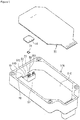
Figure 2 is an isometric view showing the control unit in the input device ofFigure. 1 , with a main board and a sensor board detached; -
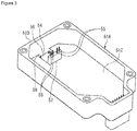
Figure 3 is an isometric view showing the control unit in the input device ofFigure. 1 , with the sensor board loaded in an accommodation region; -
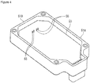
Figure 4 is an isometric view showing the control unit in the input device ofFigure. 1 , with the main board loaded; -
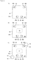
Figures 5(a) to 5(c) are top views showing some forms of the sensor board in the present embodiment, as viewed from a bottom face of the sensor board; -
Figures 6(a) to 6(c) are top views showing some forms of the sensor board in the present embodiment, as viewed from the top face of the sensor board; and -
Figure 7 is a partially-enlarged view ofFigure 1 . - Hereinafter, with reference to the accompanying drawings, an embodiment of the present invention will be described. The present embodiment will be described with reference to an example of using the same for a
brake control unit 50, where a printed circuit board of the present invention is applied to an input device 1 included in a brake system for a vehicle for generating brake fluid pressure according to a manipulated variable of a brake pedal (not shown). The input device 1, as shown inFigure 1 , is provided with abase 10 being a substantially-rectangular-parallelepiped-like enclosure made of a non-magnetic metal material, amaster cylinder 20 for generating brake fluid pressure by brake pedal force, and thebrake control unit 50. Thebrake control unit 50 controls the operation of a motor (not shown) for driving a motor cylinder (not shown) for generating brake fluid pressure, on the basis of information obtained from astroke sensor 70 and/or a pre-stored program or the like. It should be noted that directions, such as top and back or right and left, in the following description are used for convenience in order to describe the input device 1, and they generally correspond to directions when the input device 1 is loaded in a vehicle. The terms should not be considered to limit the invention in any way as other orientations could be used. - The
master cylinder 20, as shown inFigure 1 , is provided with apiston 22 inserted into acylinder cavity 21 of thebase 10, and apermanent magnet 75 provided as a sensed member at a distal end thereof. - The
brake control unit 50, as shown inFigures 1 and2 , has ahousing 51 being a resin enclosure attached to a right side face or top side face 10A1 of thebase 10 of the brake system for a vehicle. Thehousing 51, as shown inFigure 1 , accommodates acontrol board 52 in its internal space. Thehousing 51 is provided with asensor accommodating portion 51F protruding leftward from a face opposite thebase 10. Inside thesensor accommodating portion 51F, anaccommodating recess 58 communicating with the internal space of thehousing 51 is formed. In theaccommodating recess 58, asensor board 54 and thestroke sensor 70 are accommodated. It should be noted that thehousing 51 contains a device, such as a coil C, positioned therein, which is omitted inFigures 2 and3 . - The
housing 51, as shown inFigure 1 , is provided with amain body 51A for accommodating thecontrol board 52 therein, and alid 51B for closing an opening of themain body 51A. Themain body 51A is a member in the shape of an open-topped box, and is integrally formed by injection molding of an electrically-insulating resin. In addition, aconnection terminal 55 for making an electrical connection between themain board 53 and thesensor board 54 of thecontrol board 52 is accommodated in themain body 51A. As shown inFigure 2 , a portion provided for the connection is protrudes into anaccommodating region 56. Theconnection terminal 55 is insert-molded integrally when themain body 51A is produced by injection molding. - The
main body 51A, as shown inFigures 1 and2 , is provided with theaccommodating region 56 for accommodating thesensor board 54. Theaccommodating region 56 is a substantially-rectangular-parallelepiped-like space enclosed with an innerperipheral face 58A of theaccommodating recess 58 opened in abottom face 51C near aside wall 51D. Theaccommodating region 56 has an opening area allowing thesensor board 54 to be accommodated with a suitable gap therearound. In addition, abottom floor 51E inside theaccommodating region 56 is located closer to themaster cylinder 20 than thebottom face 51C of themain body 51A. - The
connection terminal 55 is provided within and beyond theaccommodating region 56. Theconnection terminal 55 is formed of a metal material having excellent conductivity, for example, copper or a copper alloy. In addition, theconnection terminal 55, as shown inFigure 7 , has an L shape on the whole, and is provided with afirst connection portion 551 vertical or perpendicular to thebottom face 51C outside theaccommodating region 56, a buriedportion 552 extending from thefirst connection portion 551 and being parallel to thebottom floor 51E, and asecond connection portion 553 extending from the buriedportion 552 and rising vertically or perpendicularly from thebottom floor 51E. Thefirst connection portion 551 extends through apartition 57 rising at a boundary between theaccommodating recess 58 and thebottom face 51C. Thefirst connection portion 551 and the second connection portion 533 are each provided with an eye-of-needle type press-fit terminal element at their respective distal ends in order to provide a stable electrical connection with themain board 53 and thesensor board 54, respectively. - The
connection terminal 55, as shown inFigure 7 , has thesecond connection portion 553 rising from thebottom floor 51E, and the distal end portion thereof is exposed inside theaccommodating region 56. Theconnection terminal 55 has thefirst connection portion 551 electrically connected with themain board 53, and has thesecond connection portion 553 electrically connected with thesensor board 54. That is, themain board 53 and thesensor board 54 are electrically connected via theconnection terminal 55, so that electric power is supplied from themain board 53 to thesensor board 54 via theconnection terminal 55 and, in addition, a sensing signal of the stroke sensor (magnetic sensing device) 70 is inputted from thesensor board 54 to themain board 53 via theconnection terminal 55. - The present embodiment uses four
connection terminals 55, two of which are exposed in theaccommodating region 56 near theside wall 51D, and the remaining two of which are exposed in theaccommodating region 56 far from theside wall 51D. As shown inFigure 5(a) , fourconnection terminals holes sensor board 54, thereby mechanically supporting thesensor board 54 while themain board 53 and thesensor board 54 are electrically connected. The throughholes connection terminal 55 is written asconnection terminals connection terminal 55 when they do not need to be distinguished. - The
accommodating region 56 has a region between thesensor board 54 and thebottom floor 51E of theaccommodating region 56 shielded from outside to such an extent as to avoid receiving a foreign airborne matter from outside, since thesensor board 54 is supported with theconnection terminals 55 inside theaccommodating region 56, as shown inFigures 1 and3 . Therefore, thestroke sensor 70 mounted on thesensor board 54 positioned in this region avoids receiving a foreign airborne matter from outside. - Next, the
control board 52, as shown inFigures 1 and2 , is composed of themain board 53 and thesensor board 54 arranged hierarchically or lower relative to themain board 53, and thestroke sensor 70 is mounted on thesensor board 54. Thesensor board 54 is positioned between themain board 53 and thebottom floor 51E of theaccommodating region 56, and positioned closer to themain body 51A (bottom floor 51E) of thehousing 51. - The
main board 53, as shown inFigures 1 and4 , is supported with theconnection terminal 55 in the internal space of thehousing 51. Themain board 53 receives an input of information on running conditions fed from the vehicle in addition to a sensed value fed from thestroke sensor 70, and controls each actuator (not shown) of a fluid pressure control device (not shown) for supporting stabilization of behavior of the vehicle on the basis of a stored program. Specifically, themain board 53 controls opening and closing operation of a solenoid valve (not shown) for switching the communication state of an oil path, and/or the number of revolutions of a motor (not shown) for driving a motor cylinder (not shown) for generating brake fluid pressure. - The
sensor board 54, as shown inFigure 7 , is mounted with thestroke sensor 70 on abottom face 54B of a boardmain body 54A and inside thesensor accommodating portion 51F inserted into a groove 10A2 formed in the right side face or top side face 10A1. Thestroke sensor 70, as shown inFigure 1 , is positioned opposite thepermanent magnet 75 of themaster cylinder 20, facing thepermanent magnet 75 across thebase 10 and the peripheral wall of thepiston 22. Thereby, thestroke sensor 70 is positioned at a shortest distance from or close to thepermanent magnet 75 in thehousing 51, and senses forward/backward movement of thepermanent magnet 75, thereby sensing a sliding stroke of thepiston 22. - The
sensor board 54, as shown inFigure 5(a) , has the through-holes connection terminals holes 60A to 60D, a hollow-structured electrical conductor is formed. The hollow-structured electrical conductor is electrically connected with thestroke sensor 70 via a wiring pattern omitted in the drawings. The four through-holes 60A to 60D, in this example, are positioned in the vicinity of vertices of the rectangle. Theconnection terminals holes Figure 5(a) are prevented from interfering with each other. That is, theconnection terminal 55A extends straight in a planar direction, whereas theconnection terminal 55B is so bent in an L-shape near the through-hole 60B as to circumvent theconnection terminal 55A. The same applies to theconnection terminals holes -
Figure 5(b) shows an example of avoiding interference between theconnection terminal 55A and theconnection terminal 55B and between theconnection terminal 55C and theconnection terminal 55D and dispensing with bending of theconnection terminals holes holes holes connection terminals holes connection terminals connection terminals - Next, the
sensor board 54 shown inFigure 5(c) has a shape for enabling theconnection terminals sensor board 54 without making a mistake in the orientation thereof, that is, thesensor board 54 is formed into an asymmetrical planar shape by providing achamfer 54D at one corner of thesensor board 54. On the other hand, in order to make similar a planar shape of theaccommodating region 56 defined by the innerperipheral face 58A of theaccommodating recess 58 to the planar shape of thesensor board 54, an abuttingface 59 for abutting on thechamfer 54D of thesensor board 54 is provided by filling in one corner of the innerperipheral face 58A of theaccommodating recess 58 in a triangular shape, as shown inFigure 2 . Thereby, it is made possible to visually confirm that the orientation of thesensor board 54 is correct when thechamfer 54D at the one corner of thesensor board 54 and the abuttingface 59 provided on the innerperipheral face 58A of theaccommodating region 56 conform to each other, and it is made impossible to press-fit theconnection terminal 55 into thesensor board 54 with a wrong orientation thereof. - Before being installed in the
brake control unit 50, thesensor board 54 undergoes an inspection to ascertain whether or not thesensor board 54 operates properly in addition to programming thestroke sensor 70 of thesensor board 54. Conveniently, when carrying out this process, as shown inFigure 6(a) , anexternal connection pad 63 is provided around each of the through-holes 60A to 60D. Theexternal connection pad 63 is made of a conductive metal material, electrically connected to the electrode provided on the inner periphery of each of the through-holes 60A to 60D, and led out to a predetermined position on atop face 54F of the boardmain body 54A. It should be noted that thestroke sensor 70 is provided on thebottom face 54B of the boardmain body 54A, while theexternal connection pads 63 are provided on thetop face 54F where a mounted component, such as thestroke sensor 70 of thesensor board 54, is not provided. In order to perform processing, such as teaching or programming, thestroke sensor 70 of thesensor board 54, a terminal of a device for performing programming or the like is brought into contact with theexternal connection pads 63 to exchange necessary information exchanged between thestroke sensor 70 and the device. -
Figure 6(b) shows a preferred form of thesensor board 54 taking handling into consideration. Thissensor board 54 is adapted for transportation of thesensor board 54 by air suction, and is provided with asuction face 64 comprising a flat face for being subjected to air suction in thetop face 54F. Thestroke sensor 70 and the wiring pattern for connecting thestroke sensor 70 and the electrodes are not provided on thesuction face 64. For example, by providing all elements, such as thestroke sensor 70 and the electrodes, on the bottom face of thesensor board 54, thesuction face 64 can be provided on thetop face 54F. In addition, with thesuction face 64 provided on thetop face 54F, thestroke sensor 70 and the wiring pattern or the like can also be so provided on thetop face 54F as to avoid thesuction face 64. -
Figure 6(c) shows a form ofsensor board 54 which can be advantageously retained at a fixed position during teaching or programming. Thesensor board 54 has circular-arc-like locating regions regions regions sensor board 54 can be retained at the fixed position. It should be noted that, though the plurality of locating guides 66, 66 and the plurality of locatingregions guide 66 and asingle locating region 65 may be provided. - It should be noted that the
main board 53 is positioned at an interval from or spaced from the right side face or top side face 10A1 of thebase 10 and, as shown inFigure 1 , the coil C or the like is positioned in a space created by the interval. Thesensor board 54 is positioned utilizing such a space for positioning the coil C or the like. In addition, though thestroke sensor 70, inFigure 1 , is shown being proximate to the right side face or the top side face 10A1 of thebase 10, a predetermined gap may be provided between thestroke sensor 70 and the right side face or top side face 10A1. In addition, although thestroke sensor 70 is shown being opposite thepermanent magnet 75 across thebase 10 and the peripheral wall of thepiston 22, thestroke sensor 70 is not limited thereto, but may not be opposite thepermanent magnet 75 in an initial position of themaster cylinder 20 when the brake pedal is not stepped on. - The
sensor board 54 of the present embodiment described above achieves the following advantageous effects. Thesensor board 54 is provided with theexternal connection pads 63 provided on the other face, namely, thetop face 54F, on which thestroke sensor 70 that is a mounted component is not loaded, and electrically connected to the hollow-structured electrical conductors including the through-holes 60A to 60D. Therefore, before thesensor board 54 is press-fitted to theconnection terminals 55 of thehousing 51 and thus loaded, teaching or programming can be performed with the terminal(s) of the teaching or programming device brought into contact with theexternal connection pads 63, and a predetermined inspection can easily be performed with a terminal of an inspection device brought into contact with theexternal connection pads 63. Even when thesensor board 54 fails the inspection, such work as removing thesensor board 54 from thehousing 51 of thebrake control unit 50 is not required. - In addition, the
sensor board 54 is provided with the plurality (four) of through-holes 60A to 60D, and anexternal connection pad 63 is provided for each of the four through-holes 60A to 60D, and moreover, the fourexternal connection pads 63 are electrically independent. Therefore, it is possible to select a suitable one from theexternal connection pads 63 and bring the external terminal into contact therewith to perform necessary processing, including an inspection. - The
sensor board 54 has the four through-holes 60A to 60D formed along a peripheral edge thereof. Therefore, even when external terminals are required to be brought into contact with the plurality ofexternal connection pads 63 in order to perform necessary processing, including an inspection, the external terminals can avoid interfering with each other. In addition, since the four through-holes 60A to 60D are formed at the four corners of thesensor board 54, thesensor board 54 is supported at four points by press-fitting theconnection terminals holes sensor board 54, for example, screw clamping or thermal bonding, is not required. - In addition, the
sensor board 54 is provided with theflat suction face 64 over a predetermined area on a face (the other face) where theexternal connection pads 63 are formed. Therefore, when thesensor board 54 is handled by air suction toward theconnection terminals 55, the suction connection can be reliably secured. - In addition, since the
sensor board 54 is provided with the locatingregions sensor board 54 can easily be located by fitting the locating guides 66, 66 into the locatingregions - Although a preferred embodiment of the present invention has been described above, the present invention is not limited to this embodiment, but can be modified properly within the scope thereof.
- Although the embodiment described above shows an example where four identical
external connection pads 63 are provided, the number of external connection pads in the present invention is not limited and, in addition, the shapes and/or dimensions of the plurality of external connection pads may be different from those described above. - In addition, although the embodiment described above shows an example, as a preferred form, where the
suction face 64 is provided on thetop face 54F of the boardmain body 54A on which a Hall IC is not provided, the present invention allows thesuction face 64 to be provided on a face on which a mounted component, such as a Hall IC, is provided. This form requires thesuction face 64 to be so provided as to avoid a region where such a mounted component is mounted, and therefore, normally, thesuction face 64 is provided at a marginal portion out of the center of thesensor board 54. -
- 10...base
- 10A1...top side face
- 10A2...groove
- 20...master cylinder
- 21...cyclinder cavity
- 22...piston
- 50...brake control unit
- 51...housing
- 51A...main body
- 51B...lid
- 51C...bottom face
- 51D...side wall
- 51E...bottom floor
- 51F...sensor accommodating portion
- 52...control board
- 53...main board
- 54...sensor board
- 54A...board main body
- 54B...bottom face
- 54D...chamfer
- 54F...top face
- 55...connection terminals
- 55A, 55B, 55C, 55D...connection terminal
- 56...accommodating region
- 57...partition
- 58...accommodating recess
- 58A...inner peripheral face
- 59...abutting face
- 60A, 60B, 60C, 60D...through-hole/hollow structured electrical conductors
- 63...external connection pad
- 64...suction face
- 65...locating region
- 66...locating guide
- 70...stroke sensor
- 75...permanent magnet
- 551...first connection portion
- 552...buried portion
- 553 second connection portion
- C...coil
Claims (8)
- A printed circuit board (54) comprising:a board main body (54A) having a magnetic sensing device (70) mounted on at least one of top and bottom faces;an external connection pad (63) provided on the other face opposite to the face on which the magnetic sensing device (70) is mounted; anda hollow-structured electrical conductor (60A, 60B, 60C, 60D) so formed as to extend through the board main body for electrically connecting the magnetic sensing device (70) to the external connection pad (63).
- The printed circuit board (54) according to claim 1, wherein
the board main body (54A) comprises the hollow-structured electrical conductor comprising a plurality of hollow-structured electrical conductors (60A, 60B, 60C, 60D),
the external connection pad (63) is provided for each of the plurality of hollow-structured electrical conductors (60A, 60B, 60C, 60D), and
the plurality of external connection pads (63) are electrically independent. - The printed circuit board (54) according to claim 1 or 2, wherein
the plurality of hollow-structured electrical conductors (60A, 60B, 60C, 60D) are formed along a peripheral edge of the board main body (54A). - The printed circuit board according to any one of claims 1 to 3, wherein
the plurality of hollow-structured electrical conductors (60A, 60B, 60C, 60D) are formed at or near four corners of the board main body (54A). - The printed circuit board according to any one of claims 1 to 4, wherein
the board main body (54A) comprises a flat suction face (64) formed over a predetermined area on the other said face on which the external connection pad (63) is formed. - The printed circuit board (54) according to any one of claims 1 or 5, wherein
the board main body (54A)comprises a locating region (65) corresponding to an external locating guide (66). - The printed circuit board (54) according to any one of claims 1 to 6 wherein each hollow-structured electrical conductor (60A, 60B, 60C, 60D) comprises a through hole.
- The printed circuit board (54) according to claim 7 wherein each hollow-structured electrical conductor (60A, 60B, 60C, 60D) comprises a plated through-hole.
Applications Claiming Priority (1)
| Application Number | Priority Date | Filing Date | Title |
|---|---|---|---|
| JP2017127017A JP6400795B1 (en) | 2017-06-29 | 2017-06-29 | Printed circuit board |
Publications (1)
| Publication Number | Publication Date |
|---|---|
| EP3422825A1 true EP3422825A1 (en) | 2019-01-02 |
Family
ID=62791536
Family Applications (1)
| Application Number | Title | Priority Date | Filing Date |
|---|---|---|---|
| EP18179715.0A Withdrawn EP3422825A1 (en) | 2017-06-29 | 2018-06-26 | Printed circuit board |
Country Status (5)
| Country | Link |
|---|---|
| US (1) | US10959322B2 (en) |
| EP (1) | EP3422825A1 (en) |
| JP (1) | JP6400795B1 (en) |
| KR (1) | KR20190002355A (en) |
| CN (1) | CN109219231A (en) |
Citations (4)
| Publication number | Priority date | Publication date | Assignee | Title |
|---|---|---|---|---|
| JP2003008184A (en) | 2001-06-20 | 2003-01-10 | Toshiba It & Control Systems Corp | Printed board |
| US20160244088A1 (en) * | 2013-09-19 | 2016-08-25 | Hitachi Automotive Systems, Ltd. | Electronic Control Device |
| US9538656B2 (en) * | 2012-02-28 | 2017-01-03 | Electrolux Home Products Corporation N.V. | Electric and/or electronic circuit including a printed circuit board, a separate circuit board and a power connector |
| CN206073906U (en) * | 2016-09-22 | 2017-04-05 | 常州英孚传感科技有限公司 | A kind of brake-pedal-travel sensor |
Family Cites Families (12)
| Publication number | Priority date | Publication date | Assignee | Title |
|---|---|---|---|---|
| JPH0653347A (en) * | 1991-09-30 | 1994-02-25 | Ibiden Co Ltd | Leadless chip carrier |
| JPH0992746A (en) * | 1995-09-26 | 1997-04-04 | Matsushita Electric Works Ltd | Leadless chip carrier |
| TW442945B (en) * | 1998-11-20 | 2001-06-23 | Sony Computer Entertainment Inc | Integrated circuit chip, integrated circuit device, printed circuit board and electronic machine |
| JP2000307056A (en) * | 1999-04-22 | 2000-11-02 | Mitsubishi Electric Corp | Automotive semiconductor devices |
| JP2005172716A (en) * | 2003-12-15 | 2005-06-30 | Hitachi Ltd | Semiconductor module with built-in current sensor |
| JP2009158567A (en) * | 2007-12-25 | 2009-07-16 | Mitsuba Corp | Circuit structure |
| US8659101B2 (en) * | 2010-10-15 | 2014-02-25 | Hitachi Automotive Systems, Ltd. | Physical quantity detector |
| JP5425824B2 (en) * | 2011-02-16 | 2014-02-26 | 日立オートモティブシステムズ株式会社 | Compound sensor |
| JP5852500B2 (en) * | 2012-04-25 | 2016-02-03 | 日立オートモティブシステムズ株式会社 | Electronic control unit |
| JP6157584B2 (en) * | 2013-02-26 | 2017-07-05 | 三菱電機株式会社 | Power semiconductor device embedded device manufacturing method and power semiconductor device |
| JP5945828B2 (en) | 2013-12-05 | 2016-07-05 | 日信工業株式会社 | Brake system input device and vehicle brake system |
| JP6338083B2 (en) | 2013-12-05 | 2018-06-06 | ヴィオニア日信ブレーキシステムジャパン株式会社 | Brake system for vehicles |
-
2017
- 2017-06-29 JP JP2017127017A patent/JP6400795B1/en active Active
-
2018
- 2018-06-26 EP EP18179715.0A patent/EP3422825A1/en not_active Withdrawn
- 2018-06-28 KR KR1020180074723A patent/KR20190002355A/en not_active Abandoned
- 2018-06-29 US US16/022,921 patent/US10959322B2/en active Active
- 2018-06-29 CN CN201810700036.9A patent/CN109219231A/en active Pending
Patent Citations (4)
| Publication number | Priority date | Publication date | Assignee | Title |
|---|---|---|---|---|
| JP2003008184A (en) | 2001-06-20 | 2003-01-10 | Toshiba It & Control Systems Corp | Printed board |
| US9538656B2 (en) * | 2012-02-28 | 2017-01-03 | Electrolux Home Products Corporation N.V. | Electric and/or electronic circuit including a printed circuit board, a separate circuit board and a power connector |
| US20160244088A1 (en) * | 2013-09-19 | 2016-08-25 | Hitachi Automotive Systems, Ltd. | Electronic Control Device |
| CN206073906U (en) * | 2016-09-22 | 2017-04-05 | 常州英孚传感科技有限公司 | A kind of brake-pedal-travel sensor |
Also Published As
| Publication number | Publication date |
|---|---|
| CN109219231A (en) | 2019-01-15 |
| JP2019012716A (en) | 2019-01-24 |
| US20190008034A1 (en) | 2019-01-03 |
| KR20190002355A (en) | 2019-01-08 |
| JP6400795B1 (en) | 2018-10-03 |
| US10959322B2 (en) | 2021-03-23 |
Similar Documents
| Publication | Publication Date | Title |
|---|---|---|
| US6317332B1 (en) | Electronic module for an electric motor operated drive unit | |
| KR100592978B1 (en) | Current sensor with magnetic gap | |
| US8112196B2 (en) | Electronic control unit and vehicle behavior control device | |
| US10634702B2 (en) | Current sensor | |
| US10106136B2 (en) | Electronic control unit assembling method, electronic control unit and vehicle brake hydraulic pressure control apparatus | |
| KR101834092B1 (en) | Lead frame, electronic control device using lead frame, and lead-frame mounting method | |
| US11167740B2 (en) | Coil assembly and brake control device | |
| CN108778867B (en) | Electronic control device | |
| US6724578B2 (en) | Electrical connection for the actuator coil of a magnetic disk drive | |
| CN111316505B (en) | circuit device | |
| JP2016528663A (en) | Electric appliance for establishing electric transmission between printed circuit board and motor | |
| JP6954774B2 (en) | Controller unit | |
| EP3422825A1 (en) | Printed circuit board | |
| US10653020B2 (en) | Electronic module and method for producing an electronic module | |
| CN109219246B (en) | packaged integrated circuit components | |
| CN108023014B (en) | Electronic component | |
| US9381898B2 (en) | Actuator for brake fluid pressure control | |
| CN113891589B (en) | Cable with resin molded body | |
| CN114630486A (en) | Circuit board assembly, component assembly for positioning current sensor and mounting method | |
| EP3499249A1 (en) | Electronic component | |
| CN115866957B (en) | Circuit structure and electrical connection box | |
| JP2000022301A (en) | Electronic component mounting substrate, position detecting substrate, position detecting device, electronic component mounting method, and method of manufacturing position detecting device | |
| CN100460248C (en) | electronic device | |
| JP2001196762A (en) | Power source unit and its manufacturing method | |
| CN120753010A (en) | Display unit for an automation field device |
Legal Events
| Date | Code | Title | Description |
|---|---|---|---|
| PUAI | Public reference made under article 153(3) epc to a published international application that has entered the european phase |
Free format text: ORIGINAL CODE: 0009012 |
|
| STAA | Information on the status of an ep patent application or granted ep patent |
Free format text: STATUS: THE APPLICATION HAS BEEN PUBLISHED |
|
| AK | Designated contracting states |
Kind code of ref document: A1 Designated state(s): AL AT BE BG CH CY CZ DE DK EE ES FI FR GB GR HR HU IE IS IT LI LT LU LV MC MK MT NL NO PL PT RO RS SE SI SK SM TR |
|
| AX | Request for extension of the european patent |
Extension state: BA ME |
|
| STAA | Information on the status of an ep patent application or granted ep patent |
Free format text: STATUS: REQUEST FOR EXAMINATION WAS MADE |
|
| 17P | Request for examination filed |
Effective date: 20190604 |
|
| RBV | Designated contracting states (corrected) |
Designated state(s): AL AT BE BG CH CY CZ DE DK EE ES FI FR GB GR HR HU IE IS IT LI LT LU LV MC MK MT NL NO PL PT RO RS SE SI SK SM TR |
|
| STAA | Information on the status of an ep patent application or granted ep patent |
Free format text: STATUS: THE APPLICATION IS DEEMED TO BE WITHDRAWN |
|
| 18D | Application deemed to be withdrawn |
Effective date: 20210112 |