EP3422394A1 - Apparatus and method for processing a semiconductor substrate - Google Patents
Apparatus and method for processing a semiconductor substrate Download PDFInfo
- Publication number
- EP3422394A1 EP3422394A1 EP17178590.0A EP17178590A EP3422394A1 EP 3422394 A1 EP3422394 A1 EP 3422394A1 EP 17178590 A EP17178590 A EP 17178590A EP 3422394 A1 EP3422394 A1 EP 3422394A1
- Authority
- EP
- European Patent Office
- Prior art keywords
- semiconductor substrate
- semiconductor
- layer
- base plate
- bending tool
- Prior art date
- Legal status (The legal status is an assumption and is not a legal conclusion. Google has not performed a legal analysis and makes no representation as to the accuracy of the status listed.)
- Granted
Links
Images


Classifications
-
- H—ELECTRICITY
- H10—SEMICONDUCTOR DEVICES; ELECTRIC SOLID-STATE DEVICES NOT OTHERWISE PROVIDED FOR
- H10P—GENERIC PROCESSES OR APPARATUS FOR THE MANUFACTURE OR TREATMENT OF DEVICES COVERED BY CLASS H10
- H10P72/00—Handling or holding of wafers, substrates or devices during manufacture or treatment thereof
- H10P72/04—Apparatus for manufacture or treatment
- H10P72/0428—Apparatus for mechanical treatment or grinding or cutting
-
- H—ELECTRICITY
- H10—SEMICONDUCTOR DEVICES; ELECTRIC SOLID-STATE DEVICES NOT OTHERWISE PROVIDED FOR
- H10P—GENERIC PROCESSES OR APPARATUS FOR THE MANUFACTURE OR TREATMENT OF DEVICES COVERED BY CLASS H10
- H10P72/00—Handling or holding of wafers, substrates or devices during manufacture or treatment thereof
- H10P72/04—Apparatus for manufacture or treatment
- H10P72/0446—Apparatus for mounting on conductive members, e.g. leadframes or conductors on insulating substrates
-
- H—ELECTRICITY
- H10—SEMICONDUCTOR DEVICES; ELECTRIC SOLID-STATE DEVICES NOT OTHERWISE PROVIDED FOR
- H10W—GENERIC PACKAGES, INTERCONNECTIONS, CONNECTORS OR OTHER CONSTRUCTIONAL DETAILS OF DEVICES COVERED BY CLASS H10
- H10W40/00—Arrangements for thermal protection or thermal control
- H10W40/20—Arrangements for cooling
- H10W40/25—Arrangements for cooling characterised by their materials
- H10W40/255—Arrangements for cooling characterised by their materials having a laminate or multilayered structure, e.g. direct bond copper [DBC] ceramic substrates
-
- H—ELECTRICITY
- H10—SEMICONDUCTOR DEVICES; ELECTRIC SOLID-STATE DEVICES NOT OTHERWISE PROVIDED FOR
- H10W—GENERIC PACKAGES, INTERCONNECTIONS, CONNECTORS OR OTHER CONSTRUCTIONAL DETAILS OF DEVICES COVERED BY CLASS H10
- H10W70/00—Package substrates; Interposers; Redistribution layers [RDL]
- H10W70/01—Manufacture or treatment
- H10W70/02—Manufacture or treatment of conductive package substrates serving as an interconnection, e.g. of metal plates
- H10W70/027—Mechanical treatments, e.g. deforming, punching or cutting
-
- H—ELECTRICITY
- H10—SEMICONDUCTOR DEVICES; ELECTRIC SOLID-STATE DEVICES NOT OTHERWISE PROVIDED FOR
- H10W—GENERIC PACKAGES, INTERCONNECTIONS, CONNECTORS OR OTHER CONSTRUCTIONAL DETAILS OF DEVICES COVERED BY CLASS H10
- H10W70/00—Package substrates; Interposers; Redistribution layers [RDL]
- H10W70/20—Conductive package substrates serving as an interconnection, e.g. metal plates
-
- H—ELECTRICITY
- H10—SEMICONDUCTOR DEVICES; ELECTRIC SOLID-STATE DEVICES NOT OTHERWISE PROVIDED FOR
- H10W—GENERIC PACKAGES, INTERCONNECTIONS, CONNECTORS OR OTHER CONSTRUCTIONAL DETAILS OF DEVICES COVERED BY CLASS H10
- H10W70/00—Package substrates; Interposers; Redistribution layers [RDL]
- H10W70/60—Insulating or insulated package substrates; Interposers; Redistribution layers
- H10W70/67—Insulating or insulated package substrates; Interposers; Redistribution layers characterised by their insulating layers or insulating parts
- H10W70/68—Shapes or dispositions thereof
-
- H—ELECTRICITY
- H10—SEMICONDUCTOR DEVICES; ELECTRIC SOLID-STATE DEVICES NOT OTHERWISE PROVIDED FOR
- H10W—GENERIC PACKAGES, INTERCONNECTIONS, CONNECTORS OR OTHER CONSTRUCTIONAL DETAILS OF DEVICES COVERED BY CLASS H10
- H10W72/00—Interconnections or connectors in packages
- H10W72/071—Connecting or disconnecting
- H10W72/0711—Apparatus therefor
-
- H—ELECTRICITY
- H10—SEMICONDUCTOR DEVICES; ELECTRIC SOLID-STATE DEVICES NOT OTHERWISE PROVIDED FOR
- H10P—GENERIC PROCESSES OR APPARATUS FOR THE MANUFACTURE OR TREATMENT OF DEVICES COVERED BY CLASS H10
- H10P72/00—Handling or holding of wafers, substrates or devices during manufacture or treatment thereof
- H10P72/70—Handling or holding of wafers, substrates or devices during manufacture or treatment thereof for supporting or gripping
- H10P72/74—Handling or holding of wafers, substrates or devices during manufacture or treatment thereof for supporting or gripping using temporarily an auxiliary support
- H10P72/743—Handling or holding of wafers, substrates or devices during manufacture or treatment thereof for supporting or gripping using temporarily an auxiliary support used as a support during manufacture of interconnect decals or build up layers
-
- H—ELECTRICITY
- H10—SEMICONDUCTOR DEVICES; ELECTRIC SOLID-STATE DEVICES NOT OTHERWISE PROVIDED FOR
- H10W—GENERIC PACKAGES, INTERCONNECTIONS, CONNECTORS OR OTHER CONSTRUCTIONAL DETAILS OF DEVICES COVERED BY CLASS H10
- H10W72/00—Interconnections or connectors in packages
- H10W72/071—Connecting or disconnecting
- H10W72/0711—Apparatus therefor
- H10W72/07141—Means for applying energy, e.g. ovens or lasers
Definitions
- the instant disclosure relates to an apparatus and a method for processing a semiconductor substrate, in particular a semiconductor substrate for a power semiconductor module arrangement.
- Power semiconductor module arrangements often include a base plate within a housing. At least one substrate is arranged on the base plate. A semiconductor arrangement including a plurality of controllable semiconductor elements (e.g., two IGBTs in a half-bridge configuration) is arranged on each of the at least one substrate. Each substrate usually comprises a substrate layer (e.g., a ceramic layer), a first metallization layer deposited on a first side of the substrate layer and a second metallization layer deposited on a second side of the substrate layer. The controllable semiconductor elements are mounted, for example, on the first metallization layer. The second metallization layer is usually attached to the base plate.
- a substrate layer e.g., a ceramic layer
- the controllable semiconductor elements are mounted, for example, on the first metallization layer.
- the second metallization layer is usually attached to the base plate.
- the semiconductor devices When mounting the controllable semiconductor devices to the substrate, e.g., by soldering or sintering, the semiconductor devices are usually pressed onto the first metallization layer with a certain amount of force and under the influence of high temperatures, wherein the temperatures usually lie at about 300° C, sometimes even 500°C and more. This leads to a deformation of the substrate, usually a convex deflection in the direction of the first metallization layer on which the semiconductor elements are mounted.
- Base plates are usually manufactured to have a concave deflection in the direction of the surface on which the one or more substrates are to be mounted. The deflection of the base plate, therefore, is opposite to the deflection of the substrate.
- a connection layer is arranged between the base plate and the substrate.
- Such a connection layer usually completely fills the space between the base plate and the substrate and therefore has a non-uniform thickness because of the opposite deflections of the substrate and the base plate.
- the thickness of the connection layer influences the heat conduction as well as other parameters.
- the grade of deformation of the substrate as well as of the base plate may vary between different substrates and base plates and is usually not predictable, which may lead to unpredictable thicknesses of the connection layer and to an unpredictable thermal conduction. This may limit the reliability of the semiconductor arrangement and the whole power semiconductor module arrangement.
- a method includes placing a semiconductor substrate on a first curved surface of a first bending tool, using a second bending tool with a second surface to apply pressure to the semiconductor substrate, thereby pressing the semiconductor substrate onto the first curved surface and bending the semiconductor substrate, and removing the bended semiconductor substrate from the first bending tool.
- An apparatus includes a first bending tool with a first curved surface and a second bending tool with a second surface.
- the second bending tool is configured to apply pressure to a semiconductor substrate that is arranged on the first curved surface, thereby pressing the semiconductor substrate onto the first curved surface and bending the semiconductor substrate.
- An electrical line or electrical connection as described herein may be a single electrically conductive element, or include at least two individual electrically conductive elements connected in series and/or parallel. Electrical lines and electrical connections may include metal and/or semiconductor material, and may be permanently electrically conductive (i.e., non-switchable).
- a semiconductor body as described herein may be made from (doped) semiconductor material and may be a semiconductor chip or be included in a semiconductor chip. A semiconductor body has electrically connecting pads and includes at least one semiconductor element with electrodes.
- the semiconductor substrate 10 includes a dielectric insulation layer 11, a (structured) first metallization layer 111 attached to the dielectric insulation layer 11, and a second (structured) metallization layer 112 attached to the dielectric insulation layer 11.
- the dielectric insulation layer 11 is disposed between the first and second metallization layers 111, 112.
- Each of the first and second metallization layers 111, 112 may consist of or include one of the following materials: copper; a copper alloy; aluminium; an aluminium alloy; any other metal or alloy that remains solid during the operation of the power semiconductor module arrangement.
- the semiconductor substrate 10 may be a ceramic substrate, that is, a substrate in which the dielectric insulation layer 11 is a ceramic, e.g., a thin ceramic layer.
- the ceramic may consist of or include one of the following materials: aluminium oxide; aluminium nitride; zirconium oxide; silicon nitride; boron nitride; or any other dielectric ceramic.
- the dielectric insulation layer 11 may consist of or include one of the following materials: Al 2 O 3 , AlN, or Si 3 N 4 .
- the substrate 10 may, e.g., be a Direct Copper Bonding (DCB) substrate, a Direct Aluminium Bonding (DAB) substrate, or an Active Metal Brazing (AMB) substrate.
- the substrate 10 may also be a conventional printed circuit board (PCB) having a non-ceramic dielectric insulation layer 11.
- a non-ceramic dielectric insulation layer 11 may consist of or include a cured resin.
- One or more semiconductor bodies 20 may be arranged on the semiconductor substrate 10.
- Each of the semiconductor bodies 20 arranged on the semiconductor substrate 10 may include an IGBT (Insulated-Gate Bipolar Transistor), a MOSFET (Metal-Oxide-Semiconductor Field-Effect Transistor), a JFET (Junction Field-Effect Transistor), a HEMT (High-Electron-Mobility Transistor), or any other suitable controllable semiconductor element.
- IGBT Insulated-Gate Bipolar Transistor
- MOSFET Metal-Oxide-Semiconductor Field-Effect Transistor
- JFET Joint Field-Effect Transistor
- HEMT High-Electron-Mobility Transistor
- the one or more semiconductor bodies 20 may form a semiconductor arrangement on the semiconductor substrate 10.
- the first metallization layer 111 of Figure 1 is a continuous layer.
- the first metallization layer 111 may be structured, for example if more than one semiconductor body 20 is mounted to the semiconductor substrate 10.
- "Structured metallization layer” means that the first metallization layer 111 is not a continuous layer, but includes recesses between different sections of the layer. Such recesses are schematically illustrated, for example, in Figure 6C , where the first metallization layer 111 includes three different sections. Different semiconductor bodies 20 may be mounted to the same or to different sections of the first metallization layer 111.
- Different sections of the first metallization layer may have no electrical connection or may be electrically connected to one or more other sections using, e.g., bonding wires 21.
- An electrical connection (bonding wire 21) which electrically connects the semiconductor body on one section of the first metallization layer 111 with another section of the first metallization layer 111 is schematically illustrated in Figure 6C in a dashed line.
- the one or more semiconductor bodies 20 may be electrically and mechanically connected to the semiconductor substrate 10 by an electrically conductive connection layer (not illustrated in Figure 1 ).
- Such an electrically conductive connection layer may be a solder layer, a layer of an electrically conductive adhesive, or a layer of a sintered metal powder, e.g., a sintered silver powder, for example.
- the substrate When mounting the one or more semiconductor bodies 20 to the substrate 10, the substrate is usually placed on a contact surface of a first mounting tool 31.
- the semiconductor bodies 20 are arranged on the substrate surface (top surface) and are then pressed onto the substrate 10 using a second mounting tool 32.
- Appropriate methods for mounting a semiconductor body 20 to a semiconductor substrate 10 such as, e.g., soldering methods or sintering methods, are commonly known and will not be described in further detail.
- the substrate 10, the semiconductor bodies 20 as well as a contact layer (not illustrated) between the substrate 10 and the semiconductor bodies 20 are usually heated during such mounting process, e.g., a sintering process.
- the temperature during the mounting of the semiconductor bodies 20 may be more than 200° C, more than 300° C, or more than 400° C, for example.
- the substrate 10 with the semiconductor bodies 20 mounted thereon is permanently bended and usually has a convex deflection in the direction of the first metallization layer 111 on which the semiconductor bodies 20 are mounted. This convex deflection or curvature is exemplarily illustrated in Figure 2A .
- the dashed lines in Figure 2A merely serve to illustrate the deflections of the different elements illustrated therein.
- the deflection of the semiconductor substrate 10 or, in other words, the deviation from its original (essentially plane) form may be, e.g., between about 100 ⁇ m and about 500 ⁇ m (difference in height between the edges and the center of the semiconductor substrate).
- the base plate 40 may have a thickness of between about 1mm and about 6mm, for example.
- the base plate 40 may also be thinner than 1mm or thicker than 6mm.
- the base plate 40 may consist of or include a metal or a metal matrix composite material (e.g., metal matrix composite MMC such as aluminium silicon carbide), for example. Suitable materials for a metal base plate 40 are, for example, copper, a copper alloy, aluminium, or an aluminium alloy.
- the base plate 40 may be coated by a thin coating layer (not illustrated). Such a coating layer may consist of or include nickel, silver, gold, or palladium, for example.
- the coating layer is optional and may improve the solderability of the base plate 40.
- the base plate 40 may be arranged in a housing (not illustrated).
- the at least one substrate 10 may be electrically and mechanically connected to the base plate 40 by a first connection layer 50.
- the first connection layer 50 may be a solder layer, a layer of an electrically conductive adhesive, or a layer of a sintered metal powder, e.g., a sintered silver powder, for example.
- a semiconductor module 10 that is mounted on a base plate 40 is exemplarily illustrated in Figure 2B .
- the base plate 40 usually has a deflection. The deflection of the base plate 40 is generally opposite to the deflection of the semiconductor substrate 10.
- the base plate 40 has a concave deflection in the direction of the surface on which the one or more base plates 40 are mounted, as is illustrated in Figure 2 .
- the deflection of the base plate 40 or, in other words, the deviation from its original (essentially plane) form, may be in the same order as the deflection of the semiconductor substrate, namely between about 100 ⁇ m and about 500 ⁇ m, for example (difference in height between the edges and the center of the base plate).
- the examples illustrated herein describe a semiconductor substrate 10 that is mounted on a base plate 40. This is, however only an example. In some power semiconductor module arrangements, the semiconductor substrate 10 is not mounted to a base plate 40. Instead of to a base plate 40, the semiconductor substrate 10 may be mounted to a heat sink (not illustrated), for example. A layer of heat-conducting paste may be arranged between the semiconductor substrate 10 and the heat sink, for example. Mounting the semiconductor substrate 10 to a base plate 40 or a heat sink are, however, only examples. Generally, the semiconductor substrate 10 may be mounted to any suitable device or entity of a power semiconductor module arrangement.
- the semiconductor substrate 10 may be deflected in one direction in space only. However, as is schematically illustrated in Figure 3 , the semiconductor substrate 10 may also be deflected in two directions in space, resulting in a cushion-shape or shell-like shape of the substrate 10. The same applies for the base plate 40.
- the first connection layer 50 may have a varying thickness.
- the thickness of the first connection layer 50 may be greater below the center of the semiconductor substrate 10 and may be smaller near the edges of the semiconductor substrate 10. In areas where the first connection layer 50 has a great thickness, the thermal resistance may be poor. The thinner the first connection layer 50, the lower the thermal resistance and the better the power density.
- the thickness of the first connection layer 50 may vary greatly for different power semiconductor modules. This is because the deflection of the semiconductor substrate 10 and of the base plate 40 currently cannot be reliably manipulated and may vary greatly between different substrates and base plates.
- a homogenous first connection layer 50 usually provides a better thermal resistance for the power semiconductor module which may lead to an increased reliability of the power semiconductor module.
- One method includes the positioning of spacers 51 between the semiconductor substrate 10 and the base plate 40, as is schematically illustrated in Figure 4 .
- the semiconductor substrate 10 is pressed onto the base plate 40 or, more particularly, onto the one or more spacers 51 with great force F10.
- one or more weights may be placed on top of the semiconductor substrate 10 to bend the semiconductor substrate 10 in the direction of the base plate 40 until it reaches the spacers 51. After the bending the semiconductor substrate may have essentially the same deflection as the base plate 40.
- the weights may be in the range of several 100g, for example, and may apply a very selective force to only some areas of the semiconductor substrate 10. The force, therefore, is not evenly distributed over the surface of the semiconductor substrate 10. Placing rather heavy weights on the semiconductor substrate 10, thereby bending the semiconductor substrate 10 in the direction of the base plate 40, leads to an essentially homogenous first connection layer 50. However, the semiconductor substrate 10 and the semiconductor bodies 20 mounted thereon are subjected to a great, selective force F10 and may be severely damaged during the mounting process. Furthermore, the heavy weights usually need to be handled manually, which may lead to physical harm of the operating personnel when many weights need to be handled. Another drawback lies in the fact that placing heavy weights (e.g., > 100g) on the semiconductor substrate 10 alters the thermal capacity of the soldering forms that are used for mounting the semiconductor substrates 10 to the base plates 40 during a soldering process.
- heavy weights e.g., > 100g
- the present invention tries to avoid the exertion of a great force when mounting the semiconductor substrate 10 onto the base plate 40, thereby reducing the risk of damages of the semiconductor substrate 10 and the semiconductor bodies 20 mounted thereon. Further, the deflection of the semiconductor substrates 10 may be more reliably adjusted such that it varies less between different semiconductor substrates 10.
- an apparatus for processing a semiconductor substrate 10 includes a first bending tool 33 and a second bending tool 34.
- the first bending tool 33 comprises a first curved surface 303, e.g., a curved top surface.
- the second bending tool 34 comprises a second curved surface 304, e.g., a bottom surface.
- the first curved surface 303 may be a concave surface or a convex surface, for example.
- the deflection of the second curved surface 304 may be opposite to the deflection of the first curved surface 303.
- the second curved surface 304 may be a convex surface if the first curved surface is a concave surface, and vice versa.
- a semiconductor substrate 10 may be arranged between the first bending tool 33 and the second bending tool 34.
- the semiconductor substrate 10 may be placed on the first curved surface 303.
- the second metallization layer 112 that is to be mounted to the base plate 40 faces the first curved surface 303 and the first metallization layer 111 on which the one or more semiconductor bodies are to be mounted faces the second curved surface 304.
- the first curved surface 303 may be curved in only one direction of space to generate a deflection of the semiconductor substrate 10 in only one direction. However, it is also possible that the first curved surface 303 is curved in two directions of space, e.g., pillow-shaped or shell-like shape, to generate a deflection of the semiconductor substrate 10 in two directions as has been described with reference to Figure 3 before. The same applies for the second curved surface 304.
- the second bending tool 34 may apply pressure (a force) to the semiconductor substrate 10, as is schematically illustrated in Figure 5B .
- the semiconductor substrate 10 adapts to the shape of the first and the second bending tool 33, 34.
- the semiconductor substrate 10 may additionally be heated.
- the semiconductor substrate 10 may be heated to up to 200° C, to up to 300° C, to up to 400° C, or to up to 500° C. Heating the semiconductor substrate 10, however, is optional.
- the process may also be performed at room temperature, for example.
- the deflection of the first bending tool 33 and the second bending tool 34 may be in the same dimension as the desired deflection of the semiconductor substrate 10, for example.
- the first bending tool 33 may have a deflection of, e.g., between about 100 ⁇ m and about 500 ⁇ m (difference in height between the edges/corners and the center of the first curved surface 303).
- the second bending tool 34 may also have a deflection of, e.g., between about 100 ⁇ m and about 500 ⁇ m.
- the deflection of the first bending tool 33 may be in the same order as the deflection of the second bending tool 34, with the only difference that the orientation of the deflection is opposite to the orientation of the deflection of the first bending tool 33 (e.g., first bending tool 33 concave, second bending tool 34 convex, or vice versa).
- an essentially homogenous first connection layer 50 may be obtained during a following soldering process during which the semiconductor substrate 10 is mounted to the base plate 40.
- Essentially homogenous in this context means that the thickness of the first connection layer 50 has a deviation of, e.g., maximally ⁇ 25 ⁇ m, maximally ⁇ 50 ⁇ m, or maximally ⁇ 75 ⁇ m of the average thickness over the entire area.
- the thickness of the first connection layer 50 has a deviation of, e.g., maximally ⁇ 13 ⁇ m of the average thickness over the entire area. Other greater or smaller deviations are also possible.
- the deflection of the semiconductor substrate 10, however, may also differ from the deflection of the base plate 40, e.g., be greater or smaller than the deflection of the base plate 40. In this way, a first connection layer 50 may be obtained which has a greater thickness at the center of the semiconductor substrate 10 and a smaller thickness near the edges/corners of the semiconductor substrate 10. Or a first connection layer 50 may be obtained which has a smaller thickness at the center of the semiconductor substrate 10 and a greater thickness near the edges/corners of the semiconductor substrate 10.
- the thickness of the first connection layer 50 near the edges/corners (below the edges/corners) of the semiconductor substrate 10 may be 50 ⁇ m or more than 50 ⁇ m thinner than the thickness at the center (below the center) of the semiconductor substrate 10.
- typical average thicknesses of the first connection layer 50 may be between about 200 ⁇ m and about 600 ⁇ m.
- a typical average thickness of down to about 50 ⁇ m is also possible.
- the thickness of the first connection layer 50 may be reliably adjusted by pre-bending the semiconductor substrate 10. By reliably adjusting the thickness of the first connection layer 50, the reliability of the semiconductor arrangement arranged on the semiconductor substrate 10 as well as the reliability of the whole power semiconductor module arrangement may be increased.
- the second bending tool 34 has a surface area which is greater than the surface area of the semiconductor substrate 10. This means that during the bending process, while the second bending tool 34 applies a pressure to the semiconductor substrate 10, the second bending tool 34 completely covers the semiconductor substrate 10. This is, however, only an example.
- the second bending tool 34 may have a surface area which is smaller than the surface area of the semiconductor substrate 10. This means that during the bending process, while the second bending tool 34 applies a pressure to the semiconductor substrate 10, the second bending tool 34 does not completely cover the semiconductor substrate 10. In this example, the second bending tool 34 only partly covers the semiconductor substrate 10. For example, the second bending tool 34 may apply a pressure only on a central part of the semiconductor substrate 10, while no pressure is applied near the edges of the semiconductor substrate 10.
- the second bending tool 34 that is illustrated in the Figures has a continuous surface. This is, however, only an example.
- the second bending tool 34 may also include several parts (so-called multi-stamp tool). For example, a first part may apply a pressure to a central region of the semiconductor substrate 10, a second part may apply a pressure to an edge region of the semiconductor substrate 10, and a third part may apply a pressure to a region in between the central region and the edge region. There may be areas of the semiconductor substrate 10, to which no pressure is applied directly. In other words, pressure may be applied selectively to different areas of the semiconductor substrate 10.
- the semiconductor substrate 10 is (permanently) bended (curved).
- a bended semiconductor substrate 10 is exemplarily illustrated in Figure 5C .
- one or more semiconductor bodies 20 may be mounted to the bended semiconductor substrate 10.
- the semiconductor bodies 20 may be soldered onto the semiconductor substrate 10, for example. Soldering processes for mounting semiconductor bodies 20 on a semiconductor substrate 10 are generally known and will not be described in further detail.
- the semiconductor substrate 10 may be mounted to a base plate 40.
- one or more spacers 51 may be arranged between the base plate 40 and the semiconductor substrate 10.
- the one or more spacers form an end stop for the semiconductor substrate 10 during a soldering process.
- a homogenous first connection layer 50 between the semiconductor substrate 10 and the base plate 40 may be obtained.
- the height as well as the number of spacers 51 defines the thickness of the first connection layer 50.
- the spacers 51 may be separate elements that are mounted to the base plate 40 by any appropriate means.
- the spacers 51 are integral parts of the base plate 40, e.g., protrusions or projections. Such spacers 51, however, are optional.
- the deflection of the semiconductor substrate 10 may essentially correspond to the deflection of the base plate 40.
- the deflection of the semiconductor substrate 10 essentially corresponds to the deflection of the base plate 40, it is no longer necessary to apply a great force to the semiconductor substrate 10, as has been described with reference to Figure 4 before. It is no longer necessary to further bend the semiconductor substrate 10 during the step of mounting the semiconductor substrate 10 to the base plate 40, because the semiconductor substrate 10 is already pre-bended to have a concave deflection.
- the deflection of the semiconductor substrate 10 essentially corresponds to the deflection of the base plate 40 and, therefore, a comparatively small force F11 is necessary to press the semiconductor substrate 10 to the base plate 40.
- small weights may be placed on top of the semiconductor substrate 10, to press the semiconductor substrate 10 onto the base plate 40.
- the small weights that are placed on the semiconductor substrate 10 may be in the range of 10g or up to several 10g, for example.
- the weights that are placed on the semiconductor substrate 10 are only needed to fixate the semiconductor substrate 10 in place to keep the desired orientation of the semiconductor substrate 10.
- Figure 6 schematically illustrates another method for processing a semiconductor substrate 10.
- the semiconductor bodies 20 are, e.g., sintered to the semiconductor substrate 10 instead of soldered, it is possible to mount the semiconductor bodies 20 to the semiconductor substrate 10 while bending the semiconductor substrate 10.
- the semiconductor substrate 10 may be placed on the first curved surface 303 of the first bending tool 33.
- one or more semiconductor bodies 20 may be arranged between the semiconductor substrate 10 and the second bending tool 34.
- a layer of a metal powder, e.g., a silver powder, (not illustrated in Figure 6 ) may be arranged between the semiconductor bodies 20 and the semiconductor substrate 10, for example.
- the second bending tool 34 may have a second curved surface 304, as has been described with respect to Figure 5 before.
- the second bending tool 34 has a flat, or plane surface, as is schematically illustrated in Figure 6 .
- a layer of compensatory material 60 may be arranged between the semiconductor substrate 10 with the semiconductor bodies 20 and the second (curved or plane) surface 304.
- the layer of compensatory material 60 may be configured to distribute the force that is applied by the second bending tool 34 evenly over the semiconductor substrate 10 and the semiconductor bodies 20 arranged thereon.
- the layer of compensatory material 60 may consist of or comprise any material that is suitable to adjust any differences between the contours of the second (curved) surface 304 and the semiconductor substrate 10, or, more precisely, between the contours of the second (curved) surface 304 and the semiconductor substrate 10 in its desired form (its bended form).
- a layer of compensatory material 60 may generally also be used for the method that is described referring to Figure 5 above. Even if no semiconductor bodies are (yet) arranged on the semiconductor substrate 10, the layer of compensatory material 60 may distribute the pressure that is applied by the second bending tool 34 evenly over the semiconductor substrate 10. The layer of compensatory material 60 may be attached to the second surface 304, for example. According to another example, the layer of compensatory material 60 is a foil that is inserted between the semiconductor substrate 10 and the second bending tool 34.
- a flat (plane) second surface 304 is only an example. It is also possible that the second bending tool 34 has a second curved surface 304, as has been described with respect to Figure 5 before. If the second bending tool 34 comprises a second curved surface 304, the layer of compensatory material 60 is optional and may be omitted.
- the semiconductor bodies 20 may, at the same time, be sintered to the semiconductor substrate 10.
- the semiconductor substrate 10 may be heated during the sintering and bending process.
- the semiconductor substrate 10 may be heated to up to 200° C, to up to 300° C, to up to 400° C or to up to 500° C. Sinter processes are generally known and will not be described in further detail.
- a method for processing (pre-bending) a semiconductor substrate 10 includes the step of arranging the semiconductor substrate 10 on a first curved surface 303 of a first bending tool 33. Pressure may be applied to the semiconductor substrate 10 by using a second bending tool 34 with a second surface 304. The semiconductor substrate 10 is thereby pressed onto the first curved surface 303 and is thereby pre-bended.
- the second surface 304 may be a flat surface or a curved surface. If semiconductor bodies 20 are to be soldered to the semiconductor substrate 10, a soldering process may follow after pre-bending the semiconductor substrate 10. This means that semiconductor bodies 20 are soldered on the bended semiconductor substrate 10.
- a sintering process may be performed while bending the semiconductor substrate 10.
- a sintering process usually includes applying a certain pressure to the semiconductor bodies 20 and may be performed at the same time while the semiconductor substrate 10 is pre-bended.
- the semiconductor substrate 10 is removed from the first bending tool 33.
- the semiconductor substrate 10 does not have a permanent connection to the first bending tool33 and is not permanently mounted to the first bending tool 33.
- the semiconductor substrate 10 may be mounted to (e.g., soldered to) a base plate 40.
- Power semiconductor module arrangements often include a base plate 40 (with at least one semiconductor substrate 10 mounted thereon) within a housing.
- the first bending tool 33 and the second bending tool 34 are not components of such a power semiconductor module arrangement.
Landscapes
- Cooling Or The Like Of Semiconductors Or Solid State Devices (AREA)
- Chemical & Material Sciences (AREA)
- Engineering & Computer Science (AREA)
- Ceramic Engineering (AREA)
Abstract
Description
- The instant disclosure relates to an apparatus and a method for processing a semiconductor substrate, in particular a semiconductor substrate for a power semiconductor module arrangement.
- Power semiconductor module arrangements often include a base plate within a housing. At least one substrate is arranged on the base plate. A semiconductor arrangement including a plurality of controllable semiconductor elements (e.g., two IGBTs in a half-bridge configuration) is arranged on each of the at least one substrate. Each substrate usually comprises a substrate layer (e.g., a ceramic layer), a first metallization layer deposited on a first side of the substrate layer and a second metallization layer deposited on a second side of the substrate layer. The controllable semiconductor elements are mounted, for example, on the first metallization layer. The second metallization layer is usually attached to the base plate. When mounting the controllable semiconductor devices to the substrate, e.g., by soldering or sintering, the semiconductor devices are usually pressed onto the first metallization layer with a certain amount of force and under the influence of high temperatures, wherein the temperatures usually lie at about 300° C, sometimes even 500°C and more. This leads to a deformation of the substrate, usually a convex deflection in the direction of the first metallization layer on which the semiconductor elements are mounted.
- Base plates are usually manufactured to have a concave deflection in the direction of the surface on which the one or more substrates are to be mounted. The deflection of the base plate, therefore, is opposite to the deflection of the substrate. When mounting the substrate to the base plate, a connection layer is arranged between the base plate and the substrate. Such a connection layer usually completely fills the space between the base plate and the substrate and therefore has a non-uniform thickness because of the opposite deflections of the substrate and the base plate. The thickness of the connection layer influences the heat conduction as well as other parameters. The grade of deformation of the substrate as well as of the base plate may vary between different substrates and base plates and is usually not predictable, which may lead to unpredictable thicknesses of the connection layer and to an unpredictable thermal conduction. This may limit the reliability of the semiconductor arrangement and the whole power semiconductor module arrangement.
- There is a need for a semiconductor substrate that avoids the drawbacks mentioned above as well as others and which allows to produce power semiconductor module arrangements with an increased reliability, and for an apparatus and a method for producing such a semiconductor substrate.
- A method includes placing a semiconductor substrate on a first curved surface of a first bending tool, using a second bending tool with a second surface to apply pressure to the semiconductor substrate, thereby pressing the semiconductor substrate onto the first curved surface and bending the semiconductor substrate, and removing the bended semiconductor substrate from the first bending tool.
- An apparatus includes a first bending tool with a first curved surface and a second bending tool with a second surface. The second bending tool is configured to apply pressure to a semiconductor substrate that is arranged on the first curved surface, thereby pressing the semiconductor substrate onto the first curved surface and bending the semiconductor substrate.
- The invention may be better understood with reference to the following drawings and the description. The components in the figures are not necessarily to scale, emphasis instead being placed upon illustrating the principles of the invention. Moreover, in the figures, like referenced numerals designate corresponding parts throughout the different views.
-
-
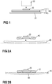
Figure 1 is a cross-sectional view of an arrangement for mounting semiconductor bodies onto a semiconductor substrate. -
Figure 2 , includingFigures 2A and 2B , illustrates cross-sectional views of a semiconductor substrate before and after mounting the semiconductor substrate onto a base plate. -
Figure 3 schematically illustrates a curved semiconductor substrate. -
Figure 4 schematically illustrates a semiconductor substrate that is mounted onto a base plate with an essentially homogenous connection layer. -
Figure 5 , includingFigures 5A to 5D , schematically illustrates an example of a method for processing a semiconductor substrate and an apparatus for processing a semiconductor substrate. -
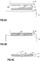
Figure 6 , includingFigures 6A to 6C , schematically illustrates a further example of a method for processing a semiconductor substrate. - In the following detailed description, reference is made to the accompanying drawings. The drawings show specific examples in which the invention may be practiced. It is to be understood that the features and principles described with respect to the various examples may be combined with each other, unless specifically noted otherwise. In the description as well as in the claims, designations of certain elements as "first element", "second element", "third element" etc. are not to be understood as enumerative. Instead, such designations serve solely to address different "elements". That is, e.g., the existence of a "third element" does not require the existence of a "first element" and a "second element". An electrical line or electrical connection as described herein may be a single electrically conductive element, or include at least two individual electrically conductive elements connected in series and/or parallel. Electrical lines and electrical connections may include metal and/or semiconductor material, and may be permanently electrically conductive (i.e., non-switchable). A semiconductor body as described herein may be made from (doped) semiconductor material and may be a semiconductor chip or be included in a semiconductor chip. A semiconductor body has electrically connecting pads and includes at least one semiconductor element with electrodes.
- Referring to
Figure 1 , asemiconductor substrate 10 is illustrated. Thesemiconductor substrate 10 includes adielectric insulation layer 11, a (structured)first metallization layer 111 attached to thedielectric insulation layer 11, and a second (structured)metallization layer 112 attached to thedielectric insulation layer 11. Thedielectric insulation layer 11 is disposed between the first andsecond metallization layers - Each of the first and
second metallization layers semiconductor substrate 10 may be a ceramic substrate, that is, a substrate in which thedielectric insulation layer 11 is a ceramic, e.g., a thin ceramic layer. The ceramic may consist of or include one of the following materials: aluminium oxide; aluminium nitride; zirconium oxide; silicon nitride; boron nitride; or any other dielectric ceramic. For example, thedielectric insulation layer 11 may consist of or include one of the following materials: Al2O3, AlN, or Si3N4. For instance, thesubstrate 10 may, e.g., be a Direct Copper Bonding (DCB) substrate, a Direct Aluminium Bonding (DAB) substrate, or an Active Metal Brazing (AMB) substrate. Thesubstrate 10 may also be a conventional printed circuit board (PCB) having a non-ceramicdielectric insulation layer 11. For instance, a non-ceramicdielectric insulation layer 11 may consist of or include a cured resin. - One or
more semiconductor bodies 20 may be arranged on thesemiconductor substrate 10. Each of thesemiconductor bodies 20 arranged on thesemiconductor substrate 10 may include an IGBT (Insulated-Gate Bipolar Transistor), a MOSFET (Metal-Oxide-Semiconductor Field-Effect Transistor), a JFET (Junction Field-Effect Transistor), a HEMT (High-Electron-Mobility Transistor), or any other suitable controllable semiconductor element. - The one or
more semiconductor bodies 20 may form a semiconductor arrangement on thesemiconductor substrate 10. InFigure 1 , only onesemiconductor body 20 is exemplarily illustrated. Thefirst metallization layer 111 ofFigure 1 is a continuous layer. Thefirst metallization layer 111, however, may be structured, for example if more than onesemiconductor body 20 is mounted to thesemiconductor substrate 10. "Structured metallization layer" means that thefirst metallization layer 111 is not a continuous layer, but includes recesses between different sections of the layer. Such recesses are schematically illustrated, for example, inFigure 6C , where thefirst metallization layer 111 includes three different sections.Different semiconductor bodies 20 may be mounted to the same or to different sections of thefirst metallization layer 111. Different sections of the first metallization layer may have no electrical connection or may be electrically connected to one or more other sections using, e.g.,bonding wires 21. An electrical connection (bonding wire 21) which electrically connects the semiconductor body on one section of thefirst metallization layer 111 with another section of thefirst metallization layer 111 is schematically illustrated inFigure 6C in a dashed line. The one ormore semiconductor bodies 20 may be electrically and mechanically connected to thesemiconductor substrate 10 by an electrically conductive connection layer (not illustrated inFigure 1 ). Such an electrically conductive connection layer may be a solder layer, a layer of an electrically conductive adhesive, or a layer of a sintered metal powder, e.g., a sintered silver powder, for example. - When mounting the one or
more semiconductor bodies 20 to thesubstrate 10, the substrate is usually placed on a contact surface of afirst mounting tool 31. Thesemiconductor bodies 20 are arranged on the substrate surface (top surface) and are then pressed onto thesubstrate 10 using asecond mounting tool 32. Appropriate methods for mounting asemiconductor body 20 to asemiconductor substrate 10 such as, e.g., soldering methods or sintering methods, are commonly known and will not be described in further detail. Thesubstrate 10, thesemiconductor bodies 20 as well as a contact layer (not illustrated) between thesubstrate 10 and thesemiconductor bodies 20 are usually heated during such mounting process, e.g., a sintering process. The temperature during the mounting of thesemiconductor bodies 20 may be more than 200° C, more than 300° C, or more than 400° C, for example. - When the
first metallization layer 111 and thesecond metallization layer 112 are exposed to pressure and/or heat, the layers are deformed. The deformation of thefirst metallization layer 111, however, may be different from the deformation of thesecond metallization layer 112. After the subsequent cooling of thesemiconductor substrate 10, this further leads to a deformation of thedielectric insulation layer 11 that is stacked between thefirst metallization layer 111 and thesecond metallization layer 112. Thus, thesubstrate 10 with thesemiconductor bodies 20 mounted thereon is permanently bended and usually has a convex deflection in the direction of thefirst metallization layer 111 on which thesemiconductor bodies 20 are mounted. This convex deflection or curvature is exemplarily illustrated inFigure 2A . The dashed lines inFigure 2A merely serve to illustrate the deflections of the different elements illustrated therein. The deflection of thesemiconductor substrate 10 or, in other words, the deviation from its original (essentially plane) form, may be, e.g., between about 100µm and about 500µm (difference in height between the edges and the center of the semiconductor substrate). - In a power semiconductor module, one or
more semiconductor substrates 10 are usually arranged on abase plate 40. Thebase plate 40 may have a thickness of between about 1mm and about 6mm, for example. Thebase plate 40, however, may also be thinner than 1mm or thicker than 6mm. Thebase plate 40 may consist of or include a metal or a metal matrix composite material (e.g., metal matrix composite MMC such as aluminium silicon carbide), for example. Suitable materials for ametal base plate 40 are, for example, copper, a copper alloy, aluminium, or an aluminium alloy. Thebase plate 40 may be coated by a thin coating layer (not illustrated). Such a coating layer may consist of or include nickel, silver, gold, or palladium, for example. The coating layer is optional and may improve the solderability of thebase plate 40. Thebase plate 40 may be arranged in a housing (not illustrated). The at least onesubstrate 10 may be electrically and mechanically connected to thebase plate 40 by afirst connection layer 50. Thefirst connection layer 50 may be a solder layer, a layer of an electrically conductive adhesive, or a layer of a sintered metal powder, e.g., a sintered silver powder, for example. Asemiconductor module 10 that is mounted on abase plate 40 is exemplarily illustrated inFigure 2B . Thebase plate 40 usually has a deflection. The deflection of thebase plate 40 is generally opposite to the deflection of thesemiconductor substrate 10. For example, if thesemiconductor substrate 10 has a convex deflection as has been described above, thebase plate 40 has a concave deflection in the direction of the surface on which the one ormore base plates 40 are mounted, as is illustrated inFigure 2 . The deflection of thebase plate 40 or, in other words, the deviation from its original (essentially plane) form, may be in the same order as the deflection of the semiconductor substrate, namely between about 100µm and about 500µm, for example (difference in height between the edges and the center of the base plate). - The examples illustrated herein describe a
semiconductor substrate 10 that is mounted on abase plate 40. This is, however only an example. In some power semiconductor module arrangements, thesemiconductor substrate 10 is not mounted to abase plate 40. Instead of to abase plate 40, thesemiconductor substrate 10 may be mounted to a heat sink (not illustrated), for example. A layer of heat-conducting paste may be arranged between thesemiconductor substrate 10 and the heat sink, for example. Mounting thesemiconductor substrate 10 to abase plate 40 or a heat sink are, however, only examples. Generally, thesemiconductor substrate 10 may be mounted to any suitable device or entity of a power semiconductor module arrangement. - The
semiconductor substrate 10 may be deflected in one direction in space only. However, as is schematically illustrated inFigure 3 , thesemiconductor substrate 10 may also be deflected in two directions in space, resulting in a cushion-shape or shell-like shape of thesubstrate 10. The same applies for thebase plate 40. - As can be seen from the arrangement illustrated in
Figure 2B , thefirst connection layer 50 may have a varying thickness. The thickness of thefirst connection layer 50 may be greater below the center of thesemiconductor substrate 10 and may be smaller near the edges of thesemiconductor substrate 10. In areas where thefirst connection layer 50 has a great thickness, the thermal resistance may be poor. The thinner thefirst connection layer 50, the lower the thermal resistance and the better the power density. The thickness of thefirst connection layer 50 may vary greatly for different power semiconductor modules. This is because the deflection of thesemiconductor substrate 10 and of thebase plate 40 currently cannot be reliably manipulated and may vary greatly between different substrates and base plates. A homogenousfirst connection layer 50, however, usually provides a better thermal resistance for the power semiconductor module which may lead to an increased reliability of the power semiconductor module. - Different methods are currently known for generating a homogenous
first connection layer 50 between thesemiconductor substrate 10 and the base plate 40 (or heat sink etc.). One method includes the positioning ofspacers 51 between thesemiconductor substrate 10 and thebase plate 40, as is schematically illustrated inFigure 4 . When mounting thesemiconductor substrate 10 to thebase plate 40, thesemiconductor substrate 10 is pressed onto thebase plate 40 or, more particularly, onto the one ormore spacers 51 with great force F10. For example, one or more weights may be placed on top of thesemiconductor substrate 10 to bend thesemiconductor substrate 10 in the direction of thebase plate 40 until it reaches thespacers 51. After the bending the semiconductor substrate may have essentially the same deflection as thebase plate 40. The weights may be in the range of several 100g, for example, and may apply a very selective force to only some areas of thesemiconductor substrate 10. The force, therefore, is not evenly distributed over the surface of thesemiconductor substrate 10. Placing rather heavy weights on thesemiconductor substrate 10, thereby bending thesemiconductor substrate 10 in the direction of thebase plate 40, leads to an essentially homogenousfirst connection layer 50. However, thesemiconductor substrate 10 and thesemiconductor bodies 20 mounted thereon are subjected to a great, selective force F10 and may be severely damaged during the mounting process. Furthermore, the heavy weights usually need to be handled manually, which may lead to physical harm of the operating personnel when many weights need to be handled. Another drawback lies in the fact that placing heavy weights (e.g., > 100g) on thesemiconductor substrate 10 alters the thermal capacity of the soldering forms that are used for mounting thesemiconductor substrates 10 to thebase plates 40 during a soldering process. - The present invention tries to avoid the exertion of a great force when mounting the
semiconductor substrate 10 onto thebase plate 40, thereby reducing the risk of damages of thesemiconductor substrate 10 and thesemiconductor bodies 20 mounted thereon. Further, the deflection of thesemiconductor substrates 10 may be more reliably adjusted such that it varies less betweendifferent semiconductor substrates 10. - As is schematically illustrated in
Figure 5A , an apparatus for processing asemiconductor substrate 10 includes afirst bending tool 33 and asecond bending tool 34. Thefirst bending tool 33 comprises a firstcurved surface 303, e.g., a curved top surface. Thesecond bending tool 34 comprises a secondcurved surface 304, e.g., a bottom surface. The firstcurved surface 303 may be a concave surface or a convex surface, for example. The deflection of the secondcurved surface 304 may be opposite to the deflection of the firstcurved surface 303. For example, the secondcurved surface 304 may be a convex surface if the first curved surface is a concave surface, and vice versa. Asemiconductor substrate 10 may be arranged between thefirst bending tool 33 and thesecond bending tool 34. For example, thesemiconductor substrate 10 may be placed on the firstcurved surface 303. According to one example, thesecond metallization layer 112 that is to be mounted to thebase plate 40, faces the firstcurved surface 303 and thefirst metallization layer 111 on which the one or more semiconductor bodies are to be mounted faces the secondcurved surface 304. - The first
curved surface 303 may be curved in only one direction of space to generate a deflection of thesemiconductor substrate 10 in only one direction. However, it is also possible that the firstcurved surface 303 is curved in two directions of space, e.g., pillow-shaped or shell-like shape, to generate a deflection of thesemiconductor substrate 10 in two directions as has been described with reference toFigure 3 before. The same applies for the secondcurved surface 304. - After placing the
semiconductor substrate 10 on thefirst bending tool 33, thesecond bending tool 34 may apply pressure (a force) to thesemiconductor substrate 10, as is schematically illustrated inFigure 5B . By applying a force to thesemiconductor substrate 10, thesemiconductor substrate 10 adapts to the shape of the first and thesecond bending tool semiconductor substrate 10, thesemiconductor substrate 10 may additionally be heated. For example, thesemiconductor substrate 10 may be heated to up to 200° C, to up to 300° C, to up to 400° C, or to up to 500° C. Heating thesemiconductor substrate 10, however, is optional. The process may also be performed at room temperature, for example. - The deflection of the
first bending tool 33 and thesecond bending tool 34 may be in the same dimension as the desired deflection of thesemiconductor substrate 10, for example. For example, thefirst bending tool 33 may have a deflection of, e.g., between about 100µm and about 500µm (difference in height between the edges/corners and the center of the first curved surface 303). Thesecond bending tool 34 may also have a deflection of, e.g., between about 100µm and about 500µm. The deflection of thefirst bending tool 33 may be in the same order as the deflection of thesecond bending tool 34, with the only difference that the orientation of the deflection is opposite to the orientation of the deflection of the first bending tool 33 (e.g.,first bending tool 33 concave,second bending tool 34 convex, or vice versa). In this way, an essentially homogenousfirst connection layer 50 may be obtained during a following soldering process during which thesemiconductor substrate 10 is mounted to thebase plate 40. Essentially homogenous in this context means that the thickness of thefirst connection layer 50 has a deviation of, e.g., maximally ± 25µm, maximally ± 50µm, or maximally ± 75µm of the average thickness over the entire area. According to another example, the thickness of thefirst connection layer 50 has a deviation of, e.g., maximally ± 13µm of the average thickness over the entire area. Other greater or smaller deviations are also possible. The deflection of thesemiconductor substrate 10, however, may also differ from the deflection of thebase plate 40, e.g., be greater or smaller than the deflection of thebase plate 40. In this way, afirst connection layer 50 may be obtained which has a greater thickness at the center of thesemiconductor substrate 10 and a smaller thickness near the edges/corners of thesemiconductor substrate 10. Or afirst connection layer 50 may be obtained which has a smaller thickness at the center of thesemiconductor substrate 10 and a greater thickness near the edges/corners of thesemiconductor substrate 10. For example, the thickness of thefirst connection layer 50 near the edges/corners (below the edges/corners) of thesemiconductor substrate 10 may be 50µm or more than 50µm thinner than the thickness at the center (below the center) of thesemiconductor substrate 10. Generally, typical average thicknesses of thefirst connection layer 50 may be between about 200µm and about 600µm. For some materials such as AlSiC, for example, a typical average thickness of down to about 50µm is also possible. - The thickness of the
first connection layer 50 may be reliably adjusted by pre-bending thesemiconductor substrate 10. By reliably adjusting the thickness of thefirst connection layer 50, the reliability of the semiconductor arrangement arranged on thesemiconductor substrate 10 as well as the reliability of the whole power semiconductor module arrangement may be increased. - In the Figures, the
second bending tool 34 has a surface area which is greater than the surface area of thesemiconductor substrate 10. This means that during the bending process, while thesecond bending tool 34 applies a pressure to thesemiconductor substrate 10, thesecond bending tool 34 completely covers thesemiconductor substrate 10. This is, however, only an example. Thesecond bending tool 34 may have a surface area which is smaller than the surface area of thesemiconductor substrate 10. This means that during the bending process, while thesecond bending tool 34 applies a pressure to thesemiconductor substrate 10, thesecond bending tool 34 does not completely cover thesemiconductor substrate 10. In this example, thesecond bending tool 34 only partly covers thesemiconductor substrate 10. For example, thesecond bending tool 34 may apply a pressure only on a central part of thesemiconductor substrate 10, while no pressure is applied near the edges of thesemiconductor substrate 10. - Further, the
second bending tool 34 that is illustrated in the Figures has a continuous surface. This is, however, only an example. Thesecond bending tool 34 may also include several parts (so-called multi-stamp tool). For example, a first part may apply a pressure to a central region of thesemiconductor substrate 10, a second part may apply a pressure to an edge region of thesemiconductor substrate 10, and a third part may apply a pressure to a region in between the central region and the edge region. There may be areas of thesemiconductor substrate 10, to which no pressure is applied directly. In other words, pressure may be applied selectively to different areas of thesemiconductor substrate 10. Using such a multi-stamp tool or asecond bending tool 34 with a surface area that is smaller than the surface area of thesemiconductor substrate 10, it is still possible to push thesemiconductor substrate 10 onto thefirst bending tool 33 such that it adapts to the shape of thefirst bending tool 33. - When the
second bending tool 34 is subsequently lifted from thesemiconductor substrate 10 and thesemiconductor substrate 10 is removed from thefirst bending tool 33, thesemiconductor substrate 10 is (permanently) bended (curved). Abended semiconductor substrate 10 is exemplarily illustrated inFigure 5C . In a following step, one ormore semiconductor bodies 20 may be mounted to thebended semiconductor substrate 10. Thesemiconductor bodies 20 may be soldered onto thesemiconductor substrate 10, for example. Soldering processes for mountingsemiconductor bodies 20 on asemiconductor substrate 10 are generally known and will not be described in further detail. - Once the
semiconductor bodies 20 are mounted to thesemiconductor substrate 10, thesemiconductor substrate 10 may be mounted to abase plate 40. As has been described above, one ormore spacers 51 may be arranged between thebase plate 40 and thesemiconductor substrate 10. The one or more spacers form an end stop for thesemiconductor substrate 10 during a soldering process. By pressing thesemiconductor substrate 10 against the one ormore spacers 51 during the soldering process such that thesemiconductor substrate 10 abuts thespacers 51, a homogenousfirst connection layer 50 between thesemiconductor substrate 10 and thebase plate 40 may be obtained. The height as well as the number ofspacers 51 defines the thickness of thefirst connection layer 50. Thespacers 51 may be separate elements that are mounted to thebase plate 40 by any appropriate means. According to another example, thespacers 51 are integral parts of thebase plate 40, e.g., protrusions or projections.Such spacers 51, however, are optional. - Generally, after pre-bending the semiconductor substrate with the
first bending tool 33 and thesecond bending tool 34, the deflection of thesemiconductor substrate 10 may essentially correspond to the deflection of thebase plate 40. As the deflection of thesemiconductor substrate 10 essentially corresponds to the deflection of thebase plate 40, it is no longer necessary to apply a great force to thesemiconductor substrate 10, as has been described with reference toFigure 4 before. It is no longer necessary to further bend thesemiconductor substrate 10 during the step of mounting thesemiconductor substrate 10 to thebase plate 40, because thesemiconductor substrate 10 is already pre-bended to have a concave deflection. The deflection of thesemiconductor substrate 10 essentially corresponds to the deflection of thebase plate 40 and, therefore, a comparatively small force F11 is necessary to press thesemiconductor substrate 10 to thebase plate 40. In order to apply a force F11 to thesemiconductor substrate 10, small weights may be placed on top of thesemiconductor substrate 10, to press thesemiconductor substrate 10 onto thebase plate 40. The small weights that are placed on thesemiconductor substrate 10 may be in the range of 10g or up to several 10g, for example. The weights that are placed on thesemiconductor substrate 10 are only needed to fixate thesemiconductor substrate 10 in place to keep the desired orientation of thesemiconductor substrate 10. -
Figure 6 schematically illustrates another method for processing asemiconductor substrate 10. When thesemiconductor bodies 20 are, e.g., sintered to thesemiconductor substrate 10 instead of soldered, it is possible to mount thesemiconductor bodies 20 to thesemiconductor substrate 10 while bending thesemiconductor substrate 10. Thesemiconductor substrate 10 may be placed on the firstcurved surface 303 of thefirst bending tool 33. Further, one ormore semiconductor bodies 20 may be arranged between thesemiconductor substrate 10 and thesecond bending tool 34. A layer of a metal powder, e.g., a silver powder, (not illustrated inFigure 6 ) may be arranged between thesemiconductor bodies 20 and thesemiconductor substrate 10, for example. Thesecond bending tool 34 may have a secondcurved surface 304, as has been described with respect toFigure 5 before. It is, however, also possible that thesecond bending tool 34 has a flat, or plane surface, as is schematically illustrated inFigure 6 . A layer ofcompensatory material 60 may be arranged between thesemiconductor substrate 10 with thesemiconductor bodies 20 and the second (curved or plane)surface 304. The layer ofcompensatory material 60 may be configured to distribute the force that is applied by thesecond bending tool 34 evenly over thesemiconductor substrate 10 and thesemiconductor bodies 20 arranged thereon. The layer ofcompensatory material 60 may consist of or comprise any material that is suitable to adjust any differences between the contours of the second (curved)surface 304 and thesemiconductor substrate 10, or, more precisely, between the contours of the second (curved)surface 304 and thesemiconductor substrate 10 in its desired form (its bended form). - A layer of
compensatory material 60 may generally also be used for the method that is described referring toFigure 5 above. Even if no semiconductor bodies are (yet) arranged on thesemiconductor substrate 10, the layer ofcompensatory material 60 may distribute the pressure that is applied by thesecond bending tool 34 evenly over thesemiconductor substrate 10. The layer ofcompensatory material 60 may be attached to thesecond surface 304, for example. According to another example, the layer ofcompensatory material 60 is a foil that is inserted between thesemiconductor substrate 10 and thesecond bending tool 34. - A flat (plane)
second surface 304, however, is only an example. It is also possible that thesecond bending tool 34 has a secondcurved surface 304, as has been described with respect toFigure 5 before. If thesecond bending tool 34 comprises a secondcurved surface 304, the layer ofcompensatory material 60 is optional and may be omitted. - Again referring to
Figure 6 , while applying a force (pressure) to thesemiconductor substrate 10 to pre-bend thesemiconductor substrate 10, thesemiconductor bodies 20 may, at the same time, be sintered to thesemiconductor substrate 10. Thesemiconductor substrate 10 may be heated during the sintering and bending process. For example, thesemiconductor substrate 10 may be heated to up to 200° C, to up to 300° C, to up to 400° C or to up to 500° C. Sinter processes are generally known and will not be described in further detail. - Generally speaking, a method for processing (pre-bending) a
semiconductor substrate 10 includes the step of arranging thesemiconductor substrate 10 on a firstcurved surface 303 of afirst bending tool 33. Pressure may be applied to thesemiconductor substrate 10 by using asecond bending tool 34 with asecond surface 304. Thesemiconductor substrate 10 is thereby pressed onto the firstcurved surface 303 and is thereby pre-bended. Thesecond surface 304 may be a flat surface or a curved surface. Ifsemiconductor bodies 20 are to be soldered to thesemiconductor substrate 10, a soldering process may follow after pre-bending thesemiconductor substrate 10. This means thatsemiconductor bodies 20 are soldered on thebended semiconductor substrate 10. Ifsemiconductor bodies 20 are to be sintered to thesemiconductor substrate 10, a sintering process may be performed while bending thesemiconductor substrate 10. A sintering process usually includes applying a certain pressure to thesemiconductor bodies 20 and may be performed at the same time while thesemiconductor substrate 10 is pre-bended. After bending thesemiconductor substrate 10, thesemiconductor substrate 10 is removed from thefirst bending tool 33. Thesemiconductor substrate 10 does not have a permanent connection to the first bending tool33 and is not permanently mounted to thefirst bending tool 33. After removing thesemiconductor substrate 10 from thefirst bending tool 33, thesemiconductor substrate 10 may be mounted to (e.g., soldered to) abase plate 40. Power semiconductor module arrangements often include a base plate 40 (with at least onesemiconductor substrate 10 mounted thereon) within a housing. Thefirst bending tool 33 and thesecond bending tool 34 are not components of such a power semiconductor module arrangement.
Claims (15)
- A method comprising:placing a semiconductor substrate (10) on a first curved surface (303) of a first bending tool (33);using a second bending tool (34) with a second surface (304) to apply pressure to the semiconductor substrate (10), thereby pressing the semiconductor substrate (10) onto the first curved surface (303) and bending the semiconductor substrate (10); andremoving the bended semiconductor substrate (10) from the first bending tool (33).
- The method of claim 1, wherein
the semiconductor substrate (10) comprises a dielectric insulation layer (11), a first metallization layer (111) and a second metallization layer (112), wherein the dielectric insulation layer (11) is disposed between the first and second metallization layers (111, 112); and
the semiconductor substrate (10) is placed on the first curved surface (303) such that the second metallization layer (112) faces the first curved surface (303). - The method of claim 2, further comprising:mounting at least one semiconductor body (20) to the first metallization layer (111) of the semiconductor substrate (10).
- The method of claim 3, wherein the at least one semiconductor body (20) is mounted to the first metallization layer (111) after bending the semiconductor substrate (10).
- The method of claim 4, wherein the at least one semiconductor body (20) is mounted to the first metallization layer (111) using a soldering process.
- The method of claim 3, wherein the at least one semiconductor body (20) is mounted to the first metallization layer (111) of the semiconductor substrate (10) during the step of bending the semiconductor substrate (10).
- The method of claim 6, wherein the at least one semiconductor body (20) is mounted to the first metallization layer (111) using a sintering process.
- The method of any of the preceding claims, further comprising:arranging a layer of compensatory material (60) between the semiconductor substrate (10) and the second surface (304), wherein the layer of compensatory material (60) is configured to distribute the pressure that is applied to the semiconductor substrate (10) by the second bending tool (34) evenly over the semiconductor substrate (10).
- The method of any of the preceding claims, wherein the step of applying pressure to the semiconductor substrate (10) is performed at room temperature or at a temperature of up to 200° C, up to 300° C, up to 400° C or up to 500° C.
- The method of any of the preceding claims, further comprising:mounting the bended semiconductor substrate (10) to a bended base plate (40) or a heat sink, wherein a first connection layer (50) is arranged between the semiconductor substrate (10) and the base plate (40) or heat sink.
- The method of claim 10, wherein, before mounting the semiconductor substrate (10) to the base plate (40) or heat sink,
a deflection of the bended semiconductor substrate (10) essentially corresponds to a deflection of the bended base plate (40) or heat sink, and the first connection layer (50) has an essentially even thickness;
a deflection of the bended semiconductor substrate (10) differs from a deflection of the bended base plate (40) or heat sink and the first connection layer (50) has a thickness which is greater below the center of the semiconductor substrate (10) and smaller near the edges of the semiconductor substrate (10); or
a deflection of the bended semiconductor substrate (10) differs from a deflection of the bended base plate (40) or heat sink and the first connection layer (50) has a thickness which is smaller below the center of the semiconductor substrate (10) and greater near the edges of the semiconductor substrate (10). - The method of claim 11, wherein the thickness of the first connection layer (50) has a deviation of maximally ± 75µm, maximally ± 50µm, maximally ± 25µm or of maximally ± 13µm from an average thickness over its entire area.
- The method of any of claims 10 to 12, wherein mounting the bended semiconductor substrate (10) to a bended base plate (40) or heat sink comprises:forming the first connection layer (50) on the bended base plate (40) or heat sink; andpressing the semiconductor substrate (10) onto the first connection layer (50).
- The method of claim 15, wherein pressing the semiconductor substrate (10) onto the first connection layer (50) comprises placing weights on the semiconductor substrate (10).
- An apparatus comprising:a first bending tool (33) with a first curved surface (303); anda second bending tool (34) with a second surface (304), wherein the second bending tool (34) is configured to apply pressure to a semiconductor substrate (10) that is arranged on the first curved surface (304), thereby pressing the semiconductor substrate (10) onto the first curved surface (303) and bending the semiconductor substrate (10).
Priority Applications (4)
| Application Number | Priority Date | Filing Date | Title |
|---|---|---|---|
| EP17178590.0A EP3422394B1 (en) | 2017-06-29 | 2017-06-29 | Method for processing a semiconductor substrate |
| US16/021,619 US10475668B2 (en) | 2017-06-29 | 2018-06-28 | Apparatus and method for processing a semiconductor substrate |
| CN201810712265.2A CN109216234B (en) | 2017-06-29 | 2018-06-29 | Apparatus and method for processing semiconductor substrate |
| US16/588,447 US10600658B2 (en) | 2017-06-29 | 2019-09-30 | Apparatus and method for bending a substrate |
Applications Claiming Priority (1)
| Application Number | Priority Date | Filing Date | Title |
|---|---|---|---|
| EP17178590.0A EP3422394B1 (en) | 2017-06-29 | 2017-06-29 | Method for processing a semiconductor substrate |
Publications (2)
| Publication Number | Publication Date |
|---|---|
| EP3422394A1 true EP3422394A1 (en) | 2019-01-02 |
| EP3422394B1 EP3422394B1 (en) | 2021-09-01 |
Family
ID=59269818
Family Applications (1)
| Application Number | Title | Priority Date | Filing Date |
|---|---|---|---|
| EP17178590.0A Active EP3422394B1 (en) | 2017-06-29 | 2017-06-29 | Method for processing a semiconductor substrate |
Country Status (3)
| Country | Link |
|---|---|
| US (2) | US10475668B2 (en) |
| EP (1) | EP3422394B1 (en) |
| CN (1) | CN109216234B (en) |
Families Citing this family (5)
| Publication number | Priority date | Publication date | Assignee | Title |
|---|---|---|---|---|
| DE102018110132B3 (en) * | 2018-04-26 | 2018-11-29 | Semikron Elektronik Gmbh & Co. Kg | Pressure sintering method in which power semiconductor devices are connected to a substrate via a sintered connection |
| EP4280271A1 (en) * | 2022-05-16 | 2023-11-22 | Infineon Technologies AG | Power semiconductor module arrangement and method for producing the same |
| US12599022B2 (en) * | 2022-07-22 | 2026-04-07 | Asmpt Singapore Pte. Ltd. | Apparatus for applying a sintering force via a compressible film |
| CN115401352B (en) * | 2022-08-18 | 2024-07-19 | 深圳基本半导体有限公司 | A welding method |
| CN115831890B (en) * | 2022-12-22 | 2023-12-22 | 黄山谷捷股份有限公司 | IGBT power module heat dissipation structure and processing technology thereof |
Citations (2)
| Publication number | Priority date | Publication date | Assignee | Title |
|---|---|---|---|---|
| US5379942A (en) * | 1992-10-01 | 1995-01-10 | Siemens Aktiengesellschaft | Method for producing a semiconductor modular structure |
| US20160254209A1 (en) * | 2013-10-10 | 2016-09-01 | Mitsubishi Materials Corporation | Power-module substrate with heat-sink and manufacturing method thereof |
Family Cites Families (10)
| Publication number | Priority date | Publication date | Assignee | Title |
|---|---|---|---|---|
| JP4183525B2 (en) * | 2003-02-14 | 2008-11-19 | シーケーディ株式会社 | Thin plate support device |
| JP2005109208A (en) * | 2003-09-30 | 2005-04-21 | Shin Etsu Handotai Co Ltd | Method of manufacturing light emitting element |
| GB0915473D0 (en) * | 2009-09-07 | 2009-10-07 | St Microelectronics Res & Dev | Improvements in or relating to CMOS sensors |
| US20120280368A1 (en) * | 2011-05-06 | 2012-11-08 | Sean Matthew Garner | Laminated structure for semiconductor devices |
| KR101991882B1 (en) * | 2011-05-13 | 2019-06-21 | 가부시키가이샤 사무코 | Method for manufacturing semiconductor epitaxial wafer, semiconductor epitaxial wafer, and method for manufacturing solid-state image pickup element |
| US8952532B2 (en) * | 2013-05-13 | 2015-02-10 | Intel Corporation | Integrated circuit package with spatially varied solder resist opening dimension |
| US10373995B2 (en) * | 2014-09-19 | 2019-08-06 | Microsoft Technology Licensing, Llc | Image sensor bending using tension |
| US9998643B2 (en) * | 2015-03-24 | 2018-06-12 | Semiconductor Components Industries, Llc | Methods of forming curved image sensors |
| US9870927B2 (en) * | 2015-04-02 | 2018-01-16 | Microsoft Technology Licensing, Llc | Free-edge semiconductor chip bending |
| US10062727B2 (en) * | 2016-09-09 | 2018-08-28 | Microsoft Technology Licensing, Llc | Strain relieving die for curved image sensors |
-
2017
- 2017-06-29 EP EP17178590.0A patent/EP3422394B1/en active Active
-
2018
- 2018-06-28 US US16/021,619 patent/US10475668B2/en active Active
- 2018-06-29 CN CN201810712265.2A patent/CN109216234B/en active Active
-
2019
- 2019-09-30 US US16/588,447 patent/US10600658B2/en active Active
Patent Citations (2)
| Publication number | Priority date | Publication date | Assignee | Title |
|---|---|---|---|---|
| US5379942A (en) * | 1992-10-01 | 1995-01-10 | Siemens Aktiengesellschaft | Method for producing a semiconductor modular structure |
| US20160254209A1 (en) * | 2013-10-10 | 2016-09-01 | Mitsubishi Materials Corporation | Power-module substrate with heat-sink and manufacturing method thereof |
Also Published As
| Publication number | Publication date |
|---|---|
| US10475668B2 (en) | 2019-11-12 |
| US10600658B2 (en) | 2020-03-24 |
| US20200027752A1 (en) | 2020-01-23 |
| CN109216234B (en) | 2022-01-21 |
| EP3422394B1 (en) | 2021-09-01 |
| CN109216234A (en) | 2019-01-15 |
| US20190006193A1 (en) | 2019-01-03 |
Similar Documents
| Publication | Publication Date | Title |
|---|---|---|
| US10600658B2 (en) | Apparatus and method for bending a substrate | |
| EP3340291B1 (en) | Method for producing an electronic module assembly and electronic module assembly | |
| US12009333B2 (en) | Semiconductor device | |
| JP3846699B2 (en) | Semiconductor power module and manufacturing method thereof | |
| CN115172290B (en) | Ceramic circuit substrates and semiconductor modules | |
| US12315821B2 (en) | Semiconductor device and method for manufacturing semiconductor device | |
| WO2017006916A1 (en) | Semiconductor device and method for manufacturing semiconductor device | |
| US11935811B2 (en) | Baseplate for a semiconductor module and method for producing a baseplate | |
| US20260101768A1 (en) | Base Plate for a Semiconductor Module Arrangement and Method for Producing a Base Plate | |
| WO2023152160A1 (en) | Power electronics module and method for its manufacture | |
| JP2013012693A (en) | Semiconductor module mounting method | |
| CN101304012B (en) | Semiconductor substrate with metal contact layer and corresponding production method | |
| US20230369175A1 (en) | Power semiconductor module arrangement and method for producing the same | |
| EP3627546B1 (en) | Power semiconductor module arrangement | |
| US20220157773A1 (en) | Pressure sintering device and method for manufacturing an electronic component | |
| EP3457434B1 (en) | Method for producing a semiconductor substrate for a power semiconductor module arrangement | |
| US20240055422A1 (en) | Method for manufacturing semiconductor module | |
| US20240055391A1 (en) | Method for manufacturing semiconductor module | |
| US20250275063A1 (en) | Method and system for connecting a terminal element to a substrate | |
| EP3889321B1 (en) | Method for producing a semiconductor substrate arrangement | |
| US20250233107A1 (en) | Semiconductor device and method of manufacturing the same | |
| CN118263139A (en) | Package with low warpage carrier | |
| EP3395783B1 (en) | Method for producing a sintered joint between a ceramic substrate and a carrier | |
| CN117936490A (en) | Semiconductor device and method of manufacturing such a semiconductor device |
Legal Events
| Date | Code | Title | Description |
|---|---|---|---|
| PUAI | Public reference made under article 153(3) epc to a published international application that has entered the european phase |
Free format text: ORIGINAL CODE: 0009012 |
|
| STAA | Information on the status of an ep patent application or granted ep patent |
Free format text: STATUS: REQUEST FOR EXAMINATION WAS MADE |
|
| 17P | Request for examination filed |
Effective date: 20180702 |
|
| AK | Designated contracting states |
Kind code of ref document: A1 Designated state(s): AL AT BE BG CH CY CZ DE DK EE ES FI FR GB GR HR HU IE IS IT LI LT LU LV MC MK MT NL NO PL PT RO RS SE SI SK SM TR |
|
| AX | Request for extension of the european patent |
Extension state: BA ME |
|
| STAA | Information on the status of an ep patent application or granted ep patent |
Free format text: STATUS: EXAMINATION IS IN PROGRESS |
|
| 17Q | First examination report despatched |
Effective date: 20191126 |
|
| RIC1 | Information provided on ipc code assigned before grant |
Ipc: H01L 23/373 20060101ALI20200709BHEP Ipc: H01L 21/48 20060101AFI20200709BHEP Ipc: H01L 21/67 20060101ALI20200709BHEP |
|
| GRAP | Despatch of communication of intention to grant a patent |
Free format text: ORIGINAL CODE: EPIDOSNIGR1 |
|
| STAA | Information on the status of an ep patent application or granted ep patent |
Free format text: STATUS: GRANT OF PATENT IS INTENDED |
|
| INTG | Intention to grant announced |
Effective date: 20210415 |
|
| GRAS | Grant fee paid |
Free format text: ORIGINAL CODE: EPIDOSNIGR3 |
|
| GRAA | (expected) grant |
Free format text: ORIGINAL CODE: 0009210 |
|
| STAA | Information on the status of an ep patent application or granted ep patent |
Free format text: STATUS: THE PATENT HAS BEEN GRANTED |
|
| AK | Designated contracting states |
Kind code of ref document: B1 Designated state(s): AL AT BE BG CH CY CZ DE DK EE ES FI FR GB GR HR HU IE IS IT LI LT LU LV MC MK MT NL NO PL PT RO RS SE SI SK SM TR |
|
| REG | Reference to a national code |
Ref country code: GB Ref legal event code: FG4D |
|
| REG | Reference to a national code |
Ref country code: CH Ref legal event code: EP Ref country code: AT Ref legal event code: REF Ref document number: 1427111 Country of ref document: AT Kind code of ref document: T Effective date: 20210915 |
|
| REG | Reference to a national code |
Ref country code: DE Ref legal event code: R096 Ref document number: 602017045030 Country of ref document: DE |
|
| REG | Reference to a national code |
Ref country code: IE Ref legal event code: FG4D |
|
| REG | Reference to a national code |
Ref country code: LT Ref legal event code: MG9D |
|
| REG | Reference to a national code |
Ref country code: NL Ref legal event code: MP Effective date: 20210901 |
|
| PG25 | Lapsed in a contracting state [announced via postgrant information from national office to epo] |
Ref country code: RS Free format text: LAPSE BECAUSE OF FAILURE TO SUBMIT A TRANSLATION OF THE DESCRIPTION OR TO PAY THE FEE WITHIN THE PRESCRIBED TIME-LIMIT Effective date: 20210901 Ref country code: SE Free format text: LAPSE BECAUSE OF FAILURE TO SUBMIT A TRANSLATION OF THE DESCRIPTION OR TO PAY THE FEE WITHIN THE PRESCRIBED TIME-LIMIT Effective date: 20210901 Ref country code: HR Free format text: LAPSE BECAUSE OF FAILURE TO SUBMIT A TRANSLATION OF THE DESCRIPTION OR TO PAY THE FEE WITHIN THE PRESCRIBED TIME-LIMIT Effective date: 20210901 Ref country code: ES Free format text: LAPSE BECAUSE OF FAILURE TO SUBMIT A TRANSLATION OF THE DESCRIPTION OR TO PAY THE FEE WITHIN THE PRESCRIBED TIME-LIMIT Effective date: 20210901 Ref country code: FI Free format text: LAPSE BECAUSE OF FAILURE TO SUBMIT A TRANSLATION OF THE DESCRIPTION OR TO PAY THE FEE WITHIN THE PRESCRIBED TIME-LIMIT Effective date: 20210901 Ref country code: NO Free format text: LAPSE BECAUSE OF FAILURE TO SUBMIT A TRANSLATION OF THE DESCRIPTION OR TO PAY THE FEE WITHIN THE PRESCRIBED TIME-LIMIT Effective date: 20211201 Ref country code: BG Free format text: LAPSE BECAUSE OF FAILURE TO SUBMIT A TRANSLATION OF THE DESCRIPTION OR TO PAY THE FEE WITHIN THE PRESCRIBED TIME-LIMIT Effective date: 20211201 Ref country code: LT Free format text: LAPSE BECAUSE OF FAILURE TO SUBMIT A TRANSLATION OF THE DESCRIPTION OR TO PAY THE FEE WITHIN THE PRESCRIBED TIME-LIMIT Effective date: 20210901 |
|
| REG | Reference to a national code |
Ref country code: AT Ref legal event code: MK05 Ref document number: 1427111 Country of ref document: AT Kind code of ref document: T Effective date: 20210901 |
|
| PG25 | Lapsed in a contracting state [announced via postgrant information from national office to epo] |
Ref country code: PL Free format text: LAPSE BECAUSE OF FAILURE TO SUBMIT A TRANSLATION OF THE DESCRIPTION OR TO PAY THE FEE WITHIN THE PRESCRIBED TIME-LIMIT Effective date: 20210901 Ref country code: LV Free format text: LAPSE BECAUSE OF FAILURE TO SUBMIT A TRANSLATION OF THE DESCRIPTION OR TO PAY THE FEE WITHIN THE PRESCRIBED TIME-LIMIT Effective date: 20210901 Ref country code: GR Free format text: LAPSE BECAUSE OF FAILURE TO SUBMIT A TRANSLATION OF THE DESCRIPTION OR TO PAY THE FEE WITHIN THE PRESCRIBED TIME-LIMIT Effective date: 20211202 |
|
| PG25 | Lapsed in a contracting state [announced via postgrant information from national office to epo] |
Ref country code: AT Free format text: LAPSE BECAUSE OF FAILURE TO SUBMIT A TRANSLATION OF THE DESCRIPTION OR TO PAY THE FEE WITHIN THE PRESCRIBED TIME-LIMIT Effective date: 20210901 |
|
| PG25 | Lapsed in a contracting state [announced via postgrant information from national office to epo] |
Ref country code: IS Free format text: LAPSE BECAUSE OF FAILURE TO SUBMIT A TRANSLATION OF THE DESCRIPTION OR TO PAY THE FEE WITHIN THE PRESCRIBED TIME-LIMIT Effective date: 20220101 Ref country code: SM Free format text: LAPSE BECAUSE OF FAILURE TO SUBMIT A TRANSLATION OF THE DESCRIPTION OR TO PAY THE FEE WITHIN THE PRESCRIBED TIME-LIMIT Effective date: 20210901 Ref country code: SK Free format text: LAPSE BECAUSE OF FAILURE TO SUBMIT A TRANSLATION OF THE DESCRIPTION OR TO PAY THE FEE WITHIN THE PRESCRIBED TIME-LIMIT Effective date: 20210901 Ref country code: RO Free format text: LAPSE BECAUSE OF FAILURE TO SUBMIT A TRANSLATION OF THE DESCRIPTION OR TO PAY THE FEE WITHIN THE PRESCRIBED TIME-LIMIT Effective date: 20210901 Ref country code: PT Free format text: LAPSE BECAUSE OF FAILURE TO SUBMIT A TRANSLATION OF THE DESCRIPTION OR TO PAY THE FEE WITHIN THE PRESCRIBED TIME-LIMIT Effective date: 20220103 Ref country code: NL Free format text: LAPSE BECAUSE OF FAILURE TO SUBMIT A TRANSLATION OF THE DESCRIPTION OR TO PAY THE FEE WITHIN THE PRESCRIBED TIME-LIMIT Effective date: 20210901 Ref country code: EE Free format text: LAPSE BECAUSE OF FAILURE TO SUBMIT A TRANSLATION OF THE DESCRIPTION OR TO PAY THE FEE WITHIN THE PRESCRIBED TIME-LIMIT Effective date: 20210901 Ref country code: CZ Free format text: LAPSE BECAUSE OF FAILURE TO SUBMIT A TRANSLATION OF THE DESCRIPTION OR TO PAY THE FEE WITHIN THE PRESCRIBED TIME-LIMIT Effective date: 20210901 Ref country code: AL Free format text: LAPSE BECAUSE OF FAILURE TO SUBMIT A TRANSLATION OF THE DESCRIPTION OR TO PAY THE FEE WITHIN THE PRESCRIBED TIME-LIMIT Effective date: 20210901 |
|
| REG | Reference to a national code |
Ref country code: DE Ref legal event code: R097 Ref document number: 602017045030 Country of ref document: DE |
|
| PLBE | No opposition filed within time limit |
Free format text: ORIGINAL CODE: 0009261 |
|
| STAA | Information on the status of an ep patent application or granted ep patent |
Free format text: STATUS: NO OPPOSITION FILED WITHIN TIME LIMIT |
|
| PG25 | Lapsed in a contracting state [announced via postgrant information from national office to epo] |
Ref country code: IT Free format text: LAPSE BECAUSE OF FAILURE TO SUBMIT A TRANSLATION OF THE DESCRIPTION OR TO PAY THE FEE WITHIN THE PRESCRIBED TIME-LIMIT Effective date: 20210901 Ref country code: DK Free format text: LAPSE BECAUSE OF FAILURE TO SUBMIT A TRANSLATION OF THE DESCRIPTION OR TO PAY THE FEE WITHIN THE PRESCRIBED TIME-LIMIT Effective date: 20210901 |
|
| 26N | No opposition filed |
Effective date: 20220602 |
|
| PG25 | Lapsed in a contracting state [announced via postgrant information from national office to epo] |
Ref country code: SI Free format text: LAPSE BECAUSE OF FAILURE TO SUBMIT A TRANSLATION OF THE DESCRIPTION OR TO PAY THE FEE WITHIN THE PRESCRIBED TIME-LIMIT Effective date: 20210901 |
|
| PG25 | Lapsed in a contracting state [announced via postgrant information from national office to epo] |
Ref country code: MC Free format text: LAPSE BECAUSE OF FAILURE TO SUBMIT A TRANSLATION OF THE DESCRIPTION OR TO PAY THE FEE WITHIN THE PRESCRIBED TIME-LIMIT Effective date: 20210901 |
|
| REG | Reference to a national code |
Ref country code: CH Ref legal event code: PL |
|
| REG | Reference to a national code |
Ref country code: BE Ref legal event code: MM Effective date: 20220630 |
|
| GBPC | Gb: european patent ceased through non-payment of renewal fee |
Effective date: 20220629 |
|
| PG25 | Lapsed in a contracting state [announced via postgrant information from national office to epo] |
Ref country code: LU Free format text: LAPSE BECAUSE OF NON-PAYMENT OF DUE FEES Effective date: 20220629 Ref country code: LI Free format text: LAPSE BECAUSE OF NON-PAYMENT OF DUE FEES Effective date: 20220630 Ref country code: IE Free format text: LAPSE BECAUSE OF NON-PAYMENT OF DUE FEES Effective date: 20220629 Ref country code: FR Free format text: LAPSE BECAUSE OF NON-PAYMENT OF DUE FEES Effective date: 20220630 Ref country code: CH Free format text: LAPSE BECAUSE OF NON-PAYMENT OF DUE FEES Effective date: 20220630 |
|
| PG25 | Lapsed in a contracting state [announced via postgrant information from national office to epo] |
Ref country code: GB Free format text: LAPSE BECAUSE OF NON-PAYMENT OF DUE FEES Effective date: 20220629 Ref country code: BE Free format text: LAPSE BECAUSE OF NON-PAYMENT OF DUE FEES Effective date: 20220630 |
|
| P01 | Opt-out of the competence of the unified patent court (upc) registered |
Effective date: 20230528 |
|
| PG25 | Lapsed in a contracting state [announced via postgrant information from national office to epo] |
Ref country code: HU Free format text: LAPSE BECAUSE OF FAILURE TO SUBMIT A TRANSLATION OF THE DESCRIPTION OR TO PAY THE FEE WITHIN THE PRESCRIBED TIME-LIMIT; INVALID AB INITIO Effective date: 20170629 |
|
| PG25 | Lapsed in a contracting state [announced via postgrant information from national office to epo] |
Ref country code: MK Free format text: LAPSE BECAUSE OF FAILURE TO SUBMIT A TRANSLATION OF THE DESCRIPTION OR TO PAY THE FEE WITHIN THE PRESCRIBED TIME-LIMIT Effective date: 20210901 Ref country code: CY Free format text: LAPSE BECAUSE OF FAILURE TO SUBMIT A TRANSLATION OF THE DESCRIPTION OR TO PAY THE FEE WITHIN THE PRESCRIBED TIME-LIMIT Effective date: 20210901 |
|
| PG25 | Lapsed in a contracting state [announced via postgrant information from national office to epo] |
Ref country code: TR Free format text: LAPSE BECAUSE OF FAILURE TO SUBMIT A TRANSLATION OF THE DESCRIPTION OR TO PAY THE FEE WITHIN THE PRESCRIBED TIME-LIMIT Effective date: 20210901 |
|
| PG25 | Lapsed in a contracting state [announced via postgrant information from national office to epo] |
Ref country code: MT Free format text: LAPSE BECAUSE OF FAILURE TO SUBMIT A TRANSLATION OF THE DESCRIPTION OR TO PAY THE FEE WITHIN THE PRESCRIBED TIME-LIMIT Effective date: 20210901 |
|
| PGFP | Annual fee paid to national office [announced via postgrant information from national office to epo] |
Ref country code: DE Payment date: 20250822 Year of fee payment: 9 |
|
| REG | Reference to a national code |
Ref country code: DE Ref legal event code: R079 Ref document number: 602017045030 Country of ref document: DE Free format text: PREVIOUS MAIN CLASS: H01L0021480000 Ipc: H10W0076010000 |