EP3420783B1 - Driver apparatus - Google Patents
Driver apparatus Download PDFInfo
- Publication number
- EP3420783B1 EP3420783B1 EP17711738.9A EP17711738A EP3420783B1 EP 3420783 B1 EP3420783 B1 EP 3420783B1 EP 17711738 A EP17711738 A EP 17711738A EP 3420783 B1 EP3420783 B1 EP 3420783B1
- Authority
- EP
- European Patent Office
- Prior art keywords
- light emitting
- voltage
- led
- signal
- circuitry
- Prior art date
- Legal status (The legal status is an assumption and is not a legal conclusion. Google has not performed a legal analysis and makes no representation as to the accuracy of the status listed.)
- Active
Links
Images


Classifications
-
- H—ELECTRICITY
- H05—ELECTRIC TECHNIQUES NOT OTHERWISE PROVIDED FOR
- H05B—ELECTRIC HEATING; ELECTRIC LIGHT SOURCES NOT OTHERWISE PROVIDED FOR; CIRCUIT ARRANGEMENTS FOR ELECTRIC LIGHT SOURCES, IN GENERAL
- H05B45/00—Circuit arrangements for operating light-emitting diodes [LED]
- H05B45/30—Driver circuits
- H05B45/395—Linear regulators
-
- H—ELECTRICITY
- H04—ELECTRIC COMMUNICATION TECHNIQUE
- H04B—TRANSMISSION
- H04B10/00—Transmission systems employing electromagnetic waves other than radio-waves, e.g. infrared, visible or ultraviolet light, or employing corpuscular radiation, e.g. quantum communication
- H04B10/11—Arrangements specific to free-space transmission, i.e. transmission through air or vacuum
- H04B10/114—Indoor or close-range type systems
- H04B10/116—Visible light communication
-
- H—ELECTRICITY
- H05—ELECTRIC TECHNIQUES NOT OTHERWISE PROVIDED FOR
- H05B—ELECTRIC HEATING; ELECTRIC LIGHT SOURCES NOT OTHERWISE PROVIDED FOR; CIRCUIT ARRANGEMENTS FOR ELECTRIC LIGHT SOURCES, IN GENERAL
- H05B45/00—Circuit arrangements for operating light-emitting diodes [LED]
- H05B45/30—Driver circuits
- H05B45/34—Voltage stabilisation; Maintaining constant voltage
-
- H—ELECTRICITY
- H05—ELECTRIC TECHNIQUES NOT OTHERWISE PROVIDED FOR
- H05B—ELECTRIC HEATING; ELECTRIC LIGHT SOURCES NOT OTHERWISE PROVIDED FOR; CIRCUIT ARRANGEMENTS FOR ELECTRIC LIGHT SOURCES, IN GENERAL
- H05B47/00—Circuit arrangements for operating light sources in general, i.e. where the type of light source is not relevant
- H05B47/10—Controlling the light source
- H05B47/105—Controlling the light source in response to determined parameters
- H05B47/14—Controlling the light source in response to determined parameters by determining electrical parameters of the light source
-
- H—ELECTRICITY
- H05—ELECTRIC TECHNIQUES NOT OTHERWISE PROVIDED FOR
- H05B—ELECTRIC HEATING; ELECTRIC LIGHT SOURCES NOT OTHERWISE PROVIDED FOR; CIRCUIT ARRANGEMENTS FOR ELECTRIC LIGHT SOURCES, IN GENERAL
- H05B47/00—Circuit arrangements for operating light sources in general, i.e. where the type of light source is not relevant
- H05B47/10—Controlling the light source
- H05B47/165—Controlling the light source following a pre-assigned programmed sequence; Logic control [LC]
-
- H—ELECTRICITY
- H05—ELECTRIC TECHNIQUES NOT OTHERWISE PROVIDED FOR
- H05B—ELECTRIC HEATING; ELECTRIC LIGHT SOURCES NOT OTHERWISE PROVIDED FOR; CIRCUIT ARRANGEMENTS FOR ELECTRIC LIGHT SOURCES, IN GENERAL
- H05B47/00—Circuit arrangements for operating light sources in general, i.e. where the type of light source is not relevant
- H05B47/10—Controlling the light source
- H05B47/175—Controlling the light source by remote control
- H05B47/19—Controlling the light source by remote control via wireless transmission
-
- H—ELECTRICITY
- H05—ELECTRIC TECHNIQUES NOT OTHERWISE PROVIDED FOR
- H05B—ELECTRIC HEATING; ELECTRIC LIGHT SOURCES NOT OTHERWISE PROVIDED FOR; CIRCUIT ARRANGEMENTS FOR ELECTRIC LIGHT SOURCES, IN GENERAL
- H05B45/00—Circuit arrangements for operating light-emitting diodes [LED]
- H05B45/10—Controlling the intensity of the light
-
- Y—GENERAL TAGGING OF NEW TECHNOLOGICAL DEVELOPMENTS; GENERAL TAGGING OF CROSS-SECTIONAL TECHNOLOGIES SPANNING OVER SEVERAL SECTIONS OF THE IPC; TECHNICAL SUBJECTS COVERED BY FORMER USPC CROSS-REFERENCE ART COLLECTIONS [XRACs] AND DIGESTS
- Y02—TECHNOLOGIES OR APPLICATIONS FOR MITIGATION OR ADAPTATION AGAINST CLIMATE CHANGE
- Y02B—CLIMATE CHANGE MITIGATION TECHNOLOGIES RELATED TO BUILDINGS, e.g. HOUSING, HOUSE APPLIANCES OR RELATED END-USER APPLICATIONS
- Y02B20/00—Energy efficient lighting technologies, e.g. halogen lamps or gas discharge lamps
- Y02B20/30—Semiconductor lamps, e.g. solid state lamps [SSL] light emitting diodes [LED] or organic LED [OLED]
Definitions
- the present invention relates to driver apparatus, for instance a universal luminaire driver.
- LEDs light-emitting diodes
- Each type of LED has a set of operating conditions defined, for example, by the minimum and maximum values of voltage and current for which the LED will operate correctly.
- Each type of LED also has a set of intrinsic performance characteristics, for example, an achievable light intensity of light produced by the LED. This is relevant when used in the context of optical light communication.
- Other intrinsic performance characteristics of LEDs are also relevant in such a context.
- LEDs have an intrinsic modulation frequency bandwidth dependent on the method of manufacture and the materials the LED is made of.
- OLEDs Organic Light Emitting Diodes
- solid-state LEDs typically have higher modulation bandwidth in the region of several megahertz.
- Luminaires for optical light communication are designed to serve a specific purpose.
- the design of a driver circuit of the luminaire may be tailored to incorporate a specific type and/or number of LEDs.
- the driving circuit may be tailored to the operating conditions of the LED to provide good performance.
- the driving circuit can also be tailored to one or more LEDs to provide improved performance compared to the individual intrinsic performance characteristics of the individual LED.
- a bespoke driving circuit tailored to a specific type of LED may not be suitable for use with a different type of LED.
- Reasons for unsuitability include the bespoke driving circuit being set to provide a voltage and/or current that is insufficient for the chosen type of LED, in effect leading to a reduced quality optical signal.
- the performance of other components in the driving circuit are also dependent on the type of LED connected to the driving circuit and using an LED type other than the type for which the driving circuit was tailored can lead to inefficiency in the operation of the LED and the other component parts.
- a component of a driving circuit is a transistor
- the use of an LED that requires different voltage levels to operate in the same current signal range may cause the transistor to dissipate unnecessarily high thermal energy levels leading to inefficiency in the driving circuit.
- Transistors are also built with a finite tolerance to voltage drop before the transistor is destroyed. Therefore, connecting a different type of LED carries the risk of destroying the transistor.
- LEDs As is known, visible light communication uses intensity modulation of LEDs.
- An intrinsic property of LEDs is their response to an input current, which varies from LED to LED and can be characterised using a frequency modulation bandwidth.
- a different type of LED connected to a tailored LED driver may not be able to provide a sufficient quality of signal, as measured by a signal to noise ratio, over the full modulation bandwidth originally intended.
- WO 2011/141768 describes a ballast used to drive high intensity discharge lamps and, more particularly to the same HID ballast being used for a bank of interconnected light emitting diodes (LEDs).
- US 2010/320922 describes an illumination device including light-emitting diodes.
- a luminaire driver apparatus for use with one or more light emitting diodes or other light sources, comprising: voltage control circuitry configured to regulate a supply voltage to one or more light emitting diodes or other light sources; driving circuitry configured to provide a drive current to the one or more light emitting diodes or other light sources, the drive current being dependent on the supply voltage, wherein the driving circuitry is configured to modulate the drive current based on a modulated drive signal such that the one or more light emitting diodes or other light sources produces an optical signal, wherein at least one of the driving circuitry and control circuitry are operable to adapt to a plurality of different types of light emitting diode or other light source.
- the plurality of different types of light emitting diode or other light sources may comprise light emitting diodes or other light sources that have at least one of different minimum and/or maximum operating current and/or voltage levels, different modulation frequency bandwidths, different optical response to input current.
- the modulated drive signal may be such as to modulate the optical signal to represent data for example data of an input information signal.
- the control circuitry may comprise monitoring means configured to monitor a parameter of the driving circuit wherein the parameter is representative of the operation of the light emitting diode or other light source.
- the control circuitry may be further configured to automatically adjust the supply voltage to the one or more light emitting diodes or other light sources based on the monitored parameter.
- the modulated drive signal may comprise a range of values and the automatic adjustment of the supply voltage may permit operation of the light emitting diode over said range of values.
- the supply voltage may be selected to permit operation of the light emitting diode in a linear region of an optical power output to current input curve of the light emitting diode.
- the automatic adjustment of the voltage supply to the light emitting diode or other light source may maintain the monitored parameter at a predetermined value or within a predetermined range or at a minimum value, optionally thereby to reduce power consumption of components of the driving circuitry.
- the automatic adjustment of the voltage supply to the light emitting diode may maintain the monitored parameter at an extreme value to reduce power consumption of components of the driving circuitry.
- the driving circuitry may comprise a transistor or other current and/or voltage regulating component, configured to control the drive current using the drive signal and the monitored parameter of the driving circuitry may be representative of or dependent on an input or output voltage of the transistor or other current and/or voltage regulating component.
- the monitored parameter may be maintained at the predetermined value or within the predetermined range or at the minimum value thereby to reduce voltage drop across the transistor or other current and/or voltage regulating component.
- the driving circuitry of the luminaire may comprise compensating means configured to at least partially reduce distortion to the optical signal produced by the one or more light emitting diodes or other light sources.
- the compensating means may be further configured to at least partially reduce a contribution to the distortion to the optical signal from a response of the one or more light emitting diodes or other light sources to the drive signal.
- the optical signal may be conveyed through a free-space communication channel to a receiver and the compensating means may be further configured to at least partially reduce a contribution to the distortion to the optical signal from the free-space communication channel.
- the distortion of the optical signal can be represented by a deformation in a shape of the optical signal and the compensating means is configured to manipulate the drive signal to at least partially reduce said deformation to the shape of the optical signal.
- the compensating means of the luminaire may comprise at least one of pre-distortion circuitry, pre-equalisation circuitry or pre-coding circuitry.
- the compensating means may be configured to carry out adaptive bit and energy loading.
- the compensating means may comprise one or more digital and/or analogue filters.
- the coefficients representing the filters may be pre-determined.
- the coefficients may be adapted to the received signal using channel state information.
- the pre-coding (e.g. pre-distortion) step may be a transformation on the or an information signal which reduces the peakiness of the signal distribution and, hence, reduces the peak-to-average power ratio (PAPR) of the information signal. It may also be a processing step which inverts a non-linear input-output characteristic of an LED or other light source in order to reduce the non-linear distortion which leads to performance degradation.
- the compensating means may apply any suitable pre-coding/pre-distortion techniques.
- the compensating means may be configured to operate in a frequency domain or a time domain
- the types of light emitting diode used with the luminaire may for example have an intrinsic optical modulation bandwidth below 1 MHz, or below 2 MHz, or below 10 MHz.
- the types of LED may be one of phosphor converted LED, multi-chip LED, micro LED and resonant cavity LED.
- the light and/or optical signals may comprise electromagnetic waves with wavelengths in the range 1 nm to 2500 nm.
- the light and/or optical signals may comprise ultraviolet, visible light, near-infrared light or THz radiation.
- the luminaire driver apparatus may be configured for optical wireless communication and/or may form part of an optical wireless communication system.
- the drive signal may be modulated using at least one of a single carrier modulation scheme, a multi-carrier modulation scheme and a carrier-less modulation scheme.
- apparatus comprising at least one light source, a luminaire driver apparatus as claimed or described herein, and a power source providing a supply voltage and/or drive current.
- There may be provided a method of operating at least one light source comprising installing at least one light source in a luminaire driver apparatus as claimed or described herein, and operating at least one of the driving circuitry and control circuitry to adapt to the light source.
- FIG. 1 shows a schematic block diagram illustrating the principles of optical wireless communication.
- a transmitter 10 is configured to send an optical signal in which information is encoded through an optical communication channel 11 to a receiver 12.
- the optical communication channel 11 may be a free-space communication channel.
- a driving circuit to drive an LED to produce the optical signal containing encoded information is also provided, together with a photo-diode to receive the optical signal and circuitry/processor to process the received signal.
- the physical limitation of the LED due to its frequency response to a drive current is a significant contribution to distortion of an optical signal (e.g. a reduction in the signal to noise ratio of an optical signal) in an optical light communication channel formed between a transmitter and a receiver.
- Frequency response of the channel itself can also be measured.
- a non-flat communication channel between the transmitter and receiver may, for example, be caused by multiple copies of the same optical signal arriving at different points in time at the receiver.
- the LED is characterised by a modulation frequency response in the frequency domain (and equivalently by an impulse response in the time domain).
- Gain at a given modulation frequency can be defined as the ratio of optical power at that frequency to optical power at a reference modulation frequency.
- the reference modulation frequency may be chosen such that the optical power at the reference modulation frequency is a maximum value and/or such that the reference modulation frequency is zero.
- Above a certain modulation frequency the gain of the LED will be less than a certain threshold. Typically this threshold is chosen to be negative 3dB.
- a gain of more than negative 3dB corresponds to an attenuation of less that positive 3dB.
- a gain at an upper bandwidth modulation frequency of negative 3dB corresponds to a halving of the optical signal variance at the upper bandwidth modulation frequency. This value typically depends on the injected carrier lifetime of the LED and the parasitic capacitance of the LED.
- FIG. 2 shows a high level block diagram of a Universal Luminaire Driver for optical communication.
- the luminaire 13 has control circuitry 14 and driving circuitry 15.
- the driving circuitry 15 has two modules: a light emitting diode circuit module 16 and a signal circuit module 18.
- the light emitting diode circuit module 16 is adapted such that one or more light emitting diodes can be connected to the luminaire.
- An interface 20 is provided between the light emitting diode circuit module 16 and the signal circuit module 18.
- the luminaire 13 can be used with one or more light emitting diodes of different types.
- the luminaire 13 is connected to a power source 22 by a power connection 24 and to a network infrastructure 26 through a network connection 28.
- the power source 22 can be a standard power supply unit.
- the power source 22 can provide different voltage levels to luminaire 13 through the power connection 24. Each of the different voltage levels can be present in one or more wires of the power connection 24.
- the different voltage levels provided may be referred to as voltage rails. Different components of the luminaire 13 may use different voltage levels in accordance with the requirements of the component.
- a first voltage rail at a first voltage level may be provided to the light emitting diode circuit module 16 and a second voltage rail at a second voltage level may be provided to the signal circuit module 18.
- the light emitting diode circuit module 16 must provide a sufficient voltage level to power a connected light emitting diode and is therefore likely to require a different voltage level than component parts of the signal circuit module 18.
- the control circuitry 14 is connected to the light emitting diode circuit module 16 and to the voltage rail provided to the light emitting diode circuit module 16.
- the control circuitry 14 is configured to control the voltage rail provided to the light emitting diode circuit module 16. The operation of the control circuitry 14 is explained in more detail with reference to Figure 3 and Figure 4 .
- the signal circuit module 18 is configured to provide a drive signal to the light emitting diode circuit module 16, thereby allowing an optical signal to be produced. By manipulating the drive current, the signal circuit module 18 can compensate, and at least partially reduce any distortion in the optical signal originating from the light emitting diode circuit module 16 or from a free-space communication channel. Distortion may be present because the connected LED is not capable of achieving modulation frequencies required.
- the signal circuit module 18 is described in more detail with reference to Figure 5, Figure 6 and Figure 7 .
- FIG. 3 shows an illustrative embodiment of driving circuitry and control circuitry.
- the driving circuitry has a LED circuit line 30 connected to a voltage supply line 32, and additional signal circuitry 34.
- the control circuitry is represented by a control circuit 36 connected between the LED circuit line 30 and the voltage supply line 32.
- the LED circuit line 30 extends between, and is connected to, the voltage supply line 32 at a first end and an earth ground 38 at a second end. Traversing the LED circuit line 30 in the direction from the voltage supply end to the earth ground end, the LED circuit line 30 has the following connected components: a first LED 40, a second LED 42, a control circuit connection 44, a transistor 46 and a resistor 48.
- the control circuit connection 44 provides a connection between the control circuit 36 and the LED circuit line 30.
- the apparatus may be configured for installation of any suitable number of LEDs, for example a single LED or any other suitable number of LEDs, and embodiments are not limited to the two LED arrangement shown in Figure 3 .
- the LEDs may be arranged in series or in parallel.
- the transistor 46 provides an interface between the LED circuit line 30 and the additional signal circuitry 34.
- the transistor 46 shown is a single metal-oxide semiconductor field-effect-transistor (MOSFET). However, different transistor technology can be used.
- the transistor 46 has three terminals: a gate terminal, a drain terminal and a source terminal.
- the transistor 46 is configured in the circuit such that the signal circuitry 34 is connected to the gate terminal to provide a drive signal 50 to the transistor 46.
- the gate and source terminals are connected across the LED circuit line 30 such that the connection between the drain and source terminals in the transistor 46 forms part of the LED circuit line 30.
- the transistor 46 is oriented such that the drain terminal is on the voltage supply line 32 side of the LED circuit line 30 and the source terminal is on the earth ground 38 side of the LED circuit line 30.
- Figure 3 shows a first control circuit line 52 that connects at a first end to the LED circuit line 30 and at a second end to a second earth ground point 54.
- the connection at the first end of the first control circuit line 52 is the control circuit connection 44 of the LED circuit line 30.
- Traversing the first control circuit line 52 from the control circuit connection 44 to the second earth ground point 54 the following components are connected: a control circuit resistor 56, a control circuit junction 58 and a control circuit capacitor 60. Together the control circuit capacitor 60 and the control circuit resistor 56 provide a simple RC filter for a signal in the first control circuit line 52.
- a second control circuit line 62 connects the first control circuit line 52 to the voltage supply line 32.
- the second control circuit line 62 connects to the first control circuit line 52 at the control circuit junction 58 which is located between the control circuit resistor 56 and the control circuit capacitor 60. Connected on the second control circuit line 62 is a voltage control circuit 64 which is described with reference to Figure 4 .
- the signal circuitry 34 is configured to provide the drive signal 50 to the gate of transistor 46 to control the current in the LED circuit line 30. Control of the current includes controlling the magnitude of the current.
- the drive signal 50 has a voltage value of V in .
- the drive signal 50 is modulated and contains a DC component and an AC component.
- the DC component sets the operating point of the device (the DC bias of the drive current through the LED).
- the AC component corresponds to the modulation of the signal and varies the current provided to the LEDs. Generation of the drive signal is discussed in more detail with reference to Figures 5 to 7 .
- a non-zero value of the voltage rail provides a voltage difference between the voltage supply line 32 and earth ground 38. If the voltage difference over each one of the LEDs is high enough, the voltage difference allows a drive current to flow through the LED circuit line 30.
- the drive current flows through the resistor 48 which has a resistance (R).
- the resistor 48 can be chosen to stabilize the drive current flowing through the LEDs.
- the transistor 46 operates to control this current flow and can be considered as providing a voltage controlled current source. When a gate voltage is supplied to the transistor 46 with a voltage that is higher than the value of the source voltage then the transistor 46 acts like a variable resistor between the drain and source terminals. In this case, the resistance between the drain and source terminals varies with the voltage difference between the gate and source terminals.
- the resistance provided by the transistor on the LED circuit line 30 also varies. For a given value of the gate voltage there is a corresponding value of the drive current in the LED circuit line 30. This current flows and is delivered to the first LED 40 and the second LED 42.
- the voltage at different points of the LED circuit line 30 have different values.
- the values of the voltage over the resistor 48, the voltage over the LEDs and the voltage over the transistor 46 are the values of the voltage over the resistor 48, the voltage over the LEDs and the voltage over the transistor 46.
- V R I LED R.
- the voltage over each LED will correspond to an intrinsic voltage-current characteristic of each LED.
- the relationship between voltage and current for each LED can be represented as a function which may be approximately an exponential function: e.g. current is approximately an exponential function of voltage. A small change to the voltage across the LED can therefore result in a large change in current through the LED.
- each LED has an intrinsic threshold characteristic. This can be represented in a current-voltage function as a threshold point corresponding to a threshold voltage value. A voltage across the LED below the threshold voltage value will correspond to no current flowing through the LED and hence a LED will not produce any light at this voltage value.
- the voltage over the transistor 46 typically requires a low positive value to allow a current to flow through transistor 46.
- a relationship between power or intensity of a generated optical output of an LED and current input to the LED can be represented as a function or as an optical output to current input curve.
- the luminaire may be configured such that operation is in a linear region of this curve.
- the voltage over the transistor (between the source and drain terminals) is equal to the difference of the voltage at the drain terminal and the value of the voltage at the source terminal.
- the gate voltage regulates the current through the transistor 46. Therefore the value of V monitor does not have an influence on the value of the current in the LED circuit line 30. In practice, V monitor has a negligible effect as the MOSFET acts as a current source with very high output impedance.
- the value of V monitor is also alternating and has a characterising frequency.
- the control circuit resistor 56 and the control circuit capacitor 60 are connected in series along the first control circuit line 52 and act together as a simple RC filter for V monitor .
- the voltage can be considered as split between the control circuit resistor 56 and the control circuit capacitor 60, where the voltage over the control circuit capacitor 60 is input to the voltage control circuit 64.
- This configuration provides a low-pass filter for V monitor from the LED circuit line 30. High frequency signals are attenuated e.g. shorted to second earth ground point 54 by the capacitor and low frequency signals are passed.
- the RC filter therefore acts to provide a low frequency (average DC) voltage of the transistor drain to the voltage control circuit 64.
- the cut-off frequency of the RC filter, above which no signals pass, will depend on the filter design and choice of components e.g. capacitance and resistance of the components.
- FIG. 4 is a block diagram showing an example implementation of the voltage control circuit 64.
- the voltage control circuit 64 is a DC supply circuit.
- the example implementation shown is a digital embodiment but this is just one possibility for realizing the voltage control circuitry.
- the voltage control circuitry takes an input signal 66 and returns an output signal 68.
- the voltage control circuitry has several component parts: an analogue-to-digital converter 70, a digital control logic component 72, and a digitally-controlled DC to AC converter 74.
- the input signal 66 is an analogue signal and is converted to a digital signal 76 by the analogue-to-digital converter 70.
- the digital signal 76 then passes to the digital control logic component 72.
- the digital control logic component 72 assesses the digital signal 76 and produces digital instructions 78.
- the digital instructions 78 are then converted to the output signal 68 by the digitally-controlled DC to AC converter 74.
- the input signal 66 corresponds to a filtered or averaged voltage from the control circuit connection 44 and the output signal 68 sets the rail voltage of the voltage supply line 32.
- a modulated drive signal 50 is provided to the transistor 46 which acts as a voltage controlled current source.
- the modulated drive signal 50 controls the drive current in the LED circuit line 30 provided to the connected LED through the transistor 46.
- a value based on V monitor is recorded by the control circuit 36. Variation in the drive current causes a variation in V monitor. V monitor is also dependent on the value of the voltage of the voltage supply line 32.
- An analogue input signal is provided to the voltage control circuit 64 based on an average value of V monitor that is determined by a filtering of V monitor.
- the digital control logic component 72 is configured to determine a minimum value of the V monitor that corresponds to fully operational conditions of the attached LED. That minimum value is encoded into a set of digital instructions 78 that is then converted to the analogue output signal 68 that sets the voltage of the voltage supply line 32. The process will automatically set the correct voltage for the attached type or types of LED and thereby regulates the voltage supplied to the one or more LEDs.
- the voltage control circuit 64 is configured to automatically adjust the voltage of the voltage supply line 32 to increase voltage above threshold.
- V monitor will register a high value.
- the voltage control circuit 64 is configured to automatically adjust the voltage of the voltage supply line 32 to decrease the voltage to below a level that is dangerous to the transistor.
- the adjustment made by the voltage control circuit 64 may be based on iterative steps of registering a value for V monitor and updating the voltage supply line 32 voltage based on V monitor.
- a continuous monitoring of V monitor can be provided during real time operation of the luminaire. This is particularly advantageous as operational characteristics of the LED and other components in the luminaire that have an effect on V monitor can be dependent on environmental factors, for example temperature changes. Continuous and automatic adjustment of V monitor allows the luminaire to adjust to temperature changes in the environment.
- the drive signal 50 of the signal circuitry 34 controls the drive current provided to the LEDs.
- Different types of LED connected to the LED circuit line 30 will respond differently to the drive current.
- a new type of LED connected to the luminaire may be able to operate in accordance to its voltage and current requirements due to the control circuit.
- the drive signal itself may contain portions at modulation frequencies that are beyond the physical capabilities of the LED i.e. the LED cannot broadcast an optical signal over the full range of modulation frequencies required without significant reduction in the signal to noise ratio of the information signal received at the receiver.
- the luminaire may be capable of compensating for any physical distortion in the communication channel between the transmitter and the receiver caused by the LED.
- Compensating means is included in the driving circuitry to modify the drive signal.
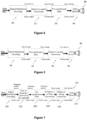
- Figure 5 is a block diagram of an embodiment of signal generating circuitry comprising: a digital modulation encoding module 90, a pre-equalisation filter 92, a digital-to-analogue converter 94, a LED driver circuit 96 and an LED 98.
- An input information signal comprises data in the form of bits.
- the information signal may originate from a processor or external network.
- This information signal is modulated into a digital signal using any suitable modulation scheme by the digital modulation encoding module 90.
- Suitable modulation schemes include single carrier modulation schemes, for example: on-off keying (OOK), pulse position modulation (PPM), pulse amplitude modulation (PAM).
- Multi-carrier modulation schemes can also be used, for example: orthogonal frequency division multiplexing. Carrier-less amplitude and phase modulation is also suitable.
- the pre-equalisation filter 842 is a digital filter applied directed to the digital signal output of the digital modulation encoding module 80.
- the output from the pre-equalisation filter is a digital signal.
- the digital signal is converted to an analogue signal by the digital-to-analogue converter 94 to form an analogue drive signal provided to the LED driver circuit.
- a drive current flows through the LED 88 to generate an optical power signal. All of the operations described in this paragraph may occur in the time domain.
- the pre-equalization filter is configured to invert the frequency response of the communication channel.
- the filter may be designed with alternative characteristics depending on the communication channel and the communication system characteristics.
- the frequency response of the communication channel is dominated by the frequency response of the LED.
- a signal is passed through the frequency response filter which inverts the signal before reaching the non-flat communication channel.
- the pre-equalization filter will equal the inverted frequency response function of low pass filter of the LED. In other words, the frequency response is flattened by the pre-equalisation filter.
- the form of the pre-equalization filter is characterized by a set of pre-equalization filter coefficients.
- these coefficients can be pre-determined and stored in a memory of the driving circuitry. For example, they may be stored in a look-up table.
- these coefficients can be pre-determined during a system configuration phase. In this phase, the coefficients can be estimated and encoded.
- pre-determining the coefficients for the filter includes designing the filter in advance and encoding them into the communication protocol.
- Pre-determining coefficients involves sending a pilot sequence through the communication channel from the transmitter and receiving the pilot sequence at the receiver.
- the pilot sequence is the raw information input to the digital modulation encoding module 90 and this is converted to an optical signal to be sent by the LED 98 without the pre-equalisation step.
- An estimate of channel response or channel state information (CSI) can be determined based on the comparison between the sent pilot sequence and the received pilot sequence.
- Channel state information is sent back to the transmitter allowing pre-distortion coefficients to be calculated.
- pre-determining coefficients can occur during a calibration phase.
- the filter estimation can occur in real time, and a pilot sequence can be sent together with the actual optical signal.
- the system can adapt to environmental changes to the physical communication channel.
- pre-determining coefficients has an increased accuracy with regard to the calculation of coefficients over a real-time estimation, at least at the time the coefficients are calculated.
- the channel state information will generally include a metric that can be used to infer performance of the communication channel.
- the channel state information can include: channel gain/attenuation at different frequencies, channel impulse response and the signal to noise ratio for the carrier or for different subcarriers.
- the signal to noise ratio of different subcarriers is especially useful when the noise distribution at the receiver is not flat.
- the pre-equalization filter can be an implementation of different forms of pre-equalisation including: current shaping, energy loading and adaptive bit and energy loading.
- Current shaping involves modifying the drive signal in such a way to take into account the response of the LED. This could be modifying the drive current provided to the LED such that excess current flowing in the drive circuit helps the LED reach its steady state faster. Reverse biasing the LED can also improve switching off times and can be implemented by modifying drive signals. An increased modulation frequency for a given LED can be achieved using this technique.
- Energy loading changes energy invested in different parts of the optical signal frequency profile.
- This energy loading can be combined with the adaptive technique described above.
- the energy invested in each part of the communication bandwidth can be changed in proportion to the received channel state information in relation to that particular part of the communication bandwidth i.e. different portions of the communication bandwidth can have different sets of channel state information. This is carried out by varying the drive signal in response to the sets of channel state information.
- An alternative technique to pre-equalization suitable for optical light communication is adaptive bit and energy loading. This is closely related to the adaptive energy loading technique described above except there is the possibility to change the bits encoded in different portions of the used bandwidth. This is typically applicable to multi-carrier schemes. Like the pre-equalization techniques, adaptive bit and energy loading compensates for a non-flat frequency profile of a communication channel due to a particular type of LED being used.
- the pre-equalisation filter 92 can be selected to compensate for the different responses of a wide range of different types of LEDs. A universal choice will result in non-perfect equalisation for some of the types of LED and residual distortion in the signal. However, the frequency response of the analogue filter is designed such that all the types of LEDs provide good.
- An optional second compensating step can be performed with analogue or digital equalisation at the receiver or alternatively an adaptive digital pre-equalisation filter at the transmitter.
- FIG. 6 is a block diagram of an alternative embodiment of signal generating circuitry.
- This circuitry comprises a digital modulation encoding module 80, a digital-to-analogue converter 82, a pre-equalisation filter 84, a LED driver circuit 86 and a LED 88.
- the digital signal output by the digital modulation encoding module 80 is converted to an analogue signal by the digital-to-analogue converter 94.
- the analogue signal is then filtered using the pre-equalisation filter 84.
- the pre-equalisation filter 84 in this embodiment may be in the form of a resistor-capacitor-inductor (RCL) circuit.
- the output from the pre-equalisation filter is a signal that forms a drive signal for the LED driver circuit 96.
- a drive current flows through the LED 98 to generate an optical power signal. All of the operations described in this paragraph occur in the time domain in this embodiment.
- the response of the time-domain filter is likely to be of limited length which could introduce imperfections into the pre-equalization procedure. These imperfections can be compensated with an additional secondary compensating step, including additional pre-equalization in the frequency domain and/or with digital or analogue equalization at the receiver.
- FIG. 7 is a block diagram of an alternative embodiment of signal generating circuitry.
- This circuitry comprises a digital modulation encoding module 100, a time to frequency domain converter 102, a pre-equalisation filter 104, a frequency to time domain convertor 106, a digital to analogue convertor 108, a LED driver circuit 110 and a LED 112.
- An input information data stream is modulated into a digital signal using any suitable modulation scheme by the digital modulation encoding module 100.
- this digital information signal is converted from the time domain to the frequency domain by the time to frequency domain converter 102. This step might not be required in some embodiments if the modulation procedure starts from the frequency domain as in OFDM.
- the pre-equalisation filter 84 then filters this digital signal in the frequency domain.
- the output from the pre-equalisation filter is also a digital signal.
- the digital signal is converted back into the time domain by the frequency to time domain convertor 106 and then converted to an analogue signal by the digital to analogue convertor 108.
- the output of the digital to analogue convertor 108 forms an analogue drive signal provided to the LED driver circuit 110.
- a drive current flows through the LED 112 to generate an optical power signal.
- the digital filter of Figure 7 is entirely implemented in the frequency domain. This filter can be complemented with any number of additional compensating steps. For example, any number of digital/analogue pre-equalization or equalization filters in the time or frequency domain.
- Figures 5 to 7 show example implementations of pre-equalization in the driver. These examples are illustrative only. An arbitrary number of filtering steps in the frequency and/or time domain can be implemented.
- any suitable pre-coding or pre-distortion component can be provided in place of or as well as the pre-equalisation component.
- Such components may be used to, for example, correct the distortion effects of the communication channel frequency response and/or in the case of pre-coding to process the data during the digital modulation step such that the time-domain signal distribution becomes more narrow and, hence, less peaky.
- the pre-coding (pre-distortion) step can be a transformation on the signal which reduces the peakiness of the distribution and, hence, reduces the PAPR.
- any processing step which inverts a non-linear input-output characteristic of an LED or other light source may be provided by the pre-coding component or other compensating means in embodiments.
- FFT Fast Fourier Transform
- Working entirely in the frequency domain is the most straightforward implementation with least complexity and best accuracy.
- a single-carrier modulation scheme can be pre-equalized by transforming the pre-equalization step in the frequency domain and performing the corresponding time to frequency and frequency to time conversion steps as shown in Figure 7 .
- a FFT transform implementation may be too costly. In this case, a sole time-domain implementation might be used or a combination of a lower complexity FFT and a time-domain filtering operation can be considered.
- the luminaire In combination with the compensating means, all different types of LEDs or other light sources connected to the luminaire will have proper biasing and flat frequency responses. The only difference between the different types of LED or other light sources, once connected, is the output optical power that is generated by the LED or other light source.
- the luminaire is configured to be connected to one or more LEDs. While Figure 3 shows two LEDs connected in series, they can also be connected in parallel. Connecting multiple LEDs to the same driving circuit will lead to an increased output optical power of the luminaire to produce a more powerful optical signal. Hence an increased signal to noise ratio can be achieved by the device and the communication system.
- any other suitable light sources as well as or instead of LEDs may be used in alternative embodiments.
- laser diode (LD) light sources may be used in as well as or instead of LEDs.
- the LEDs or other light sources may emit visible light or light at any other appropriate frequency or frequency range.
- the light and/or optical signals may comprise electromagnetic waves with wavelengths in the range 1 nm to 2500 nm.
- the light and/or optical signals may comprise ultraviolet, visible light, near-infrared light or THz radiation.
- Figure 3 shows a simple driver circuit, however, the invention can be easily extended to different implementations of driver circuit.
- a driver circuit can be used wherein an AC-coupled amplifier configuration where the transistor gate voltage is decoupled from the information signal via a capacitor and the DC component of the transistor gate voltage is set by using a secondary voltage biasing circuit.
- the digital embodiment of the voltage-controlled DC supply circuit could equally be implemented as an analogue only or a combination of digital and analogue components that provide the same functionality.
- a particular transistor MOSFET is shown, however other well-known transistor technologies or amplifier circuits exist, the implementation of which may necessitate modification of the circuit.
- more than one LED circuit line can be implemented and the driving circuit can be adapted to allow more than one different type of LED to be connected to the same luminaire and to be provided with the same drive signal.
Landscapes
- Engineering & Computer Science (AREA)
- Computer Networks & Wireless Communication (AREA)
- Physics & Mathematics (AREA)
- Electromagnetism (AREA)
- Signal Processing (AREA)
- Optical Communication System (AREA)
- Circuit Arrangement For Electric Light Sources In General (AREA)
- Led Devices (AREA)
Description
- The present invention relates to driver apparatus, for instance a universal luminaire driver.
- A wide range of different types of light-emitting diodes (LEDs) exist on the market and are available "off-the-shelf". Each type of LED has a set of operating conditions defined, for example, by the minimum and maximum values of voltage and current for which the LED will operate correctly. Each type of LED also has a set of intrinsic performance characteristics, for example, an achievable light intensity of light produced by the LED. This is relevant when used in the context of optical light communication. Other intrinsic performance characteristics of LEDs are also relevant in such a context. For example, LEDs have an intrinsic modulation frequency bandwidth dependent on the method of manufacture and the materials the LED is made of. For example, Organic Light Emitting Diodes (OLEDs) typically have a low modulation frequency bandwidth in the region of hundreds of kilohertz. However, solid-state LEDs typically have higher modulation bandwidth in the region of several megahertz.
- Luminaires for optical light communication are designed to serve a specific purpose. The design of a driver circuit of the luminaire may be tailored to incorporate a specific type and/or number of LEDs. In particular, the driving circuit may be tailored to the operating conditions of the LED to provide good performance. The driving circuit can also be tailored to one or more LEDs to provide improved performance compared to the individual intrinsic performance characteristics of the individual LED.
- In general, a bespoke driving circuit tailored to a specific type of LED may not be suitable for use with a different type of LED. Reasons for unsuitability include the bespoke driving circuit being set to provide a voltage and/or current that is insufficient for the chosen type of LED, in effect leading to a reduced quality optical signal. The performance of other components in the driving circuit are also dependent on the type of LED connected to the driving circuit and using an LED type other than the type for which the driving circuit was tailored can lead to inefficiency in the operation of the LED and the other component parts. For example, if a component of a driving circuit is a transistor, the use of an LED that requires different voltage levels to operate in the same current signal range may cause the transistor to dissipate unnecessarily high thermal energy levels leading to inefficiency in the driving circuit. Transistors are also built with a finite tolerance to voltage drop before the transistor is destroyed. Therefore, connecting a different type of LED carries the risk of destroying the transistor.
- As is known, visible light communication uses intensity modulation of LEDs. An intrinsic property of LEDs is their response to an input current, which varies from LED to LED and can be characterised using a frequency modulation bandwidth. A different type of LED connected to a tailored LED driver may not be able to provide a sufficient quality of signal, as measured by a signal to noise ratio, over the full modulation bandwidth originally intended.
WO 2011/141768 describes a ballast used to drive high intensity discharge lamps and, more particularly to the same HID ballast being used for a bank of interconnected light emitting diodes (LEDs).US 2010/320922 describes an illumination device including light-emitting diodes. - Aspects of the invention are in accordance with the appended independent claims.
- There may be provided a luminaire driver apparatus for use with one or more light emitting diodes or other light sources, comprising: voltage control circuitry configured to regulate a supply voltage to one or more light emitting diodes or other light sources; driving circuitry configured to provide a drive current to the one or more light emitting diodes or other light sources, the drive current being dependent on the supply voltage, wherein the driving circuitry is configured to modulate the drive current based on a modulated drive signal such that the one or more light emitting diodes or other light sources produces an optical signal, wherein at least one of the driving circuitry and control circuitry are operable to adapt to a plurality of different types of light emitting diode or other light source.
- The plurality of different types of light emitting diode or other light sources may comprise light emitting diodes or other light sources that have at least one of different minimum and/or maximum operating current and/or voltage levels, different modulation frequency bandwidths, different optical response to input current. The modulated drive signal may be such as to modulate the optical signal to represent data for example data of an input information signal.
- The control circuitry may comprise monitoring means configured to monitor a parameter of the driving circuit wherein the parameter is representative of the operation of the light emitting diode or other light source. The control circuitry may be further configured to automatically adjust the supply voltage to the one or more light emitting diodes or other light sources based on the monitored parameter.
- The modulated drive signal may comprise a range of values and the automatic adjustment of the supply voltage may permit operation of the light emitting diode over said range of values. The supply voltage may be selected to permit operation of the light emitting diode in a linear region of an optical power output to current input curve of the light emitting diode.
- The automatic adjustment of the voltage supply to the light emitting diode or other light source may maintain the monitored parameter at a predetermined value or within a predetermined range or at a minimum value, optionally thereby to reduce power consumption of components of the driving circuitry.
- The automatic adjustment of the voltage supply to the light emitting diode may maintain the monitored parameter at an extreme value to reduce power consumption of components of the driving circuitry.
- The driving circuitry may comprise a transistor or other current and/or voltage regulating component, configured to control the drive current using the drive signal and the monitored parameter of the driving circuitry may be representative of or dependent on an input or output voltage of the transistor or other current and/or voltage regulating component. The monitored parameter may be maintained at the predetermined value or within the predetermined range or at the minimum value thereby to reduce voltage drop across the transistor or other current and/or voltage regulating component.
- The driving circuitry of the luminaire may comprise compensating means configured to at least partially reduce distortion to the optical signal produced by the one or more light emitting diodes or other light sources.
- The compensating means may be further configured to at least partially reduce a contribution to the distortion to the optical signal from a response of the one or more light emitting diodes or other light sources to the drive signal. The optical signal may be conveyed through a free-space communication channel to a receiver and the compensating means may be further configured to at least partially reduce a contribution to the distortion to the optical signal from the free-space communication channel. The distortion of the optical signal can be represented by a deformation in a shape of the optical signal and the compensating means is configured to manipulate the drive signal to at least partially reduce said deformation to the shape of the optical signal.
- The compensating means of the luminaire may comprise at least one of pre-distortion circuitry, pre-equalisation circuitry or pre-coding circuitry. Alternatively, the compensating means may be configured to carry out adaptive bit and energy loading.
- The compensating means may comprise one or more digital and/or analogue filters. The coefficients representing the filters may be pre-determined. The coefficients may be adapted to the received signal using channel state information. The pre-coding (e.g. pre-distortion) step may be a transformation on the or an information signal which reduces the peakiness of the signal distribution and, hence, reduces the peak-to-average power ratio (PAPR) of the information signal. It may also be a processing step which inverts a non-linear input-output characteristic of an LED or other light source in order to reduce the non-linear distortion which leads to performance degradation. The compensating means may apply any suitable pre-coding/pre-distortion techniques.
- The compensating means may be configured to operate in a frequency domain or a time domain
The types of light emitting diode used with the luminaire may for example have an intrinsic optical modulation bandwidth below 1 MHz, or below 2 MHz, or below 10 MHz. The types of LED may be one of phosphor converted LED, multi-chip LED, micro LED and resonant cavity LED. - The light and/or optical signals may comprise electromagnetic waves with wavelengths in the range 1 nm to 2500 nm. The light and/or optical signals may comprise ultraviolet, visible light, near-infrared light or THz radiation. The luminaire driver apparatus may be configured for optical wireless communication and/or may form part of an optical wireless communication system.
- The drive signal may be modulated using at least one of a single carrier modulation scheme, a multi-carrier modulation scheme and a carrier-less modulation scheme.
- There may be provided apparatus comprising at least one light source, a luminaire driver apparatus as claimed or described herein, and a power source providing a supply voltage and/or drive current.
- There may be provided a method of operating at least one light source comprising installing at least one light source in a luminaire driver apparatus as claimed or described herein, and operating at least one of the driving circuitry and control circuitry to adapt to the light source.
- Various aspects of the invention will now be described by way of example only, and with reference to the accompanying drawings, of which:
-
Figure 1 is a block diagram of an optical communication system; -
Figure 2 is a block diagram of a luminaire; -
Figure 3 is a circuit diagram of an aspect of the luminaire; -
Figure 4 is a block diagram of a voltage control circuit; -
Figure 5 is a block diagram of a part of driving circuitry of a luminaire; -
Figure 6 is a block diagram of a part of driving circuitry of a luminaire, and -
Figure 7 is a block diagram of a part of driving circuitry of a luminaire. -
Figure 1 shows a schematic block diagram illustrating the principles of optical wireless communication. Atransmitter 10 is configured to send an optical signal in which information is encoded through anoptical communication channel 11 to areceiver 12. Theoptical communication channel 11 may be a free-space communication channel. A driving circuit to drive an LED to produce the optical signal containing encoded information is also provided, together with a photo-diode to receive the optical signal and circuitry/processor to process the received signal. - The physical limitation of the LED due to its frequency response to a drive current is a significant contribution to distortion of an optical signal (e.g. a reduction in the signal to noise ratio of an optical signal) in an optical light communication channel formed between a transmitter and a receiver. Frequency response of the channel itself can also be measured. A non-flat communication channel between the transmitter and receiver may, for example, be caused by multiple copies of the same optical signal arriving at different points in time at the receiver.
- It can be useful to model an LED as a low pass filter. The LED is characterised by a modulation frequency response in the frequency domain (and equivalently by an impulse response in the time domain). Gain at a given modulation frequency can be defined as the ratio of optical power at that frequency to optical power at a reference modulation frequency. The reference modulation frequency may be chosen such that the optical power at the reference modulation frequency is a maximum value and/or such that the reference modulation frequency is zero. Above a certain modulation frequency the gain of the LED will be less than a certain threshold. Typically this threshold is chosen to be negative 3dB. A gain of more than negative 3dB corresponds to an attenuation of less that positive 3dB. A gain at an upper bandwidth modulation frequency of negative 3dB corresponds to a halving of the optical signal variance at the upper bandwidth modulation frequency. This value typically depends on the injected carrier lifetime of the LED and the parasitic capacitance of the LED.
-
Figure 2 shows a high level block diagram of a Universal Luminaire Driver for optical communication. Theluminaire 13 hascontrol circuitry 14 and drivingcircuitry 15. The drivingcircuitry 15 has two modules: a light emittingdiode circuit module 16 and asignal circuit module 18. The light emittingdiode circuit module 16 is adapted such that one or more light emitting diodes can be connected to the luminaire. Aninterface 20 is provided between the light emittingdiode circuit module 16 and thesignal circuit module 18. Theluminaire 13 can be used with one or more light emitting diodes of different types. Theluminaire 13 is connected to apower source 22 by apower connection 24 and to anetwork infrastructure 26 through anetwork connection 28. - The
power source 22 can be a standard power supply unit. Thepower source 22 can provide different voltage levels to luminaire 13 through thepower connection 24. Each of the different voltage levels can be present in one or more wires of thepower connection 24. The different voltage levels provided may be referred to as voltage rails. Different components of theluminaire 13 may use different voltage levels in accordance with the requirements of the component. - For example, a first voltage rail at a first voltage level may be provided to the light emitting
diode circuit module 16 and a second voltage rail at a second voltage level may be provided to thesignal circuit module 18. In particular, the light emittingdiode circuit module 16 must provide a sufficient voltage level to power a connected light emitting diode and is therefore likely to require a different voltage level than component parts of thesignal circuit module 18. - The
control circuitry 14 is connected to the light emittingdiode circuit module 16 and to the voltage rail provided to the light emittingdiode circuit module 16. Thecontrol circuitry 14 is configured to control the voltage rail provided to the light emittingdiode circuit module 16. The operation of thecontrol circuitry 14 is explained in more detail with reference toFigure 3 andFigure 4 . - The
signal circuit module 18 is configured to provide a drive signal to the light emittingdiode circuit module 16, thereby allowing an optical signal to be produced. By manipulating the drive current, thesignal circuit module 18 can compensate, and at least partially reduce any distortion in the optical signal originating from the light emittingdiode circuit module 16 or from a free-space communication channel. Distortion may be present because the connected LED is not capable of achieving modulation frequencies required. Thesignal circuit module 18 is described in more detail with reference toFigure 5, Figure 6 and Figure 7 . -
Figure 3 shows an illustrative embodiment of driving circuitry and control circuitry. The driving circuitry has aLED circuit line 30 connected to avoltage supply line 32, andadditional signal circuitry 34. The control circuitry is represented by acontrol circuit 36 connected between theLED circuit line 30 and thevoltage supply line 32. - The
LED circuit line 30 extends between, and is connected to, thevoltage supply line 32 at a first end and anearth ground 38 at a second end. Traversing theLED circuit line 30 in the direction from the voltage supply end to the earth ground end, theLED circuit line 30 has the following connected components: afirst LED 40, asecond LED 42, acontrol circuit connection 44, atransistor 46 and aresistor 48. Thecontrol circuit connection 44 provides a connection between thecontrol circuit 36 and theLED circuit line 30. In alternative embodiments the apparatus may be configured for installation of any suitable number of LEDs, for example a single LED or any other suitable number of LEDs, and embodiments are not limited to the two LED arrangement shown inFigure 3 . The LEDs may be arranged in series or in parallel. - The
transistor 46 provides an interface between theLED circuit line 30 and theadditional signal circuitry 34. Thetransistor 46 shown is a single metal-oxide semiconductor field-effect-transistor (MOSFET). However, different transistor technology can be used. Thetransistor 46 has three terminals: a gate terminal, a drain terminal and a source terminal. Thetransistor 46 is configured in the circuit such that thesignal circuitry 34 is connected to the gate terminal to provide adrive signal 50 to thetransistor 46. The gate and source terminals are connected across theLED circuit line 30 such that the connection between the drain and source terminals in thetransistor 46 forms part of theLED circuit line 30. Thetransistor 46 is oriented such that the drain terminal is on thevoltage supply line 32 side of theLED circuit line 30 and the source terminal is on theearth ground 38 side of theLED circuit line 30. - Turning to the
control circuit 36,Figure 3 shows a firstcontrol circuit line 52 that connects at a first end to theLED circuit line 30 and at a second end to a secondearth ground point 54. The connection at the first end of the firstcontrol circuit line 52 is thecontrol circuit connection 44 of theLED circuit line 30. Traversing the firstcontrol circuit line 52 from thecontrol circuit connection 44 to the secondearth ground point 54 the following components are connected: acontrol circuit resistor 56, acontrol circuit junction 58 and acontrol circuit capacitor 60. Together thecontrol circuit capacitor 60 and thecontrol circuit resistor 56 provide a simple RC filter for a signal in the firstcontrol circuit line 52. A secondcontrol circuit line 62 connects the firstcontrol circuit line 52 to thevoltage supply line 32. The secondcontrol circuit line 62 connects to the firstcontrol circuit line 52 at thecontrol circuit junction 58 which is located between thecontrol circuit resistor 56 and thecontrol circuit capacitor 60. Connected on the secondcontrol circuit line 62 is avoltage control circuit 64 which is described with reference toFigure 4 . - The
signal circuitry 34 is configured to provide thedrive signal 50 to the gate oftransistor 46 to control the current in theLED circuit line 30. Control of the current includes controlling the magnitude of the current. Thedrive signal 50 has a voltage value of Vin. Thedrive signal 50 is modulated and contains a DC component and an AC component. The DC component sets the operating point of the device (the DC bias of the drive current through the LED). The AC component corresponds to the modulation of the signal and varies the current provided to the LEDs. Generation of the drive signal is discussed in more detail with reference toFigures 5 to 7 . - A non-zero value of the voltage rail provides a voltage difference between the
voltage supply line 32 andearth ground 38. If the voltage difference over each one of the LEDs is high enough, the voltage difference allows a drive current to flow through theLED circuit line 30. The drive current flows through theresistor 48 which has a resistance (R). Theresistor 48 can be chosen to stabilize the drive current flowing through the LEDs. Thetransistor 46 operates to control this current flow and can be considered as providing a voltage controlled current source. When a gate voltage is supplied to thetransistor 46 with a voltage that is higher than the value of the source voltage then thetransistor 46 acts like a variable resistor between the drain and source terminals. In this case, the resistance between the drain and source terminals varies with the voltage difference between the gate and source terminals. By providing a voltage to thetransistor 46, the resistance provided by the transistor on theLED circuit line 30 also varies. For a given value of the gate voltage there is a corresponding value of the drive current in theLED circuit line 30. This current flows and is delivered to thefirst LED 40 and thesecond LED 42. - For a given value ILED in the
LED circuit line 30 corresponding to an input voltage to thetransistor 46, the voltage at different points of theLED circuit line 30 have different values. Of particular interest are the values of the voltage over theresistor 48, the voltage over the LEDs and the voltage over thetransistor 46. - For a given value of drive current, ILED the voltage over the
resistor 48 is: VR = ILED R. For this same value of current, the voltage over each LED will correspond to an intrinsic voltage-current characteristic of each LED. The relationship between voltage and current for each LED can be represented as a function which may be approximately an exponential function: e.g. current is approximately an exponential function of voltage. A small change to the voltage across the LED can therefore result in a large change in current through the LED. In addition, each LED has an intrinsic threshold characteristic. This can be represented in a current-voltage function as a threshold point corresponding to a threshold voltage value. A voltage across the LED below the threshold voltage value will correspond to no current flowing through the LED and hence a LED will not produce any light at this voltage value. The voltage over thetransistor 46 typically requires a low positive value to allow a current to flow throughtransistor 46. A relationship between power or intensity of a generated optical output of an LED and current input to the LED can be represented as a function or as an optical output to current input curve. The luminaire may be configured such that operation is in a linear region of this curve. - The voltage over the transistor (between the source and drain terminals) is equal to the difference of the voltage at the drain terminal and the value of the voltage at the source terminal. The voltage on the drain side of
transistor 46 is monitored at the point of thecontrol circuit connection 44 that connects the firstcontrol circuit line 52 to theLED circuit line 30. This voltage is Vmonitor. Since the voltage on the source side is determined by theresistor 48 then the value for a given current ILED is VR = ILED R. The voltage across the transistor is therefore equal to Vmonitor - VR. The gate voltage regulates the current through thetransistor 46. Therefore the value of Vmonitor does not have an influence on the value of the current in theLED circuit line 30. In practice, Vmonitor has a negligible effect as the MOSFET acts as a current source with very high output impedance. - Vmonitor is indicative of the operating conditions of the luminaire. For example, for a constant value of voltage in the
voltage supply line 32 different types of LED with different voltage drop characteristics will provide different values of Vmonitor. In addition, since the voltage over thetransistor 46 is dependent on it, Vmonitor is also indicative of the operating conditions of other components in the circuit. Vmonitor should be kept as low as possible to prevent inefficient power dissipation over the transistor. The power dissipation can be calculated using the relationship Power = Voltage x Current. Excessively high thermal energy levels may be dissipated. Furthermore, transistors are manufactured to tolerate only a limited voltage drop. Applying a voltage above this tolerance will result in the transistor being destroyed. - Since the
drive signal 50 has an AC component and varies the drive current in theLED circuit line 30 then the value of Vmonitor is also alternating and has a characterising frequency. Thecontrol circuit resistor 56 and thecontrol circuit capacitor 60 are connected in series along the firstcontrol circuit line 52 and act together as a simple RC filter for Vmonitor. The voltage can be considered as split between thecontrol circuit resistor 56 and thecontrol circuit capacitor 60, where the voltage over thecontrol circuit capacitor 60 is input to thevoltage control circuit 64. This configuration provides a low-pass filter for Vmonitor from theLED circuit line 30. High frequency signals are attenuated e.g. shorted to secondearth ground point 54 by the capacitor and low frequency signals are passed. The RC filter therefore acts to provide a low frequency (average DC) voltage of the transistor drain to thevoltage control circuit 64. The cut-off frequency of the RC filter, above which no signals pass, will depend on the filter design and choice of components e.g. capacitance and resistance of the components. -
Figure 4 is a block diagram showing an example implementation of thevoltage control circuit 64. Thevoltage control circuit 64 is a DC supply circuit. The example implementation shown is a digital embodiment but this is just one possibility for realizing the voltage control circuitry. The voltage control circuitry takes aninput signal 66 and returns anoutput signal 68. The voltage control circuitry has several component parts: an analogue-to-digital converter 70, a digitalcontrol logic component 72, and a digitally-controlled DC toAC converter 74. - The
input signal 66 is an analogue signal and is converted to adigital signal 76 by the analogue-to-digital converter 70. Thedigital signal 76 then passes to the digitalcontrol logic component 72. The digitalcontrol logic component 72 assesses thedigital signal 76 and producesdigital instructions 78. Thedigital instructions 78 are then converted to theoutput signal 68 by the digitally-controlled DC toAC converter 74. Theinput signal 66 corresponds to a filtered or averaged voltage from thecontrol circuit connection 44 and theoutput signal 68 sets the rail voltage of thevoltage supply line 32. - In use, with reference to
Figure 3 andFigure 4 , different types of LED can be connected to the luminaire via theLED circuit line 30. The LED is simply plugged into the luminaire. These types of LEDs will have different operating conditions that need to be satisfied in order to operate in their desired performance range. After an LED is connected, the luminaire operates as follows. A modulateddrive signal 50 is provided to thetransistor 46 which acts as a voltage controlled current source. The modulateddrive signal 50 controls the drive current in theLED circuit line 30 provided to the connected LED through thetransistor 46. A value based on Vmonitor is recorded by thecontrol circuit 36. Variation in the drive current causes a variation in Vmonitor. Vmonitor is also dependent on the value of the voltage of thevoltage supply line 32. An analogue input signal is provided to thevoltage control circuit 64 based on an average value of Vmonitor that is determined by a filtering of Vmonitor. The digitalcontrol logic component 72 is configured to determine a minimum value of the Vmonitor that corresponds to fully operational conditions of the attached LED. That minimum value is encoded into a set ofdigital instructions 78 that is then converted to theanalogue output signal 68 that sets the voltage of thevoltage supply line 32. The process will automatically set the correct voltage for the attached type or types of LED and thereby regulates the voltage supplied to the one or more LEDs. - As an example, if the
voltage supply line 32 initially provides a voltage that is below threshold for the given type of attached LED, then the LED will effectively stop conducting. Aside from a small leakage current no current will flow when the LED is attached. Vmonitor will reflect that no current, aside from a small leakage current, is flowing through the LED. In this case, thevoltage control circuit 64 is configured to automatically adjust the voltage of thevoltage supply line 32 to increase voltage above threshold. - Another example occurs when the
voltage supply line 32 initially provides a voltage that is dangerously high for the operation of thetransistor 46. Vmonitor will register a high value. In this case, thevoltage control circuit 64 is configured to automatically adjust the voltage of thevoltage supply line 32 to decrease the voltage to below a level that is dangerous to the transistor. - The adjustment made by the
voltage control circuit 64 may be based on iterative steps of registering a value for Vmonitor and updating thevoltage supply line 32 voltage based on Vmonitor. In addition, a continuous monitoring of Vmonitor can be provided during real time operation of the luminaire. This is particularly advantageous as operational characteristics of the LED and other components in the luminaire that have an effect on Vmonitor can be dependent on environmental factors, for example temperature changes. Continuous and automatic adjustment of Vmonitor allows the luminaire to adjust to temperature changes in the environment. - As described above, the
drive signal 50 of thesignal circuitry 34 controls the drive current provided to the LEDs. Different types of LED connected to theLED circuit line 30 will respond differently to the drive current. A new type of LED connected to the luminaire may be able to operate in accordance to its voltage and current requirements due to the control circuit. However, the drive signal itself may contain portions at modulation frequencies that are beyond the physical capabilities of the LED i.e. the LED cannot broadcast an optical signal over the full range of modulation frequencies required without significant reduction in the signal to noise ratio of the information signal received at the receiver. - Therefore, to adapt to different types of LED the luminaire may be capable of compensating for any physical distortion in the communication channel between the transmitter and the receiver caused by the LED. Compensating means is included in the driving circuitry to modify the drive signal.
- Several examples of signal generating circuitry configured to compensate for distortion in the LED are shown in
Figures 5 to 7 . Firstly,Figure 5 is a block diagram of an embodiment of signal generating circuitry comprising: a digitalmodulation encoding module 90, a pre-equalisation filter 92, a digital-to-analogue converter 94, aLED driver circuit 96 and anLED 98. - An input information signal comprises data in the form of bits. The information signal may originate from a processor or external network. This information signal is modulated into a digital signal using any suitable modulation scheme by the digital
modulation encoding module 90. Suitable modulation schemes include single carrier modulation schemes, for example: on-off keying (OOK), pulse position modulation (PPM), pulse amplitude modulation (PAM). Multi-carrier modulation schemes can also be used, for example: orthogonal frequency division multiplexing. Carrier-less amplitude and phase modulation is also suitable. - The pre-equalisation filter 842 is a digital filter applied directed to the digital signal output of the digital modulation encoding module 80. The output from the pre-equalisation filter is a digital signal. The digital signal is converted to an analogue signal by the digital-to-
analogue converter 94 to form an analogue drive signal provided to the LED driver circuit. In the LED driver circuit a drive current flows through theLED 88 to generate an optical power signal. All of the operations described in this paragraph may occur in the time domain. - In this example, the pre-equalization filter is configured to invert the frequency response of the communication channel. However, the filter may be designed with alternative characteristics depending on the communication channel and the communication system characteristics. In the present case, the frequency response of the communication channel is dominated by the frequency response of the LED. A signal is passed through the frequency response filter which inverts the signal before reaching the non-flat communication channel. As a simple example, if the LED is modelled as a low pass filter for modulation frequencies characterised by a frequency response function in the frequency domain (and equivalently by an impulse response in the time domain), then the pre-equalization filter will equal the inverted frequency response function of low pass filter of the LED. In other words, the frequency response is flattened by the pre-equalisation filter.
- The form of the pre-equalization filter is characterized by a set of pre-equalization filter coefficients. For different types of LEDs, these coefficients can be pre-determined and stored in a memory of the driving circuitry. For example, they may be stored in a look-up table. Alternatively, for a given type of LED these coefficients can be pre-determined during a system configuration phase. In this phase, the coefficients can be estimated and encoded. Alternatively, pre-determining the coefficients for the filter includes designing the filter in advance and encoding them into the communication protocol.
- Pre-determining coefficients involves sending a pilot sequence through the communication channel from the transmitter and receiving the pilot sequence at the receiver. The pilot sequence is the raw information input to the digital
modulation encoding module 90 and this is converted to an optical signal to be sent by theLED 98 without the pre-equalisation step. An estimate of channel response or channel state information (CSI) can be determined based on the comparison between the sent pilot sequence and the received pilot sequence. Channel state information is sent back to the transmitter allowing pre-distortion coefficients to be calculated. - As discussed above, pre-determining coefficients can occur during a calibration phase. Alternatively, the filter estimation can occur in real time, and a pilot sequence can be sent together with the actual optical signal. In this way, the system can adapt to environmental changes to the physical communication channel. However, pre-determining coefficients has an increased accuracy with regard to the calculation of coefficients over a real-time estimation, at least at the time the coefficients are calculated.
- The channel state information will generally include a metric that can be used to infer performance of the communication channel. For example, the channel state information can include: channel gain/attenuation at different frequencies, channel impulse response and the signal to noise ratio for the carrier or for different subcarriers. The signal to noise ratio of different subcarriers is especially useful when the noise distribution at the receiver is not flat.
- The pre-equalization filter can be an implementation of different forms of pre-equalisation including: current shaping, energy loading and adaptive bit and energy loading.
- Current shaping involves modifying the drive signal in such a way to take into account the response of the LED. This could be modifying the drive current provided to the LED such that excess current flowing in the drive circuit helps the LED reach its steady state faster. Reverse biasing the LED can also improve switching off times and can be implemented by modifying drive signals. An increased modulation frequency for a given LED can be achieved using this technique.
- Energy loading changes energy invested in different parts of the optical signal frequency profile. This energy loading can be combined with the adaptive technique described above. For example, the energy invested in each part of the communication bandwidth can be changed in proportion to the received channel state information in relation to that particular part of the communication bandwidth i.e. different portions of the communication bandwidth can have different sets of channel state information. This is carried out by varying the drive signal in response to the sets of channel state information.
- An alternative technique to pre-equalization suitable for optical light communication is adaptive bit and energy loading. This is closely related to the adaptive energy loading technique described above except there is the possibility to change the bits encoded in different portions of the used bandwidth. This is typically applicable to multi-carrier schemes. Like the pre-equalization techniques, adaptive bit and energy loading compensates for a non-flat frequency profile of a communication channel due to a particular type of LED being used.
- The pre-equalisation filter 92 can be selected to compensate for the different responses of a wide range of different types of LEDs. A universal choice will result in non-perfect equalisation for some of the types of LED and residual distortion in the signal. However, the frequency response of the analogue filter is designed such that all the types of LEDs provide good. An optional second compensating step can be performed with analogue or digital equalisation at the receiver or alternatively an adaptive digital pre-equalisation filter at the transmitter.
-
Figure 6 is a block diagram of an alternative embodiment of signal generating circuitry. This circuitry comprises a digital modulation encoding module 80, a digital-to-analogue converter 82, apre-equalisation filter 84, a LED driver circuit 86 and aLED 88. - The digital signal output by the digital modulation encoding module 80 is converted to an analogue signal by the digital-to-
analogue converter 94. The analogue signal is then filtered using thepre-equalisation filter 84. Thepre-equalisation filter 84 in this embodiment may be in the form of a resistor-capacitor-inductor (RCL) circuit. - The output from the pre-equalisation filter is a signal that forms a drive signal for the
LED driver circuit 96. In the LED driver circuit 96 a drive current flows through theLED 98 to generate an optical power signal. All of the operations described in this paragraph occur in the time domain in this embodiment. - For practical reasons, the response of the time-domain filter is likely to be of limited length which could introduce imperfections into the pre-equalization procedure. These imperfections can be compensated with an additional secondary compensating step, including additional pre-equalization in the frequency domain and/or with digital or analogue equalization at the receiver.
-
Figure 7 is a block diagram of an alternative embodiment of signal generating circuitry. This circuitry comprises a digitalmodulation encoding module 100, a time tofrequency domain converter 102, apre-equalisation filter 104, a frequency totime domain convertor 106, a digital toanalogue convertor 108, aLED driver circuit 110 and aLED 112. - An input information data stream is modulated into a digital signal using any suitable modulation scheme by the digital
modulation encoding module 100. In contrast toFigure 5 and Figure 6 , this digital information signal is converted from the time domain to the frequency domain by the time tofrequency domain converter 102. This step might not be required in some embodiments if the modulation procedure starts from the frequency domain as in OFDM. Thepre-equalisation filter 84 then filters this digital signal in the frequency domain. The output from the pre-equalisation filter is also a digital signal. The digital signal is converted back into the time domain by the frequency totime domain convertor 106 and then converted to an analogue signal by the digital toanalogue convertor 108. The output of the digital toanalogue convertor 108 forms an analogue drive signal provided to theLED driver circuit 110. In the LED driver circuit 110 a drive current flows through theLED 112 to generate an optical power signal. - The digital filter of
Figure 7 is entirely implemented in the frequency domain. This filter can be complemented with any number of additional compensating steps. For example, any number of digital/analogue pre-equalization or equalization filters in the time or frequency domain. -
Figures 5 to 7 show example implementations of pre-equalization in the driver. These examples are illustrative only. An arbitrary number of filtering steps in the frequency and/or time domain can be implemented. - Although embodiments have been described in which pre-equalisation is provided, any suitable pre-coding or pre-distortion component can be provided in place of or as well as the pre-equalisation component. Such components may be used to, for example, correct the distortion effects of the communication channel frequency response and/or in the case of pre-coding to process the data during the digital modulation step such that the time-domain signal distribution becomes more narrow and, hence, less peaky. This, in turn, may allow more signal power to be used during the transmission process without increasing the non-linear distortion of the signal due to the limited operational range of the electronic components and the LED or other light source (values of the signal that drive the LED outside its linear range of operation may be clipped or severely distorted at the least; this may be especially problematic in multicarrier schemes such as OFDM where the peak-to-average power ratio (PAPR) tends to be high relative to single-carrier modulation schemes). The pre-coding (pre-distortion) step can be a transformation on the signal which reduces the peakiness of the distribution and, hence, reduces the PAPR. It can also be a processing step which inverts a non-linear input-output characteristic of an LED or other light source (if such an operation is possible; it is not possible for clipped values, but is possible if the input-output characteristic of the LED is an invertible function). In general, any processing step which conditions the information/modulation signal such that it gets transferred through the LED or other light source with increased communication capacity / information bearing capability, may be provided by the pre-coding component or other compensating means in embodiments.
- Conversion from time to frequency domain is carried out using a Fast Fourier Transform (FFT) algorithm implemented in the driving circuitry. Working entirely in the frequency domain is the most straightforward implementation with least complexity and best accuracy. This is available for pre-equalization using multi-carrier modulation schemes such as OFDM. A single-carrier modulation scheme can be pre-equalized by transforming the pre-equalization step in the frequency domain and performing the corresponding time to frequency and frequency to time conversion steps as shown in
Figure 7 . A FFT transform implementation may be too costly. In this case, a sole time-domain implementation might be used or a combination of a lower complexity FFT and a time-domain filtering operation can be considered. - In combination with the compensating means, all different types of LEDs or other light sources connected to the luminaire will have proper biasing and flat frequency responses. The only difference between the different types of LED or other light sources, once connected, is the output optical power that is generated by the LED or other light source. Returning to
Figure 3 , it can be seen that the luminaire is configured to be connected to one or more LEDs. WhileFigure 3 shows two LEDs connected in series, they can also be connected in parallel. Connecting multiple LEDs to the same driving circuit will lead to an increased output optical power of the luminaire to produce a more powerful optical signal. Hence an increased signal to noise ratio can be achieved by the device and the communication system. - Although embodiments have been described in relation to LEDs and associated driving circuitry, any other suitable light sources as well as or instead of LEDs may be used in alternative embodiments. For example laser diode (LD) light sources may be used in as well as or instead of LEDs. The LEDs or other light sources may emit visible light or light at any other appropriate frequency or frequency range. The light and/or optical signals may comprise electromagnetic waves with wavelengths in the range 1 nm to 2500 nm. The light and/or optical signals may comprise ultraviolet, visible light, near-infrared light or THz radiation.
- A skilled person will appreciate that variations of the disclosed arrangements are possible without departing from the invention. For example,
Figure 3 shows a simple driver circuit, however, the invention can be easily extended to different implementations of driver circuit. For example, a driver circuit can be used wherein an AC-coupled amplifier configuration where the transistor gate voltage is decoupled from the information signal via a capacitor and the DC component of the transistor gate voltage is set by using a secondary voltage biasing circuit. Also, the digital embodiment of the voltage-controlled DC supply circuit could equally be implemented as an analogue only or a combination of digital and analogue components that provide the same functionality. Likewise, a particular transistor MOSFET is shown, however other well-known transistor technologies or amplifier circuits exist, the implementation of which may necessitate modification of the circuit. Furthermore, more than one LED circuit line can be implemented and the driving circuit can be adapted to allow more than one different type of LED to be connected to the same luminaire and to be provided with the same drive signal. Accordingly, the above description of the specific embodiment is made by way of example only and not for the purposes of limitation. It will be clear to the skilled person that straightforward modifications may be made without significant changes to the operation described.
Claims (19)
- An optical wireless communication, OWC, luminaire driver apparatus for use with one or more light emitting diodes or other light sources, comprising:voltage control circuitry (14) configured to regulate a supply voltage to one or more light emitting diodes or other light sources;driving circuitry (15) configured to provide a drive current to the one or more light emitting diodes or other light sources wherein the driving circuitry (15) is configured to modulate the drive current based on a drive signal such that the one or more light emitting diodes or other light sources produces an optical wireless communication signal representing data,characterised in thatat least one of the driving circuitry (15) and the voltage control circuitry (14) are operable to adapt to a plurality of different types of light emitting diode or other light sources,wherein the drive signal is modulated and contains a DC component and an AC component,wherein the DC component sets an operating point of the light emitting diode(s) or other light source, andthe AC component corresponds to the modulation of the drive current provided to the light emitting diodes or other light source.
- The luminaire driver apparatus as claimed in claim 1, wherein the driving circuitry (15) is configured such that the drive current is dependent on the supply voltage.
- The luminaire driver apparatus as claimed in claim 1 or claim 2, wherein
the driving circuitry (15) comprises a light emitting diode circuit module (16) for powering said at least one light emitting diode or other light source, and a signal circuit module (18) to provide the drive signal to said light emitting diode circuit module (16) to provide said modulation, optionally, wherein different voltage levels are provided to said light emitting diode circuit module (16) and said signal circuit module (18); - The OWC luminaire driver apparatus as claimed in claim 1, wherein the voltage control circuitry (14) comprises a monitoring means configured to monitor a parameter of the driving circuitry (15) wherein the parameter is representative of the operation of the light emitting diode or other light source.
- The OWC luminaire driver apparatus as claimed in claim 4, wherein the voltage control circuitry (14) is further configured to automatically adjust the supply voltage to the one or more light emitting diodes or other light sources based on the monitored parameter, optionally,wherein the drive signal is such as to modulate the drive current to have a value within a range of desired values and/or the automatic adjustment of the supply voltage permits operation of the light emitting diode or other light source over said range of values, further optionally,wherein the supply voltage is selected to permit operation of the light emitting diode or other light source in a linear region of an optical power output to current input curve of the light emitting diode or other light source.
- The OWC luminaire driver apparatus as claimed in claim 5, wherein the automatic adjustment of the supply voltage to the light emitting diode or other light source maintains the monitored parameter at a predetermined value or within a predetermined range or at a minimum value, optionally thereby to reduce power consumption of components of the driving circuitry (15).
- The OWC luminaire driver apparatus as claimed in any of claims 4 to 6, wherein the driving circuitry (15) comprises a transistor or other current and/or voltage regulating component, configured to control the drive current using the drive signal and the monitored parameter of the driving circuitry (15) is representative of or dependent on an input or output voltage or current of the transistor or other current and/or voltage regulating component.
- The OWC luminaire driver apparatus as claimed in claim 7 as dependent on claim 6, wherein the monitored parameter is maintained at the predetermined value or within the predetermined range or at the minimum value thereby to reduce voltage drop across the transistor.
- The OWC luminaire driver apparatus as claimed in any of the preceding claims, wherein the driving circuitry (15) comprises:
compensating means configured to at least partially reduce distortion to the optical wireless communication signal produced by the one or more light emitting diodes or other light sources. - The OWC luminaire driver apparatus as claimed in claim 9, wherein:
the compensating means is further configured to at least partially reduce a contribution to the distortion to the optical wireless communication signal from a response of the one or more light emitting diodes or other light sources to the drive signal, optionally wherein the distortion of the optical wireless communication signal is represented by a deformation in a shape of the optical wireless communication signal and the compensating means is configured to manipulate the drive signal to at least partially reduce said deformation to the shape of the optical wireless communication signal. - The OWC luminaire driver apparatus as claimed in any of claims 9 or 10, wherein the compensating means comprises pre-equalisation circuitry or pre-coding circuitry or pre-distortion circuitry.
- The OWC luminaire driver as claimed in any of claims 9 to 11, wherein the compensating means comprises circuitry configured to carry out adaptive bit and/or energy loading
- The OWC luminaire driver apparatus as claimed in claims 9 to 12 wherein the compensating means comprises one or more digital and/or analogue filters, optionally wherein the filter is a pre-equalisation filter and the pre-equalization filter is configured to invert the frequency response of the communication channel.
- The OWC luminaire driver apparatus as claimed in claim 13 where the compensating means comprises an adaptive digital pre-equalisation filter.
- The OWC luminaire driver apparatus as claimed in any of claims 9 to 14, wherein the compensating means is configured to operate in a frequency domain and/or the compensating means is configured to operate in a time domain.
- The OWC luminaire driver apparatus as claimed in any of the preceding claims, wherein the plurality of different types of light emitting diode or other light sources comprise light emitting diodes or other light sources that have at least one of different minimum and/or maximum operating current and/or voltage levels, different modulation frequency bandwidths, different optical response to input current, optionally wherein the types of LED comprise at least one of phosphor converted LED, multi-chip LED, micro LED and resonant cavity LED.
- The OWC luminaire driver apparatus as claimed in any preceding claim, wherein the drive signal is modulated using at least one of a single carrier modulation scheme, a multi-carrier modulation scheme and a carrier-less modulation scheme
- Apparatus comprising at least one light source, an OWC luminaire driver apparatus according to any of Claims 1 to 17, and a power source (22) providing a supply voltage and/or drive current.
- A method of operating at least one light source comprising one or more light emitting diodes or other light sources in an optical wireless communication luminaire driver apparatus, the method comprising:regulating a supply voltage to one or more light emitting diodes or other light sources using voltage control circuitry (14);providing, using driving circuitry (15), a drive current to the one or more light emitting diodes or other light sources thereby to modulate the drive current based on a drive signal such that the one or more light emitting diodes or other light sources produces an optical wireless communication signal representing data,characterised in that the method further comprises:operating at least one of the driving circuitry (15) and the voltage control circuitry (14) to adapt to the one or more light emitting diodes or other light sources, wherein the at least one of the driving circuitry (15) and the voltage control circuitry (14) is operable to adapt to a plurality of different types of light emitting diode or other light sources;modulating the drive signal, wherein the drive signal contains a DC component and an AC component, wherein the DC component sets an operating point of the light emitting diode(s) or other light source, and the AC component corresponds to the modulation of the drive current provided to the light emitting diode(s) or other light source.
Priority Applications (1)
| Application Number | Priority Date | Filing Date | Title |
|---|---|---|---|
| EP23198650.6A EP4326007B1 (en) | 2016-03-15 | 2017-03-10 | Driver apparatus |
Applications Claiming Priority (2)
| Application Number | Priority Date | Filing Date | Title |
|---|---|---|---|
| GBGB1604402.6A GB201604402D0 (en) | 2016-03-15 | 2016-03-15 | Driver apparatus |
| PCT/GB2017/050641 WO2017158323A1 (en) | 2016-03-15 | 2017-03-10 | Driver apparatus |
Related Child Applications (2)
| Application Number | Title | Priority Date | Filing Date |
|---|---|---|---|
| EP23198650.6A Division EP4326007B1 (en) | 2016-03-15 | 2017-03-10 | Driver apparatus |
| EP23198650.6A Division-Into EP4326007B1 (en) | 2016-03-15 | 2017-03-10 | Driver apparatus |
Publications (2)
| Publication Number | Publication Date |
|---|---|
| EP3420783A1 EP3420783A1 (en) | 2019-01-02 |
| EP3420783B1 true EP3420783B1 (en) | 2024-01-03 |
Family
ID=55952348
Family Applications (2)
| Application Number | Title | Priority Date | Filing Date |
|---|---|---|---|
| EP23198650.6A Active EP4326007B1 (en) | 2016-03-15 | 2017-03-10 | Driver apparatus |
| EP17711738.9A Active EP3420783B1 (en) | 2016-03-15 | 2017-03-10 | Driver apparatus |
Family Applications Before (1)
| Application Number | Title | Priority Date | Filing Date |
|---|---|---|---|
| EP23198650.6A Active EP4326007B1 (en) | 2016-03-15 | 2017-03-10 | Driver apparatus |
Country Status (5)
| Country | Link |
|---|---|
| US (1) | US10736201B2 (en) |
| EP (2) | EP4326007B1 (en) |
| CN (1) | CN109156070A (en) |
| GB (1) | GB201604402D0 (en) |
| WO (1) | WO2017158323A1 (en) |
Families Citing this family (10)
| Publication number | Priority date | Publication date | Assignee | Title |
|---|---|---|---|---|
| WO2019076342A1 (en) * | 2017-10-18 | 2019-04-25 | Zte Corporation | Equalization for carrier-less amplitude and phase modulation with direct detection |
| CN107872913B (en) * | 2017-12-13 | 2023-08-29 | 刘向宁 | Light-emitting diode voltage regulation drive circuit |
| CN108390238B (en) * | 2018-01-29 | 2019-09-17 | 雄安华讯方舟科技有限公司 | Terahertz driving device |
| US11067610B2 (en) * | 2018-12-28 | 2021-07-20 | Palo Alto Research Center Incorporated | Partial discharge detector |
| US11287463B2 (en) | 2018-12-28 | 2022-03-29 | Palo Alto Research Center Incorporated | Partial discharge transducer |
| DE102019212225A1 (en) | 2019-08-14 | 2021-02-18 | Fraunhofer-Gesellschaft zur Förderung der angewandten Forschung e.V. | Driver circuit for one or more optical transmitter components, receiver circuit for one or more optical receiver components for optical wireless communication and methods |
| US11486919B2 (en) | 2019-10-24 | 2022-11-01 | Palo Alto Research Center Incorporated | Partial discharge sensor |
| JP7450825B2 (en) * | 2021-03-04 | 2024-03-15 | シグニファイ ホールディング ビー ヴィ | Accelerated keying for optical communication systems |
| CN113905480A (en) * | 2021-10-19 | 2022-01-07 | 重庆新源辉光电科技有限公司 | Underwater lamp system based on power line carrier technology |
| US12155972B2 (en) | 2022-08-04 | 2024-11-26 | Honeywell International Inc. | Method and system for resolving faults in a security camera |
Citations (1)
| Publication number | Priority date | Publication date | Assignee | Title |
|---|---|---|---|---|
| US20100320922A1 (en) * | 2009-06-23 | 2010-12-23 | Altair Engineering, Inc. | Illumination device including leds and a switching power control system |
Family Cites Families (16)
| Publication number | Priority date | Publication date | Assignee | Title |
|---|---|---|---|---|
| FR2694862B1 (en) * | 1992-08-14 | 1994-09-16 | Cit Alcatel | Predistortion semiconductor optical source. |
| US7521667B2 (en) * | 2003-06-23 | 2009-04-21 | Advanced Optical Technologies, Llc | Intelligent solid state lighting |
| US7604378B2 (en) * | 2003-07-02 | 2009-10-20 | S.C. Johnson & Son, Inc. | Color changing outdoor lights with active ingredient and sound emission |
| TW200737070A (en) | 2006-02-23 | 2007-10-01 | Powerdsine Ltd | Voltage controlled backlight driver |
| DE102008003089A1 (en) | 2007-08-06 | 2009-02-26 | Siemens Ag | Data transmission system and method for transmitting data in a data transmission system |
| US7956554B2 (en) * | 2007-09-21 | 2011-06-07 | Exclara, Inc. | System and method for regulation of solid state lighting |
| WO2011041621A1 (en) * | 2009-10-01 | 2011-04-07 | Microsemi Corporation | Distributed architecture voltage controlled backlight driver |
| US8441197B2 (en) * | 2010-04-06 | 2013-05-14 | Lutron Electronics Co., Inc. | Method of striking a lamp in an electronic dimming ballast circuit |
| WO2011141768A1 (en) * | 2010-05-10 | 2011-11-17 | Metrolight Ltd. | Light emitting diodes driven by high intensity discharge ballast |
| US9356696B2 (en) * | 2010-10-20 | 2016-05-31 | Koninklijke Philips N.V. | Modulation for coded light transmission |
| US9326362B2 (en) * | 2011-08-31 | 2016-04-26 | Chia-Teh Chen | Two-level LED security light with motion sensor |
| US8975825B2 (en) | 2012-05-08 | 2015-03-10 | Cree, Inc. | Light emitting diode driver with isolated control circuits |
| US8742695B2 (en) * | 2012-05-14 | 2014-06-03 | Usai, Llc | Lighting control system and method |
| CN103532900A (en) * | 2013-09-27 | 2014-01-22 | 中国人民解放军信息工程大学 | A Dynamic Compensation Method for Reducing LED Nonlinear Distortion in Visible Light Flip-OFDM Communication System |
| US8975826B1 (en) * | 2013-11-19 | 2015-03-10 | Terralux, Inc. | Output regulation with dynamic digital control loop compensation |
| CN106717126B (en) * | 2014-07-25 | 2019-11-05 | 路创技术有限责任公司 | Load control system automatically configures |
-
2016
- 2016-03-15 GB GBGB1604402.6A patent/GB201604402D0/en not_active Ceased
-
2017
- 2017-03-10 EP EP23198650.6A patent/EP4326007B1/en active Active
- 2017-03-10 CN CN201780029727.4A patent/CN109156070A/en active Pending
- 2017-03-10 EP EP17711738.9A patent/EP3420783B1/en active Active
- 2017-03-10 WO PCT/GB2017/050641 patent/WO2017158323A1/en not_active Ceased
- 2017-03-10 US US16/084,405 patent/US10736201B2/en active Active
Patent Citations (1)
| Publication number | Priority date | Publication date | Assignee | Title |
|---|---|---|---|---|
| US20100320922A1 (en) * | 2009-06-23 | 2010-12-23 | Altair Engineering, Inc. | Illumination device including leds and a switching power control system |
Also Published As
| Publication number | Publication date |
|---|---|
| GB201604402D0 (en) | 2016-04-27 |
| US10736201B2 (en) | 2020-08-04 |
| WO2017158323A1 (en) | 2017-09-21 |
| US20190082521A1 (en) | 2019-03-14 |
| EP4326007A2 (en) | 2024-02-21 |
| EP4326007A3 (en) | 2024-05-22 |
| EP3420783A1 (en) | 2019-01-02 |
| EP4326007B1 (en) | 2025-06-25 |
| CN109156070A (en) | 2019-01-04 |
Similar Documents
| Publication | Publication Date | Title |
|---|---|---|
| EP4326007B1 (en) | Driver apparatus | |
| Wang et al. | Dimmable visible light communications based on multilayer ACO-OFDM | |
| Sebastián et al. | On the role of power electronics in visible light communication | |
| US7205749B2 (en) | Power line communication using power factor correction circuits | |
| TWI228850B (en) | Laser driver circuit for burst mode and making method thereof | |
| Mardanikorani et al. | Optimization and comparison of m-pam and optical ofdm modulation for optical wireless communication | |
| US9621268B2 (en) | Optical orthogonal frequency division multiplexing (O-OFDM) system with pulse-width modulation (PWM) dimming | |
| JP5474515B2 (en) | Visible light communication transmitter | |
| US9980332B2 (en) | Circuit and method for controlling pulse width modulation of a current supply for a load | |
| JP6994598B2 (en) | Optical data transmission system and method | |
| JP6140281B2 (en) | Optical transmitter for transmitting multi-level amplitude shift keying modulated signal | |
| TWI517606B (en) | Visible light communication method | |
| CN108370269A (en) | Mitigate the intersymbol interference in encoded light | |
| WO2013133170A1 (en) | Transmission device | |
| Mirvakili et al. | Wireless access test-bed through visible light and dimming compatible OFDM | |
| Aggarwal et al. | Adaptive predistortion technique for nonlinear LED with dimming control in VLC system | |
| US20140056589A1 (en) | Vlc modulation system and method thereof | |
| Linnartz et al. | LED assessment based on an improved quality factor for LiFi communication | |
| Thai | Real-time 138-kb/s transmission using OLED with 7-kHz modulation bandwidth | |
| CN111819742B (en) | Laser diode drivers with improved efficiency in optical communications | |
| Yu et al. | PAPR reduction for bit-loaded OFDM in visible light communications | |
| Yu | Optical wireless communications with optical power and dynamic range constraints | |
| Nguyen et al. | Integration of dimming into LiFi systems | |
| del Campo-Jimenez et al. | Modulation schemes effect on the driver efficiency and the global VLC transmitter energy consumption | |
| Chi | The modulation technologies of visible light communication |
Legal Events
| Date | Code | Title | Description |
|---|---|---|---|
| STAA | Information on the status of an ep patent application or granted ep patent |
Free format text: STATUS: UNKNOWN |
|
| STAA | Information on the status of an ep patent application or granted ep patent |
Free format text: STATUS: THE INTERNATIONAL PUBLICATION HAS BEEN MADE |
|
| PUAI | Public reference made under article 153(3) epc to a published international application that has entered the european phase |
Free format text: ORIGINAL CODE: 0009012 |
|
| STAA | Information on the status of an ep patent application or granted ep patent |
Free format text: STATUS: REQUEST FOR EXAMINATION WAS MADE |
|
| 17P | Request for examination filed |
Effective date: 20180904 |
|
| AK | Designated contracting states |
Kind code of ref document: A1 Designated state(s): AL AT BE BG CH CY CZ DE DK EE ES FI FR GB GR HR HU IE IS IT LI LT LU LV MC MK MT NL NO PL PT RO RS SE SI SK SM TR |
|
| AX | Request for extension of the european patent |
Extension state: BA ME |
|
| DAV | Request for validation of the european patent (deleted) | ||
| DAX | Request for extension of the european patent (deleted) | ||
| STAA | Information on the status of an ep patent application or granted ep patent |
Free format text: STATUS: EXAMINATION IS IN PROGRESS |
|
| 17Q | First examination report despatched |
Effective date: 20210701 |
|
| REG | Reference to a national code |
Ref country code: DE Ref legal event code: R079 Free format text: PREVIOUS MAIN CLASS: H05B0037020000 Ipc: H05B0045395000 Ref document number: 602017078086 Country of ref document: DE |
|
| GRAP | Despatch of communication of intention to grant a patent |
Free format text: ORIGINAL CODE: EPIDOSNIGR1 |
|
| STAA | Information on the status of an ep patent application or granted ep patent |
Free format text: STATUS: GRANT OF PATENT IS INTENDED |
|
| RIC1 | Information provided on ipc code assigned before grant |
Ipc: H05B 45/14 20200101ALN20230206BHEP Ipc: H05B 45/10 20200101ALN20230206BHEP Ipc: H05B 47/19 20200101ALI20230206BHEP Ipc: H05B 45/395 20200101AFI20230206BHEP |
|
| INTG | Intention to grant announced |
Effective date: 20230222 |
|
| GRAJ | Information related to disapproval of communication of intention to grant by the applicant or resumption of examination proceedings by the epo deleted |
Free format text: ORIGINAL CODE: EPIDOSDIGR1 |
|
| STAA | Information on the status of an ep patent application or granted ep patent |
Free format text: STATUS: EXAMINATION IS IN PROGRESS |
|
| P01 | Opt-out of the competence of the unified patent court (upc) registered |
Effective date: 20230530 |
|
| GRAP | Despatch of communication of intention to grant a patent |
Free format text: ORIGINAL CODE: EPIDOSNIGR1 |
|
| STAA | Information on the status of an ep patent application or granted ep patent |
Free format text: STATUS: GRANT OF PATENT IS INTENDED |
|
| INTC | Intention to grant announced (deleted) | ||
| RIC1 | Information provided on ipc code assigned before grant |
Ipc: H05B 45/14 20200101ALN20230704BHEP Ipc: H05B 45/10 20200101ALN20230704BHEP Ipc: H05B 47/19 20200101ALI20230704BHEP Ipc: H05B 45/395 20200101AFI20230704BHEP |
|
| INTG | Intention to grant announced |
Effective date: 20230718 |
|
| RAP3 | Party data changed (applicant data changed or rights of an application transferred) |
Owner name: PURELIFI LIMITED |
|
| GRAS | Grant fee paid |
Free format text: ORIGINAL CODE: EPIDOSNIGR3 |
|
| GRAA | (expected) grant |
Free format text: ORIGINAL CODE: 0009210 |
|
| STAA | Information on the status of an ep patent application or granted ep patent |
Free format text: STATUS: THE PATENT HAS BEEN GRANTED |
|
| AK | Designated contracting states |
Kind code of ref document: B1 Designated state(s): AL AT BE BG CH CY CZ DE DK EE ES FI FR GB GR HR HU IE IS IT LI LT LU LV MC MK MT NL NO PL PT RO RS SE SI SK SM TR |
|
| REG | Reference to a national code |
Ref country code: GB Ref legal event code: FG4D |
|
| REG | Reference to a national code |
Ref country code: CH Ref legal event code: EP |
|
| REG | Reference to a national code |
Ref country code: DE Ref legal event code: R096 Ref document number: 602017078086 Country of ref document: DE |
|
| REG | Reference to a national code |
Ref country code: IE Ref legal event code: FG4D |
|
| REG | Reference to a national code |
Ref country code: NL Ref legal event code: FP |
|
| REG | Reference to a national code |
Ref country code: LT Ref legal event code: MG9D |
|
| PG25 | Lapsed in a contracting state [announced via postgrant information from national office to epo] |
Ref country code: ES Free format text: LAPSE BECAUSE OF FAILURE TO SUBMIT A TRANSLATION OF THE DESCRIPTION OR TO PAY THE FEE WITHIN THE PRESCRIBED TIME-LIMIT Effective date: 20240103 |
|
| PG25 | Lapsed in a contracting state [announced via postgrant information from national office to epo] |
Ref country code: ES Free format text: LAPSE BECAUSE OF FAILURE TO SUBMIT A TRANSLATION OF THE DESCRIPTION OR TO PAY THE FEE WITHIN THE PRESCRIBED TIME-LIMIT Effective date: 20240103 |
|
| REG | Reference to a national code |
Ref country code: AT Ref legal event code: MK05 Ref document number: 1648064 Country of ref document: AT Kind code of ref document: T Effective date: 20240103 |
|
| PG25 | Lapsed in a contracting state [announced via postgrant information from national office to epo] |
Ref country code: IS Free format text: LAPSE BECAUSE OF FAILURE TO SUBMIT A TRANSLATION OF THE DESCRIPTION OR TO PAY THE FEE WITHIN THE PRESCRIBED TIME-LIMIT Effective date: 20240503 |
|
| PG25 | Lapsed in a contracting state [announced via postgrant information from national office to epo] |
Ref country code: LT Free format text: LAPSE BECAUSE OF FAILURE TO SUBMIT A TRANSLATION OF THE DESCRIPTION OR TO PAY THE FEE WITHIN THE PRESCRIBED TIME-LIMIT Effective date: 20240103 |
|
| PG25 | Lapsed in a contracting state [announced via postgrant information from national office to epo] |
Ref country code: GR Free format text: LAPSE BECAUSE OF FAILURE TO SUBMIT A TRANSLATION OF THE DESCRIPTION OR TO PAY THE FEE WITHIN THE PRESCRIBED TIME-LIMIT Effective date: 20240404 |
|
| PG25 | Lapsed in a contracting state [announced via postgrant information from national office to epo] |
Ref country code: RS Free format text: LAPSE BECAUSE OF FAILURE TO SUBMIT A TRANSLATION OF THE DESCRIPTION OR TO PAY THE FEE WITHIN THE PRESCRIBED TIME-LIMIT Effective date: 20240403 Ref country code: HR Free format text: LAPSE BECAUSE OF FAILURE TO SUBMIT A TRANSLATION OF THE DESCRIPTION OR TO PAY THE FEE WITHIN THE PRESCRIBED TIME-LIMIT Effective date: 20240103 |
|
| PG25 | Lapsed in a contracting state [announced via postgrant information from national office to epo] |
Ref country code: AT Free format text: LAPSE BECAUSE OF FAILURE TO SUBMIT A TRANSLATION OF THE DESCRIPTION OR TO PAY THE FEE WITHIN THE PRESCRIBED TIME-LIMIT Effective date: 20240103 Ref country code: CZ Free format text: LAPSE BECAUSE OF FAILURE TO SUBMIT A TRANSLATION OF THE DESCRIPTION OR TO PAY THE FEE WITHIN THE PRESCRIBED TIME-LIMIT Effective date: 20240103 |
|
| PG25 | Lapsed in a contracting state [announced via postgrant information from national office to epo] |
Ref country code: RS Free format text: LAPSE BECAUSE OF FAILURE TO SUBMIT A TRANSLATION OF THE DESCRIPTION OR TO PAY THE FEE WITHIN THE PRESCRIBED TIME-LIMIT Effective date: 20240403 Ref country code: NO Free format text: LAPSE BECAUSE OF FAILURE TO SUBMIT A TRANSLATION OF THE DESCRIPTION OR TO PAY THE FEE WITHIN THE PRESCRIBED TIME-LIMIT Effective date: 20240403 Ref country code: LT Free format text: LAPSE BECAUSE OF FAILURE TO SUBMIT A TRANSLATION OF THE DESCRIPTION OR TO PAY THE FEE WITHIN THE PRESCRIBED TIME-LIMIT Effective date: 20240103 Ref country code: IS Free format text: LAPSE BECAUSE OF FAILURE TO SUBMIT A TRANSLATION OF THE DESCRIPTION OR TO PAY THE FEE WITHIN THE PRESCRIBED TIME-LIMIT Effective date: 20240503 Ref country code: HR Free format text: LAPSE BECAUSE OF FAILURE TO SUBMIT A TRANSLATION OF THE DESCRIPTION OR TO PAY THE FEE WITHIN THE PRESCRIBED TIME-LIMIT Effective date: 20240103 Ref country code: GR Free format text: LAPSE BECAUSE OF FAILURE TO SUBMIT A TRANSLATION OF THE DESCRIPTION OR TO PAY THE FEE WITHIN THE PRESCRIBED TIME-LIMIT Effective date: 20240404 Ref country code: CZ Free format text: LAPSE BECAUSE OF FAILURE TO SUBMIT A TRANSLATION OF THE DESCRIPTION OR TO PAY THE FEE WITHIN THE PRESCRIBED TIME-LIMIT Effective date: 20240103 Ref country code: BG Free format text: LAPSE BECAUSE OF FAILURE TO SUBMIT A TRANSLATION OF THE DESCRIPTION OR TO PAY THE FEE WITHIN THE PRESCRIBED TIME-LIMIT Effective date: 20240103 Ref country code: AT Free format text: LAPSE BECAUSE OF FAILURE TO SUBMIT A TRANSLATION OF THE DESCRIPTION OR TO PAY THE FEE WITHIN THE PRESCRIBED TIME-LIMIT Effective date: 20240103 |
|
| PG25 | Lapsed in a contracting state [announced via postgrant information from national office to epo] |
Ref country code: PL Free format text: LAPSE BECAUSE OF FAILURE TO SUBMIT A TRANSLATION OF THE DESCRIPTION OR TO PAY THE FEE WITHIN THE PRESCRIBED TIME-LIMIT Effective date: 20240103 Ref country code: PT Free format text: LAPSE BECAUSE OF FAILURE TO SUBMIT A TRANSLATION OF THE DESCRIPTION OR TO PAY THE FEE WITHIN THE PRESCRIBED TIME-LIMIT Effective date: 20240503 |
|
| PG25 | Lapsed in a contracting state [announced via postgrant information from national office to epo] |
Ref country code: SE Free format text: LAPSE BECAUSE OF FAILURE TO SUBMIT A TRANSLATION OF THE DESCRIPTION OR TO PAY THE FEE WITHIN THE PRESCRIBED TIME-LIMIT Effective date: 20240103 Ref country code: PT Free format text: LAPSE BECAUSE OF FAILURE TO SUBMIT A TRANSLATION OF THE DESCRIPTION OR TO PAY THE FEE WITHIN THE PRESCRIBED TIME-LIMIT Effective date: 20240503 Ref country code: PL Free format text: LAPSE BECAUSE OF FAILURE TO SUBMIT A TRANSLATION OF THE DESCRIPTION OR TO PAY THE FEE WITHIN THE PRESCRIBED TIME-LIMIT Effective date: 20240103 Ref country code: LV Free format text: LAPSE BECAUSE OF FAILURE TO SUBMIT A TRANSLATION OF THE DESCRIPTION OR TO PAY THE FEE WITHIN THE PRESCRIBED TIME-LIMIT Effective date: 20240103 |
|
| REG | Reference to a national code |
Ref country code: DE Ref legal event code: R097 Ref document number: 602017078086 Country of ref document: DE |
|
| PG25 | Lapsed in a contracting state [announced via postgrant information from national office to epo] |
Ref country code: DK Free format text: LAPSE BECAUSE OF FAILURE TO SUBMIT A TRANSLATION OF THE DESCRIPTION OR TO PAY THE FEE WITHIN THE PRESCRIBED TIME-LIMIT Effective date: 20240103 |
|
| PG25 | Lapsed in a contracting state [announced via postgrant information from national office to epo] |
Ref country code: SM Free format text: LAPSE BECAUSE OF FAILURE TO SUBMIT A TRANSLATION OF THE DESCRIPTION OR TO PAY THE FEE WITHIN THE PRESCRIBED TIME-LIMIT Effective date: 20240103 |
|
| PG25 | Lapsed in a contracting state [announced via postgrant information from national office to epo] |
Ref country code: EE Free format text: LAPSE BECAUSE OF FAILURE TO SUBMIT A TRANSLATION OF THE DESCRIPTION OR TO PAY THE FEE WITHIN THE PRESCRIBED TIME-LIMIT Effective date: 20240103 |
|
| PG25 | Lapsed in a contracting state [announced via postgrant information from national office to epo] |
Ref country code: SK Free format text: LAPSE BECAUSE OF FAILURE TO SUBMIT A TRANSLATION OF THE DESCRIPTION OR TO PAY THE FEE WITHIN THE PRESCRIBED TIME-LIMIT Effective date: 20240103 |
|
| PG25 | Lapsed in a contracting state [announced via postgrant information from national office to epo] |
Ref country code: SM Free format text: LAPSE BECAUSE OF FAILURE TO SUBMIT A TRANSLATION OF THE DESCRIPTION OR TO PAY THE FEE WITHIN THE PRESCRIBED TIME-LIMIT Effective date: 20240103 Ref country code: SK Free format text: LAPSE BECAUSE OF FAILURE TO SUBMIT A TRANSLATION OF THE DESCRIPTION OR TO PAY THE FEE WITHIN THE PRESCRIBED TIME-LIMIT Effective date: 20240103 Ref country code: RO Free format text: LAPSE BECAUSE OF FAILURE TO SUBMIT A TRANSLATION OF THE DESCRIPTION OR TO PAY THE FEE WITHIN THE PRESCRIBED TIME-LIMIT Effective date: 20240103 Ref country code: EE Free format text: LAPSE BECAUSE OF FAILURE TO SUBMIT A TRANSLATION OF THE DESCRIPTION OR TO PAY THE FEE WITHIN THE PRESCRIBED TIME-LIMIT Effective date: 20240103 Ref country code: DK Free format text: LAPSE BECAUSE OF FAILURE TO SUBMIT A TRANSLATION OF THE DESCRIPTION OR TO PAY THE FEE WITHIN THE PRESCRIBED TIME-LIMIT Effective date: 20240103 |
|
| REG | Reference to a national code |
Ref country code: CH Ref legal event code: PL |
|
| PLBE | No opposition filed within time limit |
Free format text: ORIGINAL CODE: 0009261 |
|
| STAA | Information on the status of an ep patent application or granted ep patent |
Free format text: STATUS: NO OPPOSITION FILED WITHIN TIME LIMIT |
|
| PG25 | Lapsed in a contracting state [announced via postgrant information from national office to epo] |
Ref country code: LU Free format text: LAPSE BECAUSE OF NON-PAYMENT OF DUE FEES Effective date: 20240310 |
|
| PG25 | Lapsed in a contracting state [announced via postgrant information from national office to epo] |
Ref country code: MC Free format text: LAPSE BECAUSE OF FAILURE TO SUBMIT A TRANSLATION OF THE DESCRIPTION OR TO PAY THE FEE WITHIN THE PRESCRIBED TIME-LIMIT Effective date: 20240103 |
|
| PG25 | Lapsed in a contracting state [announced via postgrant information from national office to epo] |
Ref country code: MC Free format text: LAPSE BECAUSE OF FAILURE TO SUBMIT A TRANSLATION OF THE DESCRIPTION OR TO PAY THE FEE WITHIN THE PRESCRIBED TIME-LIMIT Effective date: 20240103 Ref country code: LU Free format text: LAPSE BECAUSE OF NON-PAYMENT OF DUE FEES Effective date: 20240310 |
|
| PG25 | Lapsed in a contracting state [announced via postgrant information from national office to epo] |
Ref country code: IT Free format text: LAPSE BECAUSE OF FAILURE TO SUBMIT A TRANSLATION OF THE DESCRIPTION OR TO PAY THE FEE WITHIN THE PRESCRIBED TIME-LIMIT Effective date: 20240103 |
|
| 26N | No opposition filed |
Effective date: 20241007 |
|
| REG | Reference to a national code |
Ref country code: BE Ref legal event code: MM Effective date: 20240331 |
|
| PG25 | Lapsed in a contracting state [announced via postgrant information from national office to epo] |
Ref country code: IT Free format text: LAPSE BECAUSE OF FAILURE TO SUBMIT A TRANSLATION OF THE DESCRIPTION OR TO PAY THE FEE WITHIN THE PRESCRIBED TIME-LIMIT Effective date: 20240103 |
|
| PG25 | Lapsed in a contracting state [announced via postgrant information from national office to epo] |
Ref country code: BE Free format text: LAPSE BECAUSE OF NON-PAYMENT OF DUE FEES Effective date: 20240331 |
|
| PG25 | Lapsed in a contracting state [announced via postgrant information from national office to epo] |
Ref country code: IE Free format text: LAPSE BECAUSE OF NON-PAYMENT OF DUE FEES Effective date: 20240310 |
|
| PG25 | Lapsed in a contracting state [announced via postgrant information from national office to epo] |
Ref country code: IE Free format text: LAPSE BECAUSE OF NON-PAYMENT OF DUE FEES Effective date: 20240310 Ref country code: BE Free format text: LAPSE BECAUSE OF NON-PAYMENT OF DUE FEES Effective date: 20240331 Ref country code: CH Free format text: LAPSE BECAUSE OF NON-PAYMENT OF DUE FEES Effective date: 20240331 |
|
| PG25 | Lapsed in a contracting state [announced via postgrant information from national office to epo] |
Ref country code: SI Free format text: LAPSE BECAUSE OF FAILURE TO SUBMIT A TRANSLATION OF THE DESCRIPTION OR TO PAY THE FEE WITHIN THE PRESCRIBED TIME-LIMIT Effective date: 20240103 |
|
| PG25 | Lapsed in a contracting state [announced via postgrant information from national office to epo] |
Ref country code: CY Free format text: LAPSE BECAUSE OF FAILURE TO SUBMIT A TRANSLATION OF THE DESCRIPTION OR TO PAY THE FEE WITHIN THE PRESCRIBED TIME-LIMIT; INVALID AB INITIO Effective date: 20170310 |
|
| PG25 | Lapsed in a contracting state [announced via postgrant information from national office to epo] |
Ref country code: HU Free format text: LAPSE BECAUSE OF FAILURE TO SUBMIT A TRANSLATION OF THE DESCRIPTION OR TO PAY THE FEE WITHIN THE PRESCRIBED TIME-LIMIT; INVALID AB INITIO Effective date: 20170310 |
|
| PG25 | Lapsed in a contracting state [announced via postgrant information from national office to epo] |
Ref country code: FI Free format text: LAPSE BECAUSE OF FAILURE TO SUBMIT A TRANSLATION OF THE DESCRIPTION OR TO PAY THE FEE WITHIN THE PRESCRIBED TIME-LIMIT Effective date: 20240103 |
|
| PG25 | Lapsed in a contracting state [announced via postgrant information from national office to epo] |
Ref country code: TR Free format text: LAPSE BECAUSE OF FAILURE TO SUBMIT A TRANSLATION OF THE DESCRIPTION OR TO PAY THE FEE WITHIN THE PRESCRIBED TIME-LIMIT Effective date: 20240103 |
|
| PGFP | Annual fee paid to national office [announced via postgrant information from national office to epo] |
Ref country code: NL Payment date: 20260227 Year of fee payment: 10 |
|
| PGFP | Annual fee paid to national office [announced via postgrant information from national office to epo] |
Ref country code: GB Payment date: 20260223 Year of fee payment: 10 |
|
| PGFP | Annual fee paid to national office [announced via postgrant information from national office to epo] |
Ref country code: DE Payment date: 20260218 Year of fee payment: 10 |
|
| PGFP | Annual fee paid to national office [announced via postgrant information from national office to epo] |
Ref country code: FR Payment date: 20260223 Year of fee payment: 10 |