EP3419065A1 - Display device - Google Patents
Display device Download PDFInfo
- Publication number
- EP3419065A1 EP3419065A1 EP18178205.3A EP18178205A EP3419065A1 EP 3419065 A1 EP3419065 A1 EP 3419065A1 EP 18178205 A EP18178205 A EP 18178205A EP 3419065 A1 EP3419065 A1 EP 3419065A1
- Authority
- EP
- European Patent Office
- Prior art keywords
- line
- region
- line portion
- display
- detection
- Prior art date
- Legal status (The legal status is an assumption and is not a legal conclusion. Google has not performed a legal analysis and makes no representation as to the accuracy of the status listed.)
- Granted
Links
Images







Classifications
-
- H—ELECTRICITY
- H10—SEMICONDUCTOR DEVICES; ELECTRIC SOLID-STATE DEVICES NOT OTHERWISE PROVIDED FOR
- H10K—ORGANIC ELECTRIC SOLID-STATE DEVICES
- H10K71/00—Manufacture or treatment specially adapted for the organic devices covered by this subclass
- H10K71/70—Testing, e.g. accelerated lifetime tests
-
- H—ELECTRICITY
- H10—SEMICONDUCTOR DEVICES; ELECTRIC SOLID-STATE DEVICES NOT OTHERWISE PROVIDED FOR
- H10K—ORGANIC ELECTRIC SOLID-STATE DEVICES
- H10K59/00—Integrated devices, or assemblies of multiple devices, comprising at least one organic light-emitting element covered by group H10K50/00
- H10K59/10—OLED displays
- H10K59/12—Active-matrix OLED [AMOLED] displays
- H10K59/131—Interconnections, e.g. wiring lines or terminals
-
- H—ELECTRICITY
- H10—SEMICONDUCTOR DEVICES; ELECTRIC SOLID-STATE DEVICES NOT OTHERWISE PROVIDED FOR
- H10P—GENERIC PROCESSES OR APPARATUS FOR THE MANUFACTURE OR TREATMENT OF DEVICES COVERED BY CLASS H10
- H10P74/00—Testing or measuring during manufacture or treatment of wafers, substrates or devices
- H10P74/27—Structural arrangements therefor
- H10P74/273—Interconnections for measuring or testing, e.g. probe pads
-
- G—PHYSICS
- G09—EDUCATION; CRYPTOGRAPHY; DISPLAY; ADVERTISING; SEALS
- G09G—ARRANGEMENTS OR CIRCUITS FOR CONTROL OF INDICATING DEVICES USING STATIC MEANS TO PRESENT VARIABLE INFORMATION
- G09G3/00—Control arrangements or circuits, of interest only in connection with visual indicators other than cathode-ray tubes
- G09G3/006—Electronic inspection or testing of displays and display drivers, e.g. of LED or LCD displays
-
- H—ELECTRICITY
- H10—SEMICONDUCTOR DEVICES; ELECTRIC SOLID-STATE DEVICES NOT OTHERWISE PROVIDED FOR
- H10K—ORGANIC ELECTRIC SOLID-STATE DEVICES
- H10K59/00—Integrated devices, or assemblies of multiple devices, comprising at least one organic light-emitting element covered by group H10K50/00
- H10K59/10—OLED displays
- H10K59/12—Active-matrix OLED [AMOLED] displays
- H10K59/121—Active-matrix OLED [AMOLED] displays characterised by the geometry or disposition of pixel elements
- H10K59/1213—Active-matrix OLED [AMOLED] displays characterised by the geometry or disposition of pixel elements the pixel elements being TFTs
-
- H—ELECTRICITY
- H10—SEMICONDUCTOR DEVICES; ELECTRIC SOLID-STATE DEVICES NOT OTHERWISE PROVIDED FOR
- H10K—ORGANIC ELECTRIC SOLID-STATE DEVICES
- H10K59/00—Integrated devices, or assemblies of multiple devices, comprising at least one organic light-emitting element covered by group H10K50/00
- H10K59/10—OLED displays
- H10K59/12—Active-matrix OLED [AMOLED] displays
- H10K59/124—Insulating layers formed between TFT elements and OLED elements
-
- G—PHYSICS
- G09—EDUCATION; CRYPTOGRAPHY; DISPLAY; ADVERTISING; SEALS
- G09G—ARRANGEMENTS OR CIRCUITS FOR CONTROL OF INDICATING DEVICES USING STATIC MEANS TO PRESENT VARIABLE INFORMATION
- G09G2330/00—Aspects of power supply; Aspects of display protection and defect management
- G09G2330/12—Test circuits or failure detection circuits included in a display system, as permanent part thereof
-
- G—PHYSICS
- G09—EDUCATION; CRYPTOGRAPHY; DISPLAY; ADVERTISING; SEALS
- G09G—ARRANGEMENTS OR CIRCUITS FOR CONTROL OF INDICATING DEVICES USING STATIC MEANS TO PRESENT VARIABLE INFORMATION
- G09G3/00—Control arrangements or circuits, of interest only in connection with visual indicators other than cathode-ray tubes
- G09G3/20—Control arrangements or circuits, of interest only in connection with visual indicators other than cathode-ray tubes for presentation of an assembly of a number of characters, e.g. a page, by composing the assembly by combination of individual elements arranged in a matrix no fixed position being assigned to or needed to be assigned to the individual characters or partial characters
- G09G3/22—Control arrangements or circuits, of interest only in connection with visual indicators other than cathode-ray tubes for presentation of an assembly of a number of characters, e.g. a page, by composing the assembly by combination of individual elements arranged in a matrix no fixed position being assigned to or needed to be assigned to the individual characters or partial characters using controlled light sources
- G09G3/30—Control arrangements or circuits, of interest only in connection with visual indicators other than cathode-ray tubes for presentation of an assembly of a number of characters, e.g. a page, by composing the assembly by combination of individual elements arranged in a matrix no fixed position being assigned to or needed to be assigned to the individual characters or partial characters using controlled light sources using electroluminescent panels
- G09G3/32—Control arrangements or circuits, of interest only in connection with visual indicators other than cathode-ray tubes for presentation of an assembly of a number of characters, e.g. a page, by composing the assembly by combination of individual elements arranged in a matrix no fixed position being assigned to or needed to be assigned to the individual characters or partial characters using controlled light sources using electroluminescent panels semiconductive, e.g. using light-emitting diodes [LED]
- G09G3/3208—Control arrangements or circuits, of interest only in connection with visual indicators other than cathode-ray tubes for presentation of an assembly of a number of characters, e.g. a page, by composing the assembly by combination of individual elements arranged in a matrix no fixed position being assigned to or needed to be assigned to the individual characters or partial characters using controlled light sources using electroluminescent panels semiconductive, e.g. using light-emitting diodes [LED] organic, e.g. using organic light-emitting diodes [OLED]
- G09G3/3225—Control arrangements or circuits, of interest only in connection with visual indicators other than cathode-ray tubes for presentation of an assembly of a number of characters, e.g. a page, by composing the assembly by combination of individual elements arranged in a matrix no fixed position being assigned to or needed to be assigned to the individual characters or partial characters using controlled light sources using electroluminescent panels semiconductive, e.g. using light-emitting diodes [LED] organic, e.g. using organic light-emitting diodes [OLED] using an active matrix
-
- G—PHYSICS
- G09—EDUCATION; CRYPTOGRAPHY; DISPLAY; ADVERTISING; SEALS
- G09G—ARRANGEMENTS OR CIRCUITS FOR CONTROL OF INDICATING DEVICES USING STATIC MEANS TO PRESENT VARIABLE INFORMATION
- G09G3/00—Control arrangements or circuits, of interest only in connection with visual indicators other than cathode-ray tubes
- G09G3/20—Control arrangements or circuits, of interest only in connection with visual indicators other than cathode-ray tubes for presentation of an assembly of a number of characters, e.g. a page, by composing the assembly by combination of individual elements arranged in a matrix no fixed position being assigned to or needed to be assigned to the individual characters or partial characters
- G09G3/22—Control arrangements or circuits, of interest only in connection with visual indicators other than cathode-ray tubes for presentation of an assembly of a number of characters, e.g. a page, by composing the assembly by combination of individual elements arranged in a matrix no fixed position being assigned to or needed to be assigned to the individual characters or partial characters using controlled light sources
- G09G3/30—Control arrangements or circuits, of interest only in connection with visual indicators other than cathode-ray tubes for presentation of an assembly of a number of characters, e.g. a page, by composing the assembly by combination of individual elements arranged in a matrix no fixed position being assigned to or needed to be assigned to the individual characters or partial characters using controlled light sources using electroluminescent panels
- G09G3/32—Control arrangements or circuits, of interest only in connection with visual indicators other than cathode-ray tubes for presentation of an assembly of a number of characters, e.g. a page, by composing the assembly by combination of individual elements arranged in a matrix no fixed position being assigned to or needed to be assigned to the individual characters or partial characters using controlled light sources using electroluminescent panels semiconductive, e.g. using light-emitting diodes [LED]
- G09G3/3208—Control arrangements or circuits, of interest only in connection with visual indicators other than cathode-ray tubes for presentation of an assembly of a number of characters, e.g. a page, by composing the assembly by combination of individual elements arranged in a matrix no fixed position being assigned to or needed to be assigned to the individual characters or partial characters using controlled light sources using electroluminescent panels semiconductive, e.g. using light-emitting diodes [LED] organic, e.g. using organic light-emitting diodes [OLED]
- G09G3/3266—Details of drivers for scan electrodes
Definitions
- the second line portion may be provided at a same level as a level of the second control electrode, and the input line and the output line may be provided at a same level as a level of the first control electrode and the upper electrode.
- the detection line may include a first line portion provided at a level different from a level of the input line, the first line portion including an end portion connected to the input line through a first interconnection contact hole in a first contact region, and a second line portion provided at a level different from the level of the first line portion, the second line portion including an end portion, which is connected to the first line portion through a second interconnection contact hole in a second contact region, and an opposite end portion, which is connected to the output pad.
- the first line portion may be provided closer to the display region than the second line portion, and a distance between the first line portion and the second line portion in a non-contact region may be less than a distance between the first interconnection contact hole and the second line portion.
- Example embodiments of the inventive concepts will now be described more fully with reference to the accompanying drawings, in which example embodiments are shown.
- Example embodiments of the inventive concepts may, however, be embodied in many different forms and should not be construed as being limited to the embodiments set forth herein; rather, these embodiments are provided so that this disclosure will be thorough and complete, and will fully convey the concept of example embodiments to those of ordinary skill in the art.
- the thicknesses of layers and regions are exaggerated for clarity.
- Like reference numerals in the drawings denote like elements, and thus their description will be omitted.
- FIG. 1 is a perspective view of a display device DD according to some embodiments of the inventive concept.
- the display surface DD-IS may include a display region DD-DA, which is used to display the image IM, and a non-display region DD-NDA, which is placed adjacent to the display region DD-DA.
- the non-display region DDA-NDA may be configured not to display the image IM.
- the non-display region DD-NDA may be defined to surround the display region DD-DA.
- icon images are shown in FIG. 1 .
- FIG. 2 is a sectional view of the display device shown in FIG. 1 .
- the display panel DP may be configured to generate an image to be displayed to the outside, and the input sensing layer ISL may be configured to obtain coordinate information regarding an external input (e.g., touch event).
- the display device DD may further include a protection structure placed on a bottom surface of the display panel DP.
- the protection structure and the display panel DP may be coupled to each other by an adhesive layer.
- the anti-reflection panel RPP may be configured to reduce reflectance of an external light that is incident from an outer space to the window panel WP.
- the anti-reflection panel RPP may include a phase retarder and a polarizer.
- the phase retarder may be of a film type or a liquid crystal coating type and may include a ⁇ /2 and/or ⁇ /4 phase retarder.
- the polarizer may also be of a film type or a liquid crystal coating type.
- the polarizer of the film type may include an elongated synthetic resin film, whereas the polarizer of the liquid crystal coating type may include liquid crystals arranged with a specific orientation.
- the anti-reflection panel RPP may further include a protection film, in addition to the phase retarder and the polarizer.
- the base layer BL may be formed of or include a synthetic resin film.
- the base layer BL may include at least one of polyimide resins.
- the inventive concept is not limited to a specific material for the base layer BL.
- the base layer BL may be formed of or include a glass substrate, a metal substrate, or an organic/inorganic composite substrate.
- the display panel DP may include the display region DP-DA and a non-display region DP-NDA, when viewed in a plan view.
- the display region DP-DA of the display panel DP may correspond to the display region DD-DA of the display device DD.
- the non-display region DP-NDA of the display panel DP may correspond to the non-display region DD-NDA of the display device DD.
- the non-display region DP-NDA may include a first non-display region NDA1 and a second non-display region NDA2.
- the first non-display region NDA1 may be provided to surround the display region DP-DA.
- a detection line CDL to be described below may be provided in the first non-display region NDA1.
- Each of the scan lines GL may be connected to corresponding ones of the pixels PX, and each of the data lines DL may be connected to corresponding ones of the pixels PX.
- the power line PL may be connected to the pixels PX.
- the control signal line CSL may be used to provide control signals to the scan driving circuit.
- the signal pads DP-PD may be connected to end portions of the signal lines DL, GL, PL, CSL, SL1, and SL2.
- the signal pads DP-PD may include a scan signal pad GPD, a power pad PPD, display signal pads DPD, and detection pads PD1 and PD2.
- a circuit board PCB electrically connected to the display panel DP may be provided.
- the circuit board PCB may be a rigid or flexible circuit board.
- the circuit board PCB may be directly coupled to the display panel DP or may be connected to the display panel DP through an additional circuit board.
- An organic light emitting diode OLED may be a top-emission type diode or a bottom-emission type diode.
- the pixel PX may include a first or switching transistor T1, a second or driving transistor T2, and a capacitor Cst, which are used as a pixel driving circuit for driving the organic light emitting diode OLED.
- a first power voltage ELVDD may be provided to the second transistor T2, and a second power voltage ELVSS may be provided to the organic light emitting diode OLED.
- the second power voltage ELVSS may be lower than the first power voltage ELVDD.
- the equivalent circuit of FIG. 5 is just one of possible equivalent circuits of the pixel, but the inventive concept is not limited thereto.
- the pixel PX may be configured to further include at least one transistor or at least one capacitor.
- the organic light emitting diode OLED may be coupled to the power line PL and the second transistor T2.
- the first transistor T1 and the second transistor T2 may include a semiconductor pattern OSP1 (hereinafter, a first semiconductor pattern) and a semiconductor pattern OSP2 (hereinafter, a second semiconductor pattern), respectively, which are provided on the buffer layer BFL.
- the first semiconductor pattern OSP1 and the second semiconductor pattern OSP2 may be formed of or include at least one of amorphous silicon, poly silicon, or metal oxide semiconductor materials.
- a first contact hole CH1 and a second contact hole CH2 may be formed to penetrate both of the first and second intermediate inorganic layers 10 and 20, and the first input electrode DEI and the first output electrode SE1 may be connected to two different portions of the first semiconductor pattern OSP1 through the first and second contact holes CH1 and CH2, respectively.
- a third contact hole CH3 and a fourth contact hole CH may be formed to penetrate both of the first and second intermediate inorganic layers 10 and 20, and the second input electrode DE2 and the second output electrode SE2 may be connected to two different portions of the second semiconductor pattern OSP2 through the third and fourth contact holes CH3 and CH4, respectively.
- the intermediate organic layer 30 may be provided on the second intermediate inorganic layer 20 to cover the first input electrode DEI, the second input electrode DE2, the first output electrode SE1, and the second output electrode SE2.
- the intermediate organic layer 30 may be provided to have a flat surface.
- the display device layer DP-OLED may be provided on the intermediate organic layer 30.
- the display device layer DP-OLED may include a pixel definition layer PDL and the organic light emitting diode OLED.
- the pixel definition layer PDL may be formed of or include an organic material.
- a first electrode AE may be provided on the intermediate organic layer 30.
- the first electrode AE may be connected to the second output electrode SE2 through a fifth contact hole CH5 penetrating the intermediate organic layer 30.
- An opening OP may be defined in the pixel definition layer PDL.
- the opening OP of the pixel definition layer PDL may be provided to expose at least a portion of the first electrode AE.
- the pixel definition layer PDL may be omitted.
- the light emitting layer EML is illustrated to have a patterned structure, but the light emitting layer EML may be provided in common on a plurality of the pixels PX.
- the light emitting layer EML may be configured to generate a white-color light.
- the light emitting layer EML may have a multi-layered structure called 'tandem'.
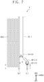
- FIGS. 7 to 9 For convenience in illustration, some regions of the detection line CDL, which are respectively indicated by the reference numbers 'A', 'B', and 'C' of FIG. 4 , are enlargedly illustrated in FIGS. 7 to 9 .
- the detection circuit CDC may be connected to at least one of the display signal pads DPD.
- the detection circuit CDC may be configured to compare data, which are obtained by measuring electrical resistance of the detection line CDL, and to provide a signal to one of the display signal pads DPD when a crack occurs.
- the signal may be used to drive the pixels PX connected to the display signal pad DPD. In other words, a signal alerting occurrence of a crack may be displayed on the display region DP-DA.
- the first line portion CDL1 and the input line SL1 may be provided at different levels.
- the first line portion CDL1 may be connected to the input line SL1 through a first interconnection contact hole CD-CHI.
- the first interconnection contact hole CD-CHI when viewed in a plan view, a region, in which the first interconnection contact hole CD-CHI is formed, will be referred to as a first contact region AR-CH1.
- the first interconnection contact hole CD-CHI may be formed by an etching process using plasma.
- a previously described element may be identified by a similar or identical reference number without repeating an overlapping description thereof.
- Other elements that are not separately described may be configured to have substantially the same technical features as those in the previously described embodiments.
Landscapes
- Engineering & Computer Science (AREA)
- Microelectronics & Electronic Packaging (AREA)
- Physics & Mathematics (AREA)
- Geometry (AREA)
- Manufacturing & Machinery (AREA)
- Computer Hardware Design (AREA)
- General Physics & Mathematics (AREA)
- Theoretical Computer Science (AREA)
- Electroluminescent Light Sources (AREA)
- Devices For Indicating Variable Information By Combining Individual Elements (AREA)
Abstract
Description
- The present disclosure relates to a display device, and in particular, to a display device with improved durability.
- Recently, various display devices, such as a liquid crystal display device, an organic electric field light-emitting display device, an electrowetting display device, a plasma display device, and an electrophoresis display device are being developed.
- During a process of fabricating a display device, various problems, such as disconnection or short circuit of a display signal line or pixel defect, may occur in the display device. An inspection or test process is performed to filter such problems in advance.
- By measuring properties of test interconnection lines that are formed on a specific region or an additional blank region of the display device, it is possible to examine electric characteristics of the display device and thereby to prevent or filter damage of an interconnection structure or electronic devices of the display device.
- Some embodiments of the inventive concept provide a display device with improved durability.
- According to some embodiments of the inventive concept, a display device may include a display panel including a display region and a non-display region enclosing the display region, when viewed in a plan view. The display panel may include an organic light emitting device or another light emitting device provided in the display region, circuit devices configured to drive the organic or other light emitting device, a detection line overlapped with the non-display region, detection pads connected to the detection line, and an input line connecting an input pad of the detection pads to the detection line. The detection line may include a first line portion provided at a level different from a level of the input line, the first line portion including an end portion, which is connected to the input line through a first interconnection contact hole in a first contact region, and a second line portion provided at a level different from the level of the first line portion and connected to the first line portion through a second interconnection contact hole in a second contact region. When viewed in the plan view, the first line portion may be provided closer to the display region than the second line portion, and a distance between the first line portion and the second line portion in a non-contact region may be less than a distance between the first interconnection contact hole and the second line portion. When used herein, the term different level especially refers to different layers of the display panel, especially different layers of a plurality of layers disposed on a substrate or a base layer.
- The detection line may be configured to indicate whether or not there is a damage, especially a crack in the interconnection structure and/or in an electronic device of the display device. Especially, the detection line may be connected or connectable to a detection circuit which may be configured to measure electrical resistance of the detection line and then to examine or determine based on the measurement result whether or not there is a damage, especially a crack.
- In some embodiments, the distance between the first line portion and the second line portion in the non-contact region may be less than a distance between the second interconnection contact hole and the second line portion.
- In some embodiments, the display panel may further include an output line connecting an output pad of the detection pads to the detection line, and the second line portion may include an end portion, which is connected to the first line portion, and an opposite end portion, which is connected to the output line.
- In some embodiments, the second line portion and the output line may be provided in the form of a single body.
- In some embodiments, when viewed in a plan view, that is in a view from the above onto the display region and the non-display region, at least a portion of the detection line may have a shape bent several times to form a branch. That is, the detection line may have for example the form of a meander, respectively of a plurality of meanders connected to each other.
- In some embodiments, the input line and the output line may be provided at a same level as the level of the second line portion.
- In some embodiments, the display device may further include a third line portion connecting the output line and the second line portion to each other. An end of the third line portion may be connected to an opposite end of the second line portion through a third interconnection contact hole, and an opposite end of the third line portion may be connected to the output line through a fourth interconnection contact hole.
- In some embodiments, the first line portion may be provided at a same level as a level of the third line portion.
- In some embodiments, when viewed in a plan view, the third line portion may be provided closer to the display region than the second line portion.
- In some embodiments, at least one of the first and second interconnection contact holes may be provided in plural respectively in a plurality.
- In some embodiments, the first interconnection contact hole may include a plurality of first interconnection contact holes, some of which have different sizes from each other. In other words, there may be provided a plurality of first interconnection contact holes, with the same size or with different sizes.
- In some embodiments, the second interconnection contact hole may include a plurality of second interconnection contact holes, some of which have different sizes from each other. In other words, there may be provided a plurality of second interconnection contact holes, which may have the same size or which may have different sizes.
- In some embodiments, the non-display region may include a first non-display region enclosing the display region, the detection line being provided in the first non-display region, and a second non-display region connected to the first non-display region, the second non-display region including a pad region, on which the detection pads may be provided, and a signal line region, on which the input line and output line may be provided.
- In some embodiments, the detection line may be provided in the first non-display region and the signal line region of the second non-display region, and the input line and the output line may be connected to the detection line, in the signal line region.
- In some embodiments, the non-display region may include a bending region, and the display panel may be bent about a bending axis in the bending region.
- In some embodiments, each of the detection line, the input line, and the output line may be provided in plural respectively in a plurality. Each of the detection lines may include a first detection line provided adjacent to a side region of the display region, and a second detection line provided adjacent to an opposite side region of the display region. The first and second detection lines may be connected to corresponding ones of the input and output lines.
- In some embodiments, the circuit devices may include a first transistor including a first input electrode, a first output electrode, a first control electrode, and a first semiconductor pattern, and a second transistor including a second input electrode, a second output electrode, a second control electrode, and a second semiconductor pattern. The first and second control electrodes may be electrically disconnected from the first and second semiconductor patterns by at least one insulating layer. The first control electrode may overlap with the first semiconductor pattern, when viewed in a plan view, and the second control electrode may overlap with the second semiconductor pattern, when viewed in a plan view.
- In some embodiments, the first line portion may be provided at a same level as a level of the first input electrode and the first output electrode.
- In some embodiments, the second line portion, the first control electrode, and the second control electrode may be provided at a same level.
- In some embodiments, the second control electrode may be provided on the second semiconductor pattern.
- In some embodiments, the first control electrode may be provided below the first semiconductor pattern.
- In some embodiments, the circuit devices may further include an upper electrode, which is provided on, and electrically disconnected from, the second control electrode, when viewed in a plan view. The upper electrode may be provided to overlap with the second control electrode to define a capacitor.
- In some embodiments, the second line portion may be provided at a same level as a level of the second control electrode, and the input line and the output line may be provided at a same level as a level of the first control electrode and the upper electrode.
- In some embodiments, the distance between the first interconnection contact hole and the second line portion and a distance between the second interconnection contact hole and the second line portion may be larger than or equal to 50 µm.
- According to some embodiments of the inventive concept, a display device may include a display panel including a display region and a non-display region enclosing the display region, when viewed in a plan view. The display panel may include a detection line, which is provided on the non-display region to enclose the display region, and in which a plurality of contact regions and a non-contact region adjacent to the contact regions are defined, detection pads connected to the detection line, and an input line and an output line connected to the detection pads. The detection line may include a first line portion provided at a level different from a level of the input line, the first line portion including an end portion, which is connected to the input line through an interconnection contact hole formed in a first contact region of the contact regions, and a second line portion provided at a level different from the level of the first line portion, the second line portion including an end portion, which is connected to the first line portion through an interconnection contact hole formed in a second contact region of the contact regions, and an opposite end portion, which is connected to the output line. A distance between the first line portion at the contact regions and the second line portion may be larger than a distance between the first line portion at the non-contact region and the second line portion.
- In some embodiments, a plurality of interconnection contact holes may be provided in each of the contact regions.
- In some embodiments, some of the plurality of interconnection contact holes may have different sizes from each other.
- According to some embodiments of the inventive concept, a display device may include a display panel including a display region and a non-display region enclosing the display region, when viewed in a plan view. The display panel may include an organic light emitting device or another light emitting device provided in the display region, circuit devices configured to drive the organic or other light emitting device, a detection line provided in the non-display region, an input pad and an output pad connected to the detection line, and an input line connecting the input pad to the detection line. The detection line may include a first line portion provided at a level different from a level of the input line, the first line portion including an end portion connected to the input line through a first interconnection contact hole in a first contact region, and a second line portion provided at a level different from the level of the first line portion, the second line portion including an end portion, which is connected to the first line portion through a second interconnection contact hole in a second contact region, and an opposite end portion, which is connected to the output pad. When viewed in the plan view, the first line portion may be provided closer to the display region than the second line portion, and a distance between the first line portion and the second line portion in a non-contact region may be less than a distance between the first interconnection contact hole and the second line portion.
- In some embodiments, the distance between the first line portion and the second line portion may be less than that between the second interconnection contact hole and the second line portion.
- According to some embodiments of the inventive concept, a display device may include a display panel including a display region and a non-display region enclosing the display region, when viewed in a plan view. The display panel may include an organic light emitting device or another light emitting device provided in the display region, circuit devices configured to drive the organic or other light emitting device, a detection line provided in the non-display region, detection pads connected to the detection line, and an input line and an output line connecting the detection pads to the detection line. The detection line may include a first line portion provided at a level different from a level of the input line, the first line portion including an end portion connected to the input line through a first interconnection contact hole in a first contact region, a second line portion provided at a level different from the level of the first line portion, the second line portion including an end portion connected to an opposite end portion of the first line portion through a second interconnection contact hole in a second contact region, and a third line portion provided at a level different from the level of the first line portion, the third line portion including an end portion, which is connected to an opposite end portion of the second line portion through a third interconnection contact hole, and an opposite end portion, which is connected to the output line through a fourth interconnection contact hole. A distance between the first line portion and the second line portion in a non-contact region may be less than a distance between one of the first to fourth interconnection contact holes and the second line portion.
- Example embodiments will be more clearly understood from the following brief description taken in conjunction with the accompanying drawings. The accompanying drawings represent non-limiting, example embodiments as described herein.
-
FIG. 1 is a perspective view of a display device according to some embodiments of the inventive concept. -
FIG. 2 is a sectional view of the display device shown inFIG. 1 . -
FIG. 3 is a sectional view of the display panel shown inFIG. 2 . -
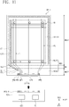
FIG. 4 is a plan view of the display panel shown inFIG. 3 . -
FIG. 5 is an equivalent circuit diagram of a pixel according to some embodiments of the inventive concept. -
FIG. 6 is an enlarged sectional view of a display panel according to some embodiments of the inventive concept. -
FIG. 7 is an enlarged view of a region 'A' ofFIG. 4 . -
FIG. 8 is an enlarged view of a region 'B' ofFIG. 4 . -
FIG. 9 is an enlarged view of a region 'C' ofFIG. 4 . -
FIG. 10 is a perspective view of a display device according to other embodiments of the inventive concept. -
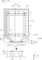
FIG. 11 is a plan view of a display panel according to other embodiments of the inventive concept. -
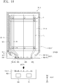
FIG. 12 is a plan view of a display panel according to other embodiments of the inventive concept. -
FIG. 13 is an enlarged view of a region 'B' ofFIG. 12 . -
FIG. 14 is a plan view of a display panel according to other embodiments of the inventive concept. -
FIG. 15 is an enlarged view of a region 'A' ofFIG. 14 . -
FIG. 16 is an enlarged view of a region 'A' according to other embodiments of the inventive concept. -
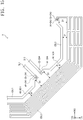
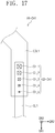
FIG. 17 is an enlarged view of a first contact region according to other embodiments of the inventive concept. -
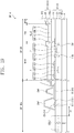
FIG. 18 is an enlarged sectional view of a display panel according to other embodiments of the inventive concept. -
FIG. 19 is an enlarged sectional view of a display panel according to other embodiments of the inventive concept. - It should be noted that these figures are intended to illustrate the general characteristics of methods, structure and/or materials utilized in certain example embodiments and to supplement the written description provided below. These drawings are not, however, to scale and may not precisely reflect the precise structural or performance characteristics of any given embodiment, and should not be interpreted as defining or limiting the range of values or properties encompassed by example embodiments. For example, the relative thicknesses and positioning of molecules, layers, regions and/or structural elements may be reduced or exaggerated for clarity. The use of similar or identical reference numbers in the various drawings is intended to indicate the presence of a similar or identical element or feature.
- Example embodiments of the inventive concepts will now be described more fully with reference to the accompanying drawings, in which example embodiments are shown. Example embodiments of the inventive concepts may, however, be embodied in many different forms and should not be construed as being limited to the embodiments set forth herein; rather, these embodiments are provided so that this disclosure will be thorough and complete, and will fully convey the concept of example embodiments to those of ordinary skill in the art. In the drawings, the thicknesses of layers and regions are exaggerated for clarity. Like reference numerals in the drawings denote like elements, and thus their description will be omitted.
- It will be understood that when an element is referred to as being "connected" or "coupled" to another element, it can be directly connected or coupled to the other element or intervening elements may be present. In contrast, when an element is referred to as being "directly connected" or "directly coupled" to another element, there are no intervening elements present. Like numbers indicate like elements throughout. As used herein the term "and/or" includes any and all combinations of one or more of the associated listed items. Other words used to describe the relationship between elements or layers should be interpreted in a like fashion (e.g., "between" versus "directly between," "adjacent" versus "directly adjacent," "on" versus "directly on").
- It will be understood that, although the terms "first", "second", etc. may be used herein to describe various elements, components, regions, layers and/or sections, these elements, components, regions, layers and/or sections should not be limited by these terms. These terms are only used to distinguish one element, component, region, layer or section from another element, component, region, layer or section. Thus, a first element, component, region, layer or section discussed below could be termed a second element, component, region, layer or section without departing from the teachings of example embodiments.
- Spatially relative terms, such as "beneath," "below," "lower," "above," "upper" and the like, may be used herein for ease of description to describe one element or feature's relationship to another element(s) or feature(s) as illustrated in the figures. It will be understood that the spatially relative terms are intended to encompass different orientations of the device in use or operation in addition to the orientation depicted in the figures. For example, if the device in the figures is turned over, elements described as "below" or "beneath" other elements or features would then be oriented "above" the other elements or features. Thus, the exemplary term "below" can encompass both an orientation of above and below. The device may be otherwise oriented (rotated 90 degrees or at other orientations) and the spatially relative descriptors used herein interpreted accordingly.
- The terminology used herein is for the purpose of describing particular embodiments only and is not intended to be limiting of example embodiments. As used herein, the singular forms "a," "an" and "the" are intended to include the plural forms as well, unless the context clearly indicates otherwise. It will be further understood that the terms "comprises", "comprising", "includes" and/or "including," if used herein, specify the presence of stated features, integers, steps, operations, elements and/or components, but do not preclude the presence or addition of one or more other features, integers, steps, operations, elements, components and/or groups thereof.
- Unless otherwise defined, all terms (including technical and scientific terms) used herein have the same meaning as commonly understood by one of ordinary skill in the art to which example embodiments of the inventive concepts belong. It will be further understood that terms, such as those defined in commonly-used dictionaries, should be interpreted as having a meaning that is consistent with their meaning in the context of the relevant art and will not be interpreted in an idealized or overly formal sense unless expressly so defined herein.
-
FIG. 1 is a perspective view of a display device DD according to some embodiments of the inventive concept. - Referring to
FIG. 1 , the display device DD may include a display surface DD-IS, which is used to display an image IM. The display surface DD-IS may be parallel to both of two different directions (e.g., a first direction DR1 and a second direction DR2). A normal direction of the display surface DD-IS (i.e., a thickness direction of the display device DD) will be referred to as a third direction DR3. - Hereinafter, the third direction DR3 may be used to differentiate a front or top surface of each element from a back or bottom surface. However, directions indicated by the first to third directions DR1, DR2, and DR3 may be relative concepts and may not be limited to the above example, and, for example, in certain embodiments, they may be changed to indicate other directions.
- As shown in
FIG. 1 , the display surface DD-IS may include a display region DD-DA, which is used to display the image IM, and a non-display region DD-NDA, which is placed adjacent to the display region DD-DA. The non-display region DDA-NDA may be configured not to display the image IM. In the display surface DD-IS, the non-display region DD-NDA may be defined to surround the display region DD-DA. As an example of the image IM, icon images are shown inFIG. 1 . -
FIG. 2 is a sectional view of the display device shown inFIG. 1 . -
FIG. 2 illustrates a vertical section defined by the second and third directions DR2 and DR3. In order to describe a stacking structure of a functional panel and/or functional units constituting the display device DD,FIG. 2 is illustrated in a simplified manner. - Referring to
FIG. 2 , the display device DD may include a display panel DP, an input sensing layer ISL, an anti-reflection panel RPP, and a window panel WP. The input sensing layer ISL may be provided on the display panel DP. The input sensing layer ISL and the display panel DP may be provided in an integrated or single-body structure, thereby constituting a display module DM. The display module DM, the anti-reflection panel RPP, and the window panel WP may be coupled to each other by an optically-transparent adhesive layer OCA. - The display panel DP may be configured to generate an image to be displayed to the outside, and the input sensing layer ISL may be configured to obtain coordinate information regarding an external input (e.g., touch event). Although not shown in the drawings, in certain embodiments, the display device DD may further include a protection structure placed on a bottom surface of the display panel DP. The protection structure and the display panel DP may be coupled to each other by an adhesive layer.
- According to some embodiments of the inventive concept, the display panel DP may be a light-emitting type display panel, but the inventive concept is not limited to a specific type of the display panel DP. For example, the display panel DP may be an organic light emitting display panel or a quantum dot light-emitting display panel. A light emitting layer of the organic light emitting display panel may include an organic light emitting material. A light emitting layer of the quantum dot light-emitting display panel may include quantum dots and/or quantum rods. For the sake of simplicity, the description that follows will refer to an example in which the display panel DP is the organic light emitting display panel.
- The anti-reflection panel RPP may be configured to reduce reflectance of an external light that is incident from an outer space to the window panel WP. Although not shown, in certain embodiments, the anti-reflection panel RPP may include a phase retarder and a polarizer. The phase retarder may be of a film type or a liquid crystal coating type and may include a λ/2 and/or λ/4 phase retarder. The polarizer may also be of a film type or a liquid crystal coating type. The polarizer of the film type may include an elongated synthetic resin film, whereas the polarizer of the liquid crystal coating type may include liquid crystals arranged with a specific orientation. The anti-reflection panel RPP may further include a protection film, in addition to the phase retarder and the polarizer.
- Although not shown, in certain embodiments, the anti-reflection panel RPP may further include color filters and a black matrix, which is provided adjacent to the color filters.
- The window panel WP may include a base film WP-BS and a light-blocking pattern WP-BZ. The base film WP-BS may include a glass substrate and/or a synthetic resin film. The base film WP-BS may not be limited to a single-layered structure. For example, in certain embodiments, the base film WP-BS may include two or more films that are bonded to each other by an adhesive film.
- The light-blocking pattern WP-BZ may be a colored organic layer. The light-blocking pattern WP-BZ may be formed by, for example, a coating method. Although not shown in the drawings, the window panel WP may further include a functional coating layer provided on the base film WP-BS. The functional coating layer may include an anti-fingerprint layer, an anti-reflection layer, a hard coating layer, and so forth.
-
FIG. 3 is a sectional view of the display panel DP shown inFIG. 2 . - Referring to
FIG. 3 , the display panel DP may include a base layer BL, a circuit device layer DP-CL provided on the base layer BL, a display device layer DP-OLED, and a thin-film encapsulation layer TFE. Although not shown in the drawings, the display panel DP may further include functional layers, such as an anti-reflection layer and a refractive index controlling layer. - The base layer BL may be formed of or include a synthetic resin film. For example, the base layer BL may include at least one of polyimide resins. However, the inventive concept is not limited to a specific material for the base layer BL. For example, the base layer BL may be formed of or include a glass substrate, a metal substrate, or an organic/inorganic composite substrate.
- The circuit device layer DP-CL may include at least one insulating layer and at least one circuit device. Hereinafter, an insulating layer in the circuit device layer DP-CL will be referred to as an intermediate insulating layer. The intermediate insulating layer may include at least one intermediate inorganic layer and/or at least one intermediate organic layer. The circuit device may include signal lines, pixel driving circuits, and so forth. The formation of the circuit device layer DP-CL may include forming an insulating layer, a semiconductor layer, and a conductive layer using a coating or deposition process and patterning the insulating layer, the semiconductor layer, and the conductive layer using a photolithography and etching process.
- The display device layer DP-OLED may be provided in a display region DP-DA. The display region DP-DA of the display panel DP may correspond to the display region DD-DA of the display device DD. The display device layer DP-OLED may include a plurality of light-emitting devices. The display device layer DP-OLED may include a plurality of organic light emitting diodes. The display device layer DP-OLED may further include an organic layer, such as a pixel definition layer.
- A thin-film encapsulation layer TFE may be provided to hermetically seal the display device layer DP-OLED. The thin-film encapsulation layer TFE may include at least one insulating layer. In some embodiments, the thin-film encapsulation layer TFE may include at least one inorganic layer (hereinafter, an inorganic encapsulation layer). The inorganic encapsulation layer may be used to protect the display device layer DP-OLED from moisture or oxygen. The inorganic encapsulation layer may include at least one of a silicon nitride layer, a silicon oxynitride layer, a silicon oxide layer, a titanium oxide layer, or an aluminum oxide layer, but the inventive concept is not limited thereto.
- However, the inventive concept is not limited to the example. For example, in certain embodiments, the thin-film encapsulation layer TFE may include at least one organic layer (hereinafter, an organic encapsulation layer). The organic encapsulation layer may be used to protect the display device layer DP-OLED from a contamination material such as dust particles. The organic encapsulation layer may include an acrylic organic layer, but the inventive concept is not limited thereto.
-
FIG. 4 is a plan view of the display panel shown inFIG. 3 . - Referring to
FIG. 4 , the display panel DP may include the display region DP-DA and a non-display region DP-NDA, when viewed in a plan view. As described above, the display region DP-DA of the display panel DP may correspond to the display region DD-DA of the display device DD. The non-display region DP-NDA of the display panel DP may correspond to the non-display region DD-NDA of the display device DD. - In the present embodiments, the non-display region DP-NDA may be defined along an edge of the display region DP-DA to surround the display region DP-DA.
- For example, the non-display region DP-NDA may include a first non-display region NDA1 and a second non-display region NDA2. The first non-display region NDA1 may be provided to surround the display region DP-DA. A detection line CDL to be described below may be provided in the first non-display region NDA1.
- The second non-display region NDA2 may be located at a side of the first non-display region NDA1 in the first direction DR1 and may be connected to the first non-display region NDA1. The second non-display region NDA2 may include a signal line region NDA-CL and a pad region NDA-PD. The pad region NDA-PD may be placed at an end region of the second non-display region NDA2 in the first direction DR1. However, the inventive concept is not limited to a specific position of the pad region NDA-PD.
- The display panel DP may include a driving circuit GDC, a plurality of signal lines DL, GL, PL, CSL, SL1, and SL2, a detection line CDL, a plurality of signal pads DP-PD, and a plurality of pixels PX.
- The pixels PX may be placed in the display region DP-DA. Each of the pixels PX may include an organic light emitting diode and a pixel driving circuit connected thereto. The driving circuit GDC, the signal lines DL, GL, PL, CSL, SL1, and SL2, the signal pads DP-PD, and the pixel driving circuit may be included in the circuit device layer DP-CL shown in
FIG. 3 . - The driving circuit GDC may be placed in the first non-display region NDA1. The driving circuit GDC may include a scan driving circuit. The scan driving circuit may be configured to generate a plurality of scan signals and sequentially output the scan signals to a plurality of scan lines GL to be described below. In addition, the scan driving circuit may be configured to output other control signals to a driving circuit of the pixel PX.
- The scan driving circuit may include a plurality of thin-film transistors that are formed by the same process as that for the driving circuit of the pixel PX (e.g., by a low temperature polycrystalline silicon (LTPS) process or a low temperature polycrystalline oxide (LTPO) process).
- The detection line CDL may be placed outside the driving circuit GDC. For example, the detection line CDL may be placed at an outermost region of the first non-display region NDA1. The detection line CDL will be described in more detail with reference to
FIGS. 6 to 9 . - The signal lines DL, GL, PL, CSL, SL1, and SL2 may include scan lines GL, data lines DL, a power line PL, a control signal line CSL, an input line SL1, and an output line SL2.
- Each of the scan lines GL may be connected to corresponding ones of the pixels PX, and each of the data lines DL may be connected to corresponding ones of the pixels PX. The power line PL may be connected to the pixels PX. The control signal line CSL may be used to provide control signals to the scan driving circuit. The signal pads DP-PD may be connected to end portions of the signal lines DL, GL, PL, CSL, SL1, and SL2. The signal pads DP-PD may include a scan signal pad GPD, a power pad PPD, display signal pads DPD, and detection pads PD1 and PD2.
- The scan signal pad GPD may be connected to the control signal line CSL. The power pad PPD may be connected to the power line PL. The display signal pads DPD may be connected to corresponding ones of the data lines DL. The detection pads PD1 and PD2 may be connected to the detection line CDL.
- Substantially, most of the signal lines DL, GL, PL, CSL, SL1, and SL2 may be the signal lines DL, GL, and PL connected to the pixels PX. The signal lines DL, GL, and PL connected to each pixel PX may be connected to transistors T1 and T2 (e.g., see
FIGS. 5 and6 ) of the pixel PX. Each of the signal lines DL, GL, and PL connected to the pixel PX may be provided to have a single- or multi-layered structure, may be provided in the form of a single body, or may include two or more portions. In the case of the two or more portions, they may be provided to form two or more different layers and may be connected to each other through a contact hole, which is formed to penetrate an insulating layer therebetween. - As shown in
FIG. 4 , a circuit board PCB electrically connected to the display panel DP may be provided. The circuit board PCB may be a rigid or flexible circuit board. The circuit board PCB may be directly coupled to the display panel DP or may be connected to the display panel DP through an additional circuit board. - A timing control circuit TC and a detection circuit CDC may be provided on the circuit board PCB. The timing control circuit TC may be configured to control an operation of the display panel DP, and the detection circuit CDC may be configured to measure electrical resistance of the detection line CDL and then to examine whether there is a crack, based on the measurement result. Each of the timing control circuit TC and the detection circuit CDC may be provided in the form of an integrated circuit chip and may be mounted on the circuit board PCB. Although not shown, an input sensing circuit (not shown) for controlling the input sensing layer ISL may be further provided in the circuit board PCB.
- The circuit board PCB may include circuit board pads PCB-P electrically connected to the display panel DP. Although not shown, the circuit board PCB may further include signal lines, which are provided to connect the circuit board pads PCB-P to the timing control circuit TC and/or the detection circuit CDC.
- However, the inventive concept is not limited to specific positions of the timing control circuit TC and the detection circuit CDC. For example, although not shown in the drawings, in certain embodiments, the timing control circuit TC and the detection circuit CDC may be mounted on the non-display region DP-NDA of the display panel DP.
-
FIG. 5 is an equivalent circuit diagram of a pixel according to some embodiments of the inventive concept. -
FIG. 5 illustrates an example, in which one scan line GL, one data line DL, one power line PL, and one pixel PX connected thereto are provided. However, the structure of the pixel PX is not limited to that shown inFIG. 5 , and in certain embodiments, it may be variously changed. - An organic light emitting diode OLED may be a top-emission type diode or a bottom-emission type diode. The pixel PX may include a first or switching transistor T1, a second or driving transistor T2, and a capacitor Cst, which are used as a pixel driving circuit for driving the organic light emitting diode OLED. A first power voltage ELVDD may be provided to the second transistor T2, and a second power voltage ELVSS may be provided to the organic light emitting diode OLED. The second power voltage ELVSS may be lower than the first power voltage ELVDD.
- If a scan signal is applied to the scan line GL, the first transistor T1 may output a data signal applied to the data line DL in response to the scan signal. The capacitor Cst may be charged to have a voltage corresponding to the data signal, which is transmitted from the first transistor T1. The second transistor T2 may be connected to the organic light emitting diode OLED. The second transistor T2 may control a driving current flowing through the organic light emitting diode OLED, based on an amount of charge stored in the capacitor Cst.
- The equivalent circuit of
FIG. 5 is just one of possible equivalent circuits of the pixel, but the inventive concept is not limited thereto. The pixel PX may be configured to further include at least one transistor or at least one capacitor. In certain embodiments, the organic light emitting diode OLED may be coupled to the power line PL and the second transistor T2. -
FIG. 6 is an enlarged sectional view of a display panel according to some embodiments of the inventive concept. - Referring to
FIG. 6 , the circuit device layer DP-CL, the display device layer DP-OLED, and the thin-film encapsulation layer TFE may be sequentially placed on the base layer BL. In the present embodiments, the circuit device layer DP-CL may include a buffer layer BFL made of an inorganic layer, a first intermediateinorganic layer 10, a second intermediateinorganic layer 20, and an intermediateorganic layer 30 made of an organic layer. The inorganic and organic layers may not be limited to specific materials, and in certain embodiments, the buffer layer BFL may be optionally provided or omitted. - The first transistor T1 and the second transistor T2 may include a semiconductor pattern OSP1 (hereinafter, a first semiconductor pattern) and a semiconductor pattern OSP2 (hereinafter, a second semiconductor pattern), respectively, which are provided on the buffer layer BFL. The first semiconductor pattern OSP1 and the second semiconductor pattern OSP2 may be formed of or include at least one of amorphous silicon, poly silicon, or metal oxide semiconductor materials.
- The first intermediate
inorganic layer 10 may be provided on the first semiconductor pattern OSP1 and the second semiconductor pattern OSP2. The first transistor T1 and the second transistor T2 may include a control electrode GE1 (hereinafter, a first control electrode) and a control electrode GE2 (hereinafter, a second control electrode), respectively, which are provided on the first intermediateinorganic layer 10. The first control electrode GE1 and the second control electrode GE2 may be formed using the photolithography process as that for forming the scan lines GL ofFIG. 5 . - The second intermediate
inorganic layer 20 may be provided on the first intermediateinorganic layer 10 to cover the first control electrode GE1 and the second control electrode GE2. The first transistor T1 may include an input electrode DEI (hereinafter, a first input electrode) and an output electrode SE1 (hereinafter, a first output electrode) provided on the second intermediateinorganic layer 20, and the second transistor T2 may include an input electrode DE2 (hereinafter, a second input electrode) and an output electrode SE2 (hereinafter, a second output electrode) provided on the second intermediateinorganic layer 20. - A first contact hole CH1 and a second contact hole CH2 may be formed to penetrate both of the first and second intermediate
inorganic layers inorganic layers - In
FIG. 6 , the first transistor T1 and the second transistor T2 are illustrated to have a top gate structure, in which the first and second control electrodes GE1 and GE2 are provided on the first and second semiconductor patterns OSP1 and OSP2, respectively, but the inventive concept is not limited thereto. For example, in certain embodiments, at least one of the first transistor T1 and the second transistor T2 may be modified to have a bottom gate structure. This will be described in more detail with reference toFIG. 19 . - The intermediate
organic layer 30 may be provided on the second intermediateinorganic layer 20 to cover the first input electrode DEI, the second input electrode DE2, the first output electrode SE1, and the second output electrode SE2. The intermediateorganic layer 30 may be provided to have a flat surface. - The display device layer DP-OLED may be provided on the intermediate
organic layer 30. The display device layer DP-OLED may include a pixel definition layer PDL and the organic light emitting diode OLED. The pixel definition layer PDL may be formed of or include an organic material. A first electrode AE may be provided on the intermediateorganic layer 30. The first electrode AE may be connected to the second output electrode SE2 through a fifth contact hole CH5 penetrating the intermediateorganic layer 30. An opening OP may be defined in the pixel definition layer PDL. The opening OP of the pixel definition layer PDL may be provided to expose at least a portion of the first electrode AE. In certain embodiments, the pixel definition layer PDL may be omitted. - The pixel PX may be placed in the display region DP-DA. The display region DP-DA may include a light-emitting region PXA and a non-light-emitting region NPXA adjacent to the light-emitting region PXA. The non-light-emitting region NPXA may be provided to surround the light-emitting region PXA. In the present embodiments, the light-emitting region PXA may be defined to correspond to a region of the first electrode AE exposed by the opening OP.
- In certain embodiments, the light-emitting region PXA may be overlapped with at least one of the first and second transistors T1 and T2. For example, the opening OP may be enlarged, and not only the first electrode AE but also a light emitting layer EML to be described below may also be enlarged.
- The light emitting layer EML may be provided on a region corresponding to the opening OP. In other words, the light emitting layer EML may have an isolated structure that is provided for each of the pixels PX. The light emitting layer EML may include an organic material and/or an inorganic material. The light emitting layer EML may be configured to generate a specific color light.
- In the present embodiments, the light emitting layer EML is illustrated to have a patterned structure, but the light emitting layer EML may be provided in common on a plurality of the pixels PX. Here, the light emitting layer EML may be configured to generate a white-color light. Also, the light emitting layer EML may have a multi-layered structure called 'tandem'.
- A second electrode CE may be provided on the light emitting layer EML. The second electrode CE may be provided in common on a plurality of the pixels PX.
- The thin-film encapsulation layer TFE may be provided on the second electrode CE. The thin-film encapsulation layer TFE may be provided in common on a plurality of the pixels PX. In the present embodiments, the thin-film encapsulation layer TFE may be provided to directly cover the second electrode CE. In some embodiments, a capping layer may be provided between the thin-film encapsulation layer TFE and the second electrode CE, thereby covering the second electrode CE. Here, the thin-film encapsulation layer TFE may be provided to directly cover the capping layer.
- According to some embodiments of the inventive concept, although not shown in the drawings, the display device layer DP-OLED may further include a hole control layer (not shown) and an electron control layer (not shown), which are provided on and below the light emitting layer EML.
-
FIG. 7 is an enlarged view of a region 'A' ofFIG. 4 , andFIG. 8 is an enlarged view of a region 'B' ofFIG. 4 .FIG. 9 is an enlarged view of a region 'C' ofFIG. 4 . - For convenience in illustration, some regions of the detection line CDL, which are respectively indicated by the reference numbers 'A', 'B', and 'C' of
FIG. 4 , are enlargedly illustrated inFIGS. 7 to 9 . - In
FIG. 6 , a sectional view taken along line I-I' ofFIG. 7 is illustrated. - Referring to
FIGS. 4 and6 to 9 , the detection line CDL may be provided on the first non-display region NDA1 to enclose the display region DP-DA. For example, in the present embodiments, the detection line CDL may be provided on regions of the first non-display region NDA1, except for a region adjacent to the second non-display region NDA2. - The detection line CDL may be connected to the input line SL1 and the output line SL2. The input line SL1 and the output line SL2 may be connected to the detection pads PD1 and PD2. In detail, the input line SL1 may be connected to an input pad PD1, and the output line SL2 may be connected to an output pad PD2. The input pad PD1 and the output pad PD2 may be connected to the detection circuit CDC.
- In some embodiments, the detection circuit CDC may be connected to at least one of the display signal pads DPD. The detection circuit CDC may be configured to compare data, which are obtained by measuring electrical resistance of the detection line CDL, and to provide a signal to one of the display signal pads DPD when a crack occurs. The signal may be used to drive the pixels PX connected to the display signal pad DPD. In other words, a signal alerting occurrence of a crack may be displayed on the display region DP-DA.
- In the present embodiments, the input pad PD1 and the output pad PD2 may be arranged in or along the second direction DR2, at a side region of the pad region NDA-PD. Furthermore, the input line SL1 and the output line SL2, which are connected to the input pad PD1 and the output pad PD2, respectively, may be extended to be inclined toward a side region of the display panel DP in the second direction DR2 and may be connected to the detection line CDL provided in the first non-display region NDA1. The inventive concept is not limited to the specific positions of the input pad PD1 and the output pad PD2.
- In the present embodiments, the detection line CDL may include a first line portion CDL1 and a second line portion CDL2. The first line portion CDL1 and the second line portion CDL2 may extend along the edge region of the display region DP-DA. The first line portion CDL1 may be positioned closer to the display region DP-DA than the second line portion CDL2.
- The first line portion CDL1 may be connected to the input line SL1. For example, an end of the first line portion CDL1 may be connected to the input line SL1, at a side region of the first non-display region NDA1 in the second direction DR2.
- The first line portion CDL1 and the input line SL1 may be provided at different levels. The first line portion CDL1 may be connected to the input line SL1 through a first interconnection contact hole CD-CHI.
- For example, the first line portion CDL1 may be provided at the same level as that of the input electrodes DEI and DE2 and the output electrodes SE1 and SE2 of the first and second transistors T1 and T2. The input line SL1 and the output line SL2 may be provided at the same level as that of the control electrodes GE1 and GE2 of the first and second transistors T1 and T2.
- In some embodiments, the display panel DP may further include at least one dam portion (e.g., see DM1 and DM2 of
FIG. 6 ) provided on the non-display region DP-NDA. The dam portions DM1 and DM2 may be provided closer to the display region DP-DA than the detection line CDL. Although not shown inFIG. 4 , the dam portions DM1 and DM2 may extend along the edge region of the display region DP-DA. The dam portions DM1 and DM2 may prevent the thin-film encapsulation layer TFE from overflowing to the out side of the dam portions DM1, DM2. - As shown in
FIG. 7 , when viewed in a plan view, a region, in which the first interconnection contact hole CD-CHI is formed, will be referred to as a first contact region AR-CH1. In the present embodiments, the first interconnection contact hole CD-CHI may be formed by an etching process using plasma. - As shown in
FIG. 9 , the first line portion CDL1 may be connected to the second line portion CDL2. For example, an opposite end of the first line portion CDL1 may be connected to an end of the second line portion CDL2, at an opposite side region of the first non-display region NDA1 in the second direction DR2. - The first line portion CDL1 and the second line portion CDL2 may be provided at different levels. The first line portion CDL1 may be connected to the second line portion CDL2 through a second interconnection contact hole CD-CH2. The second line portion CDL2 may be provided at the same level as that of the input line SL1 and the output line SL2.
- When viewed in a plan view, a region, in which the second interconnection contact hole CD-CH2 is formed, will be referred to as a second contact region AR-CH2. The remaining regions on the detection line CDL, except for the first and second contact regions AR-CH1 and AR-CH2, will be referred to as a non-contact region AR-NCH. In the present embodiments, the second interconnection contact hole CD-CH2 may be formed by an etching process using plasma.
- In the present embodiments, the first line portion CDL1 and the second line portion CDL2 may be provided at different levels. For example, the first line portion CDL1 and the second line portion CDL2 may be formed of or include different materials. Accordingly, it may be possible to suppress or prevent the first and second line portions CDL1 and CDL2 from being capacitively coupled to each other.
- The second line portion CDL2 may be provided in the form of a densely-packed infill pattern including a plurality of linear segments, each of which is extended from another (e.g., at right angle). In other words, the second line portion CDL2 has a bent shape a plurality of times in the form of a branch. Due to the bending structure formed by the linear segments of the second line portion CDL2, the second line portion CDL2 may have a large occupation area on the first non-display region NDA1, even when it does not have a large thickness. This make it possible to more precisely detect a crack over an outer region of the display panel DP.
- In the present embodiments, the bended portions of the second line portion CDL2 may be arranged in an extension direction of the first line portion CDL1 or along an outer edge of the display region DP-DA, but the inventive concept is not limited thereto. For example, shapes, extension and bending directions, and the bending number of the bended portions of the second line portion CDL2 may be variously changed.
- The second line portion CDL2 may be connected to the output line SL2. For example, an opposite end of the second line portion CDL2 may be connected to the output line SL2, at a side region of the first non-display region NDA1 in the second direction DR2.
- The second line portion CDL2 may be provided at the same level as that of the output line SL2. Furthermore, the second line portion CDL2 and the output line SL2 may be provided to form a single body at the same level.
- In the present embodiments, a distance between a first line portion CDL1 and a second line portion CDL2 may be changed depending on whether or not there are the contact regions AR-CH1 and AR-CH2.
- In detail, a distance between the first line portion CDL1 positioned in the first or second contact region AR-CH1 or AR-CH2 and the second line portion CDL2 positioned in the non-contact region AR-NCH will be referred to as a first distance D1. Also, a distance between the first and second line portions CDL1 and CDL2 positioned in the non-contact region AR-NCH will be referred to as a second distance D2. In the present embodiments, the first distance D1 may be larger than the second distance D2.
- In other words, a distance D1 between the first interconnection contact hole CD-CHI in the first contact region AR-CH1 and the second line portion CDL2 in the non-contact region (not shown) may be larger than a distance D2 between the first line portion CDL1 and the second line portion CDL2 in the non-contact region AR-NCH. A distance D1 between the second interconnection contact hole CD-CH2 in the second contact region AR-CH2 and the second line portion CDL2 in the non-contact region (not shown) may be larger than a distance D2 between the first and second line portions CDL1 and CDL2 in the non-contact region (not shown).
- In the present embodiments, the larger the first distance D1, the better. If the first distance D1 is increased, it may be possible to reduce a frequency of static electricity discharging (ESD) occurring in the detection line CDL. In some embodiments, the first distance D1 may be set to the largest distance by which the first line portion CDL1 and the second line portion CDL2 can be spaced apart from each other on the first non-display region NDA1.
- In some embodiments, the first distance D1 may be larger than or equal to about 50 µm, and the second distance D2 may be less than or equal to about 10 µm.
- Although not shown, in certain embodiments, additional lines may be further provided between the first line portion CDL1 and the display region DP-DA. In this case, a third distance, which is defined as a distance between the first line portion CDL1 in the contact regions AR-CH1 and AR-CH2 and the additional lines, may be larger than a fourth distance, which is defined as a distance between the first line portion CDL1 in the non-contact region AR-NCH and the additional lines. For example, the third distance may be larger than or equal to about 50 µm, and the fourth distance may be less than or equal to about 10 µm.
- In general, the static electricity discharging (ESD) may occur frequently in the contact regions AR-CH1 and AR-CH2. In detail, electric charges may be accumulated in an end of each of the first line portion CDL1, the second line portion CDL2 and the input lines SL1 provided in the contact regions AR-CH1 and AR-CH2. In such a case, if a plasma etching process is performed to form the first and second interconnection contact holes CD-CHI and CD-CH2, reactive materials in plasma may be charged by the electric charges accumulated in the end of each of the first line portion CDL1, the second line portion CDL2 and the input lines SL1.
- In the case where, unlike the previously described embodiments of the inventive concept, the distance between the first line portion CDL1 and the second line portion CDL2 is uniform, due to the static electricity discharging (ESD), which may occur in the contact regions AR-CH1 and AR-CH2, a crack may be formed in the second line portion CDL2 provided in the non-contact region AR-NCH. By contrast, according to some embodiments of the inventive concept, the distance D1 between the first interconnection contact hole CD-CHI in the first contact region AR-CH1 and the second line portion CDL2 in the non-contact region AR-NCH may be larger than the distance D2 between the first and second line portions CDL1 and CDL2 in the non-contact region AR-NCH. In this case, it may be possible to suppress or prevent a crack from occurring in the second line portion CDL2. In other words, it may be possible to improve durability or reliability of the display device.
-
FIG. 10 is a perspective view of a display module DM-1 according to other embodiments of the inventive concept, andFIG. 11 is a plan view of a display panel DP-1 according to other embodiments of the inventive concept. - For concise description, a previously described element may be identified by a similar or identical reference number without repeating an overlapping description thereof. Other elements that are not separately described may be configured to have substantially the same technical features as those in the previously described embodiments.
- Referring to
FIGS. 10 and11 , the display module DM-1 may include a plurality of regions which are defined depending on its operation mode. For example, the display module DM-1 may include a first region NBA1, a second region NBA2, and a third region BA between the first and second regions NBA1 and NBA2. The third region BA may be configured to be bent about a bending axis BX and may be a region that is configured to have a variable curvature. The first region NBA1, the second region NBA2, and the third region BA may be referred to as a first non-bending region NBA1, a second non-bending region NBA2, and a bending region BA, respectively. In the present embodiments, the first non-bending region NBA1 may be overlapped with the first non-display region NDA1 and the display region DP-DA, and the bending region BA and the second non-bending region NBA2 may be overlapped with the second non-display region NDA2. - The display module DM-1 may be configured to be bent in an outer-bending manner, allowing the display surface DD-IS to be exposed to the outside. In the present embodiments, it may be possible to reduce an area of a bezel of the display device.
-
FIG. 12 is a plan view of a display panel DP-2 according to other embodiments of the inventive concept, andFIG. 13 is an enlarged view of a region 'B' ofFIG. 12 . - For concise description, a previously described element may be identified by a similar or identical reference number without repeating an overlapping description thereof. Other elements that are not separately described may be configured to have substantially the same technical features as those in the previously described embodiments.
- Referring to
FIGS. 12 and13 , according to other embodiments of the inventive concept, a plurality of detection lines CDL-2 may be provided. - For example, the detection lines CDL-2 may include a first detection line CDLA and a second detection line CDLB. The first detection line CDLA may be provided at a side region of the first non-display region NDA1 in the second direction DR2 to enclose a side region of the display region DP-DA in the second direction DR2.
- The second detection line CDLB may be provided at an opposite side region of the first non-display region NDA1 in the second direction DR2 to enclose an opposite side region of the display region DP-DA in the second direction DR2.
- In the present embodiments, the input and output lines SL1 and SL2 of the first detection line CDLA may be provided at a side region of the signal line region NDA-CL in the second direction DR2, and the input and output lines SL1 and SL2 of the second detection line CDLB may be provided at an opposite side region of the signal line region NDA-CL in the second direction DR2.
- Also, in the present embodiments, the detection pads PD1 and PD2 connected to the first detection line CDLA may be provided at a side region of the pad region NDA-PD in the second direction DR2, and the detection pads PD1 and PD2 connected to the second detection line CDLB may be provided at an opposite side region of the pad region NDA-PD in the second direction DR2.
- The line portions CDL1 and CDL2 of the first detection line CDLA may have substantially the same structure as those of the second detection line CDLB. Thus, for concise description, only the region 'B' of the first detection line CDLA is illustrated in
FIG. 13 . - In the present embodiments, an example, in which a pair of the detection lines CDLA and CDLB are provided, have been described, but the inventive concept is not limited thereto. In certain embodiments, three or more detection lines may be provided in the non-display region DP-NDA.
-
FIG. 14 is a plan view of a display panel DP-3 according to other embodiments of the inventive concept, andFIG. 15 is an enlarged view of a region 'A' ofFIG. 14 . - Referring to
FIGS. 14 and15 , a display panel DP-3 according to other embodiments of the inventive concept may include a detection line CDL-3 that is provided in the signal line region NDA-CL of the second non-display region NDA2 and the first non-display region NDA1. In the signal line region NDA-CL, the detection line CDL-3 may be connected to the input line SL1 and the output line SL2. - In the present embodiments, an end of the first line portion CDL1 may be connected to the input line SL1, at a side region of the signal line region NDA-CL in the second direction DR2.
- An opposite end of the first line portion CDL1 may be connected to an end of the second line portion CDL2, at an opposite side region of the signal line region NDA-CL in the second direction DR2.
- In the present embodiments, the detection line CDL-3 may further include a third line portion CDL3. The third line portion CDL3 may be connected to the second line portion CDL2 and the output line SL2.
- In detail, an opposite end of the second line portion CDL2 may be connected to an end of the third line portion CDL3, at a side region of the signal line region NDA-CL in the second direction DR2.
- The third line portion CDL3 may be provided at a different level from that of the second line portion CDL2. The third line portion CDL3 may be connected to the second line portion CDL2 through a third interconnection contact hole CD-CH3. When viewed in a plan view, a region, in which the third interconnection contact hole CD-CH3 is formed, may be referred to as a third contact region AR-CH3.
- In the present embodiments, the third line portion CDL3 may be provided at the same level as that of the first line portion CDL1. For example, the third line portion CDL3 may be provided at the same level as that of the input electrodes DEI and DE2 and the output electrodes SE1 and SE2 of the first and second transistors T1 and T2.
- The third line portion CDL3 may be connected to the output line SL2. In detail, an end of the third line portion CDL3 may be connected to the output line SL2, at a side region of the signal line region NDA-CL in the second direction DR2.
- The third line portion CDL3 and the output line SL2 may be provided at different levels. The third line portion CDL3 may be connected to the output line SL2 through a fourth interconnection contact hole CD-CH4. When viewed in a plan view, a region, in which the fourth interconnection contact hole CD-CH4 is formed, will be referred to as a fourth contact region AR-CH4.
- In the present embodiments, a distance between the third line portion CDL3 positioned in the third or fourth contact region AR-CH3 or AR-CH4 and the second line portion CDL2 positioned in the non-contact region AR-NCH may be equal to the first distance D1. Also, a distance between the third and second line portions CDL3 and CDL2 positioned in the non-contact region AR-NCH may be equal to the second distance D2.
- In the present embodiments, the detection line CDL-3 extends to the signal line region NDA-CL of the second non-display region NDA2 beyond the first non-display region NDA1. That is, since the area where the detection line CDL-3 is disposed on the display panel DP is increased, it may be possible to more precisely determine whether a crack is formed in the display panel DP.
-
FIG. 16 is an enlarged view of a region 'A' according to other embodiments of the inventive concept. - For concise description, a previously described element may be identified by a similar or identical reference number without repeating an overlapping description thereof. Other elements that are not separately described may be configured to have substantially the same technical features as those in the previously described embodiments.
- For convenience in illustration, only one (e.g., the first contact region AR-CH1) of the plurality of contact regions is illustrated in
FIG. 16 . For the sake of simplicity, the description that follows will refer to only the first contact region AR-CH1, but other contact regions may be configured to have substantially the same features as those of the first contact region AR-CH1 to be described herein. - According to other embodiments of the inventive concept, as shown in
FIG. 16 , a plurality of first interconnection contact holes CD-CHI may be formed in the first contact region AR-CH1. The plurality of first interconnection contact holes CD-CHI may be used to connect the input line SL1 and the first line portion CDL1 to each other. - In this case, even when some of the plurality of contact holes CD-CHI are damaged, the input line SL1 and the first line portion CDL1 may be electrically connected to each other by the remaining undamaged ones of the contact holes CD-CHI. That is, as described above, the plurality of interconnection contact holes CD-CHI are used to connect the input line SL1 to the first line portion CDL1, it may be possible to improve durability or reliability of the detection line CDL.
-
FIG. 17 is an enlarged view of a first contact region AR-CH1 according to other embodiments of the inventive concept. - For concise description, a previously described element may be identified by a similar or identical reference number without repeating an overlapping description thereof. Other elements that are not separately described may be configured to have substantially the same technical features as those in the previously described embodiments.
- For convenience in illustration, only one (e.g., the first contact region AR-CH1) of the plurality of contact regions is illustrated in
FIG. 17 . For the sake of simplicity, the description that follows will refer to only the first contact region AR-CH1, but other contact regions may be configured to have substantially the same features as those of the first contact region AR-CH1 to be described herein. - According to other embodiments of the inventive concept, as shown in
FIG. 17 , a plurality of first interconnection contact holes CD-CHI may be formed in the first contact region AR-CH1. The first interconnection contact holes CD-CHI may be used to connect the input line SL1 and the first line portion CDL1 to each other. - In the present embodiments, the first interconnection contact holes CD-CHI may include interconnection contact holes CH_1, CH_2, CH_3, CH_4, and CH_5 having different sizes from each other. Although
FIG. 17 illustrates an example in which all of the first interconnection contact holes CH_1 - CH_5 are formed to have different sizes from each other, at least some of the first interconnection contact holes CH_1 - CH_5 may be provided to have different sizes from each other. -
FIG. 18 is an enlarged sectional view of a display panel DP-3 according to other embodiments of the inventive concept. - For concise description, a previously described element may be identified by a similar or identical reference number without repeating an overlapping description thereof. Other elements that are not separately described may be configured to have substantially the same technical features as those in the previously described embodiments.
- Referring to
FIG. 18 , the circuit device layer DP-CL may include the buffer layer BFL, the first intermediateinorganic layer 10, the intermediateorganic layer 30, and second intermediate inorganic layers 20-1, 20-2, and 20-3. The second intermediate inorganic layers 20-1, 20-2, and 20-3 may include a first intermediate layer 20-1, a second intermediate layer 20-2, and a third intermediate layer 20-3. - The second semiconductor pattern OSP2 of the second transistor T2 may be provided on the buffer layer BFL. The first intermediate
inorganic layer 10 may be provided on the second semiconductor pattern OSP2. The second control electrode GE2 and the second line portion CDL2 may be provided on the first intermediateinorganic layer 10. The second control electrode GE2 may be overlapped with the display region DP-DA, and the second line portion CDL2 may be overlapped with the non-display region DP-NDA. - The first intermediate layer 20-1 may be provided on the first intermediate
inorganic layer 10 to cover the second control electrode GE2 and the second line portion CDL2. The first semiconductor pattern OSP1 of the first transistor T1 may be provided on the first intermediate layer 20-1. The second intermediate layer 20-2 may be provided on the first intermediate layer 20-1 to cover the first semiconductor pattern OSP1. - In the present embodiments, the circuit device layer DP-CL may further include an upper electrode UE. The first control electrode GE1 and the upper electrode UE may be provided on the second intermediate layer 20-2. The first control electrode GE1 may be overlapped with the first semiconductor pattern OSP1. The upper electrode UE may be overlapped with the second control electrode GE2, when viewed in a plan view. Since the upper electrode UE is provided on the second control electrode GE2, the upper electrode UE and the second control electrode GE2 may constitute a capacitor. In other words, an electric field may be produced between overlapped portions of the upper electrode UE and the second control electrode GE2. The capacitor may correspond to the capacitor Cst of
FIG. 5 . - In the present embodiments, the second control electrode GE2 may be used not only as a part of the second transistor T2 but also as one electrode of the capacitor Cst.
- The third intermediate layer 20-3 may be provided on the second intermediate layer 20-2 to cover the first control electrode GE1 and the upper electrode UE. The first input and output electrodes DEI and SE1 of the first transistor T1, the second input and output electrodes DE2 and SE2 of the second transistor T2, and the first line portion CDL1 of the detection line CDL may be provided on the third intermediate layer 20-3. The input electrodes DEI and DE2 and the output electrodes SE1 and SE2 of the first and second transistors T1 and T2 may be overlapped with the display region DP-DA, and the first line portion CDL1 may be overlapped with the non-display region DP-NDA.
- The first input electrode DEI and the first output electrode SE1 may be connected to two different portions of the first semiconductor pattern OSP1 through the first contact hole CH1 and the second contact hole CH2, respectively, which are formed to penetrate both of the second and third intermediate layers 20-2 and 20-3. The second input electrode DE2 and the second output electrode SE2 may be connected to two different portions of the second semiconductor pattern OSP2 through the third contact hole CH3 and the fourth contact hole CH4, respectively, which are formed to penetrate the first intermediate
inorganic layer 10 and the first to third intermediate layers 20-1, 20-2, and 20-3. - The intermediate
organic layer 30 may be provided on the second intermediate inorganic layers 20-1, 20-2, and 20-3 to cover the first input electrode DEI, the second input electrode DE2, the first output electrode SE1, and the second output electrode SE2. The intermediateorganic layer 30 may be provided to have a flat surface. -
FIG. 19 is an enlarged sectional view of a display panel DP-4 according to other embodiments of the inventive concept. - For concise description, a previously described element may be identified by a similar or identical reference number without repeating an overlapping description thereof. Other elements that are not separately described may be configured to have substantially the same technical features as those in the previously described embodiments.
- Referring to
FIG. 19 , the first transistor T1 according to other embodiments of the inventive concept may have a bottom gate structure. In other words, the first semiconductor pattern OSP1 of the first transistor T1 may be provided on the first control electrode GE1. - In detail, the first transistor T1 may include the first control electrode GE1 provided on the first intermediate
inorganic layer 10, the first semiconductor pattern OSP1 provided on the second intermediateinorganic layer 20, and the first input electrode DEI and the first output electrode SE1 provided on the intermediateorganic layer 30. The first control electrode GE1 may be provided between the first intermediateinorganic layer 10 and the second intermediateinorganic layer 20. - The first semiconductor pattern OSP1 may be provided on the first control electrode GE1. The first semiconductor pattern OSP1 may be overlapped with the first control electrode GE1, when viewed in a plan view. The first input and output electrodes DEI and SE1 may be provided on the second intermediate
inorganic layer 20 to partially cover two portions of the first semiconductor pattern OSP1. Although not shown, the first transistor T1 may further include an ohmic contact layer which is formed between the first semiconductor pattern OSP1 and the first input and output electrodes DEI and SE1. - The second transistor T2 may correspond to the second transistor T2 shown in
FIG. 6 . For concise description, description of overlapping elements previously described may be omitted. - in the present embodiments, the first line portion CDL1 may be provided at the same level as that of the first semiconductor pattern OSP1, the first input electrode DE1 and the first output electrode SE1.
- According to some embodiments of the inventive concept, it may be possible to improve durability of a display device.
- While example embodiments of the inventive concepts have been particularly shown and described, it will be understood by one of ordinary skill in the art that variations in form and detail may be made therein without departing from the scope of the attached claims.
Claims (15)
- A display device (DD), comprising a display panel (DP) including a display region (DP-DA) and a non-display region (DP-NDA) enclosing the display region (DP-DA), when viewed in a plan view,
wherein the display panel (DP) comprises:an organic light emitting device or another light emitting device provided in the display region (DP-DA);circuit devices configured to drive the organic or other light emitting device;a detection line (CDL) overlapped with the non-display region (DP-NDA);detection pads (PD1, PD2) connected to the detection line (CDL); andan input line (SL1) connecting an input pad (PD1) of the detection pads (PD1, PD2) to the detection line (CDL),wherein the detection line (CDL) comprises:a first line portion (CDL1) provided at a level different from a level of the input line (SL1), the first line portion (CDL1) including an end portion, which is connected to the input line (SL1) through a first interconnection contact hole (CD-CH1) in a first contact region (AR-CH1); anda second line portion (CDL2) provided at a level different from the level of the first line portion (CDL1) and connected to the first line portion (CDL1) through a second interconnection contact hole (CD-CH2) in a second contact region (AR-CH2),wherein, when viewed in the plan view, the first line portion (CDL1) is provided closer to the display region (DP-DA) than the second line portion (CDL2), anda distance (D2) between the first line portion (CDL1) and the second line portion (CDL2) in a non-contact region (AR-NCH) is less than a distance (D1) between the first interconnection contact hole (CD-CH1) and the second line portion (CDL2). - The display device (DD) of claim 1, wherein the distance (D2) between the first line portion (CDL1) and the second line portion (CDL2) in the non-contact region (AR-NCH) is less than a distance (D1) between the second interconnection contact hole (CD-CH2) and the second line portion (CDL2).
- The display device (DD) of claim 1 or 2, wherein the display panel (DP) further comprises an output line (SL2) connecting an output pad (PD2) of the detection pads (PD1, PD2) to the detection line (CDL), and
the second line portion (CDL2) includes an end portion, which is connected to the first line portion (CDL1), and an opposite end portion, which is connected to the output line (SL2). - The display device (DD) of claim 3, wherein the second line portion (CDL2) and the output line (SL2) are provided in the form of a single body.
- The display device (DD) of at least one of claims 1 to 4, wherein, when viewed in a plan view, at least a portion of the detection line (CDL) has a shape bent several times to form of a branch.
- The display device (DD) of at least one of claims 3 to 5, wherein the input line (SL1) and the output line (SL2) are provided at a same level as the level of the second line portion (CDL2).
- The display device (DD) of at least one of claims 3 to 6, further comprising a third line portion (CDL3) connecting the output line (SL2) and the second line portion (CDL2) to each other,
wherein an end of the third line portion (CDL3) is connected to an opposite end of the second line portion (CDL2) through a third interconnection contact hole (CD-CH3), and
an opposite end of the third line portion (CDL3) is connected to the output line (SL2) through a fourth interconnection contact hole (CD-CH4). - The display device (DD) of claim 7, wherein the first line portion (CDL1) is provided at a same level as a level of the third line portion (CDL3).
- The display device (DD) of claim 7 or 8, wherein, when viewed in a plan view, the third line portion (CDL3) is provided closer to the display region (DP-DA) than the second line portion (CDL2).
- The display device (DD) of at least one of claims 1 to 9, wherein at least one of the first and second interconnection contact holes (CD-CHI, CD-CH2) is provided in a plurality.
- The display device (DD) of claim 10, wherein there is provided a plurality of first interconnection contact holes (CD-CH1), some of which have different sizes from each other.
- The display device (DD) of claim 10 or 11, wherein there is provided a plurality of second interconnection contact holes (CD-CH2), some of which have different sizes from each other.
- The display device (DD) of at least one of claims 3 to 12, wherein the non-display region (DP-NDA) comprises:a first non-display region (NDA1) enclosing the display region (DP-DA), the detection line (CDL) being provided in the first non-display region (NDA1); anda second non-display region (NDA2) connected to the first non-display region (NDA1), the second non-display region (NDA2) including a pad region (NDA-PD), on which the detection pads (PD1, PD2) are provided, and a signal line region (NDA-CL), on which the input line (SL1) and output line (SL2) are provided.
- The display device (DD) of claim 13, wherein the detection line (CDL) is provided in the first non-display region (NDA1) and the signal line region (NDA-CL) of the second non-display region (NDA2), and
the input line (SL1) and the output line (SL2) are connected to the detection line (CDL), in the signal line region (NDA-CL). - The display device (DD) of at least one of claims 1 to 14, wherein the non-display region (DP-NDA) comprises a bending region (BA), and
the display panel (DP) is bent about a bending axis (BX) in the bending region.
Applications Claiming Priority (1)
| Application Number | Priority Date | Filing Date | Title |
|---|---|---|---|
| KR1020170077562A KR102439673B1 (en) | 2017-06-19 | 2017-06-19 | Display apparatus |
Publications (2)
| Publication Number | Publication Date |
|---|---|
| EP3419065A1 true EP3419065A1 (en) | 2018-12-26 |
| EP3419065B1 EP3419065B1 (en) | 2021-02-24 |
Family
ID=62791511
Family Applications (1)
| Application Number | Title | Priority Date | Filing Date |
|---|---|---|---|
| EP18178205.3A Active EP3419065B1 (en) | 2017-06-19 | 2018-06-18 | Display device |
Country Status (4)
| Country | Link |
|---|---|
| US (2) | US10304921B2 (en) |
| EP (1) | EP3419065B1 (en) |
| KR (1) | KR102439673B1 (en) |
| CN (1) | CN109148418B (en) |
Cited By (2)
| Publication number | Priority date | Publication date | Assignee | Title |
|---|---|---|---|---|
| EP3937159A3 (en) * | 2020-07-10 | 2022-03-30 | Samsung Display Co., Ltd. | Display device and method of manufacturing the same |
| GB2614786A (en) * | 2021-12-23 | 2023-07-19 | Lg Display Co Ltd | Light emitting display apparatus and multi-screen display apparatus including the same |
Families Citing this family (33)
| Publication number | Priority date | Publication date | Assignee | Title |
|---|---|---|---|---|
| KR101974086B1 (en) * | 2016-09-30 | 2019-05-02 | 삼성디스플레이 주식회사 | Display module |
| CN109427258B (en) * | 2017-09-05 | 2021-09-17 | 乐金显示有限公司 | Display device |
| US11751445B2 (en) * | 2018-03-29 | 2023-09-05 | Sharp Kabushiki Kaisha | Display device |
| US10705573B2 (en) * | 2018-05-21 | 2020-07-07 | Wuhan China Star Optoelectronics Semiconductor Display Technology Co., Ltd. | Active-matrix organic light emitting diode module operable in bendable states and displaying method thereof |
| CN108649037B (en) * | 2018-05-28 | 2020-12-11 | 京东方科技集团股份有限公司 | Display panel, method for manufacturing the same, and display device |
| CN208422960U (en) * | 2018-05-31 | 2019-01-22 | 京东方科技集团股份有限公司 | Array substrate, display device |
| CN110767823B (en) * | 2018-07-27 | 2021-01-22 | 京东方科技集团股份有限公司 | Flexible display panel and display device |
| CN109142453B (en) * | 2018-08-30 | 2021-01-01 | 武汉华星光电技术有限公司 | Display panel and display panel detection method |
| CN109686856B (en) * | 2018-12-07 | 2020-04-28 | 武汉华星光电半导体显示技术有限公司 | OLED device and method of making the same |
| KR102794348B1 (en) * | 2019-01-29 | 2025-04-10 | 삼성디스플레이 주식회사 | Display device |
| KR102837420B1 (en) * | 2019-03-25 | 2025-07-24 | 삼성디스플레이 주식회사 | Circuit board and display device comprising the circuit borad |
| KR102803850B1 (en) * | 2019-04-05 | 2025-05-07 | 삼성디스플레이 주식회사 | Display device |
| KR102771517B1 (en) * | 2019-04-12 | 2025-02-26 | 삼성디스플레이 주식회사 | Display device and method of driving the same |
| CN110096174A (en) * | 2019-04-18 | 2019-08-06 | 武汉华星光电半导体显示技术有限公司 | Flexible touch-control screen structure and preparation method thereof |
| KR102802220B1 (en) | 2019-05-03 | 2025-05-02 | 삼성디스플레이 주식회사 | Display apparatus and the method for the manufacturing the same |
| KR102675479B1 (en) * | 2019-06-14 | 2024-06-13 | 삼성디스플레이 주식회사 | Display device and method for manufacturing the same |
| US11152440B2 (en) * | 2019-06-28 | 2021-10-19 | Samsung Display Co., Ltd. | Display apparatus with thin pad-area insulator and method of manufacturing the same |
| KR102832544B1 (en) * | 2019-07-17 | 2025-07-10 | 삼성디스플레이 주식회사 | Display device |
| KR102932778B1 (en) | 2019-07-26 | 2026-03-03 | 삼성디스플레이 주식회사 | Display device |
| KR102808430B1 (en) * | 2019-08-19 | 2025-05-19 | 삼성디스플레이 주식회사 | Electronic panel and electronic apparatus including the same |
| EP4040171B1 (en) * | 2019-09-30 | 2026-01-14 | BOE Technology Group Co., Ltd. | Electronic base plate and manufacturing method therefor, and display panel |
| KR20210044356A (en) * | 2019-10-14 | 2021-04-23 | 삼성디스플레이 주식회사 | Display device |
| KR102799228B1 (en) * | 2020-01-10 | 2025-04-24 | 삼성디스플레이 주식회사 | Display panel and method for manufacturing thereof |
| KR102819577B1 (en) * | 2020-02-26 | 2025-06-12 | 삼성디스플레이 주식회사 | Display device |
| WO2021189232A1 (en) * | 2020-03-24 | 2021-09-30 | 京东方科技集团股份有限公司 | Display substrate and display device |
| CN111399294B (en) * | 2020-04-15 | 2021-07-27 | 苏州华星光电技术有限公司 | Array substrate and display panel |
| US12156443B2 (en) * | 2020-08-07 | 2024-11-26 | Beijing Boe Technology Development Co., Ltd. | Display substrate and display device |
| KR20220019886A (en) * | 2020-08-10 | 2022-02-18 | 삼성디스플레이 주식회사 | Display panel and display device including the same |
| CN112289778B (en) * | 2020-10-28 | 2023-02-07 | 京东方科技集团股份有限公司 | Display substrate, display device and inspection method for display substrate |
| CN115943755B (en) * | 2021-05-13 | 2025-07-25 | 京东方科技集团股份有限公司 | Display panel, display device and terminal equipment |
| KR102932269B1 (en) | 2021-11-11 | 2026-02-27 | 삼성디스플레이 주식회사 | Display apparatus |
| KR20240137150A (en) * | 2023-03-07 | 2024-09-20 | 삼성디스플레이 주식회사 | Display device |
| CN117524019A (en) * | 2023-07-11 | 2024-02-06 | 武汉华星光电技术有限公司 | display panel |
Citations (3)
| Publication number | Priority date | Publication date | Assignee | Title |
|---|---|---|---|---|
| US20050098785A1 (en) * | 2003-11-12 | 2005-05-12 | Chun-Gi You | Display panel |
| US20140240521A1 (en) * | 2013-02-28 | 2014-08-28 | Samsung Display Co., Ltd. | Organic light emitting display panel |
| US20160322451A1 (en) * | 2015-04-29 | 2016-11-03 | Samsung Display Co., Ltd. | Display device |
Family Cites Families (15)
| Publication number | Priority date | Publication date | Assignee | Title |
|---|---|---|---|---|
| KR100579195B1 (en) | 2004-01-05 | 2006-05-11 | 삼성에스디아이 주식회사 | Organic light emitting display device |
| KR101307963B1 (en) * | 2007-11-08 | 2013-09-12 | 엘지디스플레이 주식회사 | An array substrate of Organic Electroluminescent Display Device and the method for fabricating thereof |
| JP2010139640A (en) * | 2008-12-10 | 2010-06-24 | Canon Inc | Display apparatus |
| KR101579853B1 (en) * | 2009-03-23 | 2015-12-24 | 삼성디스플레이 주식회사 | Display panel |
| JP2011013471A (en) | 2009-07-02 | 2011-01-20 | Casio Computer Co Ltd | Inspection circuit structure and display panel |
| KR101073215B1 (en) * | 2010-03-05 | 2011-10-12 | 삼성모바일디스플레이주식회사 | flat panel display integrated touch screen panel |
| JP5513262B2 (en) | 2010-06-02 | 2014-06-04 | 株式会社ジャパンディスプレイ | Display device |
| KR101697503B1 (en) * | 2010-07-13 | 2017-01-18 | 엘지디스플레이 주식회사 | Display device |
| KR102217455B1 (en) * | 2014-11-19 | 2021-02-23 | 삼성디스플레이 주식회사 | Display device |
| KR102282616B1 (en) * | 2014-12-29 | 2021-07-28 | 엘지디스플레이 주식회사 | Display apparatus |
| KR102241720B1 (en) * | 2015-01-06 | 2021-04-16 | 엘지디스플레이 주식회사 | Display panel and display device including the same |
| KR102515627B1 (en) | 2015-07-07 | 2023-03-30 | 엘지디스플레이 주식회사 | Organic Light Emitting Display Device and Manufacturing Method the same |
| KR102512231B1 (en) | 2015-09-02 | 2023-03-22 | 삼성디스플레이 주식회사 | Display panel and display device having the same |
| KR102402256B1 (en) * | 2015-11-04 | 2022-05-27 | 삼성디스플레이 주식회사 | Display device |
| KR102590316B1 (en) * | 2016-12-05 | 2023-10-17 | 삼성디스플레이 주식회사 | Display device |
-
2017
- 2017-06-19 KR KR1020170077562A patent/KR102439673B1/en active Active
-
2018
- 2018-03-16 US US15/923,507 patent/US10304921B2/en active Active
- 2018-06-18 EP EP18178205.3A patent/EP3419065B1/en active Active
- 2018-06-19 CN CN201810631205.8A patent/CN109148418B/en active Active
-
2019
- 2019-04-18 US US16/387,968 patent/US10553668B2/en active Active
Patent Citations (3)
| Publication number | Priority date | Publication date | Assignee | Title |
|---|---|---|---|---|
| US20050098785A1 (en) * | 2003-11-12 | 2005-05-12 | Chun-Gi You | Display panel |
| US20140240521A1 (en) * | 2013-02-28 | 2014-08-28 | Samsung Display Co., Ltd. | Organic light emitting display panel |
| US20160322451A1 (en) * | 2015-04-29 | 2016-11-03 | Samsung Display Co., Ltd. | Display device |
Cited By (5)
| Publication number | Priority date | Publication date | Assignee | Title |
|---|---|---|---|---|
| EP3937159A3 (en) * | 2020-07-10 | 2022-03-30 | Samsung Display Co., Ltd. | Display device and method of manufacturing the same |
| US11468808B2 (en) | 2020-07-10 | 2022-10-11 | Samsung Display Co., Ltd. | Display device and method of manufacturing the same |
| GB2614786A (en) * | 2021-12-23 | 2023-07-19 | Lg Display Co Ltd | Light emitting display apparatus and multi-screen display apparatus including the same |
| GB2614786B (en) * | 2021-12-23 | 2024-02-21 | Lg Display Co Ltd | Light emitting display apparatus and multi-screen display apparatus including the same |
| US12289973B2 (en) | 2021-12-23 | 2025-04-29 | Lg Display Co., Ltd. | Light emitting display apparatus and multi-screen display apparatus including the same |
Also Published As
| Publication number | Publication date |
|---|---|
| US20180366529A1 (en) | 2018-12-20 |
| US10553668B2 (en) | 2020-02-04 |
| CN109148418A (en) | 2019-01-04 |
| CN109148418B (en) | 2023-10-27 |
| EP3419065B1 (en) | 2021-02-24 |
| KR20180138251A (en) | 2018-12-31 |
| US20190245028A1 (en) | 2019-08-08 |
| US10304921B2 (en) | 2019-05-28 |
| KR102439673B1 (en) | 2022-09-05 |
Similar Documents
| Publication | Publication Date | Title |
|---|---|---|
| EP3419065B1 (en) | Display device | |
| EP3654322B1 (en) | Display device and inspecting method thereof | |
| EP3432062B1 (en) | Display device | |
| US20240385719A1 (en) | Display device | |
| EP3835930B1 (en) | Display module | |
| US11616102B2 (en) | Display device and fabricating method thereof | |
| CN110911448B (en) | Display Devices | |
| EP3828675A1 (en) | Display device | |
| EP3428970A1 (en) | Display device | |
| KR20190025798A (en) | Input sensing unit and display device having the same | |
| US10275106B2 (en) | Display device and method of fabricating the same | |
| CN112289178B (en) | Display device | |
| CN112181191A (en) | Touch detection unit | |
| EP3640781A1 (en) | Display device | |
| KR102847049B1 (en) | Display device and method for alignment measuring of display device | |
| US20240224611A1 (en) | Display device | |
| US12112666B2 (en) | Display device | |
| US20250271954A1 (en) | Display apparatus | |
| EP4703856A1 (en) | Display device | |
| US20260118997A1 (en) | Display apparatus | |
| EP4495746B1 (en) | Display device | |
| US12074427B2 (en) | Input sensor short-circuit inspection module and input sensor short-circuit inspection method using the same | |
| US20260044228A1 (en) | Touch panel, method of inspecting touch panel, and electronic device including the same |
Legal Events
| Date | Code | Title | Description |
|---|---|---|---|
| PUAI | Public reference made under article 153(3) epc to a published international application that has entered the european phase |
Free format text: ORIGINAL CODE: 0009012 |
|
| STAA | Information on the status of an ep patent application or granted ep patent |
Free format text: STATUS: THE APPLICATION HAS BEEN PUBLISHED |
|
| AK | Designated contracting states |
Kind code of ref document: A1 Designated state(s): AL AT BE BG CH CY CZ DE DK EE ES FI FR GB GR HR HU IE IS IT LI LT LU LV MC MK MT NL NO PL PT RO RS SE SI SK SM TR |
|
| AX | Request for extension of the european patent |
Extension state: BA ME |
|
| STAA | Information on the status of an ep patent application or granted ep patent |
Free format text: STATUS: REQUEST FOR EXAMINATION WAS MADE |
|
| 17P | Request for examination filed |
Effective date: 20190625 |
|
| RBV | Designated contracting states (corrected) |
Designated state(s): AL AT BE BG CH CY CZ DE DK EE ES FI FR GB GR HR HU IE IS IT LI LT LU LV MC MK MT NL NO PL PT RO RS SE SI SK SM TR |
|
| REG | Reference to a national code |
Ref country code: DE Ref legal event code: R079 Ref document number: 602018012901 Country of ref document: DE Free format text: PREVIOUS MAIN CLASS: H01L0051000000 Ipc: H01L0027320000 |
|
| RIC1 | Information provided on ipc code assigned before grant |
Ipc: H01L 27/32 20060101AFI20200720BHEP |
|
| GRAP | Despatch of communication of intention to grant a patent |
Free format text: ORIGINAL CODE: EPIDOSNIGR1 |
|
| STAA | Information on the status of an ep patent application or granted ep patent |
Free format text: STATUS: GRANT OF PATENT IS INTENDED |
|
| INTG | Intention to grant announced |
Effective date: 20200908 |
|
| GRAS | Grant fee paid |
Free format text: ORIGINAL CODE: EPIDOSNIGR3 |
|
| GRAA | (expected) grant |
Free format text: ORIGINAL CODE: 0009210 |
|
| STAA | Information on the status of an ep patent application or granted ep patent |
Free format text: STATUS: THE PATENT HAS BEEN GRANTED |
|
| AK | Designated contracting states |
Kind code of ref document: B1 Designated state(s): AL AT BE BG CH CY CZ DE DK EE ES FI FR GB GR HR HU IE IS IT LI LT LU LV MC MK MT NL NO PL PT RO RS SE SI SK SM TR |
|
| REG | Reference to a national code |
Ref country code: CH Ref legal event code: EP |
|
| REG | Reference to a national code |
Ref country code: AT Ref legal event code: REF Ref document number: 1365571 Country of ref document: AT Kind code of ref document: T Effective date: 20210315 |
|
| REG | Reference to a national code |
Ref country code: IE Ref legal event code: FG4D |
|
| REG | Reference to a national code |
Ref country code: DE Ref legal event code: R096 Ref document number: 602018012901 Country of ref document: DE |
|
| REG | Reference to a national code |
Ref country code: LT Ref legal event code: MG9D |
|
| REG | Reference to a national code |
Ref country code: NL Ref legal event code: MP Effective date: 20210224 |
|
| PG25 | Lapsed in a contracting state [announced via postgrant information from national office to epo] |
Ref country code: NO Free format text: LAPSE BECAUSE OF FAILURE TO SUBMIT A TRANSLATION OF THE DESCRIPTION OR TO PAY THE FEE WITHIN THE PRESCRIBED TIME-LIMIT Effective date: 20210524 Ref country code: PT Free format text: LAPSE BECAUSE OF FAILURE TO SUBMIT A TRANSLATION OF THE DESCRIPTION OR TO PAY THE FEE WITHIN THE PRESCRIBED TIME-LIMIT Effective date: 20210624 Ref country code: LT Free format text: LAPSE BECAUSE OF FAILURE TO SUBMIT A TRANSLATION OF THE DESCRIPTION OR TO PAY THE FEE WITHIN THE PRESCRIBED TIME-LIMIT Effective date: 20210224 Ref country code: HR Free format text: LAPSE BECAUSE OF FAILURE TO SUBMIT A TRANSLATION OF THE DESCRIPTION OR TO PAY THE FEE WITHIN THE PRESCRIBED TIME-LIMIT Effective date: 20210224 Ref country code: FI Free format text: LAPSE BECAUSE OF FAILURE TO SUBMIT A TRANSLATION OF THE DESCRIPTION OR TO PAY THE FEE WITHIN THE PRESCRIBED TIME-LIMIT Effective date: 20210224 Ref country code: GR Free format text: LAPSE BECAUSE OF FAILURE TO SUBMIT A TRANSLATION OF THE DESCRIPTION OR TO PAY THE FEE WITHIN THE PRESCRIBED TIME-LIMIT Effective date: 20210525 Ref country code: BG Free format text: LAPSE BECAUSE OF FAILURE TO SUBMIT A TRANSLATION OF THE DESCRIPTION OR TO PAY THE FEE WITHIN THE PRESCRIBED TIME-LIMIT Effective date: 20210524 |
|
| REG | Reference to a national code |
Ref country code: AT Ref legal event code: MK05 Ref document number: 1365571 Country of ref document: AT Kind code of ref document: T Effective date: 20210224 |
|
| PG25 | Lapsed in a contracting state [announced via postgrant information from national office to epo] |
Ref country code: SE Free format text: LAPSE BECAUSE OF FAILURE TO SUBMIT A TRANSLATION OF THE DESCRIPTION OR TO PAY THE FEE WITHIN THE PRESCRIBED TIME-LIMIT Effective date: 20210224 Ref country code: LV Free format text: LAPSE BECAUSE OF FAILURE TO SUBMIT A TRANSLATION OF THE DESCRIPTION OR TO PAY THE FEE WITHIN THE PRESCRIBED TIME-LIMIT Effective date: 20210224 Ref country code: RS Free format text: LAPSE BECAUSE OF FAILURE TO SUBMIT A TRANSLATION OF THE DESCRIPTION OR TO PAY THE FEE WITHIN THE PRESCRIBED TIME-LIMIT Effective date: 20210224 Ref country code: PL Free format text: LAPSE BECAUSE OF FAILURE TO SUBMIT A TRANSLATION OF THE DESCRIPTION OR TO PAY THE FEE WITHIN THE PRESCRIBED TIME-LIMIT Effective date: 20210224 Ref country code: NL Free format text: LAPSE BECAUSE OF FAILURE TO SUBMIT A TRANSLATION OF THE DESCRIPTION OR TO PAY THE FEE WITHIN THE PRESCRIBED TIME-LIMIT Effective date: 20210224 |
|
| PG25 | Lapsed in a contracting state [announced via postgrant information from national office to epo] |
Ref country code: IS Free format text: LAPSE BECAUSE OF FAILURE TO SUBMIT A TRANSLATION OF THE DESCRIPTION OR TO PAY THE FEE WITHIN THE PRESCRIBED TIME-LIMIT Effective date: 20210624 |
|
| PG25 | Lapsed in a contracting state [announced via postgrant information from national office to epo] |
Ref country code: EE Free format text: LAPSE BECAUSE OF FAILURE TO SUBMIT A TRANSLATION OF THE DESCRIPTION OR TO PAY THE FEE WITHIN THE PRESCRIBED TIME-LIMIT Effective date: 20210224 Ref country code: CZ Free format text: LAPSE BECAUSE OF FAILURE TO SUBMIT A TRANSLATION OF THE DESCRIPTION OR TO PAY THE FEE WITHIN THE PRESCRIBED TIME-LIMIT Effective date: 20210224 Ref country code: AT Free format text: LAPSE BECAUSE OF FAILURE TO SUBMIT A TRANSLATION OF THE DESCRIPTION OR TO PAY THE FEE WITHIN THE PRESCRIBED TIME-LIMIT Effective date: 20210224 Ref country code: SM Free format text: LAPSE BECAUSE OF FAILURE TO SUBMIT A TRANSLATION OF THE DESCRIPTION OR TO PAY THE FEE WITHIN THE PRESCRIBED TIME-LIMIT Effective date: 20210224 |
|
| REG | Reference to a national code |
Ref country code: DE Ref legal event code: R097 Ref document number: 602018012901 Country of ref document: DE |
|
| PG25 | Lapsed in a contracting state [announced via postgrant information from national office to epo] |
Ref country code: RO Free format text: LAPSE BECAUSE OF FAILURE TO SUBMIT A TRANSLATION OF THE DESCRIPTION OR TO PAY THE FEE WITHIN THE PRESCRIBED TIME-LIMIT Effective date: 20210224 Ref country code: DK Free format text: LAPSE BECAUSE OF FAILURE TO SUBMIT A TRANSLATION OF THE DESCRIPTION OR TO PAY THE FEE WITHIN THE PRESCRIBED TIME-LIMIT Effective date: 20210224 Ref country code: SK Free format text: LAPSE BECAUSE OF FAILURE TO SUBMIT A TRANSLATION OF THE DESCRIPTION OR TO PAY THE FEE WITHIN THE PRESCRIBED TIME-LIMIT Effective date: 20210224 |
|
| PLBE | No opposition filed within time limit |
Free format text: ORIGINAL CODE: 0009261 |
|
| STAA | Information on the status of an ep patent application or granted ep patent |
Free format text: STATUS: NO OPPOSITION FILED WITHIN TIME LIMIT |
|
| PG25 | Lapsed in a contracting state [announced via postgrant information from national office to epo] |
Ref country code: ES Free format text: LAPSE BECAUSE OF FAILURE TO SUBMIT A TRANSLATION OF THE DESCRIPTION OR TO PAY THE FEE WITHIN THE PRESCRIBED TIME-LIMIT Effective date: 20210224 Ref country code: AL Free format text: LAPSE BECAUSE OF FAILURE TO SUBMIT A TRANSLATION OF THE DESCRIPTION OR TO PAY THE FEE WITHIN THE PRESCRIBED TIME-LIMIT Effective date: 20210224 Ref country code: MC Free format text: LAPSE BECAUSE OF FAILURE TO SUBMIT A TRANSLATION OF THE DESCRIPTION OR TO PAY THE FEE WITHIN THE PRESCRIBED TIME-LIMIT Effective date: 20210224 |
|
| REG | Reference to a national code |
Ref country code: CH Ref legal event code: PL |
|
| 26N | No opposition filed |
Effective date: 20211125 |
|
| PG25 | Lapsed in a contracting state [announced via postgrant information from national office to epo] |
Ref country code: SI Free format text: LAPSE BECAUSE OF FAILURE TO SUBMIT A TRANSLATION OF THE DESCRIPTION OR TO PAY THE FEE WITHIN THE PRESCRIBED TIME-LIMIT Effective date: 20210224 |
|
| REG | Reference to a national code |
Ref country code: BE Ref legal event code: MM Effective date: 20210630 |
|
| PG25 | Lapsed in a contracting state [announced via postgrant information from national office to epo] |
Ref country code: LU Free format text: LAPSE BECAUSE OF NON-PAYMENT OF DUE FEES Effective date: 20210618 |
|
| PG25 | Lapsed in a contracting state [announced via postgrant information from national office to epo] |
Ref country code: LI Free format text: LAPSE BECAUSE OF NON-PAYMENT OF DUE FEES Effective date: 20210630 Ref country code: IT Free format text: LAPSE BECAUSE OF FAILURE TO SUBMIT A TRANSLATION OF THE DESCRIPTION OR TO PAY THE FEE WITHIN THE PRESCRIBED TIME-LIMIT Effective date: 20210224 Ref country code: IE Free format text: LAPSE BECAUSE OF NON-PAYMENT OF DUE FEES Effective date: 20210618 Ref country code: CH Free format text: LAPSE BECAUSE OF NON-PAYMENT OF DUE FEES Effective date: 20210630 |
|
| PG25 | Lapsed in a contracting state [announced via postgrant information from national office to epo] |
Ref country code: IS Free format text: LAPSE BECAUSE OF FAILURE TO SUBMIT A TRANSLATION OF THE DESCRIPTION OR TO PAY THE FEE WITHIN THE PRESCRIBED TIME-LIMIT Effective date: 20210624 |
|
| PG25 | Lapsed in a contracting state [announced via postgrant information from national office to epo] |
Ref country code: BE Free format text: LAPSE BECAUSE OF NON-PAYMENT OF DUE FEES Effective date: 20210630 |
|
| REG | Reference to a national code |
Ref country code: DE Ref legal event code: R079 Ref document number: 602018012901 Country of ref document: DE Free format text: PREVIOUS MAIN CLASS: H01L0027320000 Ipc: H10K0059000000 |
|
| P01 | Opt-out of the competence of the unified patent court (upc) registered |
Effective date: 20230516 |
|
| PG25 | Lapsed in a contracting state [announced via postgrant information from national office to epo] |
Ref country code: CY Free format text: LAPSE BECAUSE OF FAILURE TO SUBMIT A TRANSLATION OF THE DESCRIPTION OR TO PAY THE FEE WITHIN THE PRESCRIBED TIME-LIMIT Effective date: 20210224 |
|
| PG25 | Lapsed in a contracting state [announced via postgrant information from national office to epo] |
Ref country code: HU Free format text: LAPSE BECAUSE OF FAILURE TO SUBMIT A TRANSLATION OF THE DESCRIPTION OR TO PAY THE FEE WITHIN THE PRESCRIBED TIME-LIMIT; INVALID AB INITIO Effective date: 20180618 |
|
| PG25 | Lapsed in a contracting state [announced via postgrant information from national office to epo] |
Ref country code: MK Free format text: LAPSE BECAUSE OF FAILURE TO SUBMIT A TRANSLATION OF THE DESCRIPTION OR TO PAY THE FEE WITHIN THE PRESCRIBED TIME-LIMIT Effective date: 20210224 |
|
| PG25 | Lapsed in a contracting state [announced via postgrant information from national office to epo] |
Ref country code: MT Free format text: LAPSE BECAUSE OF FAILURE TO SUBMIT A TRANSLATION OF THE DESCRIPTION OR TO PAY THE FEE WITHIN THE PRESCRIBED TIME-LIMIT Effective date: 20210224 |
|
| PGFP | Annual fee paid to national office [announced via postgrant information from national office to epo] |
Ref country code: DE Payment date: 20250520 Year of fee payment: 8 |
|
| PGFP | Annual fee paid to national office [announced via postgrant information from national office to epo] |
Ref country code: GB Payment date: 20250520 Year of fee payment: 8 |
|
| PGFP | Annual fee paid to national office [announced via postgrant information from national office to epo] |
Ref country code: FR Payment date: 20250521 Year of fee payment: 8 |
|
| PG25 | Lapsed in a contracting state [announced via postgrant information from national office to epo] |
Ref country code: TR Free format text: LAPSE BECAUSE OF FAILURE TO SUBMIT A TRANSLATION OF THE DESCRIPTION OR TO PAY THE FEE WITHIN THE PRESCRIBED TIME-LIMIT Effective date: 20210224 |