EP3419052A1 - Substrate structure for packaging chip - Google Patents
Substrate structure for packaging chip Download PDFInfo
- Publication number
- EP3419052A1 EP3419052A1 EP17889948.0A EP17889948A EP3419052A1 EP 3419052 A1 EP3419052 A1 EP 3419052A1 EP 17889948 A EP17889948 A EP 17889948A EP 3419052 A1 EP3419052 A1 EP 3419052A1
- Authority
- EP
- European Patent Office
- Prior art keywords
- substrate
- slot
- feature point
- chip package
- present application
- Prior art date
- Legal status (The legal status is an assumption and is not a legal conclusion. Google has not performed a legal analysis and makes no representation as to the accuracy of the status listed.)
- Withdrawn
Links
Images

Classifications
-
- H—ELECTRICITY
- H10—SEMICONDUCTOR DEVICES; ELECTRIC SOLID-STATE DEVICES NOT OTHERWISE PROVIDED FOR
- H10W—GENERIC PACKAGES, INTERCONNECTIONS, CONNECTORS OR OTHER CONSTRUCTIONAL DETAILS OF DEVICES COVERED BY CLASS H10
- H10W70/00—Package substrates; Interposers; Redistribution layers [RDL]
- H10W70/60—Insulating or insulated package substrates; Interposers; Redistribution layers
-
- H—ELECTRICITY
- H10—SEMICONDUCTOR DEVICES; ELECTRIC SOLID-STATE DEVICES NOT OTHERWISE PROVIDED FOR
- H10W—GENERIC PACKAGES, INTERCONNECTIONS, CONNECTORS OR OTHER CONSTRUCTIONAL DETAILS OF DEVICES COVERED BY CLASS H10
- H10W46/00—Marks applied to devices, e.g. for alignment or identification
-
- H—ELECTRICITY
- H10—SEMICONDUCTOR DEVICES; ELECTRIC SOLID-STATE DEVICES NOT OTHERWISE PROVIDED FOR
- H10W—GENERIC PACKAGES, INTERCONNECTIONS, CONNECTORS OR OTHER CONSTRUCTIONAL DETAILS OF DEVICES COVERED BY CLASS H10
- H10W72/00—Interconnections or connectors in packages
- H10W72/20—Bump connectors, e.g. solder bumps or copper pillars; Dummy bumps; Thermal bumps
-
- H—ELECTRICITY
- H10—SEMICONDUCTOR DEVICES; ELECTRIC SOLID-STATE DEVICES NOT OTHERWISE PROVIDED FOR
- H10W—GENERIC PACKAGES, INTERCONNECTIONS, CONNECTORS OR OTHER CONSTRUCTIONAL DETAILS OF DEVICES COVERED BY CLASS H10
- H10W46/00—Marks applied to devices, e.g. for alignment or identification
- H10W46/301—Marks applied to devices, e.g. for alignment or identification for alignment
-
- H—ELECTRICITY
- H10—SEMICONDUCTOR DEVICES; ELECTRIC SOLID-STATE DEVICES NOT OTHERWISE PROVIDED FOR
- H10W—GENERIC PACKAGES, INTERCONNECTIONS, CONNECTORS OR OTHER CONSTRUCTIONAL DETAILS OF DEVICES COVERED BY CLASS H10
- H10W46/00—Marks applied to devices, e.g. for alignment or identification
- H10W46/601—Marks applied to devices, e.g. for alignment or identification for use after dicing
- H10W46/607—Located on parts of packages, e.g. on encapsulations or on package substrates
-
- H—ELECTRICITY
- H10—SEMICONDUCTOR DEVICES; ELECTRIC SOLID-STATE DEVICES NOT OTHERWISE PROVIDED FOR
- H10W—GENERIC PACKAGES, INTERCONNECTIONS, CONNECTORS OR OTHER CONSTRUCTIONAL DETAILS OF DEVICES COVERED BY CLASS H10
- H10W70/00—Package substrates; Interposers; Redistribution layers [RDL]
- H10W70/60—Insulating or insulated package substrates; Interposers; Redistribution layers
- H10W70/67—Insulating or insulated package substrates; Interposers; Redistribution layers characterised by their insulating layers or insulating parts
- H10W70/69—Insulating materials thereof
-
- H—ELECTRICITY
- H10—SEMICONDUCTOR DEVICES; ELECTRIC SOLID-STATE DEVICES NOT OTHERWISE PROVIDED FOR
- H10W—GENERIC PACKAGES, INTERCONNECTIONS, CONNECTORS OR OTHER CONSTRUCTIONAL DETAILS OF DEVICES COVERED BY CLASS H10
- H10W74/00—Encapsulations, e.g. protective coatings
- H10W74/01—Manufacture or treatment
- H10W74/016—Manufacture or treatment using moulds
Definitions
- the present application relates to the technical field of chip package, and in particular, relates to a substrate for chip package.
- the substrate feature point 12 is arranged at a portion, which is not coated by a solder mask 13, on an upper surface of a base material 11 of the substrate.
- the substrate feature point 12 (Cu pad) has a thickness of 10 to 20 ⁇ m.
- the solder mask 13 on the upper surface of the base material 11 of the substrate may project relative to the substrate feature point due to the thickness of the copper (Cu) foil. If an exhaust slot 14 is arranged in the vicinity of the substrate feature point 12., and when the epoxy resin molding compound in the vicinity of the exhaust slot 14 overflows, the overflowing epoxy resin molding compound may flow to the upper part of the substrate feature point 12 and covers the substrate feature point 12.
- the present application provides a substrate for chip package.
- the substrate With the substrate, the problem of covering the substrate feature point due to irregular flowing of a packaging material is prevented with no need to re-design a different mold and substrate feature point.
- the present application provides a substrate for chip package.
- a portion, which is not coated by a solder mask, on an upper surface of a base material of the substrate is provided with at least one substrate feature point.
- the upper surface of the base material of the substrate is provided with at least one slot. The slot is configured to guide an irregularly flowing packaging material in the course of chip packaging.
- At least one slot is arranged on the upper surface of the base material of the substrate according to the present application.
- the irregularly flowing packaging material in the course of chip packaging may be guided to the slot, such that the package material may not be randomly distributed. In this way, the normal appearance of the substrate is not affected, and the substrate feature point is covered.
- At least one slot is arranged on the upper surface of the base material of the substrate.
- the irregularly flowing package material in the course of chip packaging may be guided to the slot, such that the package material may not be randomly distributed. In this way, the normal appearance of the substrate is not affected, and the substrate feature point is covered.
- one embodiment of the present application provides a substrate for chip package. At least one substrate feature point 12 is provided on a portion of an upper surface of the base material 11 of the substrate which is not covered by a solder mask 13. At least one slot 15 is arranged on the upper surface of the base material 11 of the substrate. The slot 15 is configured to guide an irregularly flowing package material in the course of chip packaging.
- the substrate feature point 12 is an optical positioning point.
- At least one slot 15 is arranged on the upper surface of the base material 11 of the substrate.
- the irregularly flowing package material in the course of chip packaging may be guided to the slot 15, such that the package material may not be randomly distributed. In this way, the normal appearance of the substrate is not affected, and the substrate feature point is covered.
- FIG. 3 another embodiment of the present application provides a substrate for chip package. At least one substrate feature point 12 is arranged on an upper surface, which is not covered by a solder mask 13, of a base material 11 of the substrate. At least one exhaust slot 14 is arranged on an upper surface of the solder mask 13. At least one slot 15 is arranged on the upper surface of the base material 11 of the substrate. The slot 15 is configured to guide an epoxy resin molding plastic overflowing from the exhaust slot 14.
- the substrate feature point 12 is an optical positioning point.
- At least one slot 15 is arranged on the upper surface of the base material 11 of the substrate.
- the epoxy resin overflowing from the exhaust slot 14 in the course of chip packaging may be guided to the slot 15, such that the epoxy resin may not be randomly distributed. In this way, the normal appearance of the substrate is not affected, and the substrate feature point is covered.
- a distance from the slot 15 to the exhaust slot 14 is greater than or equal to 50 ⁇ m.
- the slot 15 is arranged in the vicinity of the slot 15, which achieves the effect of a guide slot.
- the overflowing package material may flow in accordance with the shape of the slot 15. In this way, the overflowing packaging material does not affect the appearance of the substrate.
- a distance from the slot 15 to the substrate feature point 12 is greater than or equal to 100 ⁇ m.
- the slot 15 is arranged in the vicinity of the substrate feature point 12, which achieves the effect of a guide slot.
- the overflowing packaging material may flow in accordance with the shape of the slot 15. In this way, the overflowing packaging material does not affect the appearance of the substrate.
- the shape of the slot 15 is such defined that the substrate feature point is surrounded, such that the overflowing packaging material is further prevented from covering the substrate feature point 12.
- the shape of the slot 15 is designed according to a space in which the slot is located. Therefore, according to an embodiment of the present application, the shape of the slot 15 may be defined according to the spaces in which the base material 11 of the substrate, the substrate feature point 12 and the exhaust slot 14 are located.
- a depth of the slot 15 is determined according to a thickness of the solder mask 13 and a thickness of a cupper foil. If the thicknesses of the solder mask 13 and the cupper foil are small, the depth of the slot 15 is also small; and if the thicknesses of the solder mask 13 and the cupper foil are great, the depth of the slot 15 is great.
- the shape of the substrate feature point 12 varies according to a dimension of the slot 15.
- the shape of the substrate feature point 12 is not fixed, and varies according to the dimension of the slot 15 on the upper surface of the base material 11 of the substrate, such that the substrate feature point is not covered by the packaging material.
Landscapes
- Structures Or Materials For Encapsulating Or Coating Semiconductor Devices Or Solid State Devices (AREA)
- Led Device Packages (AREA)
Abstract
Description
- The present application relates to the technical field of chip package, and in particular, relates to a substrate for chip package.
- During the process of chip package, due to the effect of mold pressing, phenomenon of packaging material overflow is common. For example, epoxy resin molding compound (EMC) slight overflows in the vicinity of an exhaust slot of a mold. Such overflow phenomena exhibit an uncontrollable irregular flowing state of such packaging materials as the epoxy resin molding compound and the like. In this case, the appearance of the substrate may be affected, and the related substrate feature point of the plastically packaged substrate may be covered. Referring to
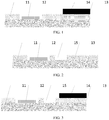
FIG. 1 , at least onesubstrate feature point 12 is arranged at a portion, which is not coated by asolder mask 13, on an upper surface of abase material 11 of the substrate. Generally, the substrate feature point 12 (Cu pad) has a thickness of 10 to 20 µm. Thesolder mask 13 on the upper surface of thebase material 11 of the substrate may project relative to the substrate feature point due to the thickness of the copper (Cu) foil. If anexhaust slot 14 is arranged in the vicinity of the substrate feature point 12., and when the epoxy resin molding compound in the vicinity of theexhaust slot 14 overflows, the overflowing epoxy resin molding compound may flow to the upper part of thesubstrate feature point 12 and covers thesubstrate feature point 12. - Covering the substrate feature point may severely affect the process precision and efficiency of the each stage in the subsequent process. If different molds and substrate feature points are designed for different products, product cost may be increased.
- In view of the above, the present application provides a substrate for chip package. With the substrate, the problem of covering the substrate feature point due to irregular flowing of a packaging material is prevented with no need to re-design a different mold and substrate feature point.
- The present application provides a substrate for chip package. A portion, which is not coated by a solder mask, on an upper surface of a base material of the substrate is provided with at least one substrate feature point. The upper surface of the base material of the substrate is provided with at least one slot. The slot is configured to guide an irregularly flowing packaging material in the course of chip packaging.
- As known from the above technical solution, at least one slot is arranged on the upper surface of the base material of the substrate according to the present application. The irregularly flowing packaging material in the course of chip packaging may be guided to the slot, such that the package material may not be randomly distributed. In this way, the normal appearance of the substrate is not affected, and the substrate feature point is covered. In addition, according to the present application, there is no need to re-design a different mold and substrate feature point, and thus product cost may not be increased.
- To more clearly describe technical solutions according to the embodiments of the present application or in the prior art, drawings that are to be referred for description of the embodiments or the prior art are briefly described hereinafter. Apparently, the drawings described hereinafter merely illustrate some embodiments of the present application. Persons of ordinary skill in the art may also derive other drawings based on the drawings described herein.
-
FIG. 1 is a schematic structural view of a substrate for chip package; -
FIG. 2 is a schematic view of a substrate for chip package according to some embodiments of the present application; -
FIG. 3 is a schematic view of a substrate for chip package according to some other embodiments of the present application;FIG. 4a and FIG. 4b are schematic views of a substrate for a chip package according to still some other embodiments of the present application. - According to the present application, at least one slot is arranged on the upper surface of the base material of the substrate. The irregularly flowing package material in the course of chip packaging may be guided to the slot, such that the package material may not be randomly distributed. In this way, the normal appearance of the substrate is not affected, and the substrate feature point is covered. In addition, according to the present application, there is no need to re-design a different mold and substrate feature point, and thus product cost may not be increased.
- Definitely, the implementation of any technical solution of the present application does not need to achieve all the above advantages.
- To make a person skilled in the art better understand the technical solutions of the present application, the technical solutions in the embodiments of the present application are described clearly and completely with reference to the accompanying drawings in the embodiments of the present application. Apparently, the described embodiments are merely some of rather than all of the embodiments of the present application. Based on the embodiments of the present application, all other embodiments derived by persons of ordinary skill in the art without any creative efforts shall fall within the protection scope of the present application.
- Specific implementations of the present application are further described hereinafter with reference to drawings of the present application.
- Referring to
FIG. 2 , one embodiment of the present application provides a substrate for chip package. At least onesubstrate feature point 12 is provided on a portion of an upper surface of thebase material 11 of the substrate which is not covered by asolder mask 13. At least oneslot 15 is arranged on the upper surface of thebase material 11 of the substrate. Theslot 15 is configured to guide an irregularly flowing package material in the course of chip packaging. - Specifically, the
substrate feature point 12 is an optical positioning point. - According to the present application, at least one
slot 15 is arranged on the upper surface of thebase material 11 of the substrate. The irregularly flowing package material in the course of chip packaging may be guided to theslot 15, such that the package material may not be randomly distributed. In this way, the normal appearance of the substrate is not affected, and the substrate feature point is covered. In addition, according to the present application, there is no need to re-design a different mold and substrate feature point, and thus product cost may not be increased. - Referring to
FIG. 3 , another embodiment of the present application provides a substrate for chip package. At least onesubstrate feature point 12 is arranged on an upper surface, which is not covered by asolder mask 13, of abase material 11 of the substrate. At least oneexhaust slot 14 is arranged on an upper surface of thesolder mask 13. At least oneslot 15 is arranged on the upper surface of thebase material 11 of the substrate. Theslot 15 is configured to guide an epoxy resin molding plastic overflowing from theexhaust slot 14. - Specifically, the
substrate feature point 12 is an optical positioning point. - According to the present application, at least one
slot 15 is arranged on the upper surface of thebase material 11 of the substrate. The epoxy resin overflowing from theexhaust slot 14 in the course of chip packaging may be guided to theslot 15, such that the epoxy resin may not be randomly distributed. In this way, the normal appearance of the substrate is not affected, and the substrate feature point is covered. In addition, according to the present application, there is no need to re-design a different mold and substrate feature point, and thus product cost may not be increased. - In one specific implementation of the present application, referring to
FIG. 4a and FIG. 4b , a distance from theslot 15 to theexhaust slot 14 is greater than or equal to 50 µm. - According to the present application, the
slot 15 is arranged in the vicinity of theslot 15, which achieves the effect of a guide slot. When the package material overflows, under different pressure intensities in the vicinity of theslot 15 and inside theslot 15, the overflowing package material may flow in accordance with the shape of theslot 15. In this way, the overflowing packaging material does not affect the appearance of the substrate. - In another specific implementation of the present application, referring to
FIG. 4a and FIG. 4b , a distance from theslot 15 to thesubstrate feature point 12 is greater than or equal to 100 µm. - According to the present application, the
slot 15 is arranged in the vicinity of thesubstrate feature point 12, which achieves the effect of a guide slot. When the packaging material overflows, under different pressure intensities in the vicinity of theslot 15 and inside theslot 15, the overflowing packaging material may flow in accordance with the shape of theslot 15. In this way, the overflowing packaging material does not affect the appearance of the substrate. - The shape of the
slot 15 is such defined that the substrate feature point is surrounded, such that the overflowing packaging material is further prevented from covering thesubstrate feature point 12. - In still another specific implementation of the present application, the shape of the
slot 15 is designed according to a space in which the slot is located. Therefore, according to an embodiment of the present application, the shape of theslot 15 may be defined according to the spaces in which thebase material 11 of the substrate, thesubstrate feature point 12 and theexhaust slot 14 are located. - In still another specific implementation of the present application, a depth of the
slot 15 is determined according to a thickness of thesolder mask 13 and a thickness of a cupper foil. If the thicknesses of thesolder mask 13 and the cupper foil are small, the depth of theslot 15 is also small; and if the thicknesses of thesolder mask 13 and the cupper foil are great, the depth of theslot 15 is great. - In still another specific implementation of the present application, the shape of the
substrate feature point 12 varies according to a dimension of theslot 15. The shape of thesubstrate feature point 12 is not fixed, and varies according to the dimension of theslot 15 on the upper surface of thebase material 11 of the substrate, such that the substrate feature point is not covered by the packaging material. - Although the preferred embodiments of the present application are described above, once knowing the basic creative concept, a person skilled in the art can make other modifications and variations to these embodiments. Therefore, the appended claims are intended to be construed as covering the preferred embodiments and all the modifications and variations falling within the scope of the present application. Obviously, a person skilled in the art can make various modifications and variations to the present application without departing from the spirit and scope of the present application. In this way, the present application is intended to cover the modifications and variations if they fall within the scope of the appended claims of the present application and equivalent technologies thereof.
Claims (9)
- A substrate for chip package, comprising a portion on an upper surface of a base material of the substrate, wherein the portion is uncovered by a solder mask, and is provided with at least one substrate feature point;
wherein the upper surface of the base material of the substrate is provided with at least one slot, the slot being configured to guide an irregularly flowing packaging material in a course of chip packaging. - The substrate for chip package according to claim 1, wherein an upper surface of the solder mask is provided with at least one exhaust slot, and the slot is configured to guide an epoxy resin molding plastic overflowing from the at least one exhaust slot.
- The substrate for chip package according to claim 2, wherein a distance from the slot to the at least one exhaust slot is greater than or equal to 50 µm.
- The substrate for chip package according to claim 1, wherein a distance from the slot to the substrate feature point is greater than or equal to 100 µm.
- The substrate for chip package according to claim 4, wherein the slot has a shape designed to surround the substrate feature point.
- The substrate for chip package according to claim 1, wherein the shape of the slot is designed based on a space in which the at least one slot is located.
- The substrate for chip package according to claim 1, wherein a depth of the slot is determined based on a thickness of the solder mask and a thickness of a copper foil.
- The substrate for chip package according to claim 1, wherein a shape of the substrate feature point varies based on a dimension of the slot.
- The substrate for chip package according to any one of claims 1 to 8, wherein the substrate feature point is an optical positioning point.
Applications Claiming Priority (1)
| Application Number | Priority Date | Filing Date | Title |
|---|---|---|---|
| PCT/CN2017/000030 WO2018126336A1 (en) | 2017-01-03 | 2017-01-03 | Substrate structure for packaging chip |
Publications (2)
| Publication Number | Publication Date |
|---|---|
| EP3419052A1 true EP3419052A1 (en) | 2018-12-26 |
| EP3419052A4 EP3419052A4 (en) | 2019-09-18 |
Family
ID=62788918
Family Applications (1)
| Application Number | Title | Priority Date | Filing Date |
|---|---|---|---|
| EP17889948.0A Withdrawn EP3419052A4 (en) | 2017-01-03 | 2017-01-03 | SUBSTRATE STRUCTURE FOR CHIP PACKAGING |
Country Status (4)
| Country | Link |
|---|---|
| US (1) | US20190013253A1 (en) |
| EP (1) | EP3419052A4 (en) |
| CN (1) | CN108886032A (en) |
| WO (1) | WO2018126336A1 (en) |
Family Cites Families (11)
| Publication number | Priority date | Publication date | Assignee | Title |
|---|---|---|---|---|
| TWI301315B (en) * | 2006-04-13 | 2008-09-21 | Advanced Semiconductor Eng | Substrate structure having solder mask layer and process for making the same |
| CN101281900B (en) * | 2007-04-04 | 2010-11-24 | 日月光半导体制造股份有限公司 | Systematic package with structure for preventing solder ball pad from being contaminated and manufacturing method thereof |
| JP5286893B2 (en) * | 2007-04-27 | 2013-09-11 | 日立化成株式会社 | Connection terminal, semiconductor package using connection terminal, and method of manufacturing semiconductor package |
| CN101609824B (en) * | 2008-06-18 | 2011-01-12 | 力成科技股份有限公司 | General-purpose substrate for semiconductor packaging and semiconductor package structure |
| JP4755225B2 (en) * | 2008-07-08 | 2011-08-24 | 力成科技股▲分▼有限公司 | Semiconductor package substrate and semiconductor package using the same |
| CN103021902A (en) * | 2011-09-21 | 2013-04-03 | 国碁电子(中山)有限公司 | Mould casting device and method for semiconductor package |
| US20140118978A1 (en) * | 2012-10-25 | 2014-05-01 | Po-Chun Lin | Package substrate and chip package using the same |
| CN103985645B (en) * | 2014-05-27 | 2017-02-15 | 无锡必创传感科技有限公司 | Semiconductor packaging piece and manufacturing method thereof |
| JP6387256B2 (en) * | 2014-07-07 | 2018-09-05 | ルネサスエレクトロニクス株式会社 | Manufacturing method of semiconductor device |
| US9520352B2 (en) * | 2014-12-10 | 2016-12-13 | Shinko Electric Industries Co., Ltd. | Wiring board and semiconductor device |
| JP2017021878A (en) * | 2015-07-13 | 2017-01-26 | 日東電工株式会社 | Suspension substrate assembly sheet with circuit, manufacturing method thereof, and inspection method thereof |
-
2017
- 2017-01-03 WO PCT/CN2017/000030 patent/WO2018126336A1/en not_active Ceased
- 2017-01-03 EP EP17889948.0A patent/EP3419052A4/en not_active Withdrawn
- 2017-01-03 CN CN201780005332.0A patent/CN108886032A/en active Pending
-
2018
- 2018-09-14 US US16/131,149 patent/US20190013253A1/en not_active Abandoned
Also Published As
| Publication number | Publication date |
|---|---|
| WO2018126336A1 (en) | 2018-07-12 |
| US20190013253A1 (en) | 2019-01-10 |
| EP3419052A4 (en) | 2019-09-18 |
| CN108886032A (en) | 2018-11-23 |
Similar Documents
| Publication | Publication Date | Title |
|---|---|---|
| US8487426B2 (en) | Semiconductor package with embedded die and manufacturing methods thereof | |
| US6444499B1 (en) | Method for fabricating a snapable multi-package array substrate, snapable multi-package array and snapable packaged electronic components | |
| US9583447B2 (en) | EMI shielding method of semiconductor packages | |
| US9589906B2 (en) | Semiconductor device package and method of manufacturing the same | |
| CN102479767A (en) | Semiconductor device package with electromagnetic shielding | |
| KR20170067472A (en) | Printed circuit board and electronic component package having the same | |
| KR20200073950A (en) | Semiconductor package and fabricating method thereof | |
| WO2018113574A1 (en) | Process method for mounting pre-encapsulated metal conductive three-dimensional packaging structure | |
| KR20160001169A (en) | semiconductor package including marking layer | |
| US20200027737A1 (en) | Plating interconnect for silicon chip | |
| KR20080069931A (en) | Chip Carrier Including Interlocking Structure | |
| US9814166B2 (en) | Method of manufacturing electronic package module | |
| US20260060089A1 (en) | Leadframe with varying thicknesses and method of manufacturing semiconductor packages | |
| US20190013253A1 (en) | Substrate for chip package | |
| US9648760B2 (en) | Substrate structure and manufacturing method thereof | |
| US9437492B2 (en) | Substrate for alternative semiconductor die configurations | |
| US5250842A (en) | Semiconductor devices using tab tape | |
| CN104051373B (en) | Heat dissipation structure and manufacturing method of semiconductor package | |
| KR101261483B1 (en) | Method for manufacturing semiconductor package | |
| IT202100017213A1 (en) | Process for manufacturing semiconductor devices and corresponding semiconductor device | |
| KR101685545B1 (en) | Multi die stacking method using Printed Circuit Board and semiconductor package employing it | |
| CN216905291U (en) | Sound conducting plate and microphone equipment | |
| TWI603440B (en) | Semiconductor heat sink device and package structure using the same | |
| JPH04215461A (en) | Package for semiconductor device | |
| TW200644262A (en) | Optoelectronic chip package and method for manufacturing the same |
Legal Events
| Date | Code | Title | Description |
|---|---|---|---|
| STAA | Information on the status of an ep patent application or granted ep patent |
Free format text: STATUS: THE INTERNATIONAL PUBLICATION HAS BEEN MADE |
|
| PUAI | Public reference made under article 153(3) epc to a published international application that has entered the european phase |
Free format text: ORIGINAL CODE: 0009012 |
|
| STAA | Information on the status of an ep patent application or granted ep patent |
Free format text: STATUS: REQUEST FOR EXAMINATION WAS MADE |
|
| 17P | Request for examination filed |
Effective date: 20180917 |
|
| AK | Designated contracting states |
Kind code of ref document: A1 Designated state(s): AL AT BE BG CH CY CZ DE DK EE ES FI FR GB GR HR HU IE IS IT LI LT LU LV MC MK MT NL NO PL PT RO RS SE SI SK SM TR |
|
| AX | Request for extension of the european patent |
Extension state: BA ME |
|
| A4 | Supplementary search report drawn up and despatched |
Effective date: 20190820 |
|
| RIC1 | Information provided on ipc code assigned before grant |
Ipc: H01L 21/56 20060101ALN20190813BHEP Ipc: H01L 23/544 20060101ALI20190813BHEP Ipc: H01L 23/488 20060101AFI20190813BHEP |
|
| DAV | Request for validation of the european patent (deleted) | ||
| DAX | Request for extension of the european patent (deleted) | ||
| STAA | Information on the status of an ep patent application or granted ep patent |
Free format text: STATUS: EXAMINATION IS IN PROGRESS |
|
| 17Q | First examination report despatched |
Effective date: 20200423 |
|
| STAA | Information on the status of an ep patent application or granted ep patent |
Free format text: STATUS: THE APPLICATION HAS BEEN WITHDRAWN |
|
| 18W | Application withdrawn |
Effective date: 20200724 |