EP3417540B1 - Electrical capacitor - Google Patents
Electrical capacitor Download PDFInfo
- Publication number
- EP3417540B1 EP3417540B1 EP16716534.9A EP16716534A EP3417540B1 EP 3417540 B1 EP3417540 B1 EP 3417540B1 EP 16716534 A EP16716534 A EP 16716534A EP 3417540 B1 EP3417540 B1 EP 3417540B1
- Authority
- EP
- European Patent Office
- Prior art keywords
- capacitor
- film
- ceramic layer
- glass ceramic
- module
- Prior art date
- Legal status (The legal status is an assumption and is not a legal conclusion. Google has not performed a legal analysis and makes no representation as to the accuracy of the status listed.)
- Active
Links
- 239000003990 capacitor Substances 0.000 title claims description 118
- 239000002241 glass-ceramic Substances 0.000 claims description 58
- 229910052751 metal Inorganic materials 0.000 claims description 25
- 239000002184 metal Substances 0.000 claims description 25
- 239000004743 Polypropylene Substances 0.000 claims description 11
- 230000005540 biological transmission Effects 0.000 claims description 11
- -1 polypropylene Polymers 0.000 claims description 11
- 229920001155 polypropylene Polymers 0.000 claims description 11
- 239000002985 plastic film Substances 0.000 claims description 7
- 229920006255 plastic film Polymers 0.000 claims description 7
- 238000009434 installation Methods 0.000 claims 2
- 239000010408 film Substances 0.000 description 33
- 239000004065 semiconductor Substances 0.000 description 27
- 239000011888 foil Substances 0.000 description 17
- 238000004804 winding Methods 0.000 description 7
- 239000011521 glass Substances 0.000 description 6
- 239000002131 composite material Substances 0.000 description 4
- 238000004519 manufacturing process Methods 0.000 description 4
- 238000001465 metallisation Methods 0.000 description 4
- 239000010409 thin film Substances 0.000 description 4
- 238000004378 air conditioning Methods 0.000 description 2
- 230000007547 defect Effects 0.000 description 2
- VYPSYNLAJGMNEJ-UHFFFAOYSA-N Silicium dioxide Chemical compound O=[Si]=O VYPSYNLAJGMNEJ-UHFFFAOYSA-N 0.000 description 1
- 229910000831 Steel Inorganic materials 0.000 description 1
- GWEVSGVZZGPLCZ-UHFFFAOYSA-N Titan oxide Chemical compound O=[Ti]=O GWEVSGVZZGPLCZ-UHFFFAOYSA-N 0.000 description 1
- RTAQQCXQSZGOHL-UHFFFAOYSA-N Titanium Chemical compound [Ti] RTAQQCXQSZGOHL-UHFFFAOYSA-N 0.000 description 1
- 229910052782 aluminium Inorganic materials 0.000 description 1
- XAGFODPZIPBFFR-UHFFFAOYSA-N aluminium Chemical compound [Al] XAGFODPZIPBFFR-UHFFFAOYSA-N 0.000 description 1
- 229910052454 barium strontium titanate Inorganic materials 0.000 description 1
- 229910002113 barium titanate Inorganic materials 0.000 description 1
- JRPBQTZRNDNNOP-UHFFFAOYSA-N barium titanate Chemical compound [Ba+2].[Ba+2].[O-][Ti]([O-])([O-])[O-] JRPBQTZRNDNNOP-UHFFFAOYSA-N 0.000 description 1
- 239000000919 ceramic Substances 0.000 description 1
- 238000005524 ceramic coating Methods 0.000 description 1
- 239000011248 coating agent Substances 0.000 description 1
- 238000000576 coating method Methods 0.000 description 1
- 230000002950 deficient Effects 0.000 description 1
- 230000001419 dependent effect Effects 0.000 description 1
- 230000000694 effects Effects 0.000 description 1
- 239000006112 glass ceramic composition Substances 0.000 description 1
- 230000003993 interaction Effects 0.000 description 1
- 229910052451 lead zirconate titanate Inorganic materials 0.000 description 1
- HFGPZNIAWCZYJU-UHFFFAOYSA-N lead zirconate titanate Chemical compound [O-2].[O-2].[O-2].[O-2].[O-2].[Ti+4].[Zr+4].[Pb+2] HFGPZNIAWCZYJU-UHFFFAOYSA-N 0.000 description 1
- 239000000463 material Substances 0.000 description 1
- 238000000034 method Methods 0.000 description 1
- TWNQGVIAIRXVLR-UHFFFAOYSA-N oxo(oxoalumanyloxy)alumane Chemical compound O=[Al]O[Al]=O TWNQGVIAIRXVLR-UHFFFAOYSA-N 0.000 description 1
- 239000002245 particle Substances 0.000 description 1
- 238000002360 preparation method Methods 0.000 description 1
- 229910052814 silicon oxide Inorganic materials 0.000 description 1
- 239000010959 steel Substances 0.000 description 1
- 238000003860 storage Methods 0.000 description 1
- 239000000758 substrate Substances 0.000 description 1
- 239000010936 titanium Substances 0.000 description 1
- 229910052719 titanium Inorganic materials 0.000 description 1
- OGIDPMRJRNCKJF-UHFFFAOYSA-N titanium oxide Inorganic materials [Ti]=O OGIDPMRJRNCKJF-UHFFFAOYSA-N 0.000 description 1
Images


Classifications
-
- H—ELECTRICITY
- H02—GENERATION; CONVERSION OR DISTRIBUTION OF ELECTRIC POWER
- H02M—APPARATUS FOR CONVERSION BETWEEN AC AND AC, BETWEEN AC AND DC, OR BETWEEN DC AND DC, AND FOR USE WITH MAINS OR SIMILAR POWER SUPPLY SYSTEMS; CONVERSION OF DC OR AC INPUT POWER INTO SURGE OUTPUT POWER; CONTROL OR REGULATION THEREOF
- H02M7/00—Conversion of ac power input into dc power output; Conversion of dc power input into ac power output
- H02M7/42—Conversion of dc power input into ac power output without possibility of reversal
- H02M7/44—Conversion of dc power input into ac power output without possibility of reversal by static converters
- H02M7/48—Conversion of dc power input into ac power output without possibility of reversal by static converters using discharge tubes with control electrode or semiconductor devices with control electrode
- H02M7/483—Converters with outputs that each can have more than two voltages levels
- H02M7/49—Combination of the output voltage waveforms of a plurality of converters
-
- H—ELECTRICITY
- H01—ELECTRIC ELEMENTS
- H01G—CAPACITORS; CAPACITORS, RECTIFIERS, DETECTORS, SWITCHING DEVICES OR LIGHT-SENSITIVE DEVICES, OF THE ELECTROLYTIC TYPE
- H01G4/00—Fixed capacitors; Processes of their manufacture
- H01G4/002—Details
- H01G4/018—Dielectrics
- H01G4/06—Solid dielectrics
-
- H—ELECTRICITY
- H01—ELECTRIC ELEMENTS
- H01G—CAPACITORS; CAPACITORS, RECTIFIERS, DETECTORS, SWITCHING DEVICES OR LIGHT-SENSITIVE DEVICES, OF THE ELECTROLYTIC TYPE
- H01G4/00—Fixed capacitors; Processes of their manufacture
- H01G4/002—Details
- H01G4/018—Dielectrics
- H01G4/06—Solid dielectrics
- H01G4/08—Inorganic dielectrics
- H01G4/12—Ceramic dielectrics
-
- H—ELECTRICITY
- H01—ELECTRIC ELEMENTS
- H01G—CAPACITORS; CAPACITORS, RECTIFIERS, DETECTORS, SWITCHING DEVICES OR LIGHT-SENSITIVE DEVICES, OF THE ELECTROLYTIC TYPE
- H01G4/00—Fixed capacitors; Processes of their manufacture
- H01G4/002—Details
- H01G4/018—Dielectrics
- H01G4/06—Solid dielectrics
- H01G4/14—Organic dielectrics
-
- H—ELECTRICITY
- H01—ELECTRIC ELEMENTS
- H01G—CAPACITORS; CAPACITORS, RECTIFIERS, DETECTORS, SWITCHING DEVICES OR LIGHT-SENSITIVE DEVICES, OF THE ELECTROLYTIC TYPE
- H01G4/00—Fixed capacitors; Processes of their manufacture
- H01G4/002—Details
- H01G4/018—Dielectrics
- H01G4/20—Dielectrics using combinations of dielectrics from more than one of groups H01G4/02 - H01G4/06
- H01G4/206—Dielectrics using combinations of dielectrics from more than one of groups H01G4/02 - H01G4/06 inorganic and synthetic material
-
- H—ELECTRICITY
- H02—GENERATION; CONVERSION OR DISTRIBUTION OF ELECTRIC POWER
- H02M—APPARATUS FOR CONVERSION BETWEEN AC AND AC, BETWEEN AC AND DC, OR BETWEEN DC AND DC, AND FOR USE WITH MAINS OR SIMILAR POWER SUPPLY SYSTEMS; CONVERSION OF DC OR AC INPUT POWER INTO SURGE OUTPUT POWER; CONTROL OR REGULATION THEREOF
- H02M7/00—Conversion of ac power input into dc power output; Conversion of dc power input into ac power output
- H02M7/42—Conversion of dc power input into ac power output without possibility of reversal
- H02M7/44—Conversion of dc power input into ac power output without possibility of reversal by static converters
- H02M7/48—Conversion of dc power input into ac power output without possibility of reversal by static converters using discharge tubes with control electrode or semiconductor devices with control electrode
- H02M7/483—Converters with outputs that each can have more than two voltages levels
Definitions
- the invention relates to a converter with a series connection of a plurality of modules, each of which has at least two electronic switching elements and an electrical capacitor.
- the electrical capacitor has a dielectric which has a foil.
- Such a capacitor is also referred to as a film capacitor.
- the film is often made of polypropylene.
- capacitors in which the size of the capacitors plays an important role include electrical power converters, in particular electrical power converters in offshore applications.
- VSC voltage sourced converter
- the Power converters can be easily adapted (scaled) to different voltages and a desired output voltage can be generated relatively precisely. These converters are often used in the high-voltage area, for example as converters in high-voltage direct current transmission systems or as reactive power compensators in flexible three-phase transmission systems.
- Such converters are often of considerable size. Depending on the area of application, the costs for the land or for the converted space of the converter can be considerable. Enclosed space is expensive, especially in the case of offshore systems. In addition, there may be costs for air conditioning, which can also increase with the size of the power converter.
- the electrical capacitor is often one of the largest components in the modules of such a converter. The capacitor therefore has a significant influence on the size of the individual modules and thus on the size of the converter.
- An example of such a converter is in DE 10 2013 214 693 A1 to find.
- the invention is based on the object of specifying a converter in which the capacitor (in relation to its electrical capacitance and its dielectric strength) has a small overall size.
- An electrical capacitor with a dielectric which has a (flexible) foil which is provided with a glass ceramic layer. It is a film capacitor. In the case of this capacitor, it is particularly advantageous that the film is provided with a glass ceramic layer.
- the glass ceramic has a higher dielectric constant ⁇ r (relative permittivity ⁇ r ) than, for example, polypropylene.
- ⁇ r relative permittivity
- this electrical capacitor can store a larger amount of electrical charge than a capacitor whose dielectric consists entirely of polypropylene.
- the capacitor can be made very compact and, compared with capacitors with a glass-ceramic-free dielectric, a smaller size is achieved.
- the capacitor is constructed in such a way that the glass ceramic layer has a thickness between 1 nm and 10 nm. Because of this small thickness, the glass ceramic layer is flexible and elastic, so that the glass ceramic layer can be wound up (rolled up) together with the film to form a film roll. This allows this capacitor to be implemented in a foil-wound design.
- the capacitor is also designed so that the film is a plastic film.
- the film, especially the plastic film forms a carrier film for the glass ceramic layer. Due to its mechanical stability, the plastic film enables the use of a very thin glass ceramic layer. This makes it easier to wind up the dielectric and enables the capacitor to have a small overall size.
- the capacitor can also be designed in such a way that the film is provided with a metal layer which forms an electrode of the capacitor or the glass ceramic layer is provided with a metal layer which forms an electrode of the capacitor.
- the metal layer can be applied directly to the film or to the glass ceramic layer as a metallization layer.
- Two foils provided in this way with the glass ceramic layer and the metal layer can then be wound up to form a foil roll of the capacitor in such a way that the two foils form adjacent layers of the foil roll. This creates a capacitor that has two metal layers and thus two electrodes.
- the foil provided with the glass ceramic layer and the metal layer is also referred to below as a capacitor strip.
- the capacitor can also be designed in such a way that one side of the foil (the first side of the foil) is provided with the glass ceramic layer and the opposite side of the foil (the second side of the foil) is provided with a further glass ceramic layer.
- the flexibility of the glass ceramic layers is not reduced (due to the unchanged thickness of the glass ceramic layers).
- the capacitor can also be designed such that the glass ceramic layer is provided with a metal layer that forms an electrode of the capacitor, or the further glass ceramic layer is provided with a metal layer that forms an electrode of the capacitor.
- the capacitor with the two electrodes can be implemented by winding two capacitor strips configured in this way into one another.
- the capacitor can also be designed in such a way that the film comprises polypropylene. It is therefore a polypropylene-containing plastic film, in particular a polypropylene film. Polypropylene is available inexpensively and is easy to process. In addition, polypropylene has the necessary mechanical strength to support the glass ceramic layer.
- the converter is also disclosed with the series connection of a plurality of modules, each of which has at least two electronic switching elements and a capacitor according to one of the variants described above.
- a high-voltage direct current transmission system with such a converter is also disclosed.
- a reactive power compensation system with such a converter is also disclosed.
- Such a converter such a high-voltage direct current transmission system and such a reactive power compensation system have advantages similar to those explained above in connection with the capacitor.
- the converter, the high-voltage direct current transmission system and the reactive power compensation system can be implemented with a comparatively small size.
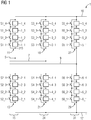
- FIG. 1 is a converter 1 in the form of a modular multilevel converter 1 (modular multilevel converter, MMC) shown.
- This multilevel converter 1 has a first AC voltage connection 5, a second AC voltage connection 7 and a third AC voltage connection 9.
- the first AC voltage connection 5 is electrically connected to a first phase module branch 11 and a second phase module branch 13.
- the first phase module branch 11 and the second phase module branch 13 form a first phase module 15 of the converter 1.
- the end of the first phase module branch 11 facing away from the first alternating voltage connection 5 is electrically connected to a first direct voltage connection 16; that end of the second phase module branch 13 facing away from the first AC voltage connection 5 is electrically connected to a second DC voltage connection 17.
- the first DC voltage connection 16 is a positive DC voltage connection; the second DC voltage connection 17 is a negative DC voltage connection.
- the second AC voltage connection 7 is electrically connected to one end of a third phase module branch 18 and to one end of a fourth phase module branch 21.
- the third phase module branch 18 and the fourth phase module branch 21 form a second phase module 24.
- the third AC voltage connection 9 is electrically connected to one end of a fifth phase module branch 27 and to one end of a sixth phase module branch 29.
- the fifth phase module branch 27 and the sixth phase module branch 29 form a third phase module 31.
- the end of the third phase module branch 18 facing away from the second alternating voltage connection 7 and the end of the fifth phase module branch 27 facing away from the third alternating voltage connection 9 are electrically connected to the first direct voltage connection 16.
- the end of the fourth phase module branch 21 facing away from the second alternating voltage connection 7 and the end of the sixth phase module branch 29 facing away from the third alternating voltage connection 9 are electrically connected to the second direct voltage connection 17.
- Each phase module branch has a plurality of modules (1_1, 1_2, 1_3, 1_4; 2_1 ... 2_4; etc.) which are electrically connected in series (by means of their galvanic power connections). Such modules are also referred to as submodules.
- each phase module branch has 4 modules (converter modules). The number of modules electrically connected in series (by means of their galvanic power connections) can be very different, at least three modules are connected in series, but 50, 100 or more modules can also be electrically connected in series, for example.
- a switch (bridging switch, bypass switch) is assigned to each module, which can bypass (short-circuit) the module (if the module is defective).
- a first switch S1_1 is assigned to the first module 1_1.
- the first switch S1_1 When a defect occurs in the first module 1_1, the first switch S1_1 is activated by a switch control device inside the module; the first switch S1_1 then closes; that is, the first switch S1_1 changes from the open switching state to the closed switching state.
- Each of the modules of the converter 1 is provided with a switch.
- a module 201 is shown as an example. This can be, for example, the module 1_1 of the first phase module branch 11 (or one of the others in FIG Figure 1 modules shown).
- the module is designed as a half-bridge module 201.
- the module 201 has a first semiconductor valve 202, which can be switched on and off, with a first diode 204 connected in anti-parallel.
- the module 201 has a second semiconductor valve 206 that can be switched on and off with a second diode 208 connected in anti-parallel, as well as an electrical energy store 210 in the form of a capacitor 210.
- the condenser 210 is a unipolar capacitor 210 (unipolar storage capacitor 210).
- the first turn-off semiconductor valve 202 is a first electronic switching element 202; the second turn-off semiconductor valve 206 is a second electronic switching element 206.
- the first turn-off semiconductor valve 202 and the second turn-off semiconductor valve 206 can each be configured as an IGBT (insulated-gate bipolar transistor).
- the first switch-off semiconductor valve 202 is electrically connected in series with the second switch-off semiconductor valve 206.
- a first galvanic module connection 212 is arranged at the connection point between the two semiconductor valves 202 and 206.
- a second galvanic module connection 215 is arranged at the connection of the second semiconductor valve 206, which is opposite the connection point.
- the second module connection 215 is also connected to a first connection of the energy store 210; a second connection of the energy store 210 is electrically connected to the connection of the first semiconductor valve 202, which is opposite the connection point.
- the energy store 210 is thus electrically connected in parallel to the series connection of the first semiconductor valve 202 and the second semiconductor valve 206.By appropriate control of the first semiconductor valve 202 and the second semiconductor valve 206 (for example by an internal module electronic control circuit) it can be achieved that between the first galvanic module connection 212 and the second galvanic module connection 215 either the voltage of the energy store 210 is output or no voltage is output (that is to say a zero voltage is output). By interaction of the modules of the individual phase module branches, the respective desired output voltage of the converter can be generated.
- FIG. 3 a further embodiment of a module 301 is shown.
- This module 301 can be, for example, module 1_2 (or one of the other modules shown in FIG. 1).
- first semiconductor valve 202, second semiconductor valve 206, first diode 204, second diode 208 and energy store 210 has the in Figure 3
- the module 301 shown has a third semiconductor valve 302 that can be switched on and off with a third diode 304 connected in anti-parallel, and a fourth semiconductor valve 306 that can be switched on and off with a fourth diode 308 connected in anti-parallel.
- the third switchable semiconductor valve 302 is a third electronic switching element 302; the fourth turn-off semiconductor valve 306 is a fourth electronic switching element 306.
- the third turn-off semiconductor valve 302 and the fourth turn-off semiconductor valve 306 can each be configured as an IGBT.
- the second galvanic module connection 315 is not electrically connected to the second semiconductor valve 206, but rather the second galvanic module connection 315 is electrically connected to a center point of an electrical series circuit comprising the third semiconductor valve 302 and the fourth semiconductor valve 306.
- the module 301 of the Figure 3 is a so-called full bridge module 301.
- This full bridge module 301 is characterized by the fact that, with appropriate control of the four semiconductor valves between the first galvanic module connection 212 and the second galvanic module connection 315, either the positive voltage of the energy store 210 or the negative voltage of the Energy store 210 or a voltage of the value zero (zero voltage) can be output.
- the polarity of the output voltage can thus be reversed by means of the full bridge module 301.
- the converter 1 can either have only half-bridge modules 201, only full-bridge modules 301 or also half-bridge modules 201 and full-bridge modules 301.
- the module can also be another module, for example a multilevel module that has several capacitors as energy stores, with the voltages of the capacitors being able to be combined in different ways.
- FIG. 4 an exemplary embodiment of a high-voltage direct current transmission system 401 is shown schematically.
- This high-voltage direct current transmission system 401 has two converters 1 according to FIG Figure 1 on. These two converters 1 are electrically connected to one another on the DC voltage side via a high-voltage DC connection 405.
- the two positive DC voltage connections 16 of the converters 1 are electrically connected to one another by means of a first high-voltage DC line 405a; the two negative direct voltage connections 17 of the two converters 1 are electrically connected to one another by means of a second high-voltage direct current line 405b.
- electrical energy can be transmitted over long distances; the high-voltage direct current connection 405 then has a corresponding length.
- FIG. 5 an embodiment of a power converter 501 is shown, which serves as a reactive power compensator 501.
- This converter 501 only has the three phase module branches 11, 18 and 27, which form three phase modules 505, 507 and 509 of the converter.
- the number of phase modules 505, 507 and 509 corresponds to the number of phases of an AC voltage network 511 to which the converter 501 is connected.
- the three phase module branches 11, 18 and 27 are connected to one another in a star shape.
- the end of the three phase module branches opposite the star point is electrically connected to a phase line 515, 517 and 519 of the three-phase AC voltage network 511.
- the three phase modules 505, In another exemplary embodiment, 507 and 509 can also be connected in a delta connection instead of in a star connection.
- FIG 6 an embodiment of a capacitor strip 601 of an electrical capacitor is shown schematically.
- This electrical capacitor is a film capacitor.
- This electrical capacitor is, for example, the one in the Figures 2 and 3 illustrated capacitor 210 of the module of the converter.
- Figure 6 shows a sectional view of a section from the capacitor strip (in the developed state).
- the capacitor strip 601 of the film capacitor has a film 603 to which a glass ceramic layer 606 is applied.
- the film 603 is a carrier film 603 for the glass ceramic layer 606.
- the film 603 and the glass ceramic layer 606 form a dielectric 610 of the capacitor.
- the film 603 and the glass ceramic layer 606 form a composite. This composite represents the dielectric 610 of the capacitor.
- the film 603 is provided (on one side) with a metal layer 613 (metallization layer 613).
- the metal layer 613 forms an electrode of the capacitor.
- the film 603 is a plastic film 603, preferably a polypropylene film 603.
- This plastic film 603 is provided with the glass ceramic layer 606 (glass ceramic coating 606).
- the glass ceramic layer 606 as a coating on the film 603 is advantageous because this results in a relatively elastic composite or composite material which can be wound up. As a result, the brittleness of the glass ceramic as such is not disadvantageous in the manufacture of the capacitor.
- Such a glass ceramic can, for example, have titanates or oxides, in particular titanium oxide, Silicon oxide, aluminum oxide, barium titanate or barium strontium titanate.
- the glass ceramic can have ceramic particles which are encased by glass.
- two capacitor strips are used in accordance with Figure 6 wound up together to form a common roll (foil roll). This is done in such a way that the two capacitor strips form adjacent layers of the coil.
- FIG. 7 a section of such a winding with two capacitor strips is shown.
- the first capacitor strip 601 is shown, which consists of the film 603, the glass ceramic layer 606 and the metal layer 613.
- a second capacitor strip is shown, which consists of a second film 703, a second glass ceramic layer 706 and a second metal layer 713.
- the metal layer 613 forms the first electrode of the capacitor; the second metal layer 713 forms the second electrode of the capacitor.
- FIG. 7 thus shows a section from the capacitor, in particular a section from the capacitor 210 of FIG Figures 2 and 3 .
- FIG Figure 8 a further exemplary embodiment of a section from a capacitor strip 801 is shown.
- This capacitor strip 801 has the film 603 with the glass ceramic layer 606.
- a metal layer 813 (metallization layer 813) is applied to the glass ceramic layer 606.
- the film 603 and the glass ceramic layer 606 form the dielectric 610.
- the exemplary embodiment in FIG Figure 8 differs from the embodiment of Figure 6 only in that the metal layer is not applied to the foil 603, but to the glass ceramic layer 606.
- FIG. 9 a further embodiment of a capacitor strip 901 of the capacitor is shown.
- This capacitor strip 901 has the film 603.
- a first side 904 of the film 603 is provided with a first glass ceramic layer 906.
- a second side 908 of the film 603 (the second side 908 opposite the first side 904) is provided with a second glass ceramic layer 912.
- the film 603 is thus provided with a glass ceramic layer on both sides: with the first glass ceramic layer 906 and the second glass ceramic layer 912.
- the second glass ceramic layer 912 has a metal layer 915 (metallization layer 915) which forms an electrode of the capacitor.
- the film 603 with the first glass ceramic layer 906 and the second glass ceramic layer 912 form a dielectric 910 of the capacitor.
- FIG. 10 a further embodiment of a capacitor strip 1001 of the capacitor is shown.
- This capacitor strip 1001 differs from the capacitor strip 901 of FIG Figure 9 only in that the second glass ceramic layer 912 is not provided with a metal layer (metal layer-free second glass ceramic layer 912) and that the first glass ceramic layer 906 is provided with a metal layer 1015.
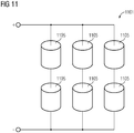
- FIG. 11 an embodiment of a capacitor 1101 is shown.
- the capacitor 1101 has a plurality of windings 1105 (foil windings 1105) which are partly connected electrically in series and partly connected electrically in parallel.
- windings 1105 foil windings 1105
- two of the coils are electrically connected in series.
- Three of these series connections are electrically connected in parallel.
- a capacitor can also consist only of series-connected windings, of parallel-connected windings, or only one winding.
- the capacitors described have a number of advantages. Due to the use of the glass ceramic layer, they have a relatively high temperature resistance, so less effort is required for air conditioning and the The service life of the capacitors is extended. Because of the glass ceramic layer with the relatively large relative permittivity ⁇ r , little foil area (little capacitor area) is required in order to realize a given electrical capacitance. This enables the capacitors to have a compact design, and these capacitors have a small overall size.
- An electrical capacitor has been described which is small in size in relation to its electrical capacitance. With this electrical capacitor, a power converter is built which has a small overall size. With this electrical capacitor, in particular high-voltage direct current transmission systems or reactive power compensation systems can be built, which also have a small overall size. As a result, the space required for capacitors, converters and the systems mentioned can be kept small, which can lead to considerable cost advantages (especially in the case of offshore applications).
Description
Die Erfindung betrifft einen Stromrichter mit einer Reihenschaltung aus einer Vielzahl von Modulen, welche jeweils mindestens zwei elektronische Schaltelemente und einen elektrischen Kondensator aufweisen. Der elektrische Kondensator hat ein Dielektrikum, das eine Folie aufweist.The invention relates to a converter with a series connection of a plurality of modules, each of which has at least two electronic switching elements and an electrical capacitor. The electrical capacitor has a dielectric which has a foil.
Ein solcher Kondensator wird auch als Folienkondensator bezeichnet. Oftmals besteht die Folie aus Polypropylen. Je größer die benötigte elektrische Kapazität des Kondensators ist und je größer die benötigte Spannungsfestigkeit des Kondensators ist, desto größer ist auch der Kondensator, d.h. desto größer ist das Volumen und damit die Baugröße des Kondensators. Es gibt Anwendungsfälle für Kondensatoren, bei denen die Baugröße der Kondensatoren eine bedeutende Rolle spielt. Zu diesen Anwendungsfällen gehören elektrische Stromrichter, insbesondere elektrische Stromrichter bei Offshore-Anwendungen.Such a capacitor is also referred to as a film capacitor. The film is often made of polypropylene. The larger the required electrical capacitance of the capacitor and the larger the required dielectric strength of the capacitor, the larger the capacitor, i.e. the larger the volume and thus the size of the capacitor. There are applications for capacitors in which the size of the capacitors plays an important role. These use cases include electrical power converters, in particular electrical power converters in offshore applications.
Stromrichter (power converter) sind leistungselektronische Schaltungen zum Umwandeln von elektrischer Energie. Mit Stromrichtern kann Wechselstrom in Gleichstrom, Gleichstrom in Wechselstrom, Wechselstrom in Wechselstrom anderer Frequenz und/oder Amplitude oder Gleichstrom in Gleichstrom anderer Spannungshöhe umgewandelt werden. Stromrichter können eine Vielzahl von gleichartigen Modulen (die auch als Submodule bezeichnet werden) aufweisen, welche elektrisch in Reihe geschaltet sind. Diese Module weisen jeweils mindestens zwei elektronische Schaltelemente und einen elektrischen Energiespeicher in Form eines elektrischen Kondensators auf. Solche Stromrichter werden als modulare Multilevelstromrichter bezeichnet und gehören zu den VSC-Stromrichtern (VSC = voltage sourced converter). Durch die elektrische Reihenschaltung der Module lassen sich hohe Ausgangsspannungen erreichen. Die Stromrichter sind einfach an unterschiedliche Spannungen anpassbar (skalierbar) und eine gewünschte Ausgangsspannung kann relativ genau erzeugt werden. Diese Stromrichter werden oftmals im Hochspannungsbereich eingesetzt, beispielsweise als Stromrichter bei Hochspannungs-Gleichstrom-Übertragungsanlagen oder als Blindleistungskompensatoren bei flexiblen Drehstromübertragungssystemen.Power converters are power electronic circuits for converting electrical energy. Converters can be used to convert alternating current into direct current, direct current into alternating current, alternating current into alternating current with a different frequency and / or amplitude, or direct current into direct current with a different voltage level. Power converters can have a large number of modules of the same type (which are also referred to as submodules), which are electrically connected in series. These modules each have at least two electronic switching elements and an electrical energy store in the form of an electrical capacitor. Such converters are called modular multilevel converters and belong to the VSC converters (VSC = voltage sourced converter). The electrical series connection of the modules enables high output voltages to be achieved. the Power converters can be easily adapted (scaled) to different voltages and a desired output voltage can be generated relatively precisely. These converters are often used in the high-voltage area, for example as converters in high-voltage direct current transmission systems or as reactive power compensators in flexible three-phase transmission systems.
Solche Stromrichter weisen oftmals eine beträchtliche Größe auf. Abhängig vom Einsatzgebiet können die Kosten für den Grund und Boden bzw. für den umbauten Raum der Stromrichter erheblich sein. Insbesondere bei Offshore-Anlagen ist umbauter Raum teuer. Dazu kommen ggf. noch Kosten für die Klimatisierung, die auch mit der Größe der Stromrichter ansteigen können. Der elektrische Kondensator ist oftmals eines der größten Bauelemente in den Modulen eines solchen Stromrichters. Daher hat der Kondensator einen wesentlichen Einfluss auf die Größe der einzelnen Module und damit auf die Größe des Stromrichters. Ein Beispiel solcher Stromrichter ist in der
Aus der Schrift "
Aus der Schrift "
Der Erfindung liegt die Aufgabe zugrunde, einen Stromrichter anzugeben, bei dem der Kondensator (bezogen auf seine elektrische Kapazität und seine Spannungsfestigkeit) eine geringe Baugröße aufweist.The invention is based on the object of specifying a converter in which the capacitor (in relation to its electrical capacitance and its dielectric strength) has a small overall size.
Diese Aufgabe wird erfindungsgemäß gelöst durch einen Stromrichter nach dem unabhängigen Patentanspruch. Vorteilhafte Ausführungsformen des Stromrichters sind in den abhängigen Patentansprüchen angegeben.This object is achieved according to the invention by a power converter according to the independent patent claim. Advantageous embodiments of the converter are specified in the dependent claims.
Offenbart wird ein elektrischer Kondensator mit einem Dielektrikum, das eine (flexible) Folie aufweist, die mit einer Glaskeramikschicht versehen ist. Es handelt sich dabei um einen Folienkondensator. Bei diesem Kondensator ist besonders vorteilhaft, dass die Folie mit einer Glaskeramikschicht versehen ist. Die Glaskeramik weist eine größere Dielektrizitätszahl εr (relative Permittivität εr) auf als beispielsweise Polypropylen. Dadurch kann dieser elektrische Kondensator eine größere elektrische Ladungsmenge speichern als ein Kondensator, dessen Dielektrikum vollständig aus Polypropylen besteht. Dadurch kann der Kondensator sehr kompakt aufgebaut werden und im Vergleich mit Kondensatoren mit einem glaskeramikfreien Dielektrikum wird eine geringere Baugröße erreicht. Der Kondensator ist so aufgebaut, dass die Glaskeramikschicht eine Dicke zwischen 1 nm und 10 nm aufweist. Aufgrund dieser geringen Dicke ist die Glaskeramikschicht flexibel und elastisch, so dass die Glaskeramikschicht zusammen mit der Folie aufgewickelt (aufgerollt) werden kann unter Bildung eines Folienwickels. Dadurch lässt sich dieser Kondensator in Folienwickel-Bauform realisieren.An electrical capacitor with a dielectric is disclosed which has a (flexible) foil which is provided with a glass ceramic layer. It is a film capacitor. In the case of this capacitor, it is particularly advantageous that the film is provided with a glass ceramic layer. The glass ceramic has a higher dielectric constant ε r (relative permittivity ε r ) than, for example, polypropylene. As a result, this electrical capacitor can store a larger amount of electrical charge than a capacitor whose dielectric consists entirely of polypropylene. As a result, the capacitor can be made very compact and, compared with capacitors with a glass-ceramic-free dielectric, a smaller size is achieved. The capacitor is constructed in such a way that the glass ceramic layer has a thickness between 1 nm and 10 nm. Because of this small thickness, the glass ceramic layer is flexible and elastic, so that the glass ceramic layer can be wound up (rolled up) together with the film to form a film roll. This allows this capacitor to be implemented in a foil-wound design.
Der Kondensator ist auch so ausgestaltet, dass die Folie eine Kunststofffolie ist. Die Folie, insbesondere die Kunststofffolie, bildet eine Trägerfolie für die Glaskeramikschicht. Durch ihre mechanische Stabilität ermöglicht die Kunststofffolie die Verwendung von einer sehr dünnen Glaskeramikschicht. Dadurch wird das Aufwickeln des Dielektrikums erleichtert und es wird eine geringe Baugröße des Kondensators ermöglicht.The capacitor is also designed so that the film is a plastic film. The film, especially the plastic film, forms a carrier film for the glass ceramic layer. Due to its mechanical stability, the plastic film enables the use of a very thin glass ceramic layer. This makes it easier to wind up the dielectric and enables the capacitor to have a small overall size.
Der Kondensator kann auch so ausgestaltet sein, dass die Folie mit einer Metallschicht versehen ist, die eine Elektrode des Kondensators bildet oder die Glaskeramikschicht mit einer Metallschicht versehen ist, die eine Elektrode des Kondensators bildet. Die Metallschicht kann dabei als eine Metallisierungsschicht unmittelbar auf die Folie oder auf die Glaskeramikschicht aufgebracht sein. Zwei derartig mit der Glaskeramikschicht und der Metallschicht versehene Folien können dann derart zu einem Folienwickel des Kondensators aufgewickelt werden, dass die beiden Folien benachbarte Lagen des Folienwickels bilden. Somit entsteht ein Kondensator, der zwei Metallschichten und damit zwei Elektroden aufweist. (Die mit der Glaskeramikschicht und der Metallschicht versehene Folie wird im Folgenden auch als Kondensatorstreifen bezeichnet.)The capacitor can also be designed in such a way that the film is provided with a metal layer which forms an electrode of the capacitor or the glass ceramic layer is provided with a metal layer which forms an electrode of the capacitor. The metal layer can be applied directly to the film or to the glass ceramic layer as a metallization layer. Two foils provided in this way with the glass ceramic layer and the metal layer can then be wound up to form a foil roll of the capacitor in such a way that the two foils form adjacent layers of the foil roll. This creates a capacitor that has two metal layers and thus two electrodes. (The foil provided with the glass ceramic layer and the metal layer is also referred to below as a capacitor strip.)
Der Kondensator kann auch so ausgestaltet sein, dass eine Seite der Folie (die erste Seite der Folie) mit der Glaskeramikschicht versehen ist und die gegenüberliegende Seite der Folie (die zweite Seite der Folie) mit einer weiteren Glaskeramikschicht versehen ist. Dies erlaubt es vorteilhafter Weise, bei unveränderter Dicke der Glaskeramikschichten zwischen zwei Elektroden des Kondensators die doppelte Menge an Glaskeramikmaterial anzuordnen. Dadurch lassen sich bei diesem Kondensator besonders große elektrische Kapazitäten pro Volumeneinheit erreichen. Dabei ist (aufgrund der unveränderten Dicke der Glaskeramikschichten) die Flexibilität der Glaskeramikschichten nicht verringert.The capacitor can also be designed in such a way that one side of the foil (the first side of the foil) is provided with the glass ceramic layer and the opposite side of the foil (the second side of the foil) is provided with a further glass ceramic layer. This advantageously allows twice the amount of glass ceramic material to be arranged between two electrodes of the capacitor with the thickness of the glass ceramic layers unchanged. In this way, particularly large electrical capacitances per unit volume can be achieved with this capacitor. The flexibility of the glass ceramic layers is not reduced (due to the unchanged thickness of the glass ceramic layers).
Der Kondensator kann auch so ausgestaltet sein, dass die Glaskeramikschicht mit einer Metallschicht versehen ist, die eine Elektrode des Kondensators bildet, oder die weitere Glaskeramikschicht mit einer Metallschicht versehen ist, die eine Elektrode des Kondensators bildet. Durch Ineinanderwickeln von zwei derartig ausgestalteten Kondensatorstreifen lässt sich der Kondensator mit den beiden Elektroden realisieren.The capacitor can also be designed such that the glass ceramic layer is provided with a metal layer that forms an electrode of the capacitor, or the further glass ceramic layer is provided with a metal layer that forms an electrode of the capacitor. The capacitor with the two electrodes can be implemented by winding two capacitor strips configured in this way into one another.
Der Kondensator kann auch so ausgestaltet sein, dass die Folie Polypropylen aufweist. Es handelt sich also um eine polypropylenhaltige Kunststofffolie, insbesondere um eine Polypropylenfolie. Polypropylen ist kostengünstig verfügbar und lässt sich gut verarbeiten. Außerdem weist Polypropylen die nötige mechanische Festigkeit auf, um die Glaskeramikschicht zu tragen.The capacitor can also be designed in such a way that the film comprises polypropylene. It is therefore a polypropylene-containing plastic film, in particular a polypropylene film. Polypropylene is available inexpensively and is easy to process. In addition, polypropylene has the necessary mechanical strength to support the glass ceramic layer.
Offenbart wird weiterhin der Stromrichter mit der Reihenschaltung aus einer Vielzahl von Modulen, welche jeweils mindestens zwei elektronische Schaltelemente und einen Kondensator nach einer der vorstehend beschriebenen Varianten aufweisen.The converter is also disclosed with the series connection of a plurality of modules, each of which has at least two electronic switching elements and a capacitor according to one of the variants described above.
Offenbart wird weiterhin eine Hochspannungs-Gleichstrom-Übertragungsanlage mit einem solchen Stromrichter.A high-voltage direct current transmission system with such a converter is also disclosed.
Offenbart wird weiterhin eine Blindleistungskompensationsanlage mit einem solchen Stromrichter.A reactive power compensation system with such a converter is also disclosed.
Ein derartiger Stromrichter, eine derartige Hochspannungs-Gleichstrom-Übertragungsanlage und eine derartige Blindleistungskompensationsanlage weisen ähnliche Vorteile auf, wie sie oben im Zusammenhang mit dem Kondensator erläutert worden sind. Insbesondere lassen sich der Stromrichter, die Hochspannungs-Gleichstrom-Übertragungsanlage und die Blindleistungskompensationsanlage mit einer vergleichsweise geringen Baugröße realisieren.Such a converter, such a high-voltage direct current transmission system and such a reactive power compensation system have advantages similar to those explained above in connection with the capacitor. In particular, the converter, the high-voltage direct current transmission system and the reactive power compensation system can be implemented with a comparatively small size.
Im Folgenden wird die Erfindung anhand von Ausführungsbeispielen näher erläutert. Gleiche Bezugszeichen verweisen dabei auf gleiche oder gleich wirkende Elemente. Dazu ist in
Figur 1- ein Ausführungsbeispiel eines modularen Multilevelstromrichters, in
Figur 2- ein Ausführungsbeispiel eines Moduls des Multilevelstromrichters, in
Figur 3- ein weiteres Ausführungsbeispiel eines Moduls, in
Figur 4- ein Ausführungsbeispiel einer Hochspannungs-Gleichstrom-Übertragungsanlage, in
Figur 5- ein Ausführungsbeispiel einer Blindleistungskompensationsanlage, in
Figur 6- eine schematische Darstellung eines Ausführungsbeispiels eines Kondensatorstreifens eines Kondensators, in
Figur 7- eine schematische Darstellung eines Ausführungsbeispiels zweier Kondensatorstreifen eines Kondensators, in
- Figur 8
- eine schematische Darstellung eines weiteren Ausführungsbeispiels eines Kondensatorstreifens eines Kondensators, in
- Figur 9
- eine schematische Darstellung eines weiteren Ausführungsbeispiels eines Kondensatorstreifens eines Kondensators, in
- Figur 10
- eine schematische Darstellung eines weiteren Ausführungsbeispiels eines Kondensatorstreifens eines Kondensators und in
Figur 11- ein Ausführungsbeispiel einer Zusammenschaltung von mehreren Kondensatoren dargestellt.
- Figure 1
- an embodiment of a modular multilevel converter, in
- Figure 2
- an embodiment of a module of the multilevel converter, in
- Figure 3
- another embodiment of a module, in
- Figure 4
- an embodiment of a high-voltage direct current transmission system, in
- Figure 5
- an embodiment of a reactive power compensation system, in
- Figure 6
- a schematic representation of an embodiment of a capacitor strip of a capacitor, in
- Figure 7
- a schematic representation of an embodiment of two capacitor strips of a capacitor, in
- Figure 8
- a schematic representation of a further embodiment of a capacitor strip of a capacitor, in
- Figure 9
- a schematic representation of a further embodiment of a capacitor strip of a capacitor, in
- Figure 10
- a schematic representation of a further embodiment of a capacitor strip of a capacitor and in
- Figure 11
- an embodiment of an interconnection of several capacitors is shown.
In
Der zweite Wechselspannungsanschluss 7 ist mit einem Ende eines dritten Phasenmodulzweigs 18 und mit einem Ende eines vierten Phasenmodulzweigs 21 elektrisch verbunden. Der dritte Phasenmodulzweig 18 und der vierte Phasenmodulzweig 21 bilden ein zweites Phasenmodul 24. Der dritte Wechselspannungsanschluss 9 ist mit einem Ende eines fünften Phasenmodulzweigs 27 und mit einem Ende eines sechsten Phasenmodulzweigs 29 elektrisch verbunden. Der fünfte Phasenmodulzweig 27 und der sechste Phasenmodulzweig 29 bilden ein drittes Phasenmodul 31.The second
Das dem zweiten Wechselspannungsanschluss 7 abgewandte Ende des dritten Phasenmodulzweigs 18 und das dem dritten Wechselspannungsanschluss 9 abgewandte Ende des fünften Phasenmodulzweigs 27 sind mit dem ersten Gleichspannungsanschluss 16 elektrisch verbunden. Das dem zweiten Wechselspannungsanschluss 7 abgewandte Ende des vierten Phasenmodulzweigs 21 und das dem dritten Wechselspannungsanschluss 9 abgewandte Ende des sechsten Phasenmodulzweigs 29 sind mit dem zweiten Gleichspannungsanschluss 17 elektrisch verbunden.The end of the third
Jeder Phasenmodulzweig weist eine Mehrzahl von Modulen (1_1, 1_2, 1_3, 1_4; 2_1 ... 2_4; usw.) auf, welche (mittels ihrer galvanischen Stromanschlüsse) elektrisch in Reihe geschaltet sind. Solche Module werden auch als Submodule bezeichnet. Im Ausführungsbeispiel der
Jedem Modul ist ein Schalter (Überbrückungsschalter, Bypassschalter) zugeordnet, der das Modul (bei einem Defekt des Moduls) überbrücken (kurzschließen) kann. Beispielsweise ist dem ersten Modul 1_1 ein erster Schalter S1_1 zugeordnet. Der erste Schalter S1_1 wird bei Auftreten eines Defekts an dem ersten Modul 1_1 von einer modulinternen Schalter-Ansteuereinrichtung angesteuert, daraufhin schließt der erste Schalter S1_1; das heißt, der erste Schalter S1_1 geht von dem geöffneten Schaltzustand in den geschlossenen Schaltzustand über. Jedes der Module des Stromrichters 1 ist mit einem Schalter versehen.A switch (bridging switch, bypass switch) is assigned to each module, which can bypass (short-circuit) the module (if the module is defective). For example, a first switch S1_1 is assigned to the first module 1_1. When a defect occurs in the first module 1_1, the first switch S1_1 is activated by a switch control device inside the module; the first switch S1_1 then closes; that is, the first switch S1_1 changes from the open switching state to the closed switching state. Each of the modules of the
In
Das erste abschaltbare Halbleiterventil 202 ist ein erstes elektronisches Schaltelement 202; das zweite abschaltbare Halbleiterventil 206 ist ein zweites elektronisches Schaltelement 206. Das erste abschaltbare Halbleiterventil 202 und das zweite abschaltbare Halbleiterventil 206 kann jeweils als ein IGBT (insulated-gate bipolar transistor) ausgestaltet sein. Das erste abschaltbare Halbleiterventil 202 ist elektrisch in Reihe geschaltet mit dem zweiten abschaltbaren Halbleiterventil 206. Am Verbindungspunkt zwischen den beiden Halbleiterventilen 202 und 206 ist ein erster galvanischer Modulanschluss 212 angeordnet. An dem Anschluss des zweiten Halbleiterventils 206, welcher dem Verbindungspunkt gegenüberliegt, ist ein zweiter galvanischer Modulanschluss 215 angeordnet. Der zweite Modulanschluss 215 ist weiterhin mit einem ersten Anschluss des Energiespeichers 210 verbunden; ein zweiter Anschluss des Energiespeichers 210 ist elektrisch verbunden mit dem Anschluss des ersten Halbleiterventils 202, der dem Verbindungspunkt gegenüberliegt.The first turn-off semiconductor valve 202 is a first electronic switching element 202; the second turn-off
Der Energiespeicher 210 ist also elektrisch parallel geschaltet zu der Reihenschaltung aus dem ersten Halbleiterventil 202 und dem zweiten Halbleiterventil 206. Durch entsprechende Ansteuerung des ersten Halbleiterventils 202 und des zweiten Halbleiterventils 206 (zum Beispiel durch eine modulinterne elektronische Ansteuerschaltung) kann erreicht werden, dass zwischen dem ersten galvanischen Modulanschluss 212 und dem zweiten galvanischen Modulanschluss 215 entweder die Spannung des Energiespeichers 210 ausgegeben wird oder keine Spannung ausgegeben wird (das heißt eine Nullspannung ausgegeben wird). Durch Zusammenwirken der Module der einzelnen Phasenmodulzweige kann so die jeweils gewünschte Ausgangsspannung des Stromrichters erzeugt werden.The
In
Das Modul 301 der
In
In
Die drei Phasenmodulzweige 11, 18 und 27 sind sternförmig miteinander verbunden. Das dem Sternpunkt entgegengesetzte Ende der drei Phasenmodulzweige ist mit jeweils einer Phasenleitung 515, 517 und 519 des dreiphasigen Wechselspannungsnetzes 511 elektrisch verbunden. (Die drei Phasenmodule 505, 507 und 509 können in einem anderen Ausführungsbeispiel anstelle in Sternschaltung auch in Dreieckschaltung geschaltet sein.) Der Stromrichter 501 kann das Wechselspannungsnetz 511 mit Blindleistung versorgen oder Blindleistung aus dem Wechselspannungsnetz 511 entnehmen.The three
In
Der Kondensatorstreifen 601 des Folienkondensators weist eine Folie 603 auf, auf die eine Glaskeramikschicht 606 aufgebracht ist. Die Folie 603 ist dabei eine Trägerfolie 603 für die Glaskeramikschicht 606. Die Folie 603 und die Glaskeramikschicht 606 bilden ein Dielektrikum 610 des Kondensators. Dabei bilden die Folie 603 und die Glaskeramikschicht 606 einen Verbundstoff. Dieser Verbundstoff stellt das Dielektrikum 610 des Kondensators dar. Die Folie 603 ist (einseitig) mit einer Metallschicht 613 (Metallisierungsschicht 613) versehen. Die Metallschicht 613 bildet eine Elektrode des Kondensators.The
Die Folie 603 ist eine Kunststofffolie 603, vorzugsweise eine Polypropylenfolie 603. Diese Kunststofffolie 603 ist mit der Glaskeramikschicht 606 (Glaskeramikbeschichtung 606) versehen. Die Glaskeramikschicht 606 als Beschichtung auf der Folie 603 ist deshalb vorteilhaft, weil sich dadurch ein relativ elastischer Verbundstoff bzw. Verbundwerkstoff ergibt, welcher aufgewickelt werden kann. Dadurch ist die Sprödigkeit der Glaskeramik als solche nicht nachteilig bei der Herstellung des Kondensators. Eine solche Glaskeramik kann beispielsweise Titanate oder Oxide aufweisen, insbesondere Titanoxid, Siliziumoxid, Aluminiumoxid, Bariumtitanat oder Barium-Strontium-Titanat. Die Glaskeramik kann keramische Partikel, die von Glas umhüllt sind, aufweisen.The
Bei der Herstellung des Kondensators werden zwei Kondensatorstreifen gemäß
In
In
In
In
In
Die beschriebenen Kondensatoren weisen eine Reihe von Vorteilen auf. Aufgrund der Verwendung der Glaskeramikschicht weisen sie eine relativ hohe Temperaturfestigkeit auf, daher werden weniger Aufwände zur Klimatisierung benötigt und die Lebensdauer der Kondensatoren wird verlängert. Aufgrund der Glaskeramikschicht mit der relativ großen relativen Permittivität εr wird wenig Folienfläche (wenig Kondensatorfläche) benötigt, um eine vorgegebene elektrische Kapazität zu realisieren. Dadurch lässt sich ein kompakter Aufbau der Kondensatoren realisieren und diese Kondensatoren weisen eine geringe Baugröße auf.The capacitors described have a number of advantages. Due to the use of the glass ceramic layer, they have a relatively high temperature resistance, so less effort is required for air conditioning and the The service life of the capacitors is extended. Because of the glass ceramic layer with the relatively large relative permittivity ε r , little foil area (little capacitor area) is required in order to realize a given electrical capacitance. This enables the capacitors to have a compact design, and these capacitors have a small overall size.
Es wurde ein elektrischer Kondensator beschrieben, welcher bezogen auf seine elektrische Kapazität eine geringe Baugröße aufweist. Mit diesem elektrischen Kondensator wird ein Stromrichter aufgebaut, welcher eine geringe Baugröße aufweist. Mit diesem elektrischen Kondensator können insbesondere Hochspannungs-Gleichstrom-Übertragungsanlagen oder Blindleistungskompensationsanlagen aufgebaut werden, welche ebenfalls eine geringe Baugröße aufweisen. Dadurch lässt sich der Platzbedarf für Kondensatoren, Stromrichter und die genannten Anlagen klein halten, was (insbesondere bei Offshore-Anwendungen) zu erheblichen Kostenvorteilen führen kann.An electrical capacitor has been described which is small in size in relation to its electrical capacitance. With this electrical capacitor, a power converter is built which has a small overall size. With this electrical capacitor, in particular high-voltage direct current transmission systems or reactive power compensation systems can be built, which also have a small overall size. As a result, the space required for capacitors, converters and the systems mentioned can be kept small, which can lead to considerable cost advantages (especially in the case of offshore applications).
Claims (7)
- Power converter (1) having a series circuit comprising a multiplicity of modules (1_1, 1_2, 1_3, ...) that each have at least two electronic switching elements (202, 206) and an electrical capacitor (210),
wherein the electrical capacitor (210) has a dielectric (610), characterized in that the dielectric (610) has a film (603) that is provided with a glass-ceramic layer (606), wherein- the glass-ceramic layer (606) has a thickness of between 1 nm and 10 nm, and- the film (603) is a plastic film. - Power converter according to Claim 1, wherein the film (603) is provided with a metal layer (613) that forms an electrode of the capacitor (210) or the glass-ceramic layer (606) is provided with a metal layer (813) that forms an electrode of the capacitor (210).
- Power converter according to either of the preceding claims, wherein one side (904) of the film (603) is provided with the glass-ceramic layer (906) and the opposite side (908) of the film (603) is provided with a further glass-ceramic layer (912).
- Power converter according to Claim 3, wherein the glass-ceramic layer (906) is provided with a metal layer (1015) that forms an electrode of the capacitor, or the further glass-ceramic layer (912) is provided with a metal layer (915) that forms an electrode of the capacitor.
- Power converter according to one of the preceding claims, wherein the film (603) comprises polypropylene.
- High-voltage DC transmission installation (401) having a power converter (1) according to one of Claims 1 to 5.
- Reactive power compensation installation (501) having a power converter (1) according to one of Claims 1 to 5.
Applications Claiming Priority (1)
| Application Number | Priority Date | Filing Date | Title |
|---|---|---|---|
| PCT/EP2016/058015 WO2017178040A1 (en) | 2016-04-12 | 2016-04-12 | Electrical capacitor |
Publications (2)
| Publication Number | Publication Date |
|---|---|
| EP3417540A1 EP3417540A1 (en) | 2018-12-26 |
| EP3417540B1 true EP3417540B1 (en) | 2021-11-10 |
Family
ID=55754260
Family Applications (1)
| Application Number | Title | Priority Date | Filing Date |
|---|---|---|---|
| EP16716534.9A Active EP3417540B1 (en) | 2016-04-12 | 2016-04-12 | Electrical capacitor |
Country Status (3)
| Country | Link |
|---|---|
| EP (1) | EP3417540B1 (en) |
| CN (1) | CN210745033U (en) |
| WO (1) | WO2017178040A1 (en) |
Citations (3)
| Publication number | Priority date | Publication date | Assignee | Title |
|---|---|---|---|---|
| DE19630883A1 (en) * | 1996-07-31 | 1998-02-05 | Philips Patentverwaltung | Component with a capacitor |
| EP2255961A1 (en) * | 2009-05-26 | 2010-12-01 | General Electric Company | Composite structures for high energy-density capacitors and other device |
| DE102013214693A1 (en) * | 2013-07-26 | 2015-01-29 | Siemens Aktiengesellschaft | Arrangement for compensation of reactive power and active power in a high-voltage network |
Family Cites Families (3)
| Publication number | Priority date | Publication date | Assignee | Title |
|---|---|---|---|---|
| US6690572B2 (en) * | 2002-03-06 | 2004-02-10 | Larry A. Liebowitz | Single layer electronic capacitors with very thin dielectrics and methods to produce same |
| US9558888B2 (en) * | 2008-10-16 | 2017-01-31 | The Government Of The United States Of America, As Represented By Secretary Of The Navy | Multilayer polymer film having a charge-delocalizing interface |
| DE202014101837U1 (en) * | 2014-04-17 | 2014-05-13 | Schott Ag | Glass ceramic capacitor with plastic encapsulation |
-
2016
- 2016-04-12 CN CN201690001644.5U patent/CN210745033U/en active Active
- 2016-04-12 WO PCT/EP2016/058015 patent/WO2017178040A1/en active Application Filing
- 2016-04-12 EP EP16716534.9A patent/EP3417540B1/en active Active
Patent Citations (3)
| Publication number | Priority date | Publication date | Assignee | Title |
|---|---|---|---|---|
| DE19630883A1 (en) * | 1996-07-31 | 1998-02-05 | Philips Patentverwaltung | Component with a capacitor |
| EP2255961A1 (en) * | 2009-05-26 | 2010-12-01 | General Electric Company | Composite structures for high energy-density capacitors and other device |
| DE102013214693A1 (en) * | 2013-07-26 | 2015-01-29 | Siemens Aktiengesellschaft | Arrangement for compensation of reactive power and active power in a high-voltage network |
Also Published As
| Publication number | Publication date |
|---|---|
| WO2017178040A1 (en) | 2017-10-19 |
| EP3417540A1 (en) | 2018-12-26 |
| CN210745033U (en) | 2020-06-12 |
Similar Documents
| Publication | Publication Date | Title |
|---|---|---|
| EP3496259B1 (en) | Electrical converter system | |
| EP3172824B1 (en) | Modular energy storage direct converter system | |
| EP1673849B1 (en) | Converter circuit for connecting a plurality of switching voltage levels | |
| DE102015106196B3 (en) | Low loss modular multilevel converter | |
| WO2017016675A1 (en) | Matryoshka converter | |
| DE102011004898A1 (en) | Semiconductor device | |
| DE19630284A1 (en) | Drive system for a rail vehicle and control method therefor | |
| WO2013000522A1 (en) | Capacitor arrangement for an intermediate circuit of a voltage transformer | |
| WO2012038162A1 (en) | Battery comprising an integrated dc/ac converter | |
| DE212020000285U1 (en) | Charging device and electric drive system with such a charging device | |
| DE102016110742A1 (en) | Filter component for filtering a noise signal | |
| DE102016116342A1 (en) | COIL DEVICE AND WIRELESS POWER TRANSMISSION DEVICE | |
| EP1344304A2 (en) | Converter with integrated link-circuit capacitors | |
| EP3417539B1 (en) | Power converter | |
| DE19922948B4 (en) | Electric double layer capacitor with short circuit function | |
| EP3417540B1 (en) | Electrical capacitor | |
| DE102017220599A1 (en) | Converter arrangement for stabilizing an AC voltage network | |
| WO2018104174A1 (en) | Highly efficient power converter for single-phase systems | |
| DE102013018411A1 (en) | Method for heating a high-voltage battery | |
| WO2019015971A1 (en) | Voltage converter circuit, and method for operating a voltage converter circuit | |
| DE102013111231A1 (en) | Inverter with matching circuit for high variable DC input voltages and use of the matching circuit | |
| DE112017003455T5 (en) | Semiconductor device and power conversion device | |
| DE102020114682A1 (en) | A method of manufacturing a polarized capacitor and a method of polarizing a capacitor | |
| DE102020112723A1 (en) | Inverter with three bridge branches and method for operating such an inverter | |
| DE102018207373A1 (en) | Inverter device for an electric motor |
Legal Events
| Date | Code | Title | Description |
|---|---|---|---|
| STAA | Information on the status of an ep patent application or granted ep patent |
Free format text: STATUS: THE INTERNATIONAL PUBLICATION HAS BEEN MADE |
|
| PUAI | Public reference made under article 153(3) epc to a published international application that has entered the european phase |
Free format text: ORIGINAL CODE: 0009012 |
|
| STAA | Information on the status of an ep patent application or granted ep patent |
Free format text: STATUS: REQUEST FOR EXAMINATION WAS MADE |
|
| 17P | Request for examination filed |
Effective date: 20180913 |
|
| AK | Designated contracting states |
Kind code of ref document: A1 Designated state(s): AL AT BE BG CH CY CZ DE DK EE ES FI FR GB GR HR HU IE IS IT LI LT LU LV MC MK MT NL NO PL PT RO RS SE SI SK SM TR |
|
| AX | Request for extension of the european patent |
Extension state: BA ME |
|
| DAV | Request for validation of the european patent (deleted) | ||
| DAX | Request for extension of the european patent (deleted) | ||
| STAA | Information on the status of an ep patent application or granted ep patent |
Free format text: STATUS: EXAMINATION IS IN PROGRESS |
|
| 17Q | First examination report despatched |
Effective date: 20190812 |
|
| STAA | Information on the status of an ep patent application or granted ep patent |
Free format text: STATUS: EXAMINATION IS IN PROGRESS |
|
| RAP1 | Party data changed (applicant data changed or rights of an application transferred) |
Owner name: SIEMENS ENERGY GLOBAL GMBH & CO. KG |
|
| GRAP | Despatch of communication of intention to grant a patent |
Free format text: ORIGINAL CODE: EPIDOSNIGR1 |
|
| STAA | Information on the status of an ep patent application or granted ep patent |
Free format text: STATUS: GRANT OF PATENT IS INTENDED |
|
| RIC1 | Information provided on ipc code assigned before grant |
Ipc: H02M 7/49 20070101AFI20210430BHEP Ipc: H01G 4/06 20060101ALI20210430BHEP Ipc: H01G 4/12 20060101ALI20210430BHEP Ipc: H01G 4/14 20060101ALI20210430BHEP Ipc: H02M 7/483 20070101ALI20210430BHEP Ipc: H01G 4/20 20060101ALI20210430BHEP |
|
| INTG | Intention to grant announced |
Effective date: 20210602 |
|
| GRAS | Grant fee paid |
Free format text: ORIGINAL CODE: EPIDOSNIGR3 |
|
| GRAA | (expected) grant |
Free format text: ORIGINAL CODE: 0009210 |
|
| STAA | Information on the status of an ep patent application or granted ep patent |
Free format text: STATUS: THE PATENT HAS BEEN GRANTED |
|
| AK | Designated contracting states |
Kind code of ref document: B1 Designated state(s): AL AT BE BG CH CY CZ DE DK EE ES FI FR GB GR HR HU IE IS IT LI LT LU LV MC MK MT NL NO PL PT RO RS SE SI SK SM TR |
|
| REG | Reference to a national code |
Ref country code: GB Ref legal event code: FG4D Free format text: NOT ENGLISH |
|
| REG | Reference to a national code |
Ref country code: AT Ref legal event code: REF Ref document number: 1446995 Country of ref document: AT Kind code of ref document: T Effective date: 20211115 Ref country code: CH Ref legal event code: EP |
|
| REG | Reference to a national code |
Ref country code: DE Ref legal event code: R096 Ref document number: 502016014120 Country of ref document: DE |
|
| REG | Reference to a national code |
Ref country code: IE Ref legal event code: FG4D Free format text: LANGUAGE OF EP DOCUMENT: GERMAN |
|
| REG | Reference to a national code |
Ref country code: LT Ref legal event code: MG9D |
|
| REG | Reference to a national code |
Ref country code: NL Ref legal event code: MP Effective date: 20211110 |
|
| PG25 | Lapsed in a contracting state [announced via postgrant information from national office to epo] |
Ref country code: RS Free format text: LAPSE BECAUSE OF FAILURE TO SUBMIT A TRANSLATION OF THE DESCRIPTION OR TO PAY THE FEE WITHIN THE PRESCRIBED TIME-LIMIT Effective date: 20211110 Ref country code: LT Free format text: LAPSE BECAUSE OF FAILURE TO SUBMIT A TRANSLATION OF THE DESCRIPTION OR TO PAY THE FEE WITHIN THE PRESCRIBED TIME-LIMIT Effective date: 20211110 Ref country code: FI Free format text: LAPSE BECAUSE OF FAILURE TO SUBMIT A TRANSLATION OF THE DESCRIPTION OR TO PAY THE FEE WITHIN THE PRESCRIBED TIME-LIMIT Effective date: 20211110 Ref country code: BG Free format text: LAPSE BECAUSE OF FAILURE TO SUBMIT A TRANSLATION OF THE DESCRIPTION OR TO PAY THE FEE WITHIN THE PRESCRIBED TIME-LIMIT Effective date: 20220210 |
|
| PG25 | Lapsed in a contracting state [announced via postgrant information from national office to epo] |
Ref country code: IS Free format text: LAPSE BECAUSE OF FAILURE TO SUBMIT A TRANSLATION OF THE DESCRIPTION OR TO PAY THE FEE WITHIN THE PRESCRIBED TIME-LIMIT Effective date: 20220310 Ref country code: SE Free format text: LAPSE BECAUSE OF FAILURE TO SUBMIT A TRANSLATION OF THE DESCRIPTION OR TO PAY THE FEE WITHIN THE PRESCRIBED TIME-LIMIT Effective date: 20211110 Ref country code: PT Free format text: LAPSE BECAUSE OF FAILURE TO SUBMIT A TRANSLATION OF THE DESCRIPTION OR TO PAY THE FEE WITHIN THE PRESCRIBED TIME-LIMIT Effective date: 20220310 Ref country code: PL Free format text: LAPSE BECAUSE OF FAILURE TO SUBMIT A TRANSLATION OF THE DESCRIPTION OR TO PAY THE FEE WITHIN THE PRESCRIBED TIME-LIMIT Effective date: 20211110 Ref country code: NO Free format text: LAPSE BECAUSE OF FAILURE TO SUBMIT A TRANSLATION OF THE DESCRIPTION OR TO PAY THE FEE WITHIN THE PRESCRIBED TIME-LIMIT Effective date: 20220210 Ref country code: NL Free format text: LAPSE BECAUSE OF FAILURE TO SUBMIT A TRANSLATION OF THE DESCRIPTION OR TO PAY THE FEE WITHIN THE PRESCRIBED TIME-LIMIT Effective date: 20211110 Ref country code: LV Free format text: LAPSE BECAUSE OF FAILURE TO SUBMIT A TRANSLATION OF THE DESCRIPTION OR TO PAY THE FEE WITHIN THE PRESCRIBED TIME-LIMIT Effective date: 20211110 Ref country code: HR Free format text: LAPSE BECAUSE OF FAILURE TO SUBMIT A TRANSLATION OF THE DESCRIPTION OR TO PAY THE FEE WITHIN THE PRESCRIBED TIME-LIMIT Effective date: 20211110 Ref country code: GR Free format text: LAPSE BECAUSE OF FAILURE TO SUBMIT A TRANSLATION OF THE DESCRIPTION OR TO PAY THE FEE WITHIN THE PRESCRIBED TIME-LIMIT Effective date: 20220211 Ref country code: ES Free format text: LAPSE BECAUSE OF FAILURE TO SUBMIT A TRANSLATION OF THE DESCRIPTION OR TO PAY THE FEE WITHIN THE PRESCRIBED TIME-LIMIT Effective date: 20211110 |
|
| PG25 | Lapsed in a contracting state [announced via postgrant information from national office to epo] |
Ref country code: SM Free format text: LAPSE BECAUSE OF FAILURE TO SUBMIT A TRANSLATION OF THE DESCRIPTION OR TO PAY THE FEE WITHIN THE PRESCRIBED TIME-LIMIT Effective date: 20211110 Ref country code: SK Free format text: LAPSE BECAUSE OF FAILURE TO SUBMIT A TRANSLATION OF THE DESCRIPTION OR TO PAY THE FEE WITHIN THE PRESCRIBED TIME-LIMIT Effective date: 20211110 Ref country code: RO Free format text: LAPSE BECAUSE OF FAILURE TO SUBMIT A TRANSLATION OF THE DESCRIPTION OR TO PAY THE FEE WITHIN THE PRESCRIBED TIME-LIMIT Effective date: 20211110 Ref country code: EE Free format text: LAPSE BECAUSE OF FAILURE TO SUBMIT A TRANSLATION OF THE DESCRIPTION OR TO PAY THE FEE WITHIN THE PRESCRIBED TIME-LIMIT Effective date: 20211110 Ref country code: DK Free format text: LAPSE BECAUSE OF FAILURE TO SUBMIT A TRANSLATION OF THE DESCRIPTION OR TO PAY THE FEE WITHIN THE PRESCRIBED TIME-LIMIT Effective date: 20211110 Ref country code: CZ Free format text: LAPSE BECAUSE OF FAILURE TO SUBMIT A TRANSLATION OF THE DESCRIPTION OR TO PAY THE FEE WITHIN THE PRESCRIBED TIME-LIMIT Effective date: 20211110 |
|
| REG | Reference to a national code |
Ref country code: DE Ref legal event code: R097 Ref document number: 502016014120 Country of ref document: DE |
|
| PLBE | No opposition filed within time limit |
Free format text: ORIGINAL CODE: 0009261 |
|
| STAA | Information on the status of an ep patent application or granted ep patent |
Free format text: STATUS: NO OPPOSITION FILED WITHIN TIME LIMIT |
|
| 26N | No opposition filed |
Effective date: 20220811 |
|
| PG25 | Lapsed in a contracting state [announced via postgrant information from national office to epo] |
Ref country code: AL Free format text: LAPSE BECAUSE OF FAILURE TO SUBMIT A TRANSLATION OF THE DESCRIPTION OR TO PAY THE FEE WITHIN THE PRESCRIBED TIME-LIMIT Effective date: 20211110 |
|
| PG25 | Lapsed in a contracting state [announced via postgrant information from national office to epo] |
Ref country code: SI Free format text: LAPSE BECAUSE OF FAILURE TO SUBMIT A TRANSLATION OF THE DESCRIPTION OR TO PAY THE FEE WITHIN THE PRESCRIBED TIME-LIMIT Effective date: 20211110 |
|
| REG | Reference to a national code |
Ref country code: BE Ref legal event code: MM Effective date: 20220430 |
|
| PG25 | Lapsed in a contracting state [announced via postgrant information from national office to epo] |
Ref country code: MC Free format text: LAPSE BECAUSE OF FAILURE TO SUBMIT A TRANSLATION OF THE DESCRIPTION OR TO PAY THE FEE WITHIN THE PRESCRIBED TIME-LIMIT Effective date: 20211110 Ref country code: LU Free format text: LAPSE BECAUSE OF NON-PAYMENT OF DUE FEES Effective date: 20220412 |
|
| PG25 | Lapsed in a contracting state [announced via postgrant information from national office to epo] |
Ref country code: BE Free format text: LAPSE BECAUSE OF NON-PAYMENT OF DUE FEES Effective date: 20220430 |
|
| PG25 | Lapsed in a contracting state [announced via postgrant information from national office to epo] |
Ref country code: IE Free format text: LAPSE BECAUSE OF NON-PAYMENT OF DUE FEES Effective date: 20220412 |
|
| PG25 | Lapsed in a contracting state [announced via postgrant information from national office to epo] |
Ref country code: IT Free format text: LAPSE BECAUSE OF FAILURE TO SUBMIT A TRANSLATION OF THE DESCRIPTION OR TO PAY THE FEE WITHIN THE PRESCRIBED TIME-LIMIT Effective date: 20211110 |
|
| REG | Reference to a national code |
Ref country code: AT Ref legal event code: MM01 Ref document number: 1446995 Country of ref document: AT Kind code of ref document: T Effective date: 20220412 |
|
| PG25 | Lapsed in a contracting state [announced via postgrant information from national office to epo] |
Ref country code: AT Free format text: LAPSE BECAUSE OF NON-PAYMENT OF DUE FEES Effective date: 20220412 |
|
| PGFP | Annual fee paid to national office [announced via postgrant information from national office to epo] |
Ref country code: FR Payment date: 20230421 Year of fee payment: 8 Ref country code: DE Payment date: 20220617 Year of fee payment: 8 Ref country code: CH Payment date: 20230502 Year of fee payment: 8 |
|
| PGFP | Annual fee paid to national office [announced via postgrant information from national office to epo] |
Ref country code: GB Payment date: 20230418 Year of fee payment: 8 |
|
| P01 | Opt-out of the competence of the unified patent court (upc) registered |
Effective date: 20231222 |
|
| PG25 | Lapsed in a contracting state [announced via postgrant information from national office to epo] |
Ref country code: HU Free format text: LAPSE BECAUSE OF FAILURE TO SUBMIT A TRANSLATION OF THE DESCRIPTION OR TO PAY THE FEE WITHIN THE PRESCRIBED TIME-LIMIT; INVALID AB INITIO Effective date: 20160412 |
|
| PG25 | Lapsed in a contracting state [announced via postgrant information from national office to epo] |
Ref country code: MK Free format text: LAPSE BECAUSE OF FAILURE TO SUBMIT A TRANSLATION OF THE DESCRIPTION OR TO PAY THE FEE WITHIN THE PRESCRIBED TIME-LIMIT Effective date: 20211110 Ref country code: CY Free format text: LAPSE BECAUSE OF FAILURE TO SUBMIT A TRANSLATION OF THE DESCRIPTION OR TO PAY THE FEE WITHIN THE PRESCRIBED TIME-LIMIT Effective date: 20211110 |