EP3416277B1 - Rectifier diode replacement circuit and reverse bias cut-off drive circuit - Google Patents
Rectifier diode replacement circuit and reverse bias cut-off drive circuit Download PDFInfo
- Publication number
- EP3416277B1 EP3416277B1 EP16914061.3A EP16914061A EP3416277B1 EP 3416277 B1 EP3416277 B1 EP 3416277B1 EP 16914061 A EP16914061 A EP 16914061A EP 3416277 B1 EP3416277 B1 EP 3416277B1
- Authority
- EP
- European Patent Office
- Prior art keywords
- circuit
- rectifier diode
- hysteresis comparator
- switch transistor
- energy storage
- Prior art date
- Legal status (The legal status is an assumption and is not a legal conclusion. Google has not performed a legal analysis and makes no representation as to the accuracy of the status listed.)
- Active
Links
Images

Classifications
-
- H—ELECTRICITY
- H02—GENERATION; CONVERSION OR DISTRIBUTION OF ELECTRIC POWER
- H02M—APPARATUS FOR CONVERSION BETWEEN AC AND AC, BETWEEN AC AND DC, OR BETWEEN DC AND DC, AND FOR USE WITH MAINS OR SIMILAR POWER SUPPLY SYSTEMS; CONVERSION OF DC OR AC INPUT POWER INTO SURGE OUTPUT POWER; CONTROL OR REGULATION THEREOF
- H02M1/00—Details of apparatus for conversion
- H02M1/08—Circuits specially adapted for the generation of control voltages for semiconductor devices incorporated in static converters
-
- H—ELECTRICITY
- H02—GENERATION; CONVERSION OR DISTRIBUTION OF ELECTRIC POWER
- H02M—APPARATUS FOR CONVERSION BETWEEN AC AND AC, BETWEEN AC AND DC, OR BETWEEN DC AND DC, AND FOR USE WITH MAINS OR SIMILAR POWER SUPPLY SYSTEMS; CONVERSION OF DC OR AC INPUT POWER INTO SURGE OUTPUT POWER; CONTROL OR REGULATION THEREOF
- H02M1/00—Details of apparatus for conversion
- H02M1/08—Circuits specially adapted for the generation of control voltages for semiconductor devices incorporated in static converters
- H02M1/083—Circuits specially adapted for the generation of control voltages for semiconductor devices incorporated in static converters for the ignition at the zero crossing of the voltage or the current
-
- H—ELECTRICITY
- H02—GENERATION; CONVERSION OR DISTRIBUTION OF ELECTRIC POWER
- H02M—APPARATUS FOR CONVERSION BETWEEN AC AND AC, BETWEEN AC AND DC, OR BETWEEN DC AND DC, AND FOR USE WITH MAINS OR SIMILAR POWER SUPPLY SYSTEMS; CONVERSION OF DC OR AC INPUT POWER INTO SURGE OUTPUT POWER; CONTROL OR REGULATION THEREOF
- H02M1/00—Details of apparatus for conversion
-
- H—ELECTRICITY
- H02—GENERATION; CONVERSION OR DISTRIBUTION OF ELECTRIC POWER
- H02M—APPARATUS FOR CONVERSION BETWEEN AC AND AC, BETWEEN AC AND DC, OR BETWEEN DC AND DC, AND FOR USE WITH MAINS OR SIMILAR POWER SUPPLY SYSTEMS; CONVERSION OF DC OR AC INPUT POWER INTO SURGE OUTPUT POWER; CONTROL OR REGULATION THEREOF
- H02M3/00—Conversion of DC power input into DC power output
- H02M3/02—Conversion of DC power input into DC power output without intermediate conversion into AC
- H02M3/04—Conversion of DC power input into DC power output without intermediate conversion into AC by static converters
- H02M3/06—Conversion of DC power input into DC power output without intermediate conversion into AC by static converters using resistors or capacitors, e.g. potential divider
- H02M3/07—Conversion of DC power input into DC power output without intermediate conversion into AC by static converters using resistors or capacitors, e.g. potential divider using capacitors charged and discharged alternately by semiconductor devices with control electrode, e.g. charge pumps
-
- H—ELECTRICITY
- H02—GENERATION; CONVERSION OR DISTRIBUTION OF ELECTRIC POWER
- H02M—APPARATUS FOR CONVERSION BETWEEN AC AND AC, BETWEEN AC AND DC, OR BETWEEN DC AND DC, AND FOR USE WITH MAINS OR SIMILAR POWER SUPPLY SYSTEMS; CONVERSION OF DC OR AC INPUT POWER INTO SURGE OUTPUT POWER; CONTROL OR REGULATION THEREOF
- H02M7/00—Conversion of AC power input into DC power output; Conversion of DC power input into AC power output
- H02M7/02—Conversion of AC power input into DC power output without possibility of reversal
- H02M7/04—Conversion of AC power input into DC power output without possibility of reversal by static converters
- H02M7/12—Conversion of AC power input into DC power output without possibility of reversal by static converters using discharge tubes with control electrode or semiconductor devices with control electrode
- H02M7/21—Conversion of AC power input into DC power output without possibility of reversal by static converters using discharge tubes with control electrode or semiconductor devices with control electrode using devices of a triode or transistor type requiring continuous application of a control signal
- H02M7/217—Conversion of AC power input into DC power output without possibility of reversal by static converters using discharge tubes with control electrode or semiconductor devices with control electrode using devices of a triode or transistor type requiring continuous application of a control signal using semiconductor devices only
-
- H—ELECTRICITY
- H03—ELECTRONIC CIRCUITRY
- H03K—PULSE TECHNIQUE
- H03K17/00—Electronic switching or gating, i.e. not by contact-making and –breaking
- H03K17/04—Modifications for accelerating switching
- H03K17/042—Modifications for accelerating switching by feedback from the output circuit to the control circuit
- H03K17/04206—Modifications for accelerating switching by feedback from the output circuit to the control circuit in field-effect transistor switches
-
- H—ELECTRICITY
- H02—GENERATION; CONVERSION OR DISTRIBUTION OF ELECTRIC POWER
- H02M—APPARATUS FOR CONVERSION BETWEEN AC AND AC, BETWEEN AC AND DC, OR BETWEEN DC AND DC, AND FOR USE WITH MAINS OR SIMILAR POWER SUPPLY SYSTEMS; CONVERSION OF DC OR AC INPUT POWER INTO SURGE OUTPUT POWER; CONTROL OR REGULATION THEREOF
- H02M1/00—Details of apparatus for conversion
- H02M1/0003—Details of control, feedback or regulation circuits
-
- H—ELECTRICITY
- H03—ELECTRONIC CIRCUITRY
- H03K—PULSE TECHNIQUE
- H03K17/00—Electronic switching or gating, i.e. not by contact-making and –breaking
- H03K17/30—Modifications for providing a predetermined threshold before switching
- H03K2017/307—Modifications for providing a predetermined threshold before switching circuits simulating a diode, e.g. threshold zero
Definitions
- the present invention relates to a rectifier diode, and more particularly to a rectifier diode replacement circuit and a reverse bias cut-off drive circuit.
- a diode is a core device in a power supply system, and generally, a diode circuit of which the diode performance is improved by using a special semiconductor device or a power MOSFET and switch control circuit is used.
- the special semiconductor device may form a PN junction silicon diode by using a method for growing a PN junction by P-type impurity diffusion and N-type impurity diffusion on a silicon substrate or may form a Schottky diode by using a method for forming a metal-silicon junction by using a processing technology for metal and silicon combination on a silicon surface.
- a forward voltage drop of the diode is limited by a material and a structure of a device, the forward voltage of the PN junction silicon diode is about 0.6V and the forward voltage of the Schottky diode is about 0.4V under the current of about 8A, and it is very difficult to reduce the forward voltages by technical regulation.
- the latest technology is to adopt a diode circuit which is a circuit achieving the characteristics of a diode by controlling the on and cut-off of an MOSFET by a control circuit.
- the special semiconductor device has the problem of high forward voltage, and the diode circuit has the problem of long reverse cut-off time.
- the high forward voltage of the semiconductor device may not be effectively dropped by technical improvement, the reverse cut-off time existing in the diode circuit may be shortened by means of the structure of the circuit.
- Document CN 102 904 421 A discloses a rectifier diode replacement circuit comprising a rectifier diode circuit.
- the technical problem to be solved by the present invention is to provide a rectifier diode replacement circuit.
- a rectifier diode replacement circuit having reverse bias cut-off drive includes a rectifier diode circuit and a reverse bias cut-off drive circuit, and the rectifier diode circuit includes an energy storage capacitor, a low-voltage clock generator, a charge pump circuit, a bandgap reference circuit, a hysteresis comparator, a drive amplifier and a power MOS transistor;
- the low-voltage clock generator is connected with both ends of the rectifier diode circuit and adapted for detecting voltages at both ends of the rectifier diode circuit and generating a clock signal to drive the charge pump circuit;
- the charge pump circuit is connected with the low-voltage clock generator, the low-voltage clock generator, and the hysteresis comparator, and adapted for detecting voltages at both ends of the rectifier diode circuit, and adapted for storing charges into the energy storage capacitor after being amplified;
- the rectifier diode circuit is adapted for outputting voltage
- a rectifier diode replacement circuit has reverse bias cut-off drive, comprising a rectifier diode circuit and a reverse bias cut-off drive circuit;
- the rectifier diode circuit comprises an energy storage capacitor, a low-voltage clock generator, a charge pump circuit, a bandgap reference circuit, a hysteresis comparator, a drive amplifier and a power MOS transistor;
- the low-voltage clock generator is connected with both ends of the rectifier diode circuit and adapted for detecting voltages at both ends of the rectifier diode circuit and generating a clock signal to drive the charge pump circuit;
- the charge pump circuit is connected with the low-voltage clock generator, the low-voltage clock generator, and the hysteresis comparator, and adapted for detecting voltages at both ends of the rectifier diode circuit, and adapted for storing charges storage into the energy capacitor after being amplified;
- the rectifier diode circuit is adapted for outputting voltages stored on the energy storage capacitor
- the rectifier diode circuit has two working states including a charge state and a discharge state when being forwards biased.
- the power MOS transistor is in a channel cut-off state, and the rectifier diode circuit may be rapidly cut off when being converted from a forward bias to a reverse bias.
- the rectifier diode circuit is in the discharge state, the energy storage capacitor C is larger in value to achieve a low average forward on voltage, so that the discharge time is longer and reaches several tens of ms to several hundreds of ms.
- the invention solves the problems that the rectifier diode circuit may not be rapidly cut-off when the rectifier diode circuit is converted from the forward bias to the reverse bias in the discharge state, and the rectifier diode circuit may enter the reverse bias cut-off state only after the whole discharge period is finished; after the rectifier diode circuit is converted from the forward bias to the reverse bias, the cut-off time does not exceed 1 ms, meanwhile, the forward working performance of the rectifier diode circuit is not affected, and the advantage of original low average forward on voltage is still kept.
- the reverse bias cut-off drive circuit includes a transfer switch transistor, a second hysteresis comparator and a discharge switch transistor, the discharge switch transistor is connected in parallel with the energy storage capacitor and is controlled to be on or off by the second hysteresis comparator, the transfer switch transistor is connected between the positive input end of the second hysteresis comparator and the cathode of the rectifier diode circuit or between the negative input end of the second hysteresis comparator and the anode of the rectifier diode circuit; the transfer switch transistor is controlled to be on or off by the rectifier diode circuit; and the second hysteresis comparator detects voltages at both ends of the rectifier diode circuit, when a cathode potential of the rectifier diode circuit is greater than an anode potential, the second hysteresis comparator controls the discharge switch transistor to be on so that the
- the voltages (K, A) at both ends of the rectifier diode circuit are compared and monitored, when the rectifier diode circuit is converted from the forward bias to the reverse bias in the discharge state, the potential at the end K is greater than that at the end A, the second hysteresis comparator in the circuit provided by the present invention outputs a high level, and drives the discharge switch transistor to be on to form the rapid charge discharge channel at both ends of the energy storage capacitor, so that the rectifier diode circuit rapidly discharges charges accumulated by charging the capacitor in a charge period, and the voltages at both ends of the energy storage capacitor are rapidly dropped; and when the voltages at both ends of the energy storage capacitor are lower than a bandgap reference output voltage in the rectifier diode circuit, the voltage output by the hysteresis comparator becomes low, the output level of the drive amplifier becomes low, and the power MOS transistor is driven to be switched off, so that the rectifier diode circuit may be rapidly cut off.
- the voltages at both ends of the diode circuit are actively detected in real time, when the diode circuit is converted from the forward bias to the reverse bias, a rapid discharge channel is generated at both ends of the energy storage capacitor to greatly shorten the discharge period and rapidly cut off the rectifier diode circuit, so that the aim of rapidly reversing the rectifier diode circuit when the rectifier diode circuit is reversely biased is achieved.
- the reverse bias cut-off drive circuit includes a transfer switch transistor, a second hysteresis comparator and a discharge switch transistor; the discharge switch transistor is connected in parallel between a gate of the power MOS transistor and a negative end of the energy storage capacitor and is controlled to be on or off by the second hysteresis comparator, and the transfer switch transistor is connected between the positive input end of the second hysteresis comparator and the cathode of the rectifier diode circuit or between the negative input end of the second hysteresis comparator and the anode of the rectifier diode circuit; the transfer switch transistor is controlled to be on or off by the rectifier diode circuit; the second hysteresis comparator detects voltages at both ends of the rectifier diode circuit, and when a cathode potential of the rectifier diode circuit is greater than an anode potential,
- the second hysteresis comparator outputs the high level to drive the discharge switch transistor to be on to form a rapid charge discharge channel at a gate of the power MOS transistor, so that the power MOS transistor is cut off.
- the aim of rapidly reversing the rectifier diode circuit when the rectifier diode circuit is reversely biased is also achieved.
- the transfer switch transistor and the discharge switch transistor are composed of MOSFETs; a gate of a first MOSFET is connected with an output of the drive amplifier, a source and drain of a second MOSFET are connected in parallel to both ends of the energy storage capacitor, and a gate of the second MOSFET is connected with an output of the second hysteresis comparator.
- the transfer switch transistor and the discharge switch transistor are composed of MOSFETs; and a gate of the first MOSFET is connected with an output of the drive amplifier, a source and drain of the second MOSFET are connected in parallel between a gate of the power MOS transistor and a negative end of the energy storage capacitor, and a gate of the second MOSFET is connected with an output of the second hysteresis comparator.
- a reverse bias cut-off drive circuit of a rectifier diode replacement circuit used in connection with the invention is characterized by including a transfer switch transistor, a second hysteresis comparator and a discharge switch transistor; the discharge switch transistor is connected in parallel with the energy storage capacitor in the rectifier diode replacement circuit and is controlled to be on or off by the second hysteresis comparator; the transfer switch transistor is connected between the positive input end of the second hysteresis comparator and the cathode of the rectifier diode replacement circuit or between the negative input end of the second hysteresis comparator and the anode of the rectifier diode replacement circuit; and the second hysteresis comparator detects voltages at both ends of the rectifier diode replacement circuit, when a cathode potential of the rectifier diode replacement circuit is greater than an anode potential, the second hysteresis comparator controls the discharge switch transistor to be on so that the energy storage capacitor discharges by means of the
- the transfer switch transistor and the discharge switch transistor are composed of MOSFETs; and a gate of the transfer switch transistor is connected with an output of the drive amplifier, a source and drain of the discharge switch transistor are connected in parallel to both ends of the energy storage capacitor, and a gate of the discharge switch transistor is connected with an output of the second hysteresis comparator.
- the reverse bias cut-off drive circuit includes a transfer switch transistor, a second hysteresis comparator and a discharge switch transistor;
- the discharge switch transistor is connected in parallel between the gate of the power MOS transistor and a negative end of the energy storage capacitor in the rectifier diode replacement circuit and is controlled to be on or off by the second hysteresis comparator;
- the transfer switch transistor is connected between the positive input end of the second hysteresis comparator and the cathode of the rectifier diode replacement circuit or between the negative input end of the second hysteresis comparator and the anode of the rectifier diode replacement circuit;
- the second hysteresis comparator detects voltages at both ends of the rectifier diode replacement circuit, and when a cathode potential of the rectifier diode replacement circuit is greater than an anode potential, the second hyster
- the transfer switch transistor and the discharge switch transistor are composed of MOSFETs; and a gate of the transfer switch transistor is connected with an output of the drive amplifier, a source and drain of the discharge switch transistor are connected in parallel between a gate of the power MOS transistor and a negative end of the energy storage capacitor, and a gate of the discharge switch transistor is connected with an output of the second hysteresis comparator.
- the rectifier diode replacement circuits provided by the present invention have the beneficial effects that the problem that the rectifier diode circuit may not be rapidly cut off when being converted from the forward bias to the reverse bias in the discharge state is solved, after being converted from the forward bias to the reverse bias, the rectifier diode circuit may be rapidly cut off, meanwhile, the forward working performance of the rectifier diode circuit is not affected, the advantage of original low average forward on voltage is still kept, and the application prospect is good.
- the scope of the invention is defined in the appended claims. Any reference to "embodiment(s)", “example(s)” or “aspect(s) of the invention” in this description not falling under the scope of the claims should be interpreted as illustrative example(s) for understanding the invention.
- a rectifier diode replacement circuit having reverse bias cut-off drive includes a rectifier diode circuit and a reverse bias cut-off drive circuit 6;
- the rectifier diode circuit includes an energy storage capacitor C, a low-voltage clock generator 1, a charge pump circuit 2, a bandgap reference circuit 3, a hysteresis comparator 4, a drive amplifier 5 and a power MOS transistor Q;
- the low-voltage clock generator 1 detects voltages at both ends A and K of the rectifier diode circuit and generates a clock signal to drive the charge pump circuit 2;
- the charge pump circuit 2 detects voltages at both ends A and K of the rectifier diode circuit, and charges are stored into the energy storage capacitor C after being amplified; voltages stored on the energy storage capacitor C and a reference voltage output by the bandgap reference circuit 3 are respectively output to the hysteresis comparator 4 so as to be compared;
- the reverse bias cut-off drive circuit 6 includes a transfer switch transistor M1, a second hysteresis comparator 7 and a discharge switch transistor M2;
- the discharge switch transistor M2 is connected in parallel between the gate of the power MOS transistor Q and a negative end of the energy storage capacitor C and is controlled to be on or off by the second hysteresis comparator 7;
- the transfer switch transistor M1 is connected between the positive input end of the second hysteresis comparator 7 and the cathode of the rectifier diode circuit or between the negative input end of the second hysteresis comparator 7 and the anode of the rectifier diode circuit;
- the transfer switch transistor M1 is controlled to be on or off by the rectifier diode circuit;
- the second hysteresis comparator 7 detects voltages at both ends A and K of the rectifier diode circuit, and when a cathode potential of the rectifier diode circuit is greater than an anode potential, the second
- the transfer switch transistor M1 and the discharge switch transistor M2 are composed of MOSFETs; and a gate of the transfer switch transistor M1 is connected with an output of the drive amplifier 5, a source and drain of the discharge switch transistor M2 are connected in parallel between a gate of the power MOS transistor Q and a negative end of the energy storage capacitor C, and a gate of the discharge switch transistor M2 is connected with an output of the second hysteresis comparator 7.
- a rectifier diode replacement circuit having reverse bias cut-off drive includes a rectifier diode circuit and a reverse bias cut-off drive circuit 6;
- the rectifier diode circuit includes an energy storage capacitor C, a low-voltage clock generator 1, a charge pump circuit 2, a bandgap reference circuit 3, a hysteresis comparator 4, a drive amplifier 5 and a power MOS transistor Q;
- the low-voltage clock generator 1 detects voltages at both ends A and K of the rectifier diode circuit and generates a clock signal to drive the charge pump circuit 2;
- the charge pump circuit 2 detects voltages at both ends A and K of the rectifier diode circuit, and charges are stored into the energy storage capacitor C after being amplified; voltages stored on the energy storage capacitor C and a reference voltage output by the bandgap reference circuit 3 are respectively output to the hysteresis comparator 4 so as to be compared;
- the reverse bias cut-off drive circuit 6 includes a transfer switch transistor M1, a second hysteresis comparator 7 and a discharge switch transistor M2;
- the discharge switch transistor M2 is connected in parallel with the energy storage capacitor C and is controlled to be on or off by the second hysteresis comparator 7;
- the transfer switch transistor M1 is connected between the positive input end of the second hysteresis comparator 7 and the cathode of the rectifier diode circuit or between the negative input end of the second hysteresis comparator 7 and the anode of the rectifier diode circuit and is controlled to be on or off by the rectifier diode circuit;
- the second hysteresis comparator 7 detects voltages at both ends of the rectifier diode circuit, when a cathode potential of the rectifier diode circuit is greater than an anode potential, the second hysteresis comparator 7 controls the discharge switch transistor M2 to be on so that the energy storage capacitor C
- the transfer switch transistor M1 and the discharge switch transistor M2 are composed of MOSFETs; and a gate of the transfer switch transistor M1 is connected with an output of the drive amplifier 5, a source and drain of the discharge switch transistor M2 are connected in parallel between both ends of the energy storage capacitor C, and a gate of the discharge switch transistor M2 is connected with an output of the second hysteresis comparator 7.
- the average forward voltage is only about 150 mV. Therefore, the diode circuit has more obvious advantages than a special semiconductor device.
- the problem that rapid cut-off may not be realized during reverse bias may exist, the whole discharge period may be finished only when the voltage on the capacitor is dropped to be lower than a bandgap reference output voltage, and the rectifier diode circuit may enter a reverse bias cut-off state only if a power MOSFET is cut off.
- the voltages at both ends of the diode circuit are actively detected in real time, and a rapid discharge channel is generated when the diode circuit is converted from the forward bias to the reverse bias, so that the discharge period is greatly shortened, and the diode circuit is rapidly cut off.
- a reverse bias cut-off drive circuit of a rectifier diode replacement circuit includes a transfer switch transistor M1, a second hysteresis comparator 7 and a discharge switch transistor M2; the discharge switch transistor M2 is connected in parallel with the energy storage capacitor C in the rectifier diode replacement circuit and is controlled to be on or off by the second hysteresis comparator 7; the transfer switch transistor M1 is connected between the positive input end of the second hysteresis comparator 7 and the cathode of the rectifier diode replacement circuit, or the transfer switch transistor M1 is connected between the negative input end of the second hysteresis comparator 7 and the anode of the rectifier diode replacement circuit, the second hysteresis comparator 7 detects voltages at both ends of the rectifier diode replacement circuit, when a cathode potential of the rectifier diode replacement circuit is greater than an anode potential, the second hysteresis comparator 7 controls
- the transfer switch transistor M1 and the discharge switch transistor M2 are composed of MOSFETs; and a gate of the transfer switch transistor M1 is connected with an output of the drive amplifier 5, a source and drain of the discharge switch transistor M2 are connected in parallel between both ends of the energy storage capacitor C, and a gate of the discharge switch transistor M2 is connected with an output of the second hysteresis comparator 7.
- a reverse bias cut-off drive circuit of a rectifier diode replacement circuit includes a transfer switch transistor M1, a second hysteresis comparator 7 and a discharge switch transistor M2; the discharge switch transistor M2 is connected in parallel between the gate of the power MOS transistor Q and a negative end of the energy storage capacitor C in the rectifier diode replacement circuit and is controlled to be on or off by the second hysteresis comparator 7; the transfer switch transistor M1 is connected between the positive input end of the second hysteresis comparator 7 and the cathode of the rectifier diode replacement circuit, or the transfer switch transistor M1 is connected between the negative input end of the second hysteresis comparator 7 and the anode of the rectifier diode replacement circuit, the second hysteresis comparator 7 detects voltages at both ends of the rectifier diode replacement circuit, when a cathode potential of the rectifier diode replacement circuit is greater than an anode
- the transfer switch transistor M1 and the discharge switch transistor M2 are composed of MOSFETs; and a gate of the transfer switch transistor M1 is connected with an output of the drive amplifier 5, a source and drain of the discharge switch transistor M2 are connected in parallel between a gate of the power MOS transistor Q and a negative end of the energy storage capacitor C, and a gate of the discharge switch transistor M2 is connected with an output of the second hysteresis comparator 7.
Landscapes
- Engineering & Computer Science (AREA)
- Power Engineering (AREA)
- Electronic Switches (AREA)
- Power Conversion In General (AREA)
- Dc-Dc Converters (AREA)
- Rectifiers (AREA)
Description
- The present invention relates to a rectifier diode, and more particularly to a rectifier diode replacement circuit and a reverse bias cut-off drive circuit.
- A diode is a core device in a power supply system, and generally, a diode circuit of which the diode performance is improved by using a special semiconductor device or a power MOSFET and switch control circuit is used.
- The special semiconductor device may form a PN junction silicon diode by using a method for growing a PN junction by P-type impurity diffusion and N-type impurity diffusion on a silicon substrate or may form a Schottky diode by using a method for forming a metal-silicon junction by using a processing technology for metal and silicon combination on a silicon surface. A forward voltage drop of the diode is limited by a material and a structure of a device, the forward voltage of the PN junction silicon diode is about 0.6V and the forward voltage of the Schottky diode is about 0.4V under the current of about 8A, and it is very difficult to reduce the forward voltages by technical regulation. However, the latest technology is to adopt a diode circuit which is a circuit achieving the characteristics of a diode by controlling the on and cut-off of an MOSFET by a control circuit.
- Therefore, the special semiconductor device has the problem of high forward voltage, and the diode circuit has the problem of long reverse cut-off time. Although the high forward voltage of the semiconductor device may not be effectively dropped by technical improvement, the reverse cut-off time existing in the diode circuit may be shortened by means of the structure of the circuit. Document
CN 102 904 421 A discloses a rectifier diode replacement circuit comprising a rectifier diode circuit. - Document
US 2016/241225 A1 discloses an active diode circuit for letting current pass in one direction and blocking current in the opposite direction. - The technical problem to be solved by the present invention is to provide a rectifier diode replacement circuit.
- In order to solve the technical problem, the present invention adopts the technical solution: a rectifier diode replacement circuit having reverse bias cut-off drive includes a rectifier diode circuit and a reverse bias cut-off drive circuit, and the rectifier diode circuit includes an energy storage capacitor, a low-voltage clock generator, a charge pump circuit, a bandgap reference circuit, a hysteresis comparator, a drive amplifier and a power MOS transistor; the low-voltage clock generator is connected with both ends of the rectifier diode circuit and adapted for detecting voltages at both ends of the rectifier diode circuit and generating a clock signal to drive the charge pump circuit; the charge pump circuit is connected with the low-voltage clock generator, the low-voltage clock generator, and the hysteresis comparator, and adapted for detecting voltages at both ends of the rectifier diode circuit, and adapted for storing charges into the energy storage capacitor after being amplified; the rectifier diode circuit is adapted for outputting voltages stored on the energy storage capacitor and a reference voltage output by the bandgap reference circuit, respectively, to the hysteresis comparator so as to be compared; the hysteresis comparator is connected with the drive amplifier, and adapted for outputting an on signal to be amplified by the drive amplifier, when the voltages stored on the energy storage capacitor are greater than the reference voltage output by the bandgap reference circuit; the amplifier is connected with the power MOS transistor and adapted for then outputing the amplified signal to the power MOS transistor to drive the power MOS transistor to be on; the reverse bias cut-off drive circuit is connected with both ends of the rectifier diode circuit, and adapted for detecting the voltages at both ends of the rectifier diode circuit, and for forming a charge discharge channel at a gate of the power MOS transistor to cut off the power MOS transistor, when a cathode potential is greater than an anode potential.
- Alternatively, a rectifier diode replacement circuit has reverse bias cut-off drive, comprising a rectifier diode circuit and a reverse bias cut-off drive circuit; the rectifier diode circuit comprises an energy storage capacitor, a low-voltage clock generator, a charge pump circuit, a bandgap reference circuit, a hysteresis comparator, a drive amplifier and a power MOS transistor; the low-voltage clock generator is connected with both ends of the rectifier diode circuit and adapted for detecting voltages at both ends of the rectifier diode circuit and generating a clock signal to drive the charge pump circuit; the charge pump circuit is connected with the low-voltage clock generator, the low-voltage clock generator, and the hysteresis comparator, and adapted for detecting voltages at both ends of the rectifier diode circuit, and adapted for storing charges storage into the energy capacitor after being amplified; the rectifier diode circuit is adapted for outputting voltages stored on the energy storage capacitor and a reference voltage output by the bandgap reference circuit, respectively, to the hysteresis comparator so as to be compared; the hysteresis comparator is connected with the drive amplifier), and adapted for outputting an on signal to be amplified by the drive amplifier, when the voltaes stored on the energy storage capacitor are greater than the reference voltage output by the bandgap reference circuit; the amplifier is connected with the power MOS transistor and adapted for then outputing the amplified signal to the power MOS transistor to drive the power MOS transistor to be on; the reverse bias cut-off drive circuit is adapted for forming a charge discharge channel at both ends of the energy storage capacitor so that the energy storage capacitor discharges by means of the reverse bias cut-off drive circuit; and the hysteresis comparator is adapted for outputting an off signal to cut off the power MOS transistor, when the voltages at both ends of the energy storage capacitor are lower than an output voltage of the bandgap reference circuit in the rectifier diode circuit.
- The rectifier diode circuit has two working states including a charge state and a discharge state when being forwards biased. During charge, the power MOS transistor is in a channel cut-off state, and the rectifier diode circuit may be rapidly cut off when being converted from a forward bias to a reverse bias. When the rectifier diode circuit is in the discharge state, the energy storage capacitor C is larger in value to achieve a low average forward on voltage, so that the discharge time is longer and reaches several tens of ms to several hundreds of ms. The invention solves the problems that the rectifier diode circuit may not be rapidly cut-off when the rectifier diode circuit is converted from the forward bias to the reverse bias in the discharge state, and the rectifier diode circuit may enter the reverse bias cut-off state only after the whole discharge period is finished; after the rectifier diode circuit is converted from the forward bias to the reverse bias, the cut-off time does not exceed 1 ms, meanwhile, the forward working performance of the rectifier diode circuit is not affected, and the advantage of original low average forward on voltage is still kept. According to a preferred solution of the rectifier diode replacement circuit having reverse bias cut-off drive, the reverse bias cut-off drive circuit includes a transfer switch transistor, a second hysteresis comparator and a discharge switch transistor, the discharge switch transistor is connected in parallel with the energy storage capacitor and is controlled to be on or off by the second hysteresis comparator, the transfer switch transistor is connected between the positive input end of the second hysteresis comparator and the cathode of the rectifier diode circuit or between the negative input end of the second hysteresis comparator and the anode of the rectifier diode circuit; the transfer switch transistor is controlled to be on or off by the rectifier diode circuit; and the second hysteresis comparator detects voltages at both ends of the rectifier diode circuit, when a cathode potential of the rectifier diode circuit is greater than an anode potential, the second hysteresis comparator controls the discharge switch transistor to be on so that the energy storage capacitor discharges by means of the discharge switch transistor; and when the voltages at both ends of the energy storage capacitor are lower than the output voltage of the bandgap reference circuit in the rectifier diode circuit, the rectifier diode circuit outputs a control signal to cut off the power MOS transistor.
- According to the technical solution, the voltages (K, A) at both ends of the rectifier diode circuit are compared and monitored, when the rectifier diode circuit is converted from the forward bias to the reverse bias in the discharge state, the potential at the end K is greater than that at the end A, the second hysteresis comparator in the circuit provided by the present invention outputs a high level, and drives the discharge switch transistor to be on to form the rapid charge discharge channel at both ends of the energy storage capacitor, so that the rectifier diode circuit rapidly discharges charges accumulated by charging the capacitor in a charge period, and the voltages at both ends of the energy storage capacitor are rapidly dropped; and when the voltages at both ends of the energy storage capacitor are lower than a bandgap reference output voltage in the rectifier diode circuit, the voltage output by the hysteresis comparator becomes low, the output level of the drive amplifier becomes low, and the power MOS transistor is driven to be switched off, so that the rectifier diode circuit may be rapidly cut off. According to the technical solution of the present invention, the voltages at both ends of the diode circuit are actively detected in real time, when the diode circuit is converted from the forward bias to the reverse bias, a rapid discharge channel is generated at both ends of the energy storage capacitor to greatly shorten the discharge period and rapidly cut off the rectifier diode circuit, so that the aim of rapidly reversing the rectifier diode circuit when the rectifier diode circuit is reversely biased is achieved.
- According to a preferred solution of the rectifier diode replacement circuit having reverse bias cut-off drive, provided by the present invention, the reverse bias cut-off drive circuit includes a transfer switch transistor, a second hysteresis comparator and a discharge switch transistor; the discharge switch transistor is connected in parallel between a gate of the power MOS transistor and a negative end of the energy storage capacitor and is controlled to be on or off by the second hysteresis comparator, and the transfer switch transistor is connected between the positive input end of the second hysteresis comparator and the cathode of the rectifier diode circuit or between the negative input end of the second hysteresis comparator and the anode of the rectifier diode circuit; the transfer switch transistor is controlled to be on or off by the rectifier diode circuit; the second hysteresis comparator detects voltages at both ends of the rectifier diode circuit, and when a cathode potential of the rectifier diode circuit is greater than an anode potential, the second hysteresis comparator controls the discharge switch transistor to be on to form a charge discharge channel at a gate of the power MOS transistor, so that the power MOS transistor is cut off.
- Or when the rectifier diode circuit is converted from the forward bias to the reverse bias in the discharge state, the potential at the end K is greater than that at the end A, the second hysteresis comparator outputs the high level to drive the discharge switch transistor to be on to form a rapid charge discharge channel at a gate of the power MOS transistor, so that the power MOS transistor is cut off. The aim of rapidly reversing the rectifier diode circuit when the rectifier diode circuit is reversely biased is also achieved.
- According to a technical solution of the rectifier diode replacement circuit having reverse bias cut-off drive, provided by the present invention, the transfer switch transistor and the discharge switch transistor are composed of MOSFETs; a gate of a first MOSFET is connected with an output of the drive amplifier, a source and drain of a second MOSFET are connected in parallel to both ends of the energy storage capacitor, and a gate of the second MOSFET is connected with an output of the second hysteresis comparator.
- According to a preferred solution of the rectifier diode replacement circuit having reverse bias cut-off drive, provided by the present invention, the transfer switch transistor and the discharge switch transistor are composed of MOSFETs; and a gate of the first MOSFET is connected with an output of the drive amplifier, a source and drain of the second MOSFET are connected in parallel between a gate of the power MOS transistor and a negative end of the energy storage capacitor, and a gate of the second MOSFET is connected with an output of the second hysteresis comparator.
- A reverse bias cut-off drive circuit of a rectifier diode replacement circuit used in connection with the invention is characterized by including a transfer switch transistor, a second hysteresis comparator and a discharge switch transistor; the discharge switch transistor is connected in parallel with the energy storage capacitor in the rectifier diode replacement circuit and is controlled to be on or off by the second hysteresis comparator; the transfer switch transistor is connected between the positive input end of the second hysteresis comparator and the cathode of the rectifier diode replacement circuit or between the negative input end of the second hysteresis comparator and the anode of the rectifier diode replacement circuit; and the second hysteresis comparator detects voltages at both ends of the rectifier diode replacement circuit, when a cathode potential of the rectifier diode replacement circuit is greater than an anode potential, the second hysteresis comparator controls the discharge switch transistor to be on so that the energy storage capacitor discharges by means of the discharge switch transistor; and when the voltages at both ends of the energy storage capacitor C are lower than an output voltage of the bandgap reference circuit in the rectifier diode replacement circuit, the rectifier diode replacement circuit outputs a control signal to cut off the power MOS transistor.
- According to a preferred solution of the reverse bias cut-off drive circuit of the rectifier diode replacement circuit, provided by the present invention, the transfer switch transistor and the discharge switch transistor are composed of MOSFETs; and a gate of the transfer switch transistor is connected with an output of the drive amplifier, a source and drain of the discharge switch transistor are connected in parallel to both ends of the energy storage capacitor, and a gate of the discharge switch transistor is connected with an output of the second hysteresis comparator. According to a preferred solution of the reverse bias cut-off drive circuit of the rectifier diode replacement circuit, provided by the present invention, the reverse bias cut-off drive circuit includes a transfer switch transistor, a second hysteresis comparator and a discharge switch transistor; the discharge switch transistor is connected in parallel between the gate of the power MOS transistor and a negative end of the energy storage capacitor in the rectifier diode replacement circuit and is controlled to be on or off by the second hysteresis comparator; the transfer switch transistor is connected between the positive input end of the second hysteresis comparator and the cathode of the rectifier diode replacement circuit or between the negative input end of the second hysteresis comparator and the anode of the rectifier diode replacement circuit; and the second hysteresis comparator detects voltages at both ends of the rectifier diode replacement circuit, and when a cathode potential of the rectifier diode replacement circuit is greater than an anode potential, the
second hysteresis comparator 7 controls the discharge switch transistor to be on to form a charge discharge channel at a gate of the power MOS transistor, so that the power MOS transistor is cut off. - According to a preferred solution of the reverse bias cut-off drive circuit of the rectifier diode replacement circuit, provided by the present invention, the transfer switch transistor and the discharge switch transistor are composed of MOSFETs; and a gate of the transfer switch transistor is connected with an output of the drive amplifier, a source and drain of the discharge switch transistor are connected in parallel between a gate of the power MOS transistor and a negative end of the energy storage capacitor, and a gate of the discharge switch transistor is connected with an output of the second hysteresis comparator.
- The rectifier diode replacement circuits provided by the present invention have the beneficial effects that the problem that the rectifier diode circuit may not be rapidly cut off when being converted from the forward bias to the reverse bias in the discharge state is solved, after being converted from the forward bias to the reverse bias, the rectifier diode circuit may be rapidly cut off, meanwhile, the forward working performance of the rectifier diode circuit is not affected, the advantage of original low average forward on voltage is still kept, and the application prospect is good. The scope of the invention is defined in the appended claims. Any reference to "embodiment(s)", "example(s)" or "aspect(s) of the invention" in this description not falling under the scope of the claims should be interpreted as illustrative example(s) for understanding the invention.
-
-
Fig. 1 is a functional block diagram of a rectifier diode replacement circuit in an Embodiment 1. -
Fig. 2 is a functional block diagram of a rectifier diode replacement circuit in anEmbodiment 2. -
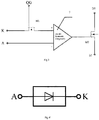
Fig. 3 is a functional block diagram of a reverse bias cut-off drive circuit. -
Fig. 4 is an equivalent circuit diagram of a rectifier diode replacement circuit. - In an Embodiment 1, referring to
Fig. 1 ,Fig. 3 and Fig. 4 , a rectifier diode replacement circuit having reverse bias cut-off drive includes a rectifier diode circuit and a reverse bias cut-off drive circuit 6; the rectifier diode circuit includes an energy storage capacitor C, a low-voltage clock generator 1, acharge pump circuit 2, a bandgap reference circuit 3, a hysteresis comparator 4, a drive amplifier 5 and a power MOS transistor Q;
the low-voltage clock generator 1 detects voltages at both ends A and K of the rectifier diode circuit and generates a clock signal to drive thecharge pump circuit 2;
thecharge pump circuit 2 detects voltages at both ends A and K of the rectifier diode circuit, and charges are stored into the energy storage capacitor C after being amplified;
voltages stored on the energy storage capacitor C and a reference voltage output by the bandgap reference circuit 3 are respectively output to the hysteresis comparator 4 so as to be compared; when the voltages stored on the energy storage capacitor 4 are greater than the reference voltage output by the bandgap reference circuit 3, the hysteresis comparator 4 outputs an on signal to be amplified by the drive amplifier 5 and then output to the power MOS transistor Q to drive the power MOS transistor Q to be on;
the reverse bias cut-off drive circuit 6 detects the voltages at both ends A and K of the rectifier diode circuit, and when a cathode potential is greater than an anode potential,
the reverse bias cut-off drive circuit 6 forms a rapid charge discharge channel at a gate of the power MOS transistor Q to cut off the power MOS transistor Q. - In the detailed embodiment, the reverse bias cut-off drive circuit 6 includes a transfer switch transistor M1, a
second hysteresis comparator 7 and a discharge switch transistor M2; the discharge switch transistor M2 is connected in parallel between the gate of the power MOS transistor Q and a negative end of the energy storage capacitor C and is controlled to be on or off by thesecond hysteresis comparator 7; the transfer switch transistor M1 is connected between the positive input end of thesecond hysteresis comparator 7 and the cathode of the rectifier diode circuit or between the negative input end of thesecond hysteresis comparator 7 and the anode of the rectifier diode circuit; the transfer switch transistor M1 is controlled to be on or off by the rectifier diode circuit; and thesecond hysteresis comparator 7 detects voltages at both ends A and K of the rectifier diode circuit, and when a cathode potential of the rectifier diode circuit is greater than an anode potential, thesecond hysteresis comparator 7 controls the discharge switch transistor M2 to be on to form a charge discharge channel at the gate of the power MOS transistor Q, so that the power MOS transistor Q is cut off. - Further, the transfer switch transistor M1 and the discharge switch transistor M2 are composed of MOSFETs; and a gate of the transfer switch transistor M1 is connected with an output of the drive amplifier 5, a source and drain of the discharge switch transistor M2 are connected in parallel between a gate of the power MOS transistor Q and a negative end of the energy storage capacitor C, and a gate of the discharge switch transistor M2 is connected with an output of the
second hysteresis comparator 7. - In an
Embodiment 2, referring toFig. 2 ,Fig. 3 and Fig. 4 , a rectifier diode replacement circuit having reverse bias cut-off drive includes a rectifier diode circuit and a reverse bias cut-off drive circuit 6; the rectifier diode circuit includes an energy storage capacitor C, a low-voltage clock generator 1, acharge pump circuit 2, a bandgap reference circuit 3, a hysteresis comparator 4, a drive amplifier 5 and a power MOS transistor Q;
the low-voltage clock generator 1 detects voltages at both ends A and K of the rectifier diode circuit and generates a clock signal to drive thecharge pump circuit 2;
thecharge pump circuit 2 detects voltages at both ends A and K of the rectifier diode circuit, and charges are stored into the energy storage capacitor C after being amplified;
voltages stored on the energy storage capacitor C and a reference voltage output by the bandgap reference circuit 3 are respectively output to the hysteresis comparator 4 so as to be compared; when the voltages stored on the energy storage capacitor 4 are greater than the reference voltage output by the bandgap reference circuit 3, the hysteresis comparator 4 outputs an on signal to be amplified by the drive amplifier 5 and then output to the power MOS transistor Q to drive the power MOS transistor Q to be on; and
the reverse bias cut-off drive circuit 6 detects voltages at both ends A and K of the rectifier diode circuit, when a cathode potential is greater than an anode potential, the reverse bias cut-off drive circuit 6 forms a charge discharge channel at both ends of the energy storage capacitor C so that the energy storage capacitor discharges by means of the reverse bias cut-off drive circuit, and the voltages at both ends of the energy storage capacitor C are rapidly dropped; and when the voltages at both ends of the energy storage capacitor C are lower than an output voltage of the bandgap reference circuit 3 in the rectifier diode circuit, the hysteresis comparator 4 outputs an off signal to cut off the power MOS transistor Q. - In the detailed embodiment, the reverse bias cut-off drive circuit 6 includes a transfer switch transistor M1, a
second hysteresis comparator 7 and a discharge switch transistor M2; the discharge switch transistor M2 is connected in parallel with the energy storage capacitor C and is controlled to be on or off by thesecond hysteresis comparator 7; the transfer switch transistor M1 is connected between the positive input end of thesecond hysteresis comparator 7 and the cathode of the rectifier diode circuit or between the negative input end of thesecond hysteresis comparator 7 and the anode of the rectifier diode circuit and is controlled to be on or off by the rectifier diode circuit; and thesecond hysteresis comparator 7 detects voltages at both ends of the rectifier diode circuit, when a cathode potential of the rectifier diode circuit is greater than an anode potential, thesecond hysteresis comparator 7 controls the discharge switch transistor M2 to be on so that the energy storage capacitor C discharges by means of the discharge switch transistor M2; and when the voltages at both ends of the energy storage capacitor C are lower than an output voltage of the bandgap reference circuit 3 in the rectifier diode circuit, the rectifier diode circuit outputs a control signal to cut off the power MOS transistor Q. - Further, the transfer switch transistor M1 and the discharge switch transistor M2 are composed of MOSFETs; and a gate of the transfer switch transistor M1 is connected with an output of the drive amplifier 5, a source and drain of the discharge switch transistor M2 are connected in parallel between both ends of the energy storage capacitor C, and a gate of the discharge switch transistor M2 is connected with an output of the
second hysteresis comparator 7. - In an embodiment 1 and an
embodiment 2, the average forward voltage is only about 150 mV. Therefore, the diode circuit has more obvious advantages than a special semiconductor device. However, if no reverse bias cut-off drive circuits are provided, the problem that rapid cut-off may not be realized during reverse bias may exist, the whole discharge period may be finished only when the voltage on the capacitor is dropped to be lower than a bandgap reference output voltage, and the rectifier diode circuit may enter a reverse bias cut-off state only if a power MOSFET is cut off. - If no reverse bias cut-off drive circuits are provided, the on resistance of the power MOSFET may be calculated to be 10 mΩ according to the the forward voltage drop 80 mV obtained in an on state of the power MOSFET when the current is 8A, and the input capacitance of the gate of the power MOSFET having the magnitude order of 10 mΩ is about several nF, in order to ignore influences of switch charge loss of the power MOSFET to the performance of the circuit, generally, the capacitance value of the energy storage capacitor C should be 100 nF or higher, therefore, both charge and discharge times of the diode circuit are longer, calculated according to an equation that T1/(T1+T2)=10% under the condition that the charge time T1 is equal to 5 ms and T2 is the discharge time, the discharge time is 45 ms, and the average on voltage is 152 mV, if being calculated according to an equation that T1/(T1+T2)=99%, the discharge time is 500 ms, the average on voltage is 87.2 mV, and therefore, it is more obvious to obtain a lower average on voltage if the discharge time is long, and after the diode circuit is converted from the forward bias to the reverse bias in the discharge state, the required cut-off time may be longer. An application of the diode circuit is to be seriously affected by such a problem.
- According to the technical solution of the present invention, the voltages at both ends of the diode circuit are actively detected in real time, and a rapid discharge channel is generated when the diode circuit is converted from the forward bias to the reverse bias, so that the discharge period is greatly shortened, and the diode circuit is rapidly cut off.
- In an Embodiment 3, a reverse bias cut-off drive circuit of a rectifier diode replacement circuit includes a transfer switch transistor M1, a
second hysteresis comparator 7 and a discharge switch transistor M2; the discharge switch transistor M2 is connected in parallel with the energy storage capacitor C in the rectifier diode replacement circuit and is controlled to be on or off by thesecond hysteresis comparator 7; the transfer switch transistor M1 is connected between the positive input end of thesecond hysteresis comparator 7 and the cathode of the rectifier diode replacement circuit, or the transfer switch transistor M1 is connected between the negative input end of thesecond hysteresis comparator 7 and the anode of the rectifier diode replacement circuit, thesecond hysteresis comparator 7 detects voltages at both ends of the rectifier diode replacement circuit, when a cathode potential of the rectifier diode replacement circuit is greater than an anode potential, thesecond hysteresis comparator 7 controls the discharge switch transistor M2 to be on so that the energy storage capacitor C discharges by means of the discharge switch transistor M2; and when the voltages at both ends of the energy storage capacitor C are lower than an output voltage of the bandgap reference circuit 3 in the rectifier diode replacement circuit, the rectifier diode replacement circuit outputs a control signal to cut off the power MOS transistor Q. - In the detailed embodiment, the transfer switch transistor M1 and the discharge switch transistor M2 are composed of MOSFETs; and a gate of the transfer switch transistor M1 is connected with an output of the drive amplifier 5, a source and drain of the discharge switch transistor M2 are connected in parallel between both ends of the energy storage capacitor C, and a gate of the discharge switch transistor M2 is connected with an output of the
second hysteresis comparator 7. In an Embodiment 4, a reverse bias cut-off drive circuit of a rectifier diode replacement circuit includes a transfer switch transistor M1, asecond hysteresis comparator 7 and a discharge switch transistor M2; the discharge switch transistor M2 is connected in parallel between the gate of the power MOS transistor Q and a negative end of the energy storage capacitor C in the rectifier diode replacement circuit and is controlled to be on or off by thesecond hysteresis comparator 7; the transfer switch transistor M1 is connected between the positive input end of thesecond hysteresis comparator 7 and the cathode of the rectifier diode replacement circuit, or the transfer switch transistor M1 is connected between the negative input end of thesecond hysteresis comparator 7 and the anode of the rectifier diode replacement circuit, thesecond hysteresis comparator 7 detects voltages at both ends of the rectifier diode replacement circuit, when a cathode potential of the rectifier diode replacement circuit is greater than an anode potential, thesecond hysteresis comparator 7 controls the discharge switch transistor M2 to be on to form a charge discharge channel at the gate of the power MOS transistor Q, so that the power MOS transistor Q is cut off; and when the voltages at both ends of the energy storage capacitor C are lower than an output voltage of the bandgap reference circuit 3 in the rectifier diode replacement circuit, the rectifier diode replacement circuit outputs a control signal to cut off the power MOS transistor Q. - In the detailed embodiment, the transfer switch transistor M1 and the discharge switch transistor M2 are composed of MOSFETs; and a gate of the transfer switch transistor M1 is connected with an output of the drive amplifier 5, a source and drain of the discharge switch transistor M2 are connected in parallel between a gate of the power MOS transistor Q and a negative end of the energy storage capacitor C, and a gate of the discharge switch transistor M2 is connected with an output of the
second hysteresis comparator 7. - The detailed embodiments of the present invention are described in detail above, however, the content protected by the present invention is not merely limited within the range of the detailed description.
Claims (6)
- A rectifier diode replacement circuit having an anode end and a cathode end, comprising a rectifier diode circuit and a reverse bias cut-off drive circuit; the rectifier diode circuit comprises an energy storage capacitor (C), a low-voltage clock generator (1), a charge pump circuit (2), a bandgap reference circuit (3), a hysteresis comparator (4), a drive amplifier (5) and a power MOS transistor (Q);
the low-voltage clock generator (1) is connected with both ends of the rectifier diode replacement circuit and adapted for detecting voltages at both ends of the rectifier diode replacement circuit and generating a clock signal to drive the charge pump circuit (2);
the charge pump circuit (2) is connected with the low-voltage clock generator (1), and the hysteresis comparator (4), and adapted for detecting voltages at both ends of the rectifier diode replacement circuit, and adapted for storing charges into the energy storage capacitor (C) after being amplified;
the rectifier diode circuit is adapted for outputting voltages stored on the energy storage capacitor (C) and a reference voltage output by the bandgap reference circuit (3), respectively, to the hysteresis comparator (4) so as to be compared;
the hysteresis comparator (4) is connected with the drive amplifier (5), and adapted for outputting an on signal to be amplified by the drive amplifier (5), when the voltages stored on the energy storage capacitor (4) are greater than the reference voltage output by the bandgap reference circuit (3);
the drive amplifier (5) is connected with the gate of the power MOS transistor (Q) and adapted for then outputing the amplified signal to the power MOS transistor (Q) to drive the power MOS transistor (Q) to be on wherein the source of the power MOS transistor (Q) is connected to the anode end of the rectifier diode replacement circuit and the drain of the power MOS transistor (Q) is connected to the cathode end of the rectifier diode replacement circuit;
characterized in that the reverse bias cut-off drive circuit (6) is connected with both ends of the rectifier diode replacement circuit, and adapted for detecting the voltages at both ends of the rectifier diode replacement circuit, and for forming a charge discharge channel at a gate of the power MOS transistor (Q) to cut off the power MOS transistor (Q), when a cathode potential is greater than an anode potential. - A rectifier diode replacement circuit having an anode end and a cathode end, comprising a rectifier diode circuit and a reverse bias cut-off drive circuit; the rectifier diode circuit comprises an energy storage capacitor (C), a low-voltage clock generator (1), a charge pump circuit (2), a bandgap reference circuit (3), a hysteresis comparator (4), a drive amplifier (5) and a power MOS transistor (Q);
the low-voltage clock generator (1) is connected with both ends of the rectifier diode replacement circuit and adapted for detecting voltages at both ends of the rectifier diode replacement circuit and generating a clock signal to drive the charge pump circuit (2);
the charge pump circuit (2) is connected with the low-voltage clock generator (1), and the hysteresis comparator (4), and adapted for detecting voltages at both ends of the rectifier diode replacement circuit, and adapted for storing charges into the energy storage capacitor (C) after being amplified;
the rectifier diode circuit is adapted for outputting voltages stored on the energy storage capacitor (C) and a reference voltage output by the bandgap reference circuit (3), respectively, to the hysteresis comparator (4) so as to be compared;
the hysteresis comparator (4) is connected with the drive amplifier (5), and adapted for outputting an on signal to be amplified by the drive amplifier (5), when the voltages stored on the energy storage capacitor (4) are greater than the reference voltage output by the bandgap reference circuit (3);
the drive amplifier (5) is connected with the gate of the power MOS transistor (Q) and adapted for then outputing the amplified signal to the power MOS transistor (Q) to drive the power MOS transistor (Q) to be on;
wherein the source of the power MOS transistor (Q) is connected to the anode end of the rectifier diode replacement circuit and the drain of the power MOS transistor (Q) is connected to the cathode end of the rectifier diode replacement circuit; wherein the reverse bias cut-off drive circuit (6) is connected with both ends of the rectifier diode replacement circuit and is adapted for forming a charge discharge channel at both ends of the energy storage capacitor (C) so that the energy storage capacitor (C) discharges by means of the reverse bias cut-off drive circuit (6) when a cathode potential is greater than an anode potential and the hysteresis comparator (4) is adapted for outputting an off signal to cut off the power MOS transistor (Q), when the voltages at both ends of the energy storage capacitor (C) are lower than an output voltage of the bandgap reference circuit (3) in the rectifier diode circuit. - The rectifier diode replacement circuit of claim 2, characterized in that the reverse bias cut-off drive circuit (6) comprises a transfer switch transistor (M1), a second hysteresis comparator (7) and a discharge switch transistor (M2); the discharge switch transistor (M2) is connected in parallel with the energy storage capacitor (C) and is controlled to be on or off by the second hysteresis comparator (7), and the transfer switch transistor (M1) is connected between the positive input end of the second hysteresis comparator (7) and the cathode (K) of the rectifier diode replacement circuit or between the negative input end of the second hysteresis comparator (7) and the anode (A) of the rectifier diode replacement circuit; the transfer switch transistor (M1) is adapted to be controlled to be on or off by the rectifier diode circuit; and the second hysteresis comparator (7) is connected with both ends of the rectifier diode replacement circuit, and adapted for detecting voltages at both ends of the rectifier diode replacement circuit; wherein, when a cathode potential of the rectifier diode replacement circuit is greater than an anode potential, the second hysteresis comparator (7) is adapted for controlling the discharge switch transistor (M2) to be on so that the energy storage capacitor (C) discharges by means of the discharge switch transistor; and when the voltages at both ends of the energy storage capacitor (C) are lower than an output voltage of the bandgap reference circuit (3) in the rectifier diode circuit, the rectifier diode circuit is adapted for outputting a control signal to cut off the power MOS transistor (Q).
- The rectifier diode replacement circuit of claim 1, characterized in that the reverse bias cut-off drive circuit comprises a transfer switch transistor (M1), a second hysteresis comparator (7) and a discharge switch transistor (M2); the discharge switch transistor (M2) is connected in parallel between a gate of the power MOS transistor (Q) and a negative end of the energy storage capacitor (C) and is controlled to be on or off by the second hysteresis comparator (7), and the transfer switch transistor (M1) is connected between the positive input end of the second hysteresis comparator (7) and the cathode (K) of the rectifier diode replacement circuit or between the negative input end of the second hysteresis comparator (7) and the anode (A) of the rectifier diode replacement circuit; the transfer switch transistor (M1) is adapted to be controlled to be on or off by the rectifier diode circuit; the second hysteresis comparator (7) is adapted for detecting voltages at both ends of the rectifier diode circuit, and when a cathode potential of the rectifier diode replacement circuit is greater than an anode potential, the second hysteresis comparator (7) controls the discharge switch transistor (M2) to be on to form a charge discharge channel at the gate (QG) of the power MOS transistor (Q), so that the power MOS transistor (Q) is cut off.
- The rectifier diode replacement circuit of claim 3, characterized in that the transfer switch transistor (M1) and the discharge switch transistor (M2) are composed of MOSFETs; and a gate of the transfer switch transistor (M1) is connected with an output of the drive amplifier (5), a source and drain of the discharge switch transistor (M2) are connected in parallel to both ends of the energy storage capacitor (C), and a gate of the discharge switch transistor (M2) is connected with an output of the second hysteresis comparator (7).
- The rectifier diode replacement circuit of claim 4, characterized in that the transfer switch transistor (M1) and the discharge switch transistor (M2) are composed of MOSFETs; and a gate of the transfer switch transistor (M1) is connected with an output of the drive amplifier (5), a source and drain of the discharge switch transistor (M2) are connected in parallel between a gate (QG) of the power MOS transistor (Q) and a negative end of the energy storage capacitor (C), and a gate of the discharge switch transistor (M2) is connected with an output of the second hysteresis comparator (7).
Applications Claiming Priority (2)
| Application Number | Priority Date | Filing Date | Title |
|---|---|---|---|
| CN201610734419.9A CN106253641B (en) | 2016-08-26 | 2016-08-26 | A kind of rectifier diode replacement circuit and reverse-biased cut-off driving circuit |
| PCT/CN2016/111191 WO2018036041A1 (en) | 2016-08-26 | 2016-12-21 | Rectifier diode replacement circuit and reverse bias cut-off drive circuit |
Publications (3)
| Publication Number | Publication Date |
|---|---|
| EP3416277A1 EP3416277A1 (en) | 2018-12-19 |
| EP3416277A4 EP3416277A4 (en) | 2019-10-09 |
| EP3416277B1 true EP3416277B1 (en) | 2020-09-23 |
Family
ID=57597616
Family Applications (1)
| Application Number | Title | Priority Date | Filing Date |
|---|---|---|---|
| EP16914061.3A Active EP3416277B1 (en) | 2016-08-26 | 2016-12-21 | Rectifier diode replacement circuit and reverse bias cut-off drive circuit |
Country Status (3)
| Country | Link |
|---|---|
| EP (1) | EP3416277B1 (en) |
| CN (1) | CN106253641B (en) |
| WO (1) | WO2018036041A1 (en) |
Families Citing this family (8)
| Publication number | Priority date | Publication date | Assignee | Title |
|---|---|---|---|---|
| CN109450416A (en) * | 2018-10-19 | 2019-03-08 | 福建和盛高科技产业有限公司 | A kind of high-current low-voltage difference diode equivalent circuit based on metal-oxide-semiconductor |
| DE102019104691B4 (en) * | 2019-02-25 | 2022-10-13 | Infineon Technologies Ag | diode circuit |
| CN110011523B (en) * | 2019-04-28 | 2023-12-29 | 苏州蓝博控制技术有限公司 | Power driving phase inverter and low-end driving to high-end driving circuit |
| CN111082502A (en) * | 2019-12-31 | 2020-04-28 | 深圳职业技术学院 | A kind of anti-backflow current MOS tube drive power generation circuit |
| CN116846233A (en) * | 2023-06-27 | 2023-10-03 | 桂林电子科技大学 | A high-efficiency CMOS rectifier circuit with threshold compensation |
| CN117595849A (en) * | 2023-10-20 | 2024-02-23 | 苏州华太电子技术股份有限公司 | ideal diode circuit |
| CN117595848A (en) * | 2023-10-20 | 2024-02-23 | 苏州华太电子技术股份有限公司 | Ideal diode circuit |
| CN117595850A (en) * | 2023-10-20 | 2024-02-23 | 苏州华太电子技术股份有限公司 | An ideal diode circuit |
Family Cites Families (14)
| Publication number | Priority date | Publication date | Assignee | Title |
|---|---|---|---|---|
| DE1192729B (en) * | 1961-06-12 | 1965-05-13 | Philips Nv | AC voltage regulator with premagnetized choke coil |
| US3697778A (en) * | 1971-03-17 | 1972-10-10 | Tektronix Inc | Integrating circuit |
| JPH08317656A (en) * | 1995-05-19 | 1996-11-29 | Nippondenso Co Ltd | Rectifying circuit |
| JP4442226B2 (en) * | 2004-01-05 | 2010-03-31 | 富士電機システムズ株式会社 | Synchronous rectifier circuit and power converter |
| CN200976577Y (en) * | 2006-11-29 | 2007-11-14 | 青岛海信电器股份有限公司 | MOS tube driving circuit and television set having the same |
| ITTO20110280A1 (en) * | 2011-03-29 | 2012-09-30 | Et99 S R L | SWITCHING CELLS TO POWER MOSFET TRANSISTORS |
| CN102904421B (en) * | 2012-09-24 | 2015-01-28 | 重庆西南集成电路设计有限责任公司 | High-performance rectifier diode replaced circuit |
| CN103647544B (en) * | 2013-11-27 | 2017-07-04 | 无锡中感微电子股份有限公司 | A kind of two-way transmission interface conversion circuit |
| CN203859683U (en) * | 2014-05-16 | 2014-10-01 | 西安唯电电气技术有限公司 | Synchronous rectification drive circuit |
| WO2016035120A1 (en) * | 2014-09-01 | 2016-03-10 | 三菱電機株式会社 | Dc-dc converter |
| CN104467422B (en) * | 2014-12-22 | 2017-04-26 | 英飞特电子(杭州)股份有限公司 | Constant-current Buck converter and constant-current control circuit thereof |
| DE102015001705B3 (en) * | 2015-02-13 | 2016-06-23 | Dialog Semiconductor (Uk) Limited | Current controlled active diode |
| CN104953859B (en) * | 2015-07-06 | 2019-03-22 | 安徽省东科半导体有限公司 | A kind of synchronous diode |
| CN205430205U (en) * | 2016-01-21 | 2016-08-03 | 唐柯 | Optical coupling isolation field pipe drive circuit |
-
2016
- 2016-08-26 CN CN201610734419.9A patent/CN106253641B/en active Active
- 2016-12-21 EP EP16914061.3A patent/EP3416277B1/en active Active
- 2016-12-21 WO PCT/CN2016/111191 patent/WO2018036041A1/en not_active Ceased
Non-Patent Citations (1)
| Title |
|---|
| None * |
Also Published As
| Publication number | Publication date |
|---|---|
| WO2018036041A1 (en) | 2018-03-01 |
| EP3416277A4 (en) | 2019-10-09 |
| CN106253641A (en) | 2016-12-21 |
| CN106253641B (en) | 2018-12-28 |
| EP3416277A1 (en) | 2018-12-19 |
Similar Documents
| Publication | Publication Date | Title |
|---|---|---|
| EP3416277A1 (en) | Rectifier diode replacement circuit and reverse bias cut-off drive circuit | |
| US11165423B2 (en) | Power switch drive circuit and device | |
| CN104426342B (en) | The charging of capacitor | |
| US6563725B2 (en) | Apparatus and method for control and driving BJT used as synchronous rectifier | |
| US9660551B2 (en) | Operating point optimization with double-base-contact bidirectional bipolar junction transistor circuits, methods, and systems | |
| CN209182668U (en) | Control Circuits and Control Systems | |
| US10587111B2 (en) | Short-circuit fault detection device | |
| JP2008546183A (en) | Protection circuit device for solar cell module | |
| US10587145B2 (en) | Charging circuit and electronic device | |
| US11632055B2 (en) | ACF converter, voltage conversion method, and electronic device | |
| US10651665B2 (en) | Current sense apparatus for battery charger systems | |
| CN108964465B (en) | Power converter with self-powered control mechanism | |
| CN102904421A (en) | High-performance rectifier diode replaced circuit | |
| US8958193B2 (en) | System and method for providing optically triggered circuit breaker | |
| US20180166971A1 (en) | Rectifier device | |
| WO2022236799A1 (en) | Voltage regulator module and integrated chip | |
| JP4101212B2 (en) | Power circuit | |
| KR20240142307A (en) | Device and method for driving gallium nitride device | |
| US9812966B2 (en) | Chopper circuit | |
| KR20140044466A (en) | Electrostatic discharge protection circuit | |
| JP3948530B2 (en) | Charging circuit and clock circuit | |
| US20160308525A1 (en) | Control system and control method for controlling a switching device integrated in an electronic converter and switching cell comprising said system | |
| CN111800012A (en) | Operating point control circuit arrangement for a plurality of power supply units connected in series | |
| Chen et al. | Enhance Gate Reliability and Threshold Voltage Stability of p-GaN Gate High-Electron-Mobility Transistors | |
| CN119210126A (en) | A power-off holding circuit and a power input protection circuit |
Legal Events
| Date | Code | Title | Description |
|---|---|---|---|
| STAA | Information on the status of an ep patent application or granted ep patent |
Free format text: STATUS: THE INTERNATIONAL PUBLICATION HAS BEEN MADE |
|
| PUAI | Public reference made under article 153(3) epc to a published international application that has entered the european phase |
Free format text: ORIGINAL CODE: 0009012 |
|
| STAA | Information on the status of an ep patent application or granted ep patent |
Free format text: STATUS: REQUEST FOR EXAMINATION WAS MADE |
|
| 17P | Request for examination filed |
Effective date: 20180914 |
|
| AK | Designated contracting states |
Kind code of ref document: A1 Designated state(s): AL AT BE BG CH CY CZ DE DK EE ES FI FR GB GR HR HU IE IS IT LI LT LU LV MC MK MT NL NO PL PT RO RS SE SI SK SM TR |
|
| AX | Request for extension of the european patent |
Extension state: BA ME |
|
| RIC1 | Information provided on ipc code assigned before grant |
Ipc: H02M 1/08 20060101ALI20190829BHEP Ipc: H03K 17/042 20060101ALI20190829BHEP Ipc: H02M 7/217 20060101AFI20190829BHEP Ipc: H03K 17/30 20060101ALI20190829BHEP Ipc: H03K 17/04 20060101ALI20190829BHEP |
|
| A4 | Supplementary search report drawn up and despatched |
Effective date: 20190906 |
|
| DAV | Request for validation of the european patent (deleted) | ||
| DAX | Request for extension of the european patent (deleted) | ||
| GRAP | Despatch of communication of intention to grant a patent |
Free format text: ORIGINAL CODE: EPIDOSNIGR1 |
|
| STAA | Information on the status of an ep patent application or granted ep patent |
Free format text: STATUS: GRANT OF PATENT IS INTENDED |
|
| INTG | Intention to grant announced |
Effective date: 20200616 |
|
| GRAS | Grant fee paid |
Free format text: ORIGINAL CODE: EPIDOSNIGR3 |
|
| GRAA | (expected) grant |
Free format text: ORIGINAL CODE: 0009210 |
|
| STAA | Information on the status of an ep patent application or granted ep patent |
Free format text: STATUS: THE PATENT HAS BEEN GRANTED |
|
| AK | Designated contracting states |
Kind code of ref document: B1 Designated state(s): AL AT BE BG CH CY CZ DE DK EE ES FI FR GB GR HR HU IE IS IT LI LT LU LV MC MK MT NL NO PL PT RO RS SE SI SK SM TR |
|
| REG | Reference to a national code |
Ref country code: GB Ref legal event code: FG4D |
|
| REG | Reference to a national code |
Ref country code: CH Ref legal event code: EP |
|
| REG | Reference to a national code |
Ref country code: IE Ref legal event code: FG4D |
|
| REG | Reference to a national code |
Ref country code: AT Ref legal event code: REF Ref document number: 1317393 Country of ref document: AT Kind code of ref document: T Effective date: 20201015 Ref country code: DE Ref legal event code: R096 Ref document number: 602016044789 Country of ref document: DE |
|
| REG | Reference to a national code |
Ref country code: NL Ref legal event code: FP |
|
| PG25 | Lapsed in a contracting state [announced via postgrant information from national office to epo] |
Ref country code: HR Free format text: LAPSE BECAUSE OF FAILURE TO SUBMIT A TRANSLATION OF THE DESCRIPTION OR TO PAY THE FEE WITHIN THE PRESCRIBED TIME-LIMIT Effective date: 20200923 Ref country code: FI Free format text: LAPSE BECAUSE OF FAILURE TO SUBMIT A TRANSLATION OF THE DESCRIPTION OR TO PAY THE FEE WITHIN THE PRESCRIBED TIME-LIMIT Effective date: 20200923 Ref country code: BG Free format text: LAPSE BECAUSE OF FAILURE TO SUBMIT A TRANSLATION OF THE DESCRIPTION OR TO PAY THE FEE WITHIN THE PRESCRIBED TIME-LIMIT Effective date: 20201223 Ref country code: SE Free format text: LAPSE BECAUSE OF FAILURE TO SUBMIT A TRANSLATION OF THE DESCRIPTION OR TO PAY THE FEE WITHIN THE PRESCRIBED TIME-LIMIT Effective date: 20200923 Ref country code: GR Free format text: LAPSE BECAUSE OF FAILURE TO SUBMIT A TRANSLATION OF THE DESCRIPTION OR TO PAY THE FEE WITHIN THE PRESCRIBED TIME-LIMIT Effective date: 20201224 Ref country code: NO Free format text: LAPSE BECAUSE OF FAILURE TO SUBMIT A TRANSLATION OF THE DESCRIPTION OR TO PAY THE FEE WITHIN THE PRESCRIBED TIME-LIMIT Effective date: 20201223 |
|
| PG25 | Lapsed in a contracting state [announced via postgrant information from national office to epo] |
Ref country code: RS Free format text: LAPSE BECAUSE OF FAILURE TO SUBMIT A TRANSLATION OF THE DESCRIPTION OR TO PAY THE FEE WITHIN THE PRESCRIBED TIME-LIMIT Effective date: 20200923 Ref country code: LV Free format text: LAPSE BECAUSE OF FAILURE TO SUBMIT A TRANSLATION OF THE DESCRIPTION OR TO PAY THE FEE WITHIN THE PRESCRIBED TIME-LIMIT Effective date: 20200923 |
|
| REG | Reference to a national code |
Ref country code: LT Ref legal event code: MG4D |
|
| PG25 | Lapsed in a contracting state [announced via postgrant information from national office to epo] |
Ref country code: SM Free format text: LAPSE BECAUSE OF FAILURE TO SUBMIT A TRANSLATION OF THE DESCRIPTION OR TO PAY THE FEE WITHIN THE PRESCRIBED TIME-LIMIT Effective date: 20200923 Ref country code: EE Free format text: LAPSE BECAUSE OF FAILURE TO SUBMIT A TRANSLATION OF THE DESCRIPTION OR TO PAY THE FEE WITHIN THE PRESCRIBED TIME-LIMIT Effective date: 20200923 Ref country code: CZ Free format text: LAPSE BECAUSE OF FAILURE TO SUBMIT A TRANSLATION OF THE DESCRIPTION OR TO PAY THE FEE WITHIN THE PRESCRIBED TIME-LIMIT Effective date: 20200923 Ref country code: RO Free format text: LAPSE BECAUSE OF FAILURE TO SUBMIT A TRANSLATION OF THE DESCRIPTION OR TO PAY THE FEE WITHIN THE PRESCRIBED TIME-LIMIT Effective date: 20200923 Ref country code: PT Free format text: LAPSE BECAUSE OF FAILURE TO SUBMIT A TRANSLATION OF THE DESCRIPTION OR TO PAY THE FEE WITHIN THE PRESCRIBED TIME-LIMIT Effective date: 20210125 Ref country code: LT Free format text: LAPSE BECAUSE OF FAILURE TO SUBMIT A TRANSLATION OF THE DESCRIPTION OR TO PAY THE FEE WITHIN THE PRESCRIBED TIME-LIMIT Effective date: 20200923 |
|
| PG25 | Lapsed in a contracting state [announced via postgrant information from national office to epo] |
Ref country code: AL Free format text: LAPSE BECAUSE OF FAILURE TO SUBMIT A TRANSLATION OF THE DESCRIPTION OR TO PAY THE FEE WITHIN THE PRESCRIBED TIME-LIMIT Effective date: 20200923 Ref country code: ES Free format text: LAPSE BECAUSE OF FAILURE TO SUBMIT A TRANSLATION OF THE DESCRIPTION OR TO PAY THE FEE WITHIN THE PRESCRIBED TIME-LIMIT Effective date: 20200923 Ref country code: PL Free format text: LAPSE BECAUSE OF FAILURE TO SUBMIT A TRANSLATION OF THE DESCRIPTION OR TO PAY THE FEE WITHIN THE PRESCRIBED TIME-LIMIT Effective date: 20200923 Ref country code: IS Free format text: LAPSE BECAUSE OF FAILURE TO SUBMIT A TRANSLATION OF THE DESCRIPTION OR TO PAY THE FEE WITHIN THE PRESCRIBED TIME-LIMIT Effective date: 20210123 |
|
| REG | Reference to a national code |
Ref country code: DE Ref legal event code: R097 Ref document number: 602016044789 Country of ref document: DE |
|
| PG25 | Lapsed in a contracting state [announced via postgrant information from national office to epo] |
Ref country code: SK Free format text: LAPSE BECAUSE OF FAILURE TO SUBMIT A TRANSLATION OF THE DESCRIPTION OR TO PAY THE FEE WITHIN THE PRESCRIBED TIME-LIMIT Effective date: 20200923 |
|
| PLBE | No opposition filed within time limit |
Free format text: ORIGINAL CODE: 0009261 |
|
| REG | Reference to a national code |
Ref country code: CH Ref legal event code: PL |
|
| STAA | Information on the status of an ep patent application or granted ep patent |
Free format text: STATUS: NO OPPOSITION FILED WITHIN TIME LIMIT |
|
| PG25 | Lapsed in a contracting state [announced via postgrant information from national office to epo] |
Ref country code: SI Free format text: LAPSE BECAUSE OF FAILURE TO SUBMIT A TRANSLATION OF THE DESCRIPTION OR TO PAY THE FEE WITHIN THE PRESCRIBED TIME-LIMIT Effective date: 20200923 Ref country code: DK Free format text: LAPSE BECAUSE OF FAILURE TO SUBMIT A TRANSLATION OF THE DESCRIPTION OR TO PAY THE FEE WITHIN THE PRESCRIBED TIME-LIMIT Effective date: 20200923 Ref country code: MC Free format text: LAPSE BECAUSE OF FAILURE TO SUBMIT A TRANSLATION OF THE DESCRIPTION OR TO PAY THE FEE WITHIN THE PRESCRIBED TIME-LIMIT Effective date: 20200923 |
|
| 26N | No opposition filed |
Effective date: 20210624 |
|
| REG | Reference to a national code |
Ref country code: BE Ref legal event code: MM Effective date: 20201231 |
|
| PG25 | Lapsed in a contracting state [announced via postgrant information from national office to epo] |
Ref country code: IE Free format text: LAPSE BECAUSE OF NON-PAYMENT OF DUE FEES Effective date: 20201221 Ref country code: LU Free format text: LAPSE BECAUSE OF NON-PAYMENT OF DUE FEES Effective date: 20201221 Ref country code: IT Free format text: LAPSE BECAUSE OF FAILURE TO SUBMIT A TRANSLATION OF THE DESCRIPTION OR TO PAY THE FEE WITHIN THE PRESCRIBED TIME-LIMIT Effective date: 20200923 |
|
| PG25 | Lapsed in a contracting state [announced via postgrant information from national office to epo] |
Ref country code: CH Free format text: LAPSE BECAUSE OF NON-PAYMENT OF DUE FEES Effective date: 20201231 Ref country code: LI Free format text: LAPSE BECAUSE OF NON-PAYMENT OF DUE FEES Effective date: 20201231 |
|
| PG25 | Lapsed in a contracting state [announced via postgrant information from national office to epo] |
Ref country code: TR Free format text: LAPSE BECAUSE OF FAILURE TO SUBMIT A TRANSLATION OF THE DESCRIPTION OR TO PAY THE FEE WITHIN THE PRESCRIBED TIME-LIMIT Effective date: 20200923 Ref country code: MT Free format text: LAPSE BECAUSE OF FAILURE TO SUBMIT A TRANSLATION OF THE DESCRIPTION OR TO PAY THE FEE WITHIN THE PRESCRIBED TIME-LIMIT Effective date: 20200923 Ref country code: CY Free format text: LAPSE BECAUSE OF FAILURE TO SUBMIT A TRANSLATION OF THE DESCRIPTION OR TO PAY THE FEE WITHIN THE PRESCRIBED TIME-LIMIT Effective date: 20200923 |
|
| PG25 | Lapsed in a contracting state [announced via postgrant information from national office to epo] |
Ref country code: MK Free format text: LAPSE BECAUSE OF FAILURE TO SUBMIT A TRANSLATION OF THE DESCRIPTION OR TO PAY THE FEE WITHIN THE PRESCRIBED TIME-LIMIT Effective date: 20200923 |
|
| PG25 | Lapsed in a contracting state [announced via postgrant information from national office to epo] |
Ref country code: BE Free format text: LAPSE BECAUSE OF NON-PAYMENT OF DUE FEES Effective date: 20201231 |
|
| REG | Reference to a national code |
Ref country code: AT Ref legal event code: UEP Ref document number: 1317393 Country of ref document: AT Kind code of ref document: T Effective date: 20200923 |
|
| PGFP | Annual fee paid to national office [announced via postgrant information from national office to epo] |
Ref country code: NL Payment date: 20251117 Year of fee payment: 10 |
|
| PGFP | Annual fee paid to national office [announced via postgrant information from national office to epo] |
Ref country code: GB Payment date: 20251111 Year of fee payment: 10 |
|
| PGFP | Annual fee paid to national office [announced via postgrant information from national office to epo] |
Ref country code: AT Payment date: 20251215 Year of fee payment: 10 |
|
| PGFP | Annual fee paid to national office [announced via postgrant information from national office to epo] |
Ref country code: FR Payment date: 20251110 Year of fee payment: 10 |
|
| PGFP | Annual fee paid to national office [announced via postgrant information from national office to epo] |
Ref country code: DE Payment date: 20251222 Year of fee payment: 10 |