EP3416174A1 - Articulated direct-mount inductor and associated systems and methods - Google Patents
Articulated direct-mount inductor and associated systems and methods Download PDFInfo
- Publication number
- EP3416174A1 EP3416174A1 EP18175467.2A EP18175467A EP3416174A1 EP 3416174 A1 EP3416174 A1 EP 3416174A1 EP 18175467 A EP18175467 A EP 18175467A EP 3416174 A1 EP3416174 A1 EP 3416174A1
- Authority
- EP
- European Patent Office
- Prior art keywords
- mount inductor
- coil portion
- mounting structure
- articulated direct
- inductor
- Prior art date
- Legal status (The legal status is an assumption and is not a legal conclusion. Google has not performed a legal analysis and makes no representation as to the accuracy of the status listed.)
- Granted
Links
Images





Classifications
-
- H—ELECTRICITY
- H01—ELECTRIC ELEMENTS
- H01F—MAGNETS; INDUCTANCES; TRANSFORMERS; SELECTION OF MATERIALS FOR THEIR MAGNETIC PROPERTIES
- H01F27/00—Details of transformers or inductances, in general
- H01F27/28—Coils; Windings; Conductive connections
-
- H—ELECTRICITY
- H01—ELECTRIC ELEMENTS
- H01F—MAGNETS; INDUCTANCES; TRANSFORMERS; SELECTION OF MATERIALS FOR THEIR MAGNETIC PROPERTIES
- H01F27/00—Details of transformers or inductances, in general
- H01F27/28—Coils; Windings; Conductive connections
- H01F27/30—Fastening or clamping coils, windings, or parts thereof together; Fastening or mounting coils or windings on core, casing, or other support
- H01F27/306—Fastening or mounting coils or windings on core, casing or other support
-
- H—ELECTRICITY
- H01—ELECTRIC ELEMENTS
- H01F—MAGNETS; INDUCTANCES; TRANSFORMERS; SELECTION OF MATERIALS FOR THEIR MAGNETIC PROPERTIES
- H01F27/00—Details of transformers or inductances, in general
- H01F27/08—Cooling; Ventilating
-
- H—ELECTRICITY
- H01—ELECTRIC ELEMENTS
- H01F—MAGNETS; INDUCTANCES; TRANSFORMERS; SELECTION OF MATERIALS FOR THEIR MAGNETIC PROPERTIES
- H01F27/00—Details of transformers or inductances, in general
- H01F27/24—Magnetic cores
-
- H—ELECTRICITY
- H01—ELECTRIC ELEMENTS
- H01F—MAGNETS; INDUCTANCES; TRANSFORMERS; SELECTION OF MATERIALS FOR THEIR MAGNETIC PROPERTIES
- H01F27/00—Details of transformers or inductances, in general
- H01F27/28—Coils; Windings; Conductive connections
- H01F27/2847—Sheets; Strips
-
- H—ELECTRICITY
- H01—ELECTRIC ELEMENTS
- H01F—MAGNETS; INDUCTANCES; TRANSFORMERS; SELECTION OF MATERIALS FOR THEIR MAGNETIC PROPERTIES
- H01F27/00—Details of transformers or inductances, in general
- H01F27/28—Coils; Windings; Conductive connections
- H01F27/2847—Sheets; Strips
- H01F27/2852—Construction of conductive connections, of leads
-
- H—ELECTRICITY
- H01—ELECTRIC ELEMENTS
- H01F—MAGNETS; INDUCTANCES; TRANSFORMERS; SELECTION OF MATERIALS FOR THEIR MAGNETIC PROPERTIES
- H01F27/00—Details of transformers or inductances, in general
- H01F27/28—Coils; Windings; Conductive connections
- H01F27/29—Terminals; Tapping arrangements for signal inductances
- H01F27/292—Surface mounted devices
-
- H—ELECTRICITY
- H01—ELECTRIC ELEMENTS
- H01F—MAGNETS; INDUCTANCES; TRANSFORMERS; SELECTION OF MATERIALS FOR THEIR MAGNETIC PROPERTIES
- H01F27/00—Details of transformers or inductances, in general
- H01F27/34—Special means for preventing or reducing unwanted electric or magnetic effects, e.g. no-load losses, reactive currents, harmonics, oscillations, leakage fields
- H01F27/346—Preventing or reducing leakage fields
-
- H—ELECTRICITY
- H01—ELECTRIC ELEMENTS
- H01F—MAGNETS; INDUCTANCES; TRANSFORMERS; SELECTION OF MATERIALS FOR THEIR MAGNETIC PROPERTIES
- H01F27/00—Details of transformers or inductances, in general
- H01F27/40—Structural association with built-in electric component, e.g. fuse
-
- H—ELECTRICITY
- H01—ELECTRIC ELEMENTS
- H01F—MAGNETS; INDUCTANCES; TRANSFORMERS; SELECTION OF MATERIALS FOR THEIR MAGNETIC PROPERTIES
- H01F41/00—Apparatus or processes specially adapted for manufacturing or assembling magnets, inductances or transformers; Apparatus or processes specially adapted for manufacturing materials characterised by their magnetic properties
-
- H—ELECTRICITY
- H01—ELECTRIC ELEMENTS
- H01F—MAGNETS; INDUCTANCES; TRANSFORMERS; SELECTION OF MATERIALS FOR THEIR MAGNETIC PROPERTIES
- H01F41/00—Apparatus or processes specially adapted for manufacturing or assembling magnets, inductances or transformers; Apparatus or processes specially adapted for manufacturing materials characterised by their magnetic properties
- H01F41/02—Apparatus or processes specially adapted for manufacturing or assembling magnets, inductances or transformers; Apparatus or processes specially adapted for manufacturing materials characterised by their magnetic properties for manufacturing cores, coils, or magnets
- H01F41/04—Apparatus or processes specially adapted for manufacturing or assembling magnets, inductances or transformers; Apparatus or processes specially adapted for manufacturing materials characterised by their magnetic properties for manufacturing cores, coils, or magnets for manufacturing coils
- H01F41/06—Coil winding
-
- H—ELECTRICITY
- H01—ELECTRIC ELEMENTS
- H01F—MAGNETS; INDUCTANCES; TRANSFORMERS; SELECTION OF MATERIALS FOR THEIR MAGNETIC PROPERTIES
- H01F5/00—Coils
- H01F5/04—Arrangements of electric connections to coils, e.g. leads
-
- H—ELECTRICITY
- H01—ELECTRIC ELEMENTS
- H01J—ELECTRIC DISCHARGE TUBES OR DISCHARGE LAMPS
- H01J37/00—Discharge tubes with provision for introducing objects or material to be exposed to the discharge, e.g. for the purpose of examination or processing thereof
- H01J37/32—Gas-filled discharge tubes
- H01J37/32009—Arrangements for generation of plasma specially adapted for examination or treatment of objects, e.g. plasma sources
- H01J37/32082—Radio frequency generated discharge
- H01J37/32174—Circuits specially adapted for controlling the RF discharge
- H01J37/32183—Matching circuits
-
- H—ELECTRICITY
- H03—ELECTRONIC CIRCUITRY
- H03H—IMPEDANCE NETWORKS, e.g. RESONANT CIRCUITS; RESONATORS
- H03H3/00—Apparatus or processes specially adapted for the manufacture of impedance networks, resonating circuits, resonators
-
- H—ELECTRICITY
- H03—ELECTRONIC CIRCUITRY
- H03H—IMPEDANCE NETWORKS, e.g. RESONANT CIRCUITS; RESONATORS
- H03H7/00—Multiple-port networks comprising only passive electrical elements as network components
- H03H7/38—Impedance-matching networks
Definitions
- the present invention relates to semiconductor device fabrication.
- radiofrequency power is transmitted to a processing chamber to generate plasma and/or generate bias voltage and/or produce some other desired effect.
- the radiofrequency power is generated by a radiofrequency power supply and is transmitted through an impedance matching system in route to the processing chamber.
- the impedance matching system is configured to ensure that a load impedance seen by the radiofrequency power supply is sufficient close to a load impedance for which the radiofrequency power supply is designed, so that radiofrequency power will be efficiently transmitted to the load within the processing chamber without unacceptable radiofrequency signal reflection and/or loss. Transmission of the radiofrequency power through the impedance matching system can cause heating of components within the impedance matching system that must be managed to avoid thermally-induced damage. It is within this context that the present invention arises.
- an articulated direct-mount inductor in an example embodiment, includes a coil portion of an electrically conductive material.
- the articulated direct-mount inductor also includes a first articulation portion of the electrically conductive material extending from the coil portion.
- the articulated direct-mount inductor also includes a first mounting structure of the electrically conductive material extending from the first articulation portion.
- the first mounting structure includes a first mounting region configured to mount in physical and electrical contact with a terminal of a first electrical component.
- the first articulation portion and the first mounting structure are collectively configured to position the first mounting region at a location outside of a strong electromagnetic field emanating from the coil portion when radiofrequency power is transmitted through the articulated direct-mount inductor.
- the articulated direct-mount inductor also includes a second articulation portion of the electrically conductive material extending from the coil portion.
- the articulated direct-mount inductor also includes a second mounting structure of the electrically conductive material extending from the second articulation portion.
- the second mounting structure includes a second mounting region configured to mount in physical and electrical contact with a terminal of a second electrical component.
- the second articulation portion and the second mounting structure are collectively configured to position the second mounting region at a location outside of the strong electromagnetic field emanating from the coil portion when radiofrequency power is transmitted through the articulated direct-mount inductor.
- a method for configuring an impedance matching system.
- the method includes providing an articulated direct-mount inductor configured to directly connect to at least two electrical components at respective locations outside of a strong electromagnetic field emanating from a coil portion of the articulated direct-mount inductor when radiofrequency power is transmitted through the articulated direct-mount inductor.
- the articulated direct-mount inductor includes a first articulation portion extending from the coil portion to a first mounting portion.
- the articulated direct-mount inductor also includes a second articulation portion extending from the coil portion to a second mounting structure.
- the method also includes connecting the articulated direct-mount inductor directly to the at least two electrical components.
- a method for manufacturing an articulated direct-mount inductor.
- the method includes laying out an entirety of the articulated direct-mount inductor in a planar form on a planar sheet of electrically conductive material.
- the articulated direct-mount inductor in its planar form includes a rectangular-shaped region, and a first mounting structure region located at a first end of the rectangular-shaped region, and a second mounting structure region located at a second end of the rectangular-shaped region.
- the method also includes cutting out the entirety of the articulated direct-mount inductor in its planar form from the planar sheet of electrically conductive material.
- the method also includes wrapping a portion of the rectangular-shaped region of the articulated direct-mount inductor in its planar form around a core formation structure to form a helical-shaped coil portion.
- the method also includes removing the core formation structure from within the helical-shaped coil portion.
- the method also includes bending a portion of the articulated direct-mount inductor in its planar form between the helical-shaped coil portion and the first mounting structure region to form a first articulation portion.
- the method also includes bending a portion of the articulated direct-mount inductor in its planar form between the helical-shaped coil portion and the second mounting structure region to form a second articulation portion.
- the first articulation portion and the second articulation portion are formed to enable connection of the first mounting structure and the second mounting structure, respectively, to electrical components to which the articulated direct-mount inductor directly interfaces.
- FIG. 1A shows an example vertical cross-section diagram of a CCP processing chamber 101, in accordance with some embodiments of the present invention.
- the CCP processing chamber 101 defines a processing volume within which a plasma 123 is generated in exposure to a substrate 105 to affect a change to the substrate 105 in a controlled manner.
- the change to the substrate 105 can be a change in material or surface condition on the substrate 105.
- the change to the substrate 105 can include one or more of etching of a material from the substrate 105, deposition of a material on the substrate 105, or modification of material 105 present on the substrate 105.
- the substrate 105 is a semiconductor wafer undergoing a fabrication procedure.
- the substrate 105 can be essentially any type of substrate that is subjected to a plasma-based fabrication process.
- the term substrate 105 as used herein can refer to substrates formed of sapphire, GaN, GaAs or SiC, or other substrate materials, and can include glass panels/substrates, metal foils, metal sheets, polymer materials, or the like.
- the substrate 105 as referred to herein may vary in form, shape, and/or size.
- the substrate 105 referred to herein may correspond to a 200 mm (millimeters) semiconductor wafer, a 300 mm semiconductor wafer, or a 450 mm semiconductor wafer.
- the substrate 105 referred to herein may correspond to a non-circular substrate, such as a rectangular substrate for a flat panel display, or the like, among other shapes.
- the CCP processing chamber 101 operates by flowing one or more process gases into the processing volume, and by applying radiofrequency power to the one or more process gases to transform the one or more process gases into the plasma 123 in exposure to the substrate 105, in order to affect a change in material or surface condition on the substrate 105.
- the CCP processing chamber 101 includes a substrate support structure 103 upon which the substrate 105 is positioned and supported during processing operations.
- an electrode 107 is disposed within the substrate support structure 103 to provide for transmission of radiofrequency power from the electrode 107 through the processing volume to generate the plasma 123.
- the electrode 107 is connected to receive radiofrequency power through a radiofrequency power supply structure 109, which is connected to one or more radiofrequency signal generator(s) 111 by way of one or more impedance matching system(s) 113.
- the matching system(s) 113 include an arrangement of capacitors and inductors configured to ensure that an impedance seen by the radiofrequency signal generator(s) 111 at the radiofrequency power supply structure 109 is sufficiently close to a load impedance for which the radiofrequency signal generator(s) 111 is designed to operate, so that radiofrequency signals generated and transmitted by the radiofrequency signal generator(s) 111 will be transmitted into the processing volume in an efficient manner, i.e., without unacceptable reflection.
- an upper electrode 115 can also be provided.
- the upper electrode 115 can provide either an electrical ground electrode or can be used to transmit radiofrequency power into the processing volume.
- the upper electrode 115 is connected to receive radiofrequency power through a radiofrequency power supply structure 117, which is connected to one or more radiofrequency signal generator(s) 121 by way of one or more impedance matching system(s) 119.
- the matching system(s) 119 include an arrangement of capacitors and inductors configured to ensure that an impedance seen by the radiofrequency signal generator(s) 121 at the radiofrequency power supply structure 117 is sufficiently close to a load impedance for which the radiofrequency signal generator(s) 121 is designed to operate, so that radiofrequency signals generated and transmitted by the radiofrequency signal generator(s) 121 will be transmitted into the processing volume in an efficient manner, i.e., without unacceptable reflection.
- FIG. 1B shows an example vertical cross-section diagram of an ICP processing chamber 151, in accordance with some embodiments of the present invention.
- the ICP processing chamber can also be referred to as a transformer coupled plasma (TCP) processing chamber.
- TCP transformer coupled plasma
- ICP processing chamber will be used to refer to both ICP and TCP processing chambers.
- the ICP processing chamber 151 defines a processing volume within which the plasma 123 is generated in exposure to the substrate 105 to affect a change to the substrate 105 in a controlled manner.
- the change to the substrate 105 can be a change in material or surface condition on the substrate 105.
- the change to the substrate 105 can include one or more of etching of a material from the substrate 105, deposition of a material on the substrate 105, or modification of material 105 present on the substrate 105.
- the ICP processing chamber 150 can be any type of ICP processing chamber in which radiofrequency signals are transmitted from a coil 155 disposed outside the ICP processing chamber 151 to a process gas within the ICP processing chamber 151 to generate the plasma 123 within the ICP processing chamber 151.
- An upper window structure 153 is provided to allow for transmission of radiofrequency signals from the coil 155 through the upper window structure 153 and into the processing volume of the ICP processing chamber 151.
- the ICP processing chamber 150 operates by flowing one or more process gases into the processing volume, and by applying radiofrequency power from the coil 155 to the one or more process gases to transform the one or more process gases into the plasma 123 in exposure to the substrate 105, in order to affect a change in material or surface condition on the substrate 105.
- the coil 155 is disposed above the upper window structure 153.
- the coil 155 is formed as a radial coil assembly, with the shaded parts of the coil 155 turning into the page of the drawing and with the unshaded parts of the coil 155 turning out of the page of the drawing.
- the coil 155 can be of essentially any configuration that is suitable for transmitting radiofrequency power through the upper window structure 153 and into the plasma processing volume.
- the coil 155 can have any number of turns and any cross-section size and shape (circular, oval, rectangular, trapezoidal, etc.) as required to provide the necessary transmission of radiofrequency signals through the upper window structure 153 into the processing volume.
- the coil 155 is connected through a radiofrequency power supply structure 161 to one or more radiofrequency signal generator(s) 157 by way of one or more matching system(s) 159.
- the matching system(s) 159 includes an arrangement of capacitors and/or inductors configured to ensure that an impedance seen by the radiofrequency signal generator(s) 157 at the coil 155 is sufficiently close to a load impedance for which the radiofrequency signal generator(s) 157 is designed to operate, so that radiofrequency signals supplied to the coil 155 by the primary radiofrequency signal generator(s) 157 will be transmitted into the processing volume in an efficient manner, i.e., without unacceptable reflection.
- the ICP processing chamber 151 can include the electrode 107, the radiofrequency power supply structure 109, the matching system(s) 113, and the radiofrequency signal generator(s) 111, as previously described with regard to Figure 1A .
- FIG. 1C shows a configuration of an example impedance matching system 170, in accordance with some embodiments of the present invention.
- the example impedance matching system 170 can be used for any of the matching systems 119, 113, 159 shown in Figures 1A and 1B .
- the impedance matching system 170 includes an electronics region 171 that includes control boards, cables, and server motors for controlling settings of variable capacitors.
- the impedance matching system 170 also includes a variable capacitors/inductor region 173 that includes a number of variable capacitors positioned and connected to be controlled by the sever motors within the electronics region 171.
- the variable capacitors/inductor region 173 also includes at least one inductor connected to electrical components, such as to a number of the variable capacitors.
- variable capacitors/inductor region 173 can also include a number of voltage-current (VI) sensors and corresponding connection structures.
- the impedance matching system 170 includes a fixed capacitors/radiofrequency plugs region 175 that includes a number of fixed capacitors and a number of radiofrequency plugs 177 configured to provide for electrical connection to the chamber coil(s) and/or electrode(s).
- the various components disposed within the example impedance matching system 170 are connected to form an impedance matching circuit that functions to substantially match an impedance of the load, i.e., of the plasma 123, to an impedance of the radiofrequency signal source, i.e., to the impedance of the radiofrequency signal generator(s) 121, 111, 157, so that radiofrequency power will be efficiently transferred to the load.
- the configuration of the example impedance matching system 170 discussed above is provided to facilitate description of the present invention and is not intended to be limiting. In other embodiments, the invention disclosed herein can be used with essentially any impedance matching system configuration.
- Figure 1D shows an example configuration of the variable capacitors/inductor region 173, including a radiofrequency signal supply input terminal 182.
- the variable capacitors/inductor region 173 includes multiple VI sensors 189A, 189B.
- the incoming radiofrequency signal(s) are transmitted to a first terminal of a variable capacitor 184.
- a second terminal of the variable capacitor 184 is connected to a first terminal of a variable capacitor 187.
- a second terminal of the variable capacitor 187 is connected to a first end of a conventional inductor 181, through a connection strap 186.
- Figure 1E shows a closer view of the mechanical/electrical connection between the second terminal of the variable capacitor 187 and a first connection region 181A at the first end of the conventional inductor 181, through the connection strap 186.
- the first connection region 181A of the conventional inductor 181 includes a pair of holes to accommodate fasteners 191A for securing the conventional inductor 181 to the connection strap 186.
- Figure 1D also shows a second terminal of the conventional inductor 181 connected to both a first terminal of a variable capacitor 183 and a first terminal of a variable capacitor 185, through a connection strap 188.
- Figure 1F shows a closer view of the mechanical/electrical connection between a second connection region 181B of the conventional inductor 181 and each of the first terminal of the variable capacitor 183 and the first terminal of the variable capacitor 185, through the connection strap 188.
- the second connection region 181B of the conventional inductor 181 includes a pair of holes to accommodate fasteners 191B for securing the conventional inductor 181 to the connection strap 188.
- variable capacitors/inductor region 173 can include more or less components than those discussed above.
- Figure 1G shows an isometric view of the conventional inductor 181.
- the conventional inductor 181 is formed as a simple coil of electrically conductive material.
- Figure 1H shows a configuration of electrically conductive material 181' prior to it being wound into the coil to form the conventional inductor 181.
- Figure 1I shows the conventional inductor 181 with lines 193 depicting the strong electromagnetic field generated by transmission of radiofrequency signal(s) through the conventional inductor 181.
- the first connection region 181A and the second connection region 181B of the conventional inductor 181 are positioned within the strong electromagnetic field emanating from the conventional inductor 181.
- the strong electromagnetic field emanating from the conventional inductor 181 causes heating of the fasteners 191A within the first connection region 181A of the conventional inductor 181 and heating of the fasteners 191B within the second connection region 181B of the conventional inductor 181.
- the fasteners 191A, 191B used to secure the conventional inductor 181 to the connection straps 186 and 188 are formed of a material that is chemically and mechanically compatible with both the conventional inductor 181 and the connection straps 186 and 188.
- the fasteners 191A, 191B are formed of the same material as the conventional inductor 181, e.g., copper, aluminum, etc., so as to match the coefficient of thermal expansion between the fasteners 191A, 191B and the conventional inductor 181. Otherwise, the fasteners 191A, 191B will be susceptible to mechanical failure as the conventional inductor 181 heats up and expands dimensionally.
- the connection straps 186 and 188 are also formed of the same material as the fasteners 191A, 191B and as the conventional inductor 181 to avoid incompatible coefficients of thermal expansion.
- the conventional inductor 181 can reach temperatures up to 300 °C, making the conventional inductor 181 glow red hot, and even anneal in some cases.
- the excessively high temperature of the conventional inductor 181 cannot be sufficiently reduced.
- a lower inductance version of the conventional inductor 181 can be tried.
- the lower inductance version of the conventional inductor 181 in combination with maximum forced air cooling may only reduce the temperature of the conventional inductor 181 to about 150 °C, with is still too high.
- Infrared analysis of the operating impedance matching system 170 indicates that the fasteners 191A, 191B are being excessively heated by their exposure to the strong electromagnetic field emanating from the conventional inductor 181.
- the conventional inductor 181 Prior to the present invention, it was an industry standard practice to specify the conventional inductor 181 as an individual component formed as a simple coil of electrically conductive material, in combination with specification of separate connection straps 186 and 188 for making the electrical/mechanical connections between the conventional inductor 181 and other components within the impedance matching system 170.
- the available industry standard conventional inductors 181 had their first connection region 181A and second connection region 181B located proximate to the coiled region (such as shown in Figure 1G ) such that changing from one conventional inductor 181 to another would not cure the overheating issue caused by the fasteners 191A, 191B being located within and subjected to the high electromagnetic field emanating from the conventional inductor 181 during operation.
- the conventional inductor 181 being an off-the-shelf spec component, and because of an aversion to modifying the configuration of other components within the impedance matching system 170, prior attempts at managing the excessive heating issue within the impedance matching system 170 focused on cooling methods. However, the cooling methods were determined to be insufficient for lowering the temperature of the fasteners 191A, 191B and surrounding components affected by conductive and/or convective heat transfer from the overheated fasteners 191A, 191B.
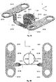
- FIG. 2A shows an isometric view of an articulated direct-mount inductor 201 configured to resolve the overheating issues associated with fasteners located within the high electromagnetic field, in accordance with some embodiments of the present invention.
- the articulated direct-mount inductor 201 is configured to directly mount to interfacing components without the use of separate connection straps, e.g., connection straps 186 and 188, and without the use of fasteners disposed within the high electromagnetic field emanating from the inductor 201, e.g., fasteners 191A and 191B.
- the articulated direct-mount inductor 201 can also be referred to as a fastener-free inductor 201, since there are no fasteners disposed within the high electromagnetic field emanating from the inductor 201.
- the articulated direct-mount inductor 201 is formed of electrically conductive material.
- the articulated direct-mount inductor 201 is formed of either copper, aluminum, electrically conductive alloy, or combination thereof, or of another type of electrically conductive material.
- the example articulated direct-mount inductor 201 of Figure 2A includes a coil portion 201A, a first articulation portion 201 B, a second articulation portion 201C, a first mounting structure 201D, and a second mounting structure 201E.
- the first mounting structure 201D includes a first mounting region 201G and a second mounting region 201F.
- the second mounting structure 201E includes a first mounting region 201H and a second mounting region 2011.
- Each of the mounting regions 201G, 201F, 201H, and 2011 is configured to mount in physical and electrical contact with a terminal of a respective electrical component, such as a variable capacitor.
- the articulated direct-mount inductor 201 includes four mounting regions 201G, 201F, 201H, and 2011 for connection to four electrical components
- the articulated direct-mount inductor 201 can be configured to connect to two or more electrical components, with the first mounting structure 201D including at least one mounting region and with the second mounting structure 201E including at least one mounting region.
- the first mounting structure 201D can include any number of mounting regions to accommodate physical and electrical connection to any corresponding number of electrical components.
- the second mounting structure 201E can include any number of mounting regions to accommodate physical and electrical connection to any corresponding number of electrical components.
- the articulated direct-mount inductor 201 includes a pivot section 201J configured to translate an orientation of the first mounting structure 201D relative to an orientation of a centerline 202 of the coil portion 201A. More specifically, the pivot section 201J in combination with a bend 201L orients the first mounting structure 201 D in the x-y plane, with the centerline 202 of the coil portion 201A oriented in the z-direction. It should be understood that in various embodiments, the pivot section 201J can be configured to position the first mounting structure 201D in essentially any desired orientation relative to the centerline 202 of the coil portion 201A.
- the articulated direct-mount inductor 201 includes a pivot section 201K configured to translate an orientation of the second mounting structure 201 E into the x-y plane, with the centerline 202 of the coil portion 201A oriented in the z-direction. It should be understood that in various embodiments, the pivot section 201K can be configured to position the second mounting structure 201E in essentially any desired orientation relative to the centerline 202 of the coil portion 201A.
- the first mounting structure 201D and the second mounting structure 201E are oriented to accommodate a required position and/or orientation of the electrical components to which they will connect, respectively, while the centerline 202 of the coil portion 201A is simultaneously oriented to provide for optimum cooling of the articulated direct-mount inductor 201.
- the centerline 202 of the coil portion 201A can be oriented in a predominate direction of cooling air flow to maximize an amount of cooling air flow through the coil portion 201A, while the first mounting structure 201D and the second mounting structure 201E are simultaneously oriented to accommodate a required position and/or orientation of the electrical components to which they will respectively connect.
- the articulated direct-mount inductor 201 is formed to have the pivot sections 201J and 201K positioned sufficiently far away from the centerline 202 of the coil portion 201A to ensure that geometric variation in the pivot sections 201J and 201K relative to the coil portion 201A does not cause an adverse perturbation in the inductance generated by the coil portion 201A.
- the articulated direct-mount inductor 201 is formed to have the pivot sections 201J and 201K positioned outside of a strong electromagnetic field emanating from the coil portion 201A.
- Figure 2B shows a top view of the articulated direct-mount inductor 201, in accordance with some embodiments of the present invention.
- Figure 2C shows a side view of the articulated direct-mount inductor 201, in accordance with some embodiments of the present invention.
- the coil portion 201A of the articulated direct-mount inductor 201 includes a number of turns of electrically conductive material about a core region having a diameter 201M.
- the diameter 201M of the core region of the coil portion 201A is within a range extending from about 0.5 inch to about 20 inches.
- the diameter 201M of the core region of the coil portion 201A is within a range extending from about 0.5 inch to about 10 inches.
- the diameter 201M of the core region of the coil portion 201A is within a range extending from about 1 inch to about 5 inches.
- the diameter 201M of the core region of the coil portion 201A is about 2.5 inches.
- the core region of the coil portion 201A is empty, i.e., is an air core region.
- the core region of the coil portion 201A can be occupied by a material suited for the intended operation of the articulated direct-mount inductor 201.
- the core region of the coil portion 201A can be occupied by a ceramic material or a polymer material, among other materials.
- the electrically conductive material that forms the coil portion 201A has a rectangular cross-section defined by a thickness 201N and a width 201P.
- the thickness 201N of the electrically conductive material that forms the coil portion 201A is within a range extending from about 0.032 inch to about 0.25 inch. In some embodiments, the thickness 201N of the electrically conductive material that forms the coil portion 201A is within a range extending from about 0.064 inch to about 0.25 inch. In some embodiments, the thickness 201N of the electrically conductive material that forms the coil portion 201A is within a range extending from about 0.125 inch to about 0.25 inch. In some embodiments, the thickness 201N of the electrically conductive material that forms the coil portion 201A is about 0.25 inch.
- the width 201P of the electrically conductive material that forms the coil portion 201A is within a range extending from about 0.125 inch to about 1.5 inches. In some embodiments, the width 201P of the electrically conductive material that forms the coil portion 201A is within a range extending from about 0.25 inch to about 1 inch. In some embodiments, the width 201P of the electrically conductive material that forms the coil portion 201A is within a range extending from about 0.5 inch to about 0.75 inch. In some embodiments, the width 201P of the electrically conductive material that forms the coil portion 201A is about 0.5 inch.
- adjacent turns of the electrically conductive material that forms the coil portion 201A are separated from each other by a distance 201O, as measured perpendicularly between facing side surfaces of the adjacent turns.
- the distance 201O between adjacent turns of the electrically conductive material that forms the coil portion 201A is within a range extending from about 0.125 inch to about 1 inch.
- the distance 201O between adjacent turns of the electrically conductive material that forms the coil portion 201A is within a range extending from about 0.125 inch to about 0.5 inch.
- the distance 201O between adjacent turns of the electrically conductive material that forms the coil portion 201A is within a range extending from about 0.125 inch to about 0.25 inch.
- the distance 201O between adjacent turns of the electrically conductive material that forms the coil portion 201A is about 0.125 inch.
- the coil portion 201A includes two complete turns about the core region having the diameter 201M.
- the coil portion 201A can include any number of turns and/or partial turns as needed to achieve a desired inductance value for a given frequency and power of radiofrequency signal(s) to be transmitted through the articulated direct-mount inductor 201.
- the number of turns of the coil portion 201A is within a range extending from 1 to 10.
- the number of turns of the coil portion 201A is within a range extending from 1 to 7.
- the number of turns of the coil portion 201A is within a range extending from 1 to 5.
- the number of turns of the coil portion 201A is 3.
- the diameter 201M, the thickness 201N, the width 201P, and the turn-to-turn spacing 201O can be defined as needed to achieve a desired inductance value for a given frequency and power of radiofrequency signal(s) to be transmitted through the articulated direct-mount inductor 201, while also satisfying any spatial installation requirements that may exist.
- the example articulated direct-mount inductor 201 of Figures 2A-2C has the coil portion 201A formed of the electrically conductive material of rectangular cross-section, it should be understood that in other embodiments the coil portion 201A can be formed of electrically conductive material of non-rectangular cross-section, such as of circular cross-section, oval cross-section, and/or other polygonal cross-section, among others.
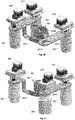
- FIG 3A shows the example articulated direct-mount inductor 201 of Figure 2A connected to four variable capacitors 301, 303, 305, and 307, in accordance with some embodiments of the present invention.
- Each of the four variable capacitors 301, 303, 305, and 307 is connected through mechanical linkage to a respective control motor 309, 111, 313, and 315.
- the four mounting regions 201G, 201F, 201H, and 2011 are configured to accommodate pass-through of the mechanical linkage from the control motors 309, 111, 313, 315 to the variable capacitors 301, 303, 305, 307, respectively.
- control motors 309, 111, 313, 315 and corresponding portions of the mechanical linkage are disposed within the electronics region 171 and the variable capacitors 301, 303, 305, 307 and corresponding portion of the mechanical linkage are disposed within the variable capacitors/inductor region 173 along with the articulated direct-mount inductor 201.
- Figure 3B shows the configuration of Figure 3A with the variable capacitor 305 and corresponding control motor 313 and associated mechanical linkage removed to reveal the mounting region 201H, in accordance with some embodiments of the present invention.
- the first and second mounting structures 201D, 201E of the articulated direct-mount inductor 201 are connected to the terminals of the variable capacitors 301, 303, 305, 307, as indicated in Figure 3A , using fasteners such as bolts or machine screws or the like.
- these fasteners are formed of the same material as the articulated direct-mount inductor 201 to ensure consistency in coefficients of thermal expansion to avoid shearing of the fasteners.
- the first and second mounting structures 201D, 201E of the articulated direct-mount inductor 201 are connected to the terminals of the variable capacitors 301, 303, 305, 307, as indicated in Figure 3A , using a clamping force applied by mechanical clamping structures separate from the articulated direct-mount inductor 201.
- the fasteners and/or mechanical clamping structures used to connect the first and second mounting structures 201D, 201E of the articulated direct-mount inductor 201 to the terminals of the variable capacitors 301, 303, 305, 307 are located outside of the strong electromagnetic field emanating from the coil portion 201A during operation. Therefore, it should be understood and appreciated that these fasteners and/or mechanical clamping structures will not be subject to excessive heating induced by the strong electromagnetic field emanating from the coil portion 201A during operation.
- the articulated direct-mount inductor 201 can be configured to connect to two or more electrical components, with the first mounting structure 201D connected to at least one electrical component and with the second mounting structure 201E connected to at least one electrical component.
- Figure 4 shows an example of the articulated direct-mount inductor 201 configured to connect to three variable capacitors 301, 305, and 307, in accordance with some embodiments of the present invention.
- a mounting structure 401 replaces the first mounting structure 201D as depicted in the example of Figures 2A-2C .
- the mounting structure 401 is configured to connect to one electrical component, e.g., to the variable capacitor 301.
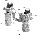
- Figure 5 shows another example of the articulated direct-mount inductor 201 configured to connect to two variable capacitors 301 and 305, in accordance with some embodiments of the present invention.
- the mounting structure 401 is present for connection to one electrical component, e.g., to the variable capacitor 301.
- a mounting structure 501 replaces the second mounting structure 201E as depicted in the example of Figures 2A-2C .
- the mounting structure 501 is configured to connect to one electrical component, e.g., to the variable capacitor 305.
- the articulated direct-mount inductor 201 configurations as shown in Figures 2A-2C , 4 , and 5 are provided by way of example to facilitate description of the present invention.
- the articulated direct-mount inductor 201 can be configured different from what is shown in the examples of Figures 2A-2C , 4 , and 5 .
- one or both of the first mounting structure 201D and the second mounting structure 201E can be configured to connect with three or more electrical components.
- one or both of the first mounting structure 201D and the second mounting structure 201E can be configured to include one or more bends and multiple portions that have different spatial orientations.
- one or both of the first mounting structure 201 D and the second mounting structure 201E can include a first portion oriented in the x-y plane and a second portion oriented in the x-z plane, with a bend between the first portion and the second portion.
- one or both of the first mounting structure 201D and the second mounting structure 201E can include a first portion oriented in the x-y plane and a second portion oriented in the x-z plane and a third portion oriented in the y-z plane, with a first bend between the first portion and the second portion and with a second bend between the second portion and the third portion.
- each of the first mounting structure 201D and the second mounting structure 201E can have essentially any spatial configuration as needed to accommodate connection to essentially any number of electrical components having essentially any spatial orientation.
- the articulated direct-mount inductor 201 is a one-piece inductor configuration that can connect directly with multiple electrical components at different locations within an impedance matching system.
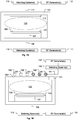
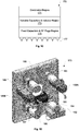
- FIG. 6 shows a flowchart of a method for configuring an impedance matching system, in accordance with some embodiments of the present invention.
- the method includes an operation 601 for providing an articulated direct-mount inductor configured to directly connect to at least two electrical components at respective locations outside of a strong electromagnetic field emanating from a coil portion of the articulated direct-mount inductor during operation.
- the at least two electrical components include one or more variable capacitors and/or one or more fixed capacitors.
- the articulated direct-mount inductor includes a first articulation portion extending from the coil portion to a first mounting portion and a second articulation portion extending from the coil portion to a second mounting structure.
- the method also includes an operation 603 for connecting the articulated direct-mount inductor directly to the at least two electrical components.
- the articulated direct-mount inductor is connected to each of the at least two electrical components without use of connection straps formed separate from the articulated direct-mount inductor.
- any fasteners used to connect the articulated direct-mount inductor to the at least two electrical components are located outside of the strong electromagnetic field emanating from the coil portion of the articulated direct-mount inductor during operation.
- the operations 601 and 603 are performed such that a centerline of the coil portion of the articulated direct-mount inductor is oriented in a direction of a predominate cooling air flow path through the impedance matching system.
- the articulated direct-mount inductor 201 can be formed using various metal fabrication processes.
- an entirety of the articulated direct-mount inductor 201 (including the coil portion 201A, the first articulation portion 201B, the second articulation portion 201C, the first mounting structure 201D, and the second mounting structure 201E) is laid out on a planar sheet of electrically conductive material, e.g., metal.
- the articulated direct-mount inductor 201 in its planar form is cut out of the planar sheet of electrically conductive material, such as by laser cutting and/or water jet cutting and/or drilling and/or other type of metal fabrication process.
- the articulated direct-mount inductor 201 is transformed from its planar state into its final three-dimensional form through use of various bending processes, twisting processes, and coil wrapping processes, as needed.
- FIG. 7 shows a flowchart of a method for manufacturing an articulated direct-mount inductor, in accordance with some embodiments of the present invention.
- the method includes an operation 701 for laying out an entirety of the articulated direct-mount inductor in a planar form on a planar sheet of electrically conductive material.
- the articulated direct-mount inductor in its planar form includes a rectangular-shaped region, and a first mounting structure region located at a first end of the rectangular-shaped region, and a second mounting structure region located at a second end of the rectangular-shaped region.
- the method includes an operation 703 for cutting out the entirety of the articulated direct-mount inductor in its planar form from the planar sheet of electrically conductive material.
- the cutting of operation 703 can include one or more of laser cutting, water jet cutting, and drilling, among other fabrication techniques/processes.
- the method includes an operation 705 for wrapping a portion of the rectangular-shaped region of the articulated direct-mount inductor in its planar form around a core formation structure to form a helical-shaped coil portion.
- the core formation structure is cylindrical in shape, such that operation 705 results in transformation of the portion of the rectangular-shaped region of the articulated direct-mount inductor into a circular helical-shaped coil portion, such as the coil portion 201A shown in Figure 2A .
- the core formation structure can have a non-cylindrical shape.
- the core formation structure can be shaped as a rectangular parallelepiped, such that operation 705 results in transformation of the portion of the rectangular-shaped region of the articulated direct-mount inductor into a rectangular helical-shaped coil portion.
- the core formation structure can have essentially any three-dimensional shape that is suitable to be wrapped by the portion of the rectangular-shaped region of the articulated direct-mount inductor in its planar form to create a helical-shaped coil portion.
- the method also includes an operation 707 for removing the core formation structure from within the helical-shaped coil portion.
- the method also includes an operation 709 for bending a portion of the articulated direct-mount inductor in its planar form between the helical-shaped coil portion and the first mounting structure region to form a first articulation portion, such as the first articulation portion 201B shown in Figure 2A .
- the method also includes an operation 711 for bending a portion of the articulated direct-mount inductor in its planar form between the helical-shaped coil portion and the second mounting structure region to form a second articulation portion, such as the second articulation portion 201C shown in Figure 2A .
- the first articulation portion and the second articulation portion are formed to enable connection of the first mounting structure and the second mounting structure, respectively, to electrical components to which the articulated direct-mount inductor directly interfaces.
- the method can also include an operation for twisting the articulated direct-mount inductor in its planar form when forming one or both of the first articulation portion and the second articulation portion to offset a centerline of the helical-shaped coil portion from one or both of the first mounting structure region and the second mounting structure region.
- the centerline of the helical-shaped coil portion is offset in an orthogonal relationship from plane(s) within which the first mounting structure region and the second mounting structure region reside.
- the conventional inductor 181 is a stock component fabricated without full consideration of its end-use installation. As such, the conventional inductor 181 requires connection straps 186, 188 and associated fasteners 191A, 191B to connect with electrical components in its end-use installation. And, the locations of the fasteners 191A, 191B within the strong electromagnetic field emanating from the conventional inductor 181 cause excessive and damaging heating of the conventional inductor 181 and interfacing components.
- the articulated direct-mount inductor 201 disclosed herein extends in an articulated manner to connect directly with interfacing electrical components, and therefore does not require use of connection straps, e.g., connection straps 186, 188, and associated fasteners, e.g., fasteners 191A, 191B.
- connection straps e.g., connection straps 186, 188
- associated fasteners e.g., fasteners 191A, 191B.
- fasteners 191A, 191B there are no fasteners located within the strong electromagnetic field emanating from the coil portion 201A of the articulated direct-mount inductor 201, and hence no excessive and damaging heating of such fasteners.
- connection of the articulated direct-mount inductor 201 directly to its interfacing electrical components occurs outside of the strong electromagnetic field emanating from the coil portion 201A of the articulated direct-mount inductor 201.
- any fasteners used to connect the articulated direct-mount inductor 201 directly to its interfacing electrical components will be located outside of the strong electromagnetic field emanating from the coil portion 201A of the articulated direct-mount inductor 201 and will not be subject to excessive and damaging heating.
- a temperature of the articulated direct-mount inductor 201 will be within a range extending from about 25 °C to about 150 °C during operation, which is within an acceptable temperature range for air cooled impedance matching systems.
- a temperature of the articulated direct-mount inductor 201 will be less than 100 °C during operation, which is within an acceptable temperature range for air cooled impedance matching systems.
- the articulated direct-mount inductor 201 reduces the number of required parts from seven to one, which reduces cost and simplifies inductor installation within the impedance matching system.
Landscapes
- Engineering & Computer Science (AREA)
- Power Engineering (AREA)
- Manufacturing & Machinery (AREA)
- Physics & Mathematics (AREA)
- Plasma & Fusion (AREA)
- Chemical & Material Sciences (AREA)
- Analytical Chemistry (AREA)
- Coils Or Transformers For Communication (AREA)
- Plasma Technology (AREA)
Abstract
Description
- The present invention relates to semiconductor device fabrication.
- In various semiconductor fabrication processes, radiofrequency power is transmitted to a processing chamber to generate plasma and/or generate bias voltage and/or produce some other desired effect. The radiofrequency power is generated by a radiofrequency power supply and is transmitted through an impedance matching system in route to the processing chamber. Generally speaking, the impedance matching system is configured to ensure that a load impedance seen by the radiofrequency power supply is sufficient close to a load impedance for which the radiofrequency power supply is designed, so that radiofrequency power will be efficiently transmitted to the load within the processing chamber without unacceptable radiofrequency signal reflection and/or loss. Transmission of the radiofrequency power through the impedance matching system can cause heating of components within the impedance matching system that must be managed to avoid thermally-induced damage. It is within this context that the present invention arises.
- In an example embodiment, an articulated direct-mount inductor is disclosed. The articulated direct-mount inductor includes a coil portion of an electrically conductive material. The articulated direct-mount inductor also includes a first articulation portion of the electrically conductive material extending from the coil portion. The articulated direct-mount inductor also includes a first mounting structure of the electrically conductive material extending from the first articulation portion. The first mounting structure includes a first mounting region configured to mount in physical and electrical contact with a terminal of a first electrical component. The first articulation portion and the first mounting structure are collectively configured to position the first mounting region at a location outside of a strong electromagnetic field emanating from the coil portion when radiofrequency power is transmitted through the articulated direct-mount inductor. The articulated direct-mount inductor also includes a second articulation portion of the electrically conductive material extending from the coil portion. The articulated direct-mount inductor also includes a second mounting structure of the electrically conductive material extending from the second articulation portion. The second mounting structure includes a second mounting region configured to mount in physical and electrical contact with a terminal of a second electrical component. The second articulation portion and the second mounting structure are collectively configured to position the second mounting region at a location outside of the strong electromagnetic field emanating from the coil portion when radiofrequency power is transmitted through the articulated direct-mount inductor.
- In an example embodiment, a method is disclosed for configuring an impedance matching system. The method includes providing an articulated direct-mount inductor configured to directly connect to at least two electrical components at respective locations outside of a strong electromagnetic field emanating from a coil portion of the articulated direct-mount inductor when radiofrequency power is transmitted through the articulated direct-mount inductor. The articulated direct-mount inductor includes a first articulation portion extending from the coil portion to a first mounting portion. The articulated direct-mount inductor also includes a second articulation portion extending from the coil portion to a second mounting structure. The method also includes connecting the articulated direct-mount inductor directly to the at least two electrical components.
- In an example embodiment, a method is disclosed for manufacturing an articulated direct-mount inductor. The method includes laying out an entirety of the articulated direct-mount inductor in a planar form on a planar sheet of electrically conductive material. The articulated direct-mount inductor in its planar form includes a rectangular-shaped region, and a first mounting structure region located at a first end of the rectangular-shaped region, and a second mounting structure region located at a second end of the rectangular-shaped region. The method also includes cutting out the entirety of the articulated direct-mount inductor in its planar form from the planar sheet of electrically conductive material. The method also includes wrapping a portion of the rectangular-shaped region of the articulated direct-mount inductor in its planar form around a core formation structure to form a helical-shaped coil portion. The method also includes removing the core formation structure from within the helical-shaped coil portion. The method also includes bending a portion of the articulated direct-mount inductor in its planar form between the helical-shaped coil portion and the first mounting structure region to form a first articulation portion. The method also includes bending a portion of the articulated direct-mount inductor in its planar form between the helical-shaped coil portion and the second mounting structure region to form a second articulation portion. The first articulation portion and the second articulation portion are formed to enable connection of the first mounting structure and the second mounting structure, respectively, to electrical components to which the articulated direct-mount inductor directly interfaces.
- Other aspects and advantages of the invention will become more apparent from the following detailed description, taken in conjunction with the accompanying drawings, illustrating by way of example the present invention.
-
-
Figure 1A shows an example vertical cross-section diagram of a CCP processing chamber, in accordance with some embodiments of the present invention. -
Figure 1B shows an example vertical cross-section diagram of an ICP processing chamber, in accordance with some embodiments of the present invention. -
Figure 1C shows a configuration of an example impedance matching system, in accordance with some embodiments of the present invention. -
Figure 1D shows an example configuration of the variable capacitors and inductor region, including a radiofrequency signal supply input terminal. -
Figure 1E shows a closer view of the mechanical/electrical connection between the second terminal of the variable capacitor and a first connection region at the first end of the conventional inductor, through the connection strap. -
Figure 1F shows a closer view of the mechanical/electrical connection between a second connection region of the conventional inductor and each of the first terminal of the variable capacitor and the first terminal of the variable capacitor, through the connection strap. -
Figure 1G shows an isometric view of the conventional inductor. -
Figure 1H shows a configuration of the substantially rectangular-shaped electrically conductive material prior to it being wound into the coil to form the conventional inductor. -
Figure 1I shows the conventional inductor with lines depicting the strong electromagnetic field generated by transmission of radiofrequency signal(s) through the conventional inductor. -
Figure 2A shows an isometric view of an articulated direct-mount inductor configured to resolve the overheating issues associated with fasteners located within the high electromagnetic field, in accordance with some embodiments of the present invention. -
Figure 2B shows a top view of the articulated direct-mount inductor, in accordance with some embodiments of the present invention. -
Figure 2C shows a side view of the articulated direct-mount inductor, in accordance with some embodiments of the present invention. -
Figure 3A shows the example articulated direct-mount inductor ofFigure 2A connected to four variable capacitors, in accordance with some embodiments of the present invention. -
Figure 3B shows the configuration ofFigure 3A with the variable capacitor and corresponding control motor and associated mechanical linkage removed to reveal the mounting region, in accordance with some embodiments of the present invention. -
Figure 4 shows an example of the articulated direct-mount inductor configured to connect to three variable capacitors, in accordance with some embodiments of the present invention. -
Figure 5 shows another example of the articulated direct-mount inductor configured to connect to two variable capacitors, in accordance with some embodiments of the present invention. -
Figure 6 shows a flowchart of a method for configuring an impedance matching system, in accordance with some embodiments of the present invention. -
Figure 7 shows a flowchart of a method for manufacturing an articulated direct-mount inductor, in accordance with some embodiments of the present invention. - In the following description, numerous specific details are set forth in order to provide a thorough understanding of the present invention. It will be apparent, however, to one skilled in the art that the present invention may be practiced without some or all of these specific details. In other instances, well known process operations have not been described in detail in order not to unnecessarily obscure the present invention.
- In the semiconductor industry, semiconductor substrates can undergo fabrication operations in various types of plasma chambers, such as capacitively coupled plasma (CCP) processing chamber and inductively coupled plasma (ICP) plasma processing chambers.
Figure 1A shows an example vertical cross-section diagram of aCCP processing chamber 101, in accordance with some embodiments of the present invention. TheCCP processing chamber 101 defines a processing volume within which aplasma 123 is generated in exposure to asubstrate 105 to affect a change to thesubstrate 105 in a controlled manner. In various fabrication processes, the change to thesubstrate 105 can be a change in material or surface condition on thesubstrate 105. For example, in various fabrication processes, the change to thesubstrate 105 can include one or more of etching of a material from thesubstrate 105, deposition of a material on thesubstrate 105, or modification ofmaterial 105 present on thesubstrate 105. - In some embodiments, the
substrate 105 is a semiconductor wafer undergoing a fabrication procedure. However, it should be understood that in various embodiments, thesubstrate 105 can be essentially any type of substrate that is subjected to a plasma-based fabrication process. For example, in some embodiments, theterm substrate 105 as used herein can refer to substrates formed of sapphire, GaN, GaAs or SiC, or other substrate materials, and can include glass panels/substrates, metal foils, metal sheets, polymer materials, or the like. Also, in various embodiments, thesubstrate 105 as referred to herein may vary in form, shape, and/or size. For example, in some embodiments, thesubstrate 105 referred to herein may correspond to a 200 mm (millimeters) semiconductor wafer, a 300 mm semiconductor wafer, or a 450 mm semiconductor wafer. Also, in some embodiments, thesubstrate 105 referred to herein may correspond to a non-circular substrate, such as a rectangular substrate for a flat panel display, or the like, among other shapes. - In various embodiments, the
CCP processing chamber 101 operates by flowing one or more process gases into the processing volume, and by applying radiofrequency power to the one or more process gases to transform the one or more process gases into theplasma 123 in exposure to thesubstrate 105, in order to affect a change in material or surface condition on thesubstrate 105. TheCCP processing chamber 101 includes asubstrate support structure 103 upon which thesubstrate 105 is positioned and supported during processing operations. In some embodiments, anelectrode 107 is disposed within thesubstrate support structure 103 to provide for transmission of radiofrequency power from theelectrode 107 through the processing volume to generate theplasma 123. Theelectrode 107 is connected to receive radiofrequency power through a radiofrequencypower supply structure 109, which is connected to one or more radiofrequency signal generator(s) 111 by way of one or more impedance matching system(s) 113. The matching system(s) 113 include an arrangement of capacitors and inductors configured to ensure that an impedance seen by the radiofrequency signal generator(s) 111 at the radiofrequencypower supply structure 109 is sufficiently close to a load impedance for which the radiofrequency signal generator(s) 111 is designed to operate, so that radiofrequency signals generated and transmitted by the radiofrequency signal generator(s) 111 will be transmitted into the processing volume in an efficient manner, i.e., without unacceptable reflection. - Also, in some embodiments, an
upper electrode 115 can also be provided. In various embodiments, theupper electrode 115 can provide either an electrical ground electrode or can be used to transmit radiofrequency power into the processing volume. In some embodiments, theupper electrode 115 is connected to receive radiofrequency power through a radiofrequencypower supply structure 117, which is connected to one or more radiofrequency signal generator(s) 121 by way of one or more impedance matching system(s) 119. The matching system(s) 119 include an arrangement of capacitors and inductors configured to ensure that an impedance seen by the radiofrequency signal generator(s) 121 at the radiofrequencypower supply structure 117 is sufficiently close to a load impedance for which the radiofrequency signal generator(s) 121 is designed to operate, so that radiofrequency signals generated and transmitted by the radiofrequency signal generator(s) 121 will be transmitted into the processing volume in an efficient manner, i.e., without unacceptable reflection. -
Figure 1B shows an example vertical cross-section diagram of anICP processing chamber 151, in accordance with some embodiments of the present invention. The ICP processing chamber can also be referred to as a transformer coupled plasma (TCP) processing chamber. For ease of discussion herein, ICP processing chamber will be used to refer to both ICP and TCP processing chambers. TheICP processing chamber 151 defines a processing volume within which theplasma 123 is generated in exposure to thesubstrate 105 to affect a change to thesubstrate 105 in a controlled manner. In various fabrication processes, the change to thesubstrate 105 can be a change in material or surface condition on thesubstrate 105. For example, in various fabrication processes, the change to thesubstrate 105 can include one or more of etching of a material from thesubstrate 105, deposition of a material on thesubstrate 105, or modification ofmaterial 105 present on thesubstrate 105. - It should be understood that the ICP processing chamber 150 can be any type of ICP processing chamber in which radiofrequency signals are transmitted from a
coil 155 disposed outside theICP processing chamber 151 to a process gas within theICP processing chamber 151 to generate theplasma 123 within theICP processing chamber 151. Anupper window structure 153 is provided to allow for transmission of radiofrequency signals from thecoil 155 through theupper window structure 153 and into the processing volume of theICP processing chamber 151. The ICP processing chamber 150 operates by flowing one or more process gases into the processing volume, and by applying radiofrequency power from thecoil 155 to the one or more process gases to transform the one or more process gases into theplasma 123 in exposure to thesubstrate 105, in order to affect a change in material or surface condition on thesubstrate 105. Thecoil 155 is disposed above theupper window structure 153. In the example ofFigure 1B , thecoil 155 is formed as a radial coil assembly, with the shaded parts of thecoil 155 turning into the page of the drawing and with the unshaded parts of thecoil 155 turning out of the page of the drawing. It should be understood, however, that in other embodiments thecoil 155 can be of essentially any configuration that is suitable for transmitting radiofrequency power through theupper window structure 153 and into the plasma processing volume. In various embodiments, thecoil 155 can have any number of turns and any cross-section size and shape (circular, oval, rectangular, trapezoidal, etc.) as required to provide the necessary transmission of radiofrequency signals through theupper window structure 153 into the processing volume. - The
coil 155 is connected through a radiofrequencypower supply structure 161 to one or more radiofrequency signal generator(s) 157 by way of one or more matching system(s) 159. The matching system(s) 159 includes an arrangement of capacitors and/or inductors configured to ensure that an impedance seen by the radiofrequency signal generator(s) 157 at thecoil 155 is sufficiently close to a load impedance for which the radiofrequency signal generator(s) 157 is designed to operate, so that radiofrequency signals supplied to thecoil 155 by the primary radiofrequency signal generator(s) 157 will be transmitted into the processing volume in an efficient manner, i.e., without unacceptable reflection. Also, in some embodiments, theICP processing chamber 151 can include theelectrode 107, the radiofrequencypower supply structure 109, the matching system(s) 113, and the radiofrequency signal generator(s) 111, as previously described with regard toFigure 1A . -
Figure 1C shows a configuration of an exampleimpedance matching system 170, in accordance with some embodiments of the present invention. The exampleimpedance matching system 170 can be used for any of thematching systems Figures 1A and 1B . Theimpedance matching system 170 includes anelectronics region 171 that includes control boards, cables, and server motors for controlling settings of variable capacitors. Theimpedance matching system 170 also includes a variable capacitors/inductor region 173 that includes a number of variable capacitors positioned and connected to be controlled by the sever motors within theelectronics region 171. The variable capacitors/inductor region 173 also includes at least one inductor connected to electrical components, such as to a number of the variable capacitors. The variable capacitors/inductor region 173 can also include a number of voltage-current (VI) sensors and corresponding connection structures. Theimpedance matching system 170 includes a fixed capacitors/radiofrequency plugsregion 175 that includes a number of fixed capacitors and a number of radiofrequency plugs 177 configured to provide for electrical connection to the chamber coil(s) and/or electrode(s). - It should be understood that the various components disposed within the example
impedance matching system 170 are connected to form an impedance matching circuit that functions to substantially match an impedance of the load, i.e., of theplasma 123, to an impedance of the radiofrequency signal source, i.e., to the impedance of the radiofrequency signal generator(s) 121, 111, 157, so that radiofrequency power will be efficiently transferred to the load. It should be understood that the configuration of the exampleimpedance matching system 170 discussed above is provided to facilitate description of the present invention and is not intended to be limiting. In other embodiments, the invention disclosed herein can be used with essentially any impedance matching system configuration. -
Figure 1D shows an example configuration of the variable capacitors/inductor region 173, including a radiofrequency signalsupply input terminal 182. Also, in this example, the variable capacitors/inductor region 173 includesmultiple VI sensors variable capacitor 184. A second terminal of thevariable capacitor 184 is connected to a first terminal of avariable capacitor 187. A second terminal of thevariable capacitor 187 is connected to a first end of aconventional inductor 181, through aconnection strap 186.Figure 1E shows a closer view of the mechanical/electrical connection between the second terminal of thevariable capacitor 187 and afirst connection region 181A at the first end of theconventional inductor 181, through theconnection strap 186. Thefirst connection region 181A of theconventional inductor 181 includes a pair of holes to accommodatefasteners 191A for securing theconventional inductor 181 to theconnection strap 186. -
Figure 1D also shows a second terminal of theconventional inductor 181 connected to both a first terminal of avariable capacitor 183 and a first terminal of avariable capacitor 185, through aconnection strap 188.Figure 1F shows a closer view of the mechanical/electrical connection between asecond connection region 181B of theconventional inductor 181 and each of the first terminal of thevariable capacitor 183 and the first terminal of thevariable capacitor 185, through theconnection strap 188. Thesecond connection region 181B of theconventional inductor 181 includes a pair of holes to accommodatefasteners 191B for securing theconventional inductor 181 to theconnection strap 188. - It should be understood that the variable capacitors/
inductor region 173 can include more or less components than those discussed above. However, attention is drawn to the configuration of theconventional inductor 181 and the connection straps 186 and 188 used to connect theconventional inductor 181 to thevariable capacitors Figure 1G shows an isometric view of theconventional inductor 181. Theconventional inductor 181 is formed as a simple coil of electrically conductive material. For instance,Figure 1H shows a configuration of electrically conductive material 181' prior to it being wound into the coil to form theconventional inductor 181.Figure 1I shows theconventional inductor 181 withlines 193 depicting the strong electromagnetic field generated by transmission of radiofrequency signal(s) through theconventional inductor 181. As shown inFigure 1I , thefirst connection region 181A and thesecond connection region 181B of theconventional inductor 181 are positioned within the strong electromagnetic field emanating from theconventional inductor 181. - The strong electromagnetic field emanating from the
conventional inductor 181 causes heating of thefasteners 191A within thefirst connection region 181A of theconventional inductor 181 and heating of thefasteners 191B within thesecond connection region 181B of theconventional inductor 181. Thefasteners conventional inductor 181 to the connection straps 186 and 188 are formed of a material that is chemically and mechanically compatible with both theconventional inductor 181 and the connection straps 186 and 188. In some cases, thefasteners conventional inductor 181, e.g., copper, aluminum, etc., so as to match the coefficient of thermal expansion between thefasteners conventional inductor 181. Otherwise, thefasteners conventional inductor 181 heats up and expands dimensionally. Similarly, in some cases, the connection straps 186 and 188 are also formed of the same material as thefasteners conventional inductor 181 to avoid incompatible coefficients of thermal expansion. - By way of example, in some embodiments, based on a 97% efficiency, about 200 Watts (W) may be dissipated in the variable capacitors/
inductor region 173 of the exampleimpedance matching system 170. And, a majority of this power will be dissipated from theconventional inductor 181. In some embodiments, a fan is installed to provide forced air cooling through theimpedance matching system 170, and especially through the variable capacitors/inductor region 173. However, the forced air cooling is not capable of removing the excess heat from within the variable capacitors/inductor region 173. During operation, theconventional inductor 181 can reach temperatures up to 300 °C, making theconventional inductor 181 glow red hot, and even anneal in some cases. Even with maximum cooling effort, the excessively high temperature of theconventional inductor 181 cannot be sufficiently reduced. In an effort to reduce the operating temperature of theconventional inductor 181, a lower inductance version of theconventional inductor 181 can be tried. However, the lower inductance version of theconventional inductor 181 in combination with maximum forced air cooling may only reduce the temperature of theconventional inductor 181 to about 150 °C, with is still too high. - Infrared analysis of the operating
impedance matching system 170 indicates that thefasteners conventional inductor 181. Prior to the present invention, it was an industry standard practice to specify theconventional inductor 181 as an individual component formed as a simple coil of electrically conductive material, in combination with specification ofseparate connection straps conventional inductor 181 and other components within theimpedance matching system 170. Also, prior to the present invention, the available industry standardconventional inductors 181 had theirfirst connection region 181A andsecond connection region 181B located proximate to the coiled region (such as shown inFigure 1G ) such that changing from oneconventional inductor 181 to another would not cure the overheating issue caused by thefasteners conventional inductor 181 during operation. Because of theconventional inductor 181 being an off-the-shelf spec component, and because of an aversion to modifying the configuration of other components within theimpedance matching system 170, prior attempts at managing the excessive heating issue within theimpedance matching system 170 focused on cooling methods. However, the cooling methods were determined to be insufficient for lowering the temperature of thefasteners overheated fasteners -
Figure 2A shows an isometric view of an articulated direct-mount inductor 201 configured to resolve the overheating issues associated with fasteners located within the high electromagnetic field, in accordance with some embodiments of the present invention. The articulated direct-mount inductor 201 is configured to directly mount to interfacing components without the use of separate connection straps, e.g., connection straps 186 and 188, and without the use of fasteners disposed within the high electromagnetic field emanating from theinductor 201, e.g.,fasteners mount inductor 201 can also be referred to as a fastener-free inductor 201, since there are no fasteners disposed within the high electromagnetic field emanating from theinductor 201. The articulated direct-mount inductor 201 is formed of electrically conductive material. In various embodiments, the articulated direct-mount inductor 201 is formed of either copper, aluminum, electrically conductive alloy, or combination thereof, or of another type of electrically conductive material. - The example articulated direct-
mount inductor 201 ofFigure 2A includes acoil portion 201A, afirst articulation portion 201 B, asecond articulation portion 201C, afirst mounting structure 201D, and asecond mounting structure 201E. Thefirst mounting structure 201D includes a first mountingregion 201G and asecond mounting region 201F. Similarly, thesecond mounting structure 201E includes a first mountingregion 201H and asecond mounting region 2011. Each of the mountingregions mount inductor 201 includes four mountingregions mount inductor 201 can be configured to connect to two or more electrical components, with thefirst mounting structure 201D including at least one mounting region and with thesecond mounting structure 201E including at least one mounting region. Also, it should be understood that in various embodiments, thefirst mounting structure 201D can include any number of mounting regions to accommodate physical and electrical connection to any corresponding number of electrical components. And, similarly, in various embodiments, thesecond mounting structure 201E can include any number of mounting regions to accommodate physical and electrical connection to any corresponding number of electrical components. - In the example of
Figure 2A , the articulated direct-mount inductor 201 includes apivot section 201J configured to translate an orientation of thefirst mounting structure 201D relative to an orientation of acenterline 202 of thecoil portion 201A. More specifically, thepivot section 201J in combination with abend 201L orients thefirst mounting structure 201 D in the x-y plane, with thecenterline 202 of thecoil portion 201A oriented in the z-direction. It should be understood that in various embodiments, thepivot section 201J can be configured to position thefirst mounting structure 201D in essentially any desired orientation relative to thecenterline 202 of thecoil portion 201A. Similarly, the articulated direct-mount inductor 201 includes apivot section 201K configured to translate an orientation of thesecond mounting structure 201 E into the x-y plane, with thecenterline 202 of thecoil portion 201A oriented in the z-direction. It should be understood that in various embodiments, thepivot section 201K can be configured to position thesecond mounting structure 201E in essentially any desired orientation relative to thecenterline 202 of thecoil portion 201A. In some embodiments, thefirst mounting structure 201D and thesecond mounting structure 201E are oriented to accommodate a required position and/or orientation of the electrical components to which they will connect, respectively, while thecenterline 202 of thecoil portion 201A is simultaneously oriented to provide for optimum cooling of the articulated direct-mount inductor 201. For example, in some embodiments, thecenterline 202 of thecoil portion 201A can be oriented in a predominate direction of cooling air flow to maximize an amount of cooling air flow through thecoil portion 201A, while thefirst mounting structure 201D and thesecond mounting structure 201E are simultaneously oriented to accommodate a required position and/or orientation of the electrical components to which they will respectively connect. Also, in some embodiments, the articulated direct-mount inductor 201 is formed to have thepivot sections centerline 202 of thecoil portion 201A to ensure that geometric variation in thepivot sections coil portion 201A does not cause an adverse perturbation in the inductance generated by thecoil portion 201A. In some embodiments, the articulated direct-mount inductor 201 is formed to have thepivot sections coil portion 201A. -
Figure 2B shows a top view of the articulated direct-mount inductor 201, in accordance with some embodiments of the present invention.Figure 2C shows a side view of the articulated direct-mount inductor 201, in accordance with some embodiments of the present invention. Thecoil portion 201A of the articulated direct-mount inductor 201 includes a number of turns of electrically conductive material about a core region having adiameter 201M. In some embodiments, thediameter 201M of the core region of thecoil portion 201A is within a range extending from about 0.5 inch to about 20 inches. In some embodiments, thediameter 201M of the core region of thecoil portion 201A is within a range extending from about 0.5 inch to about 10 inches. In some embodiments, thediameter 201M of the core region of thecoil portion 201A is within a range extending from about 1 inch to about 5 inches. In some embodiments, thediameter 201M of the core region of thecoil portion 201A is about 2.5 inches. - In some embodiments, the core region of the
coil portion 201A is empty, i.e., is an air core region. However, in other embodiments, the core region of thecoil portion 201A can be occupied by a material suited for the intended operation of the articulated direct-mount inductor 201. For example, in some embodiments, the core region of thecoil portion 201A can be occupied by a ceramic material or a polymer material, among other materials. In some embodiments, the electrically conductive material that forms thecoil portion 201A has a rectangular cross-section defined by athickness 201N and awidth 201P. In some embodiments, thethickness 201N of the electrically conductive material that forms thecoil portion 201A is within a range extending from about 0.032 inch to about 0.25 inch. In some embodiments, thethickness 201N of the electrically conductive material that forms thecoil portion 201A is within a range extending from about 0.064 inch to about 0.25 inch. In some embodiments, thethickness 201N of the electrically conductive material that forms thecoil portion 201A is within a range extending from about 0.125 inch to about 0.25 inch. In some embodiments, thethickness 201N of the electrically conductive material that forms thecoil portion 201A is about 0.25 inch. In some embodiments, thewidth 201P of the electrically conductive material that forms thecoil portion 201A is within a range extending from about 0.125 inch to about 1.5 inches. In some embodiments, thewidth 201P of the electrically conductive material that forms thecoil portion 201A is within a range extending from about 0.25 inch to about 1 inch. In some embodiments, thewidth 201P of the electrically conductive material that forms thecoil portion 201A is within a range extending from about 0.5 inch to about 0.75 inch. In some embodiments, thewidth 201P of the electrically conductive material that forms thecoil portion 201A is about 0.5 inch. - Also, in some embodiments, adjacent turns of the electrically conductive material that forms the
coil portion 201A are separated from each other by a distance 201O, as measured perpendicularly between facing side surfaces of the adjacent turns. In some embodiments, the distance 201O between adjacent turns of the electrically conductive material that forms thecoil portion 201A is within a range extending from about 0.125 inch to about 1 inch. In some embodiments, the distance 201O between adjacent turns of the electrically conductive material that forms thecoil portion 201A is within a range extending from about 0.125 inch to about 0.5 inch. In some embodiments, the distance 201O between adjacent turns of the electrically conductive material that forms thecoil portion 201A is within a range extending from about 0.125 inch to about 0.25 inch. In some embodiments, the distance 201O between adjacent turns of the electrically conductive material that forms thecoil portion 201A is about 0.125 inch. - In the example of
Figures 2A-2C , thecoil portion 201A includes two complete turns about the core region having thediameter 201M. However, it should be understood that in other embodiments, thecoil portion 201A can include any number of turns and/or partial turns as needed to achieve a desired inductance value for a given frequency and power of radiofrequency signal(s) to be transmitted through the articulated direct-mount inductor 201. In some embodiments, the number of turns of thecoil portion 201A is within a range extending from 1 to 10. In some embodiments, the number of turns of thecoil portion 201A is within a range extending from 1 to 7. In some embodiments, the number of turns of thecoil portion 201A is within a range extending from 1 to 5. In some embodiments, the number of turns of thecoil portion 201A is 3. - Also, in various embodiments, the
diameter 201M, thethickness 201N, thewidth 201P, and the turn-to-turn spacing 201O can be defined as needed to achieve a desired inductance value for a given frequency and power of radiofrequency signal(s) to be transmitted through the articulated direct-mount inductor 201, while also satisfying any spatial installation requirements that may exist. Additionally, while the example articulated direct-mount inductor 201 ofFigures 2A-2C has thecoil portion 201A formed of the electrically conductive material of rectangular cross-section, it should be understood that in other embodiments thecoil portion 201A can be formed of electrically conductive material of non-rectangular cross-section, such as of circular cross-section, oval cross-section, and/or other polygonal cross-section, among others. -
Figure 3A shows the example articulated direct-mount inductor 201 ofFigure 2A connected to fourvariable capacitors variable capacitors respective control motor regions control motors variable capacitors Figure 1C , in some impedance matching system embodiments, thecontrol motors electronics region 171, and thevariable capacitors inductor region 173 along with the articulated direct-mount inductor 201.Figure 3B shows the configuration ofFigure 3A with thevariable capacitor 305 andcorresponding control motor 313 and associated mechanical linkage removed to reveal the mountingregion 201H, in accordance with some embodiments of the present invention. - In some embodiments, the first and second mounting
structures mount inductor 201 are connected to the terminals of thevariable capacitors Figure 3A , using fasteners such as bolts or machine screws or the like. In some embodiments, these fasteners are formed of the same material as the articulated direct-mount inductor 201 to ensure consistency in coefficients of thermal expansion to avoid shearing of the fasteners. Also, in some embodiments, the first and second mountingstructures mount inductor 201 are connected to the terminals of thevariable capacitors Figure 3A , using a clamping force applied by mechanical clamping structures separate from the articulated direct-mount inductor 201. It should be understood that the fasteners and/or mechanical clamping structures used to connect the first and second mountingstructures mount inductor 201 to the terminals of thevariable capacitors coil portion 201A during operation. Therefore, it should be understood and appreciated that these fasteners and/or mechanical clamping structures will not be subject to excessive heating induced by the strong electromagnetic field emanating from thecoil portion 201A during operation. - As previously mentioned, in various embodiments, the articulated direct-
mount inductor 201 can be configured to connect to two or more electrical components, with thefirst mounting structure 201D connected to at least one electrical component and with thesecond mounting structure 201E connected to at least one electrical component.Figure 4 shows an example of the articulated direct-mount inductor 201 configured to connect to threevariable capacitors Figure 4 , a mountingstructure 401 replaces thefirst mounting structure 201D as depicted in the example ofFigures 2A-2C . The mountingstructure 401 is configured to connect to one electrical component, e.g., to thevariable capacitor 301.Figure 5 shows another example of the articulated direct-mount inductor 201 configured to connect to twovariable capacitors Figure 5 , the mountingstructure 401 is present for connection to one electrical component, e.g., to thevariable capacitor 301. Also, in the example ofFigure 5 , a mountingstructure 501 replaces thesecond mounting structure 201E as depicted in the example ofFigures 2A-2C . The mountingstructure 501 is configured to connect to one electrical component, e.g., to thevariable capacitor 305. - It should be understood that the articulated direct-
mount inductor 201 configurations as shown inFigures 2A-2C ,4 , and5 are provided by way of example to facilitate description of the present invention. In various embodiments, the articulated direct-mount inductor 201 can be configured different from what is shown in the examples ofFigures 2A-2C ,4 , and5 . For example, one or both of thefirst mounting structure 201D and thesecond mounting structure 201E can be configured to connect with three or more electrical components. Also, in some embodiments, one or both of thefirst mounting structure 201D and thesecond mounting structure 201E can be configured to include one or more bends and multiple portions that have different spatial orientations. For example, with reference back toFigure 2A , in some embodiments, one or both of thefirst mounting structure 201 D and thesecond mounting structure 201E can include a first portion oriented in the x-y plane and a second portion oriented in the x-z plane, with a bend between the first portion and the second portion. And, as another example, in some embodiments, one or both of thefirst mounting structure 201D and thesecond mounting structure 201E can include a first portion oriented in the x-y plane and a second portion oriented in the x-z plane and a third portion oriented in the y-z plane, with a first bend between the first portion and the second portion and with a second bend between the second portion and the third portion. It should be understood and appreciated that in various embodiments each of thefirst mounting structure 201D and thesecond mounting structure 201E can have essentially any spatial configuration as needed to accommodate connection to essentially any number of electrical components having essentially any spatial orientation. In this manner, the articulated direct-mount inductor 201 is a one-piece inductor configuration that can connect directly with multiple electrical components at different locations within an impedance matching system. -
Figure 6 shows a flowchart of a method for configuring an impedance matching system, in accordance with some embodiments of the present invention. The method includes anoperation 601 for providing an articulated direct-mount inductor configured to directly connect to at least two electrical components at respective locations outside of a strong electromagnetic field emanating from a coil portion of the articulated direct-mount inductor during operation. In some embodiments, the at least two electrical components include one or more variable capacitors and/or one or more fixed capacitors. In addition to the coil portion, the articulated direct-mount inductor includes a first articulation portion extending from the coil portion to a first mounting portion and a second articulation portion extending from the coil portion to a second mounting structure. - The method also includes an
operation 603 for connecting the articulated direct-mount inductor directly to the at least two electrical components. It should be understood that the articulated direct-mount inductor is connected to each of the at least two electrical components without use of connection straps formed separate from the articulated direct-mount inductor. Also, it should be understood that any fasteners used to connect the articulated direct-mount inductor to the at least two electrical components are located outside of the strong electromagnetic field emanating from the coil portion of the articulated direct-mount inductor during operation. In some embodiments, theoperations - It should be understood that the articulated direct-
mount inductor 201 can be formed using various metal fabrication processes. In some embodiments, an entirety of the articulated direct-mount inductor 201 (including thecoil portion 201A, thefirst articulation portion 201B, thesecond articulation portion 201C, thefirst mounting structure 201D, and thesecond mounting structure 201E) is laid out on a planar sheet of electrically conductive material, e.g., metal. Then, the articulated direct-mount inductor 201 in its planar form is cut out of the planar sheet of electrically conductive material, such as by laser cutting and/or water jet cutting and/or drilling and/or other type of metal fabrication process. Then, the articulated direct-mount inductor 201 is transformed from its planar state into its final three-dimensional form through use of various bending processes, twisting processes, and coil wrapping processes, as needed. -
Figure 7 shows a flowchart of a method for manufacturing an articulated direct-mount inductor, in accordance with some embodiments of the present invention. The method includes anoperation 701 for laying out an entirety of the articulated direct-mount inductor in a planar form on a planar sheet of electrically conductive material. The articulated direct-mount inductor in its planar form includes a rectangular-shaped region, and a first mounting structure region located at a first end of the rectangular-shaped region, and a second mounting structure region located at a second end of the rectangular-shaped region. The method includes anoperation 703 for cutting out the entirety of the articulated direct-mount inductor in its planar form from the planar sheet of electrically conductive material. In various embodiments, the cutting ofoperation 703 can include one or more of laser cutting, water jet cutting, and drilling, among other fabrication techniques/processes. - The method includes an
operation 705 for wrapping a portion of the rectangular-shaped region of the articulated direct-mount inductor in its planar form around a core formation structure to form a helical-shaped coil portion. In some embodiments, the core formation structure is cylindrical in shape, such thatoperation 705 results in transformation of the portion of the rectangular-shaped region of the articulated direct-mount inductor into a circular helical-shaped coil portion, such as thecoil portion 201A shown inFigure 2A . In other embodiments, the core formation structure can have a non-cylindrical shape. For example, in some embodiments, the core formation structure can be shaped as a rectangular parallelepiped, such thatoperation 705 results in transformation of the portion of the rectangular-shaped region of the articulated direct-mount inductor into a rectangular helical-shaped coil portion. It should be understood that in various embodiments, the core formation structure can have essentially any three-dimensional shape that is suitable to be wrapped by the portion of the rectangular-shaped region of the articulated direct-mount inductor in its planar form to create a helical-shaped coil portion. The method also includes anoperation 707 for removing the core formation structure from within the helical-shaped coil portion. - The method also includes an
operation 709 for bending a portion of the articulated direct-mount inductor in its planar form between the helical-shaped coil portion and the first mounting structure region to form a first articulation portion, such as thefirst articulation portion 201B shown inFigure 2A . The method also includes anoperation 711 for bending a portion of the articulated direct-mount inductor in its planar form between the helical-shaped coil portion and the second mounting structure region to form a second articulation portion, such as thesecond articulation portion 201C shown inFigure 2A . The first articulation portion and the second articulation portion are formed to enable connection of the first mounting structure and the second mounting structure, respectively, to electrical components to which the articulated direct-mount inductor directly interfaces. In some embodiments, the method can also include an operation for twisting the articulated direct-mount inductor in its planar form when forming one or both of the first articulation portion and the second articulation portion to offset a centerline of the helical-shaped coil portion from one or both of the first mounting structure region and the second mounting structure region. In some embodiments, the centerline of the helical-shaped coil portion is offset in an orthogonal relationship from plane(s) within which the first mounting structure region and the second mounting structure region reside. - As discussed with regard to
Figures 1D-1l , theconventional inductor 181 is a stock component fabricated without full consideration of its end-use installation. As such, theconventional inductor 181 requires connection straps 186, 188 and associatedfasteners fasteners conventional inductor 181 cause excessive and damaging heating of theconventional inductor 181 and interfacing components. In contrast to theconventional inductor 181, the articulated direct-mount inductor 201 disclosed herein extends in an articulated manner to connect directly with interfacing electrical components, and therefore does not require use of connection straps, e.g., connection straps 186, 188, and associated fasteners, e.g.,fasteners coil portion 201A of the articulated direct-mount inductor 201, and hence no excessive and damaging heating of such fasteners. Also, connection of the articulated direct-mount inductor 201 directly to its interfacing electrical components occurs outside of the strong electromagnetic field emanating from thecoil portion 201A of the articulated direct-mount inductor 201. Therefore, any fasteners used to connect the articulated direct-mount inductor 201 directly to its interfacing electrical components will be located outside of the strong electromagnetic field emanating from thecoil portion 201A of the articulated direct-mount inductor 201 and will not be subject to excessive and damaging heating. In some embodiments, a temperature of the articulated direct-mount inductor 201 will be within a range extending from about 25 °C to about 150 °C during operation, which is within an acceptable temperature range for air cooled impedance matching systems. In some embodiments, a temperature of the articulated direct-mount inductor 201 will be less than 100 °C during operation, which is within an acceptable temperature range for air cooled impedance matching systems. Also, it should be appreciated that in comparison with use of theconventional inductor 181, its two associated connection straps 186, 188, and its four associatedfasteners mount inductor 201 reduces the number of required parts from seven to one, which reduces cost and simplifies inductor installation within the impedance matching system. - Although the foregoing invention has been described in some detail for purposes of clarity of understanding, it will be apparent that certain changes and modifications can be practiced within the scope of the appended claims. Accordingly, the present embodiments are to be considered as illustrative and not restrictive, and the invention is not to be limited to the details given herein, but may be modified within the scope and equivalents of the described embodiments.
Claims (15)
- An articulated direct-mount inductor, comprising:a coil portion of an electrically conductive material;a first articulation portion of the electrically conductive material extending from the coil portion;a first mounting structure of the electrically conductive material extending from the first articulation portion, the first mounting structure including a first mounting region configured to mount in physical and electrical contact with a terminal of a first electrical component, wherein the first articulation portion and the first mounting structure are collectively configured to position the first mounting region at a location outside of a strong electromagnetic field emanating from the coil portion when radiofrequency power is transmitted through the articulated direct-mount inductor;a second articulation portion of the electrically conductive material extending from the coil portion; anda second mounting structure of the electrically conductive material extending from the second articulation portion, the second mounting structure including a second mounting region configured to mount in physical and electrical contact with a terminal of a second electrical component, wherein the second articulation portion and the second mounting structure are collectively configured to position the second mounting region at a location outside of the strong electromagnetic field emanating from the coil portion when radiofrequency power is transmitted through the articulated direct-mount inductor.
- The articulated direct-mount inductor as recited in claim 1, wherein the first electrical component is a first variable capacitor, and wherein the second electrical component is a second variable capacitor; or
wherein the electrically conductive material is one or more of copper, aluminum, and an electrically conductive alloy. - The articulated direct-mount inductor as recited in claim 1, wherein the first articulation portion includes a first pivot section configured to translate an orientation of the first mounting structure relative to an orientation of a centerline of the coil portion.
- The articulated direct-mount inductor as recited in claim 3, wherein the first pivot section in combination with a bend in the first articulation portion orients the first mounting structure in an x-y plane of a Cartesian coordinate system, with the centerline of the coil portion oriented in a z-direction of the Cartesian coordinate system.
- The articulated direct-mount inductor as recited in claim 3, wherein the second articulation portion includes a second pivot section configured to translate an orientation of the second mounting structure relative to the orientation of the centerline of the coil portion.
- The articulated direct-mount inductor as recited in claim 5, wherein the first pivot section in combination with a bend in the second articulation portion orients the first mounting structure in an x-y plane of a Cartesian coordinate system, with the centerline of the coil portion oriented in a z-direction of the Cartesian coordinate system, and wherein the second pivot section orients the second mounting structure in the x-y plane of the Cartesian coordinate system; or
wherein the first pivot section is positioned sufficiently far away from the centerline of the coil portion to ensure that geometric variation in the first pivot section relative to the coil portion does not cause adverse perturbation in an inductance generated by the coil portion, wherein the second pivot section is positioned sufficiently far away from the centerline of the coil portion to ensure that geometric variation in the second pivot section relative to the coil portion does not cause adverse perturbation in the inductance generated by the coil portion; or
wherein both of the first pivot section and the second pivot section are positioned outside of the strong electromagnetic field emanating from the coil portion when radiofrequency power is transmitted through the articulated direct-mount inductor. - The articulated direct-mount inductor as recited in claim 1, wherein the coil portion includes a number of turns of the electrically conductive material about a core region.
- The articulated direct-mount inductor as recited in claim 7, wherein the core region has a diameter within a range extending from about 0.5 inch to about 20 inches; or
wherein the core region is empty; or
wherein the number of turns of the coil portion is within a range extending from 1 to 10. - The articulated direct-mount inductor as recited in claim 1, wherein adjacent turns of the coil portion are separated from each other by a separation distance measured perpendicularly between facing side surfaces of the adjacent turns, wherein the separation distance is within a range extending from about 0.125 inch to about 1 inch.
- The articulated direct-mount inductor as recited in claim 1, wherein the coil portion has a rectangular cross-section defined by a thickness and a width, wherein the thickness is within a range extending from about 0.032 inch to about 0.25 inch, and wherein the width is within a range extending from about 0.125 inch to about 1.5 inches.
- The articulated direct-mount inductor as recited in claim 1, wherein the first mounting structure includes multiple mounting regions configured to respectively mount in physical and electrical contact with terminals of a first set of multiple electrical components.
- The articulated direct-mount inductor as recited in claim 11, wherein the second mounting structure includes multiple mounting regions configured to respectively mount in physical and electrical contact with terminals of a second set of multiple electrical components.
- The articulated direct-mount inductor as recited in claim 12, wherein the first set of multiple electrical components includes two variable capacitors, and wherein the second set of multiple electrical components includes two variable capacitors.
- A method for configuring an impedance matching system, comprising:providing an articulated direct-mount inductor configured to directly connect to at least two electrical components at respective locations outside of a strong electromagnetic field emanating from a coil portion of the articulated direct-mount inductor when radiofrequency power is transmitted through the articulated direct-mount inductor, wherein the articulated direct-mount inductor includes a first articulation portion extending from the coil portion to a first mounting portion, and wherein the articulated direct-mount inductor includes a second articulation portion extending from the coil portion to a second mounting structure; andconnecting the articulated direct-mount inductor directly to the at least two electrical components.
- A method for manufacturing an articulated direct-mount inductor, comprising:laying out an entirety of the articulated direct-mount inductor in a planar form on a planar sheet of electrically conductive material, wherein the articulated direct-mount inductor in its planar form includes a rectangular-shaped region, and a first mounting structure region located at a first end of the rectangular-shaped region, and a second mounting structure region located at a second end of the rectangular-shaped region;cutting out the entirety of the articulated direct-mount inductor in its planar form from the planar sheet of electrically conductive material;wrapping a portion of the rectangular-shaped region of the articulated direct-mount inductor in its planar form around a core formation structure to form a helical-shaped coil portion;removing the core formation structure from within the helical-shaped coil portion;bending a portion of the articulated direct-mount inductor in its planar form between the helical-shaped coil portion and the first mounting structure region to form a first articulation portion; andbending a portion of the articulated direct-mount inductor in its planar form between the helical-shaped coil portion and the second mounting structure region to form a second articulation portion,wherein first articulation portion and the second articulation portion are formed to enable connection of the first mounting structure and the second mounting structure, respectively, to electrical components to which the articulated direct-mount inductor directly interfaces.
Applications Claiming Priority (1)
| Application Number | Priority Date | Filing Date | Title |
|---|---|---|---|
| US15/623,356 US10923322B2 (en) | 2017-06-14 | 2017-06-14 | Articulated direct-mount inductor and associated systems and methods |
Publications (2)
| Publication Number | Publication Date |
|---|---|
| EP3416174A1 true EP3416174A1 (en) | 2018-12-19 |
| EP3416174B1 EP3416174B1 (en) | 2021-10-27 |
Family
ID=62528264
Family Applications (1)
| Application Number | Title | Priority Date | Filing Date |
|---|---|---|---|
| EP18175467.2A Active EP3416174B1 (en) | 2017-06-14 | 2018-06-01 | Articulated direct-mount inductor and associated systems and methods |
Country Status (4)
| Country | Link |
|---|---|
| US (1) | US10923322B2 (en) |
| EP (1) | EP3416174B1 (en) |
| KR (3) | KR102492839B1 (en) |
| CN (2) | CN117219417A (en) |
Cited By (1)
| Publication number | Priority date | Publication date | Assignee | Title |
|---|---|---|---|---|
| WO2021041984A1 (en) | 2019-08-28 | 2021-03-04 | COMET Technologies USA, Inc. | High power low frequency coils |
Families Citing this family (6)
| Publication number | Priority date | Publication date | Assignee | Title |
|---|---|---|---|---|
| DE102019103895A1 (en) * | 2019-02-15 | 2020-08-20 | Tdk Electronics Ag | Coil and method of making the coil |
| DE102020110850A1 (en) * | 2020-04-21 | 2021-10-21 | Tdk Electronics Ag | Coil and method of making the coil |
| CN112635173B (en) * | 2020-12-03 | 2022-08-09 | 品翔电子元件(漳州)有限公司 | Transformer and forming method thereof |
| JP2025508466A (en) * | 2022-02-24 | 2025-03-26 | ラム リサーチ コーポレーション | RF assembly for substrate processing system |
| DE102022205342A1 (en) * | 2022-05-30 | 2023-11-30 | Würth Elektronik eiSos Gmbh & Co. KG | Method for producing a winding for an inductive component and inductive component |
| US12284747B2 (en) * | 2023-03-07 | 2025-04-22 | Finesse Technology Co., Ltd. | Hollow cathode discharge assistant transformer coupled plasma source and operation method of the same |
Citations (8)
| Publication number | Priority date | Publication date | Assignee | Title |
|---|---|---|---|---|
| US2882507A (en) * | 1957-01-22 | 1959-04-14 | Lindberg Eng Co | Transformer windings |
| US5392018A (en) * | 1991-06-27 | 1995-02-21 | Applied Materials, Inc. | Electronically tuned matching networks using adjustable inductance elements and resonant tank circuits |
| JP2002033220A (en) * | 2000-07-19 | 2002-01-31 | Sawafuji Electric Co Ltd | Large current push-pull type step-up transformer |
| JP2005093451A (en) * | 2003-09-11 | 2005-04-07 | Tdk Corp | Core unit and core support |
| FR2926393A1 (en) * | 2008-01-10 | 2009-07-17 | Schneider Electric Ind Sas | Voltage trigger's electronic module case for e.g. three-pole circuit breaker, has box to house actuator in rest position at inside of case and in active position, in which actuator protrudes out from case by orifice and recess of lid |
| US7914294B2 (en) * | 2008-07-16 | 2011-03-29 | GM Global Technology Operations LLC | Flexible electric bus bar in a small space |
| US20170004955A1 (en) * | 2015-07-01 | 2017-01-05 | Lam Research Corporation | System for Instantaneous Radiofrequency Power Measurement and Associated Methods |
| US20170069464A1 (en) * | 2015-09-04 | 2017-03-09 | Applied Materials, Inc. | Method and apparatus of achieving high input impedance without using ferrite materials for rf filter applications in plasma chambers |
Family Cites Families (3)
| Publication number | Priority date | Publication date | Assignee | Title |
|---|---|---|---|---|
| JPH1197270A (en) * | 1997-09-18 | 1999-04-09 | Tdk Corp | Flat-type coil and its manufacture |
| FR2926392B1 (en) * | 2008-01-10 | 2009-12-18 | Schneider Electric Ind Sas | ELECTRONIC TRIGGER HOUSING FOR CIRCUIT BREAKER, ELECTRONIC TRIGGERING DEVICE, AND ASSEMBLY METHOD |
| US9823274B2 (en) * | 2009-07-31 | 2017-11-21 | Pulse Electronics, Inc. | Current sensing inductive devices |
-
2017
- 2017-06-14 US US15/623,356 patent/US10923322B2/en active Active
-
2018
- 2018-05-30 KR KR1020180062108A patent/KR102492839B1/en active Active
- 2018-06-01 EP EP18175467.2A patent/EP3416174B1/en active Active
- 2018-06-12 CN CN202311086002.2A patent/CN117219417A/en active Pending
- 2018-06-12 CN CN201810599990.3A patent/CN109087790B/en active Active
-
2023
- 2023-01-20 KR KR1020230009049A patent/KR102754689B1/en active Active
-
2025
- 2025-01-09 KR KR1020250003349A patent/KR20250010737A/en active Pending
Patent Citations (8)
| Publication number | Priority date | Publication date | Assignee | Title |
|---|---|---|---|---|
| US2882507A (en) * | 1957-01-22 | 1959-04-14 | Lindberg Eng Co | Transformer windings |
| US5392018A (en) * | 1991-06-27 | 1995-02-21 | Applied Materials, Inc. | Electronically tuned matching networks using adjustable inductance elements and resonant tank circuits |
| JP2002033220A (en) * | 2000-07-19 | 2002-01-31 | Sawafuji Electric Co Ltd | Large current push-pull type step-up transformer |
| JP2005093451A (en) * | 2003-09-11 | 2005-04-07 | Tdk Corp | Core unit and core support |
| FR2926393A1 (en) * | 2008-01-10 | 2009-07-17 | Schneider Electric Ind Sas | Voltage trigger's electronic module case for e.g. three-pole circuit breaker, has box to house actuator in rest position at inside of case and in active position, in which actuator protrudes out from case by orifice and recess of lid |
| US7914294B2 (en) * | 2008-07-16 | 2011-03-29 | GM Global Technology Operations LLC | Flexible electric bus bar in a small space |
| US20170004955A1 (en) * | 2015-07-01 | 2017-01-05 | Lam Research Corporation | System for Instantaneous Radiofrequency Power Measurement and Associated Methods |
| US20170069464A1 (en) * | 2015-09-04 | 2017-03-09 | Applied Materials, Inc. | Method and apparatus of achieving high input impedance without using ferrite materials for rf filter applications in plasma chambers |
Cited By (4)
| Publication number | Priority date | Publication date | Assignee | Title |
|---|---|---|---|---|
| WO2021041984A1 (en) | 2019-08-28 | 2021-03-04 | COMET Technologies USA, Inc. | High power low frequency coils |
| CN114144853A (en) * | 2019-08-28 | 2022-03-04 | 科米特技术美国股份有限公司 | High power low frequency coil |
| EP4022656A4 (en) * | 2019-08-28 | 2023-10-04 | Comet Technologies USA, Inc | HIGH PERFORMANCE LOW FREQUENCY COILS |
| US12002611B2 (en) | 2019-08-28 | 2024-06-04 | COMET Technologies USA, Inc. | High power low frequency coils |
Also Published As
| Publication number | Publication date |
|---|---|
| KR20230019900A (en) | 2023-02-09 |
| CN109087790B (en) | 2023-09-15 |
| EP3416174B1 (en) | 2021-10-27 |
| CN117219417A (en) | 2023-12-12 |
| US20180366301A1 (en) | 2018-12-20 |
| US10923322B2 (en) | 2021-02-16 |
| KR102492839B1 (en) | 2023-01-26 |
| KR102754689B1 (en) | 2025-01-13 |
| CN109087790A (en) | 2018-12-25 |
| KR20180136379A (en) | 2018-12-24 |
| KR20250010737A (en) | 2025-01-21 |
Similar Documents
| Publication | Publication Date | Title |
|---|---|---|
| EP3416174B1 (en) | Articulated direct-mount inductor and associated systems and methods | |
| US8742666B2 (en) | Radio frequency (RF) power filters and plasma processing systems including RF power filters | |
| EP1744345B1 (en) | Multi chamber plasma process system | |
| JP5290579B2 (en) | Plasma generation method and method for manufacturing high-frequency generator used for plasma generation | |
| KR100371024B1 (en) | Compact microwave downstream plasma system | |
| US20030087488A1 (en) | Inductively coupled plasma source for improved process uniformity | |
| US20220151031A1 (en) | Heater | |
| US12340933B2 (en) | Inductor, device equipped with inductor and method for manufacturing inductor | |
| JP3677017B2 (en) | Slot array antenna and plasma processing apparatus | |
| US10715095B2 (en) | Radiofrequency (RF) filter for multi-frequency RF bias | |
| KR102610976B1 (en) | High Power RF Spiral Coil Filter | |
| WO2000052967A1 (en) | Induction heating apparatus and transformer | |
| JP2020017519A (en) | Bimetal induction heating blanket | |
| JP2019507461A (en) | High frequency power supply system with fine-tuned output for heating the workpiece | |
| US12567539B2 (en) | Methods for forming a high current inductor and non-transitory computer readable medium | |
| TW202105453A (en) | Thermal break for high-frequency antennae | |
| US12488938B2 (en) | Variable inductor device comprising first and second planar loops configured to be separable by pivoting about a hinge | |
| TW202349439A (en) | Rf assembly for substrate processing systems | |
| JP2005243650A (en) | Slot array antenna and plasma processing apparatus | |
| JP2022095156A (en) | High frequency induction heating device | |
| JPH08124670A (en) | High frequency heating equipment | |
| HK1261145B (en) | High frequency power supply system with closely regulated output for heating a workpiece |
Legal Events
| Date | Code | Title | Description |
|---|---|---|---|
| PUAI | Public reference made under article 153(3) epc to a published international application that has entered the european phase |
Free format text: ORIGINAL CODE: 0009012 |
|
| STAA | Information on the status of an ep patent application or granted ep patent |
Free format text: STATUS: THE APPLICATION HAS BEEN PUBLISHED |
|
| AK | Designated contracting states |
Kind code of ref document: A1 Designated state(s): AL AT BE BG CH CY CZ DE DK EE ES FI FR GB GR HR HU IE IS IT LI LT LU LV MC MK MT NL NO PL PT RO RS SE SI SK SM TR |
|
| AX | Request for extension of the european patent |
Extension state: BA ME |
|
| STAA | Information on the status of an ep patent application or granted ep patent |
Free format text: STATUS: REQUEST FOR EXAMINATION WAS MADE |
|
| 17P | Request for examination filed |
Effective date: 20190605 |
|
| RBV | Designated contracting states (corrected) |
Designated state(s): AL AT BE BG CH CY CZ DE DK EE ES FI FR GB GR HR HU IE IS IT LI LT LU LV MC MK MT NL NO PL PT RO RS SE SI SK SM TR |
|
| RIC1 | Information provided on ipc code assigned before grant |
Ipc: H01J 37/32 20060101ALI20210414BHEP Ipc: H01F 27/40 20060101ALI20210414BHEP Ipc: H01F 27/34 20060101ALI20210414BHEP Ipc: H01F 27/28 20060101AFI20210414BHEP |
|
| GRAP | Despatch of communication of intention to grant a patent |
Free format text: ORIGINAL CODE: EPIDOSNIGR1 |
|
| STAA | Information on the status of an ep patent application or granted ep patent |
Free format text: STATUS: GRANT OF PATENT IS INTENDED |
|
| INTG | Intention to grant announced |
Effective date: 20210601 |
|
| RAP3 | Party data changed (applicant data changed or rights of an application transferred) |
Owner name: LAM RESEARCH CORPORATION |
|
| GRAS | Grant fee paid |
Free format text: ORIGINAL CODE: EPIDOSNIGR3 |
|
| GRAA | (expected) grant |
Free format text: ORIGINAL CODE: 0009210 |
|
| STAA | Information on the status of an ep patent application or granted ep patent |
Free format text: STATUS: THE PATENT HAS BEEN GRANTED |
|
| AK | Designated contracting states |
Kind code of ref document: B1 Designated state(s): AL AT BE BG CH CY CZ DE DK EE ES FI FR GB GR HR HU IE IS IT LI LT LU LV MC MK MT NL NO PL PT RO RS SE SI SK SM TR |
|
| REG | Reference to a national code |
Ref country code: GB Ref legal event code: FG4D |
|
| REG | Reference to a national code |
Ref country code: CH Ref legal event code: EP |
|
| REG | Reference to a national code |
Ref country code: AT Ref legal event code: REF Ref document number: 1442573 Country of ref document: AT Kind code of ref document: T Effective date: 20211115 |
|
| REG | Reference to a national code |
Ref country code: DE Ref legal event code: R096 Ref document number: 602018025554 Country of ref document: DE |
|
| REG | Reference to a national code |
Ref country code: IE Ref legal event code: FG4D |
|
| REG | Reference to a national code |
Ref country code: LT Ref legal event code: MG9D |
|
| REG | Reference to a national code |
Ref country code: NL Ref legal event code: MP Effective date: 20211027 |
|
| REG | Reference to a national code |
Ref country code: AT Ref legal event code: MK05 Ref document number: 1442573 Country of ref document: AT Kind code of ref document: T Effective date: 20211027 |
|
| PG25 | Lapsed in a contracting state [announced via postgrant information from national office to epo] |
Ref country code: RS Free format text: LAPSE BECAUSE OF FAILURE TO SUBMIT A TRANSLATION OF THE DESCRIPTION OR TO PAY THE FEE WITHIN THE PRESCRIBED TIME-LIMIT Effective date: 20211027 Ref country code: LT Free format text: LAPSE BECAUSE OF FAILURE TO SUBMIT A TRANSLATION OF THE DESCRIPTION OR TO PAY THE FEE WITHIN THE PRESCRIBED TIME-LIMIT Effective date: 20211027 Ref country code: FI Free format text: LAPSE BECAUSE OF FAILURE TO SUBMIT A TRANSLATION OF THE DESCRIPTION OR TO PAY THE FEE WITHIN THE PRESCRIBED TIME-LIMIT Effective date: 20211027 Ref country code: BG Free format text: LAPSE BECAUSE OF FAILURE TO SUBMIT A TRANSLATION OF THE DESCRIPTION OR TO PAY THE FEE WITHIN THE PRESCRIBED TIME-LIMIT Effective date: 20220127 Ref country code: AT Free format text: LAPSE BECAUSE OF FAILURE TO SUBMIT A TRANSLATION OF THE DESCRIPTION OR TO PAY THE FEE WITHIN THE PRESCRIBED TIME-LIMIT Effective date: 20211027 |
|
| PG25 | Lapsed in a contracting state [announced via postgrant information from national office to epo] |
Ref country code: IS Free format text: LAPSE BECAUSE OF FAILURE TO SUBMIT A TRANSLATION OF THE DESCRIPTION OR TO PAY THE FEE WITHIN THE PRESCRIBED TIME-LIMIT Effective date: 20220227 Ref country code: SE Free format text: LAPSE BECAUSE OF FAILURE TO SUBMIT A TRANSLATION OF THE DESCRIPTION OR TO PAY THE FEE WITHIN THE PRESCRIBED TIME-LIMIT Effective date: 20211027 Ref country code: PT Free format text: LAPSE BECAUSE OF FAILURE TO SUBMIT A TRANSLATION OF THE DESCRIPTION OR TO PAY THE FEE WITHIN THE PRESCRIBED TIME-LIMIT Effective date: 20220228 Ref country code: PL Free format text: LAPSE BECAUSE OF FAILURE TO SUBMIT A TRANSLATION OF THE DESCRIPTION OR TO PAY THE FEE WITHIN THE PRESCRIBED TIME-LIMIT Effective date: 20211027 Ref country code: NO Free format text: LAPSE BECAUSE OF FAILURE TO SUBMIT A TRANSLATION OF THE DESCRIPTION OR TO PAY THE FEE WITHIN THE PRESCRIBED TIME-LIMIT Effective date: 20220127 Ref country code: NL Free format text: LAPSE BECAUSE OF FAILURE TO SUBMIT A TRANSLATION OF THE DESCRIPTION OR TO PAY THE FEE WITHIN THE PRESCRIBED TIME-LIMIT Effective date: 20211027 Ref country code: LV Free format text: LAPSE BECAUSE OF FAILURE TO SUBMIT A TRANSLATION OF THE DESCRIPTION OR TO PAY THE FEE WITHIN THE PRESCRIBED TIME-LIMIT Effective date: 20211027 Ref country code: HR Free format text: LAPSE BECAUSE OF FAILURE TO SUBMIT A TRANSLATION OF THE DESCRIPTION OR TO PAY THE FEE WITHIN THE PRESCRIBED TIME-LIMIT Effective date: 20211027 Ref country code: GR Free format text: LAPSE BECAUSE OF FAILURE TO SUBMIT A TRANSLATION OF THE DESCRIPTION OR TO PAY THE FEE WITHIN THE PRESCRIBED TIME-LIMIT Effective date: 20220128 Ref country code: ES Free format text: LAPSE BECAUSE OF FAILURE TO SUBMIT A TRANSLATION OF THE DESCRIPTION OR TO PAY THE FEE WITHIN THE PRESCRIBED TIME-LIMIT Effective date: 20211027 |
|
| REG | Reference to a national code |
Ref country code: DE Ref legal event code: R097 Ref document number: 602018025554 Country of ref document: DE |
|
| PG25 | Lapsed in a contracting state [announced via postgrant information from national office to epo] |
Ref country code: SM Free format text: LAPSE BECAUSE OF FAILURE TO SUBMIT A TRANSLATION OF THE DESCRIPTION OR TO PAY THE FEE WITHIN THE PRESCRIBED TIME-LIMIT Effective date: 20211027 Ref country code: SK Free format text: LAPSE BECAUSE OF FAILURE TO SUBMIT A TRANSLATION OF THE DESCRIPTION OR TO PAY THE FEE WITHIN THE PRESCRIBED TIME-LIMIT Effective date: 20211027 Ref country code: RO Free format text: LAPSE BECAUSE OF FAILURE TO SUBMIT A TRANSLATION OF THE DESCRIPTION OR TO PAY THE FEE WITHIN THE PRESCRIBED TIME-LIMIT Effective date: 20211027 Ref country code: EE Free format text: LAPSE BECAUSE OF FAILURE TO SUBMIT A TRANSLATION OF THE DESCRIPTION OR TO PAY THE FEE WITHIN THE PRESCRIBED TIME-LIMIT Effective date: 20211027 Ref country code: DK Free format text: LAPSE BECAUSE OF FAILURE TO SUBMIT A TRANSLATION OF THE DESCRIPTION OR TO PAY THE FEE WITHIN THE PRESCRIBED TIME-LIMIT Effective date: 20211027 Ref country code: CZ Free format text: LAPSE BECAUSE OF FAILURE TO SUBMIT A TRANSLATION OF THE DESCRIPTION OR TO PAY THE FEE WITHIN THE PRESCRIBED TIME-LIMIT Effective date: 20211027 |
|
| PLBE | No opposition filed within time limit |
Free format text: ORIGINAL CODE: 0009261 |
|
| STAA | Information on the status of an ep patent application or granted ep patent |
Free format text: STATUS: NO OPPOSITION FILED WITHIN TIME LIMIT |
|
| 26N | No opposition filed |
Effective date: 20220728 |
|
| PG25 | Lapsed in a contracting state [announced via postgrant information from national office to epo] |
Ref country code: AL Free format text: LAPSE BECAUSE OF FAILURE TO SUBMIT A TRANSLATION OF THE DESCRIPTION OR TO PAY THE FEE WITHIN THE PRESCRIBED TIME-LIMIT Effective date: 20211027 |
|
| PG25 | Lapsed in a contracting state [announced via postgrant information from national office to epo] |
Ref country code: SI Free format text: LAPSE BECAUSE OF FAILURE TO SUBMIT A TRANSLATION OF THE DESCRIPTION OR TO PAY THE FEE WITHIN THE PRESCRIBED TIME-LIMIT Effective date: 20211027 |
|
| PG25 | Lapsed in a contracting state [announced via postgrant information from national office to epo] |
Ref country code: MC Free format text: LAPSE BECAUSE OF FAILURE TO SUBMIT A TRANSLATION OF THE DESCRIPTION OR TO PAY THE FEE WITHIN THE PRESCRIBED TIME-LIMIT Effective date: 20211027 |
|
| REG | Reference to a national code |
Ref country code: CH Ref legal event code: PL |
|
| REG | Reference to a national code |
Ref country code: BE Ref legal event code: MM Effective date: 20220630 |
|
| GBPC | Gb: european patent ceased through non-payment of renewal fee |
Effective date: 20220601 |
|
| PG25 | Lapsed in a contracting state [announced via postgrant information from national office to epo] |
Ref country code: LU Free format text: LAPSE BECAUSE OF NON-PAYMENT OF DUE FEES Effective date: 20220601 Ref country code: LI Free format text: LAPSE BECAUSE OF NON-PAYMENT OF DUE FEES Effective date: 20220630 Ref country code: IE Free format text: LAPSE BECAUSE OF NON-PAYMENT OF DUE FEES Effective date: 20220601 Ref country code: FR Free format text: LAPSE BECAUSE OF NON-PAYMENT OF DUE FEES Effective date: 20220630 Ref country code: CH Free format text: LAPSE BECAUSE OF NON-PAYMENT OF DUE FEES Effective date: 20220630 |
|
| PG25 | Lapsed in a contracting state [announced via postgrant information from national office to epo] |
Ref country code: IT Free format text: LAPSE BECAUSE OF FAILURE TO SUBMIT A TRANSLATION OF THE DESCRIPTION OR TO PAY THE FEE WITHIN THE PRESCRIBED TIME-LIMIT Effective date: 20211027 Ref country code: GB Free format text: LAPSE BECAUSE OF NON-PAYMENT OF DUE FEES Effective date: 20220601 Ref country code: BE Free format text: LAPSE BECAUSE OF NON-PAYMENT OF DUE FEES Effective date: 20220630 |
|
| P01 | Opt-out of the competence of the unified patent court (upc) registered |
Effective date: 20231021 |
|
| PG25 | Lapsed in a contracting state [announced via postgrant information from national office to epo] |
Ref country code: HU Free format text: LAPSE BECAUSE OF FAILURE TO SUBMIT A TRANSLATION OF THE DESCRIPTION OR TO PAY THE FEE WITHIN THE PRESCRIBED TIME-LIMIT; INVALID AB INITIO Effective date: 20180601 |
|
| PG25 | Lapsed in a contracting state [announced via postgrant information from national office to epo] |
Ref country code: MK Free format text: LAPSE BECAUSE OF FAILURE TO SUBMIT A TRANSLATION OF THE DESCRIPTION OR TO PAY THE FEE WITHIN THE PRESCRIBED TIME-LIMIT Effective date: 20211027 Ref country code: CY Free format text: LAPSE BECAUSE OF FAILURE TO SUBMIT A TRANSLATION OF THE DESCRIPTION OR TO PAY THE FEE WITHIN THE PRESCRIBED TIME-LIMIT Effective date: 20211027 |
|
| PG25 | Lapsed in a contracting state [announced via postgrant information from national office to epo] |
Ref country code: MT Free format text: LAPSE BECAUSE OF FAILURE TO SUBMIT A TRANSLATION OF THE DESCRIPTION OR TO PAY THE FEE WITHIN THE PRESCRIBED TIME-LIMIT Effective date: 20211027 |
|
| PGFP | Annual fee paid to national office [announced via postgrant information from national office to epo] |
Ref country code: DE Payment date: 20250627 Year of fee payment: 8 |
|
| PG25 | Lapsed in a contracting state [announced via postgrant information from national office to epo] |
Ref country code: TR Free format text: LAPSE BECAUSE OF FAILURE TO SUBMIT A TRANSLATION OF THE DESCRIPTION OR TO PAY THE FEE WITHIN THE PRESCRIBED TIME-LIMIT Effective date: 20211027 |