EP3415983A1 - Display device - Google Patents
Display device Download PDFInfo
- Publication number
- EP3415983A1 EP3415983A1 EP18176477.0A EP18176477A EP3415983A1 EP 3415983 A1 EP3415983 A1 EP 3415983A1 EP 18176477 A EP18176477 A EP 18176477A EP 3415983 A1 EP3415983 A1 EP 3415983A1
- Authority
- EP
- European Patent Office
- Prior art keywords
- width
- zone
- display device
- spacers
- interface
- Prior art date
- Legal status (The legal status is an assumption and is not a legal conclusion. Google has not performed a legal analysis and makes no representation as to the accuracy of the status listed.)
- Granted
Links
Images

Classifications
-
- G—PHYSICS
- G02—OPTICS
- G02F—OPTICAL DEVICES OR ARRANGEMENTS FOR THE CONTROL OF LIGHT BY MODIFICATION OF THE OPTICAL PROPERTIES OF THE MEDIA OF THE ELEMENTS INVOLVED THEREIN; NON-LINEAR OPTICS; FREQUENCY-CHANGING OF LIGHT; OPTICAL LOGIC ELEMENTS; OPTICAL ANALOGUE/DIGITAL CONVERTERS
- G02F1/00—Devices or arrangements for the control of the intensity, colour, phase, polarisation or direction of light arriving from an independent light source, e.g. switching, gating or modulating; Non-linear optics
- G02F1/01—Devices or arrangements for the control of the intensity, colour, phase, polarisation or direction of light arriving from an independent light source, e.g. switching, gating or modulating; Non-linear optics for the control of the intensity, phase, polarisation or colour
- G02F1/13—Devices or arrangements for the control of the intensity, colour, phase, polarisation or direction of light arriving from an independent light source, e.g. switching, gating or modulating; Non-linear optics for the control of the intensity, phase, polarisation or colour based on liquid crystals, e.g. single liquid crystal display cells
- G02F1/133—Constructional arrangements; Operation of liquid crystal cells; Circuit arrangements
- G02F1/1333—Constructional arrangements; Manufacturing methods
- G02F1/1337—Surface-induced orientation of the liquid crystal molecules, e.g. by alignment layers
- G02F1/133711—Surface-induced orientation of the liquid crystal molecules, e.g. by alignment layers by organic films, e.g. polymeric films
-
- G—PHYSICS
- G02—OPTICS
- G02F—OPTICAL DEVICES OR ARRANGEMENTS FOR THE CONTROL OF LIGHT BY MODIFICATION OF THE OPTICAL PROPERTIES OF THE MEDIA OF THE ELEMENTS INVOLVED THEREIN; NON-LINEAR OPTICS; FREQUENCY-CHANGING OF LIGHT; OPTICAL LOGIC ELEMENTS; OPTICAL ANALOGUE/DIGITAL CONVERTERS
- G02F1/00—Devices or arrangements for the control of the intensity, colour, phase, polarisation or direction of light arriving from an independent light source, e.g. switching, gating or modulating; Non-linear optics
- G02F1/01—Devices or arrangements for the control of the intensity, colour, phase, polarisation or direction of light arriving from an independent light source, e.g. switching, gating or modulating; Non-linear optics for the control of the intensity, phase, polarisation or colour
- G02F1/13—Devices or arrangements for the control of the intensity, colour, phase, polarisation or direction of light arriving from an independent light source, e.g. switching, gating or modulating; Non-linear optics for the control of the intensity, phase, polarisation or colour based on liquid crystals, e.g. single liquid crystal display cells
- G02F1/133—Constructional arrangements; Operation of liquid crystal cells; Circuit arrangements
- G02F1/1333—Constructional arrangements; Manufacturing methods
- G02F1/1337—Surface-induced orientation of the liquid crystal molecules, e.g. by alignment layers
-
- G—PHYSICS
- G02—OPTICS
- G02F—OPTICAL DEVICES OR ARRANGEMENTS FOR THE CONTROL OF LIGHT BY MODIFICATION OF THE OPTICAL PROPERTIES OF THE MEDIA OF THE ELEMENTS INVOLVED THEREIN; NON-LINEAR OPTICS; FREQUENCY-CHANGING OF LIGHT; OPTICAL LOGIC ELEMENTS; OPTICAL ANALOGUE/DIGITAL CONVERTERS
- G02F1/00—Devices or arrangements for the control of the intensity, colour, phase, polarisation or direction of light arriving from an independent light source, e.g. switching, gating or modulating; Non-linear optics
- G02F1/01—Devices or arrangements for the control of the intensity, colour, phase, polarisation or direction of light arriving from an independent light source, e.g. switching, gating or modulating; Non-linear optics for the control of the intensity, phase, polarisation or colour
- G02F1/13—Devices or arrangements for the control of the intensity, colour, phase, polarisation or direction of light arriving from an independent light source, e.g. switching, gating or modulating; Non-linear optics for the control of the intensity, phase, polarisation or colour based on liquid crystals, e.g. single liquid crystal display cells
- G02F1/133—Constructional arrangements; Operation of liquid crystal cells; Circuit arrangements
- G02F1/1333—Constructional arrangements; Manufacturing methods
- G02F1/1335—Structural association of cells with optical devices, e.g. polarisers or reflectors
- G02F1/133509—Filters, e.g. light shielding masks
- G02F1/133514—Colour filters
-
- G—PHYSICS
- G02—OPTICS
- G02F—OPTICAL DEVICES OR ARRANGEMENTS FOR THE CONTROL OF LIGHT BY MODIFICATION OF THE OPTICAL PROPERTIES OF THE MEDIA OF THE ELEMENTS INVOLVED THEREIN; NON-LINEAR OPTICS; FREQUENCY-CHANGING OF LIGHT; OPTICAL LOGIC ELEMENTS; OPTICAL ANALOGUE/DIGITAL CONVERTERS
- G02F1/00—Devices or arrangements for the control of the intensity, colour, phase, polarisation or direction of light arriving from an independent light source, e.g. switching, gating or modulating; Non-linear optics
- G02F1/01—Devices or arrangements for the control of the intensity, colour, phase, polarisation or direction of light arriving from an independent light source, e.g. switching, gating or modulating; Non-linear optics for the control of the intensity, phase, polarisation or colour
- G02F1/13—Devices or arrangements for the control of the intensity, colour, phase, polarisation or direction of light arriving from an independent light source, e.g. switching, gating or modulating; Non-linear optics for the control of the intensity, phase, polarisation or colour based on liquid crystals, e.g. single liquid crystal display cells
- G02F1/133—Constructional arrangements; Operation of liquid crystal cells; Circuit arrangements
- G02F1/1333—Constructional arrangements; Manufacturing methods
- G02F1/1337—Surface-induced orientation of the liquid crystal molecules, e.g. by alignment layers
- G02F1/133711—Surface-induced orientation of the liquid crystal molecules, e.g. by alignment layers by organic films, e.g. polymeric films
- G02F1/133723—Polyimide, polyamide-imide
-
- G—PHYSICS
- G02—OPTICS
- G02F—OPTICAL DEVICES OR ARRANGEMENTS FOR THE CONTROL OF LIGHT BY MODIFICATION OF THE OPTICAL PROPERTIES OF THE MEDIA OF THE ELEMENTS INVOLVED THEREIN; NON-LINEAR OPTICS; FREQUENCY-CHANGING OF LIGHT; OPTICAL LOGIC ELEMENTS; OPTICAL ANALOGUE/DIGITAL CONVERTERS
- G02F1/00—Devices or arrangements for the control of the intensity, colour, phase, polarisation or direction of light arriving from an independent light source, e.g. switching, gating or modulating; Non-linear optics
- G02F1/01—Devices or arrangements for the control of the intensity, colour, phase, polarisation or direction of light arriving from an independent light source, e.g. switching, gating or modulating; Non-linear optics for the control of the intensity, phase, polarisation or colour
- G02F1/13—Devices or arrangements for the control of the intensity, colour, phase, polarisation or direction of light arriving from an independent light source, e.g. switching, gating or modulating; Non-linear optics for the control of the intensity, phase, polarisation or colour based on liquid crystals, e.g. single liquid crystal display cells
- G02F1/133—Constructional arrangements; Operation of liquid crystal cells; Circuit arrangements
- G02F1/1333—Constructional arrangements; Manufacturing methods
- G02F1/1339—Gaskets; Spacers; Sealing of cells
-
- G—PHYSICS
- G02—OPTICS
- G02F—OPTICAL DEVICES OR ARRANGEMENTS FOR THE CONTROL OF LIGHT BY MODIFICATION OF THE OPTICAL PROPERTIES OF THE MEDIA OF THE ELEMENTS INVOLVED THEREIN; NON-LINEAR OPTICS; FREQUENCY-CHANGING OF LIGHT; OPTICAL LOGIC ELEMENTS; OPTICAL ANALOGUE/DIGITAL CONVERTERS
- G02F1/00—Devices or arrangements for the control of the intensity, colour, phase, polarisation or direction of light arriving from an independent light source, e.g. switching, gating or modulating; Non-linear optics
- G02F1/01—Devices or arrangements for the control of the intensity, colour, phase, polarisation or direction of light arriving from an independent light source, e.g. switching, gating or modulating; Non-linear optics for the control of the intensity, phase, polarisation or colour
- G02F1/13—Devices or arrangements for the control of the intensity, colour, phase, polarisation or direction of light arriving from an independent light source, e.g. switching, gating or modulating; Non-linear optics for the control of the intensity, phase, polarisation or colour based on liquid crystals, e.g. single liquid crystal display cells
- G02F1/133—Constructional arrangements; Operation of liquid crystal cells; Circuit arrangements
- G02F1/1333—Constructional arrangements; Manufacturing methods
- G02F1/1339—Gaskets; Spacers; Sealing of cells
- G02F1/13394—Gaskets; Spacers; Sealing of cells spacers regularly patterned on the cell subtrate, e.g. walls, pillars
-
- G—PHYSICS
- G02—OPTICS
- G02F—OPTICAL DEVICES OR ARRANGEMENTS FOR THE CONTROL OF LIGHT BY MODIFICATION OF THE OPTICAL PROPERTIES OF THE MEDIA OF THE ELEMENTS INVOLVED THEREIN; NON-LINEAR OPTICS; FREQUENCY-CHANGING OF LIGHT; OPTICAL LOGIC ELEMENTS; OPTICAL ANALOGUE/DIGITAL CONVERTERS
- G02F1/00—Devices or arrangements for the control of the intensity, colour, phase, polarisation or direction of light arriving from an independent light source, e.g. switching, gating or modulating; Non-linear optics
- G02F1/01—Devices or arrangements for the control of the intensity, colour, phase, polarisation or direction of light arriving from an independent light source, e.g. switching, gating or modulating; Non-linear optics for the control of the intensity, phase, polarisation or colour
- G02F1/13—Devices or arrangements for the control of the intensity, colour, phase, polarisation or direction of light arriving from an independent light source, e.g. switching, gating or modulating; Non-linear optics for the control of the intensity, phase, polarisation or colour based on liquid crystals, e.g. single liquid crystal display cells
- G02F1/133—Constructional arrangements; Operation of liquid crystal cells; Circuit arrangements
- G02F1/1333—Constructional arrangements; Manufacturing methods
- G02F1/1343—Electrodes
- G02F1/134309—Electrodes characterised by their geometrical arrangement
-
- G—PHYSICS
- G02—OPTICS
- G02F—OPTICAL DEVICES OR ARRANGEMENTS FOR THE CONTROL OF LIGHT BY MODIFICATION OF THE OPTICAL PROPERTIES OF THE MEDIA OF THE ELEMENTS INVOLVED THEREIN; NON-LINEAR OPTICS; FREQUENCY-CHANGING OF LIGHT; OPTICAL LOGIC ELEMENTS; OPTICAL ANALOGUE/DIGITAL CONVERTERS
- G02F1/00—Devices or arrangements for the control of the intensity, colour, phase, polarisation or direction of light arriving from an independent light source, e.g. switching, gating or modulating; Non-linear optics
- G02F1/01—Devices or arrangements for the control of the intensity, colour, phase, polarisation or direction of light arriving from an independent light source, e.g. switching, gating or modulating; Non-linear optics for the control of the intensity, phase, polarisation or colour
- G02F1/13—Devices or arrangements for the control of the intensity, colour, phase, polarisation or direction of light arriving from an independent light source, e.g. switching, gating or modulating; Non-linear optics for the control of the intensity, phase, polarisation or colour based on liquid crystals, e.g. single liquid crystal display cells
- G02F1/133—Constructional arrangements; Operation of liquid crystal cells; Circuit arrangements
- G02F1/1333—Constructional arrangements; Manufacturing methods
- G02F1/133388—Constructional arrangements; Manufacturing methods with constructional differences between the display region and the peripheral region
-
- G—PHYSICS
- G02—OPTICS
- G02F—OPTICAL DEVICES OR ARRANGEMENTS FOR THE CONTROL OF LIGHT BY MODIFICATION OF THE OPTICAL PROPERTIES OF THE MEDIA OF THE ELEMENTS INVOLVED THEREIN; NON-LINEAR OPTICS; FREQUENCY-CHANGING OF LIGHT; OPTICAL LOGIC ELEMENTS; OPTICAL ANALOGUE/DIGITAL CONVERTERS
- G02F1/00—Devices or arrangements for the control of the intensity, colour, phase, polarisation or direction of light arriving from an independent light source, e.g. switching, gating or modulating; Non-linear optics
- G02F1/01—Devices or arrangements for the control of the intensity, colour, phase, polarisation or direction of light arriving from an independent light source, e.g. switching, gating or modulating; Non-linear optics for the control of the intensity, phase, polarisation or colour
- G02F1/13—Devices or arrangements for the control of the intensity, colour, phase, polarisation or direction of light arriving from an independent light source, e.g. switching, gating or modulating; Non-linear optics for the control of the intensity, phase, polarisation or colour based on liquid crystals, e.g. single liquid crystal display cells
- G02F1/133—Constructional arrangements; Operation of liquid crystal cells; Circuit arrangements
- G02F1/1333—Constructional arrangements; Manufacturing methods
- G02F1/1339—Gaskets; Spacers; Sealing of cells
- G02F1/13396—Spacers having different sizes
-
- G—PHYSICS
- G02—OPTICS
- G02F—OPTICAL DEVICES OR ARRANGEMENTS FOR THE CONTROL OF LIGHT BY MODIFICATION OF THE OPTICAL PROPERTIES OF THE MEDIA OF THE ELEMENTS INVOLVED THEREIN; NON-LINEAR OPTICS; FREQUENCY-CHANGING OF LIGHT; OPTICAL LOGIC ELEMENTS; OPTICAL ANALOGUE/DIGITAL CONVERTERS
- G02F1/00—Devices or arrangements for the control of the intensity, colour, phase, polarisation or direction of light arriving from an independent light source, e.g. switching, gating or modulating; Non-linear optics
- G02F1/01—Devices or arrangements for the control of the intensity, colour, phase, polarisation or direction of light arriving from an independent light source, e.g. switching, gating or modulating; Non-linear optics for the control of the intensity, phase, polarisation or colour
- G02F1/13—Devices or arrangements for the control of the intensity, colour, phase, polarisation or direction of light arriving from an independent light source, e.g. switching, gating or modulating; Non-linear optics for the control of the intensity, phase, polarisation or colour based on liquid crystals, e.g. single liquid crystal display cells
- G02F1/133—Constructional arrangements; Operation of liquid crystal cells; Circuit arrangements
- G02F1/1333—Constructional arrangements; Manufacturing methods
- G02F1/1339—Gaskets; Spacers; Sealing of cells
- G02F1/13398—Spacer materials; Spacer properties
-
- G—PHYSICS
- G02—OPTICS
- G02F—OPTICAL DEVICES OR ARRANGEMENTS FOR THE CONTROL OF LIGHT BY MODIFICATION OF THE OPTICAL PROPERTIES OF THE MEDIA OF THE ELEMENTS INVOLVED THEREIN; NON-LINEAR OPTICS; FREQUENCY-CHANGING OF LIGHT; OPTICAL LOGIC ELEMENTS; OPTICAL ANALOGUE/DIGITAL CONVERTERS
- G02F2201/00—Constructional arrangements not provided for in groups G02F1/00 - G02F7/00
- G02F2201/12—Constructional arrangements not provided for in groups G02F1/00 - G02F7/00 electrode
- G02F2201/121—Constructional arrangements not provided for in groups G02F1/00 - G02F7/00 electrode common or background
-
- G—PHYSICS
- G02—OPTICS
- G02F—OPTICAL DEVICES OR ARRANGEMENTS FOR THE CONTROL OF LIGHT BY MODIFICATION OF THE OPTICAL PROPERTIES OF THE MEDIA OF THE ELEMENTS INVOLVED THEREIN; NON-LINEAR OPTICS; FREQUENCY-CHANGING OF LIGHT; OPTICAL LOGIC ELEMENTS; OPTICAL ANALOGUE/DIGITAL CONVERTERS
- G02F2201/00—Constructional arrangements not provided for in groups G02F1/00 - G02F7/00
- G02F2201/12—Constructional arrangements not provided for in groups G02F1/00 - G02F7/00 electrode
- G02F2201/123—Constructional arrangements not provided for in groups G02F1/00 - G02F7/00 electrode pixel
-
- G—PHYSICS
- G02—OPTICS
- G02F—OPTICAL DEVICES OR ARRANGEMENTS FOR THE CONTROL OF LIGHT BY MODIFICATION OF THE OPTICAL PROPERTIES OF THE MEDIA OF THE ELEMENTS INVOLVED THEREIN; NON-LINEAR OPTICS; FREQUENCY-CHANGING OF LIGHT; OPTICAL LOGIC ELEMENTS; OPTICAL ANALOGUE/DIGITAL CONVERTERS
- G02F2201/00—Constructional arrangements not provided for in groups G02F1/00 - G02F7/00
- G02F2201/48—Flattening arrangements
Definitions
- the present disclosure relates to a display device, and particularly to a display device including an alignment layer.
- the alignment layers in liquid crystal displays are usually manufactured by wet coating processes, such as a flexographic printing process or an ink-jet printing process.
- a flexographic printing process the coating solution is printed on the to-be-coated surfaces by roller coating, and in the ink-jet printing process, the coating solution is sprayed onto the to-be-coated surfaces through spraying holes.
- the present disclosure relates to a display device.
- the variance between the thickness of the first alignment layer corresponding to a first one of the first pixel regions and the thickness of the first alignment layer corresponding to the fourth one of the first pixel regions counting from the interface towards the display region between the display region and the border region is greater than 0% and equal to or less than 20%, indicating that the thickness of the first alignment layer is provided with excellent uniformity, such that the occurrence of mura can be reduced, and the display quality of the display device can be increased.
- a display device includes a first substrate, a color filter, a first electrode layer, a first alignment layer, a second substrate and a display layer.
- the first substrate has a display region and a border region, and an interface is between the display region and the border region.
- the color filter is disposed corresponding to the display region of the first substrate.
- the color filter includes a plurality of first pixel regions and a plurality of second pixel regions arranged staggeredly, and the first pixel regions and the second pixel regions are pixel regions with different colors.
- the first electrode layer is disposed on the first substrate, and the first alignment layer is disposed on the first electrode layer.
- the first alignment layer corresponding to a first one of the plurality of the first pixel regions counting from the interface towards the display region has a first thickness T1
- the first alignment layer corresponding to a fourth one of the plurality of the first pixel regions counting from the interface towards the display region has a second thickness T2.
- the units of the first thickness T1 and the second thickness T2 are micrometers ( ⁇ m), and the first thickness T1 and the second thickness T2 are conformed to the following condition: 0.8 ⁇ T1/T2 ⁇ 1.2.
- the display layer is disposed between the first substrate and the second substrate.
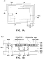
- FIG. 1A shows a top view of a display device according to an embodiment of the present disclosure
- FIG. 1B to FIG. 1D show cross-sectional views along the cross-sectional line 1B-1B' in FIG. 1A according to some embodiments of the present disclosure
- FIG. 1E shows a 3D diagram of a spacer according to an embodiment of the present disclosure
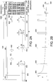
- FIG. 2A shows a partial top view of a display device according to an embodiment of the present disclosure
- FIG. 2B shows a cross-sectional view along the cross-sectional line 2B-2B' in FIG. 2A.
- FIG. 2A is the top view of the region 2A in FIG. 1A .
- the display device 10 As shown in FIGS. 1A-1D and 2A-2B , the display device 10, as well as the display device 10-1, the display device 10-2 and the display deice 10-3, includes a first substrate 100, a color filter 200, a first electrode layer 300, a first alignment layer 400, a second substrate 500 and a display layer 600.
- the first substrate 100 has a display region 110 and a border region 120.
- the color filter 200 is disposed corresponding to the display region 110 of the first substrate 100, the color filter 200 includes a plurality of first pixel regions and a plurality of second pixel regions arranged staggeredly, and the first pixel regions and the second pixel regions are pixel regions with different colors.
- the first pixel regions are such as green pixel regions 200G
- the second pixel regions are such as red pixel regions 200R and/or blue pixel regions 200B
- the color filter 200 includes a plurality of red pixel regions 200R, a plurality of green pixel regions 200G and a plurality of blue pixel regions 200B which are arranged staggeredly and adjacent to one another.
- the color filter 200 may include a plurality of red pixel regions 200R and a plurality of green pixel region 200G arranged staggeredly, or a plurality of green pixel regions 200G and a plurality of blue pixel regions 200B arranged staggeredly, or a plurality of red pixel regions 200R and a plurality of blue pixel regions 200B arranged staggeredly.
- the color filter 200 may include a plurality of red pixel regions 200R, a plurality of green pixel regions 200G, a plurality of blue pixel regions 200B and a plurality of white pixel regions (i.e.
- the color filter 200 may include a plurality of red pixel regions 200R, a plurality of green pixel regions 200G, a plurality of blue pixel regions 200B and a plurality of yellow pixel regions; the present disclosure is not limited thereto.
- the first electrode layer 300 is disposed on the first substrate 100, and the first alignment layer 400 is disposed on the first electrode layer 300.
- the display layer 600 is disposed between the first substrate 100 and the second substrate 200.
- the red pixel regions 200R, the green pixel regions 200G and the blue pixel regions 200B in the display region 110 are arranged repeatedly and sequentially, where one red pixel region 200R, one green pixel region 200G and one blue pixel region 200B form a pixel, and multiple pixels are arranged as a matrix.
- one red pixel region 200R is arranged adjacent to one green pixel region 200G and one blue pixel region 200B
- one green pixel region 200G is arranged adjacent to one red pixel region 200R and one blue pixel region 200B
- one blue pixel region 200B is arranged adjacent to one green pixel region 200G and one red pixel region 200R.
- an interface 100A is located between the display region 110 and the border region 120.
- the two portions of the first alignment layer 400 respectively corresponding to the display region 110 and the border region 120 could have different thicknesses.
- the portion of the first alignment layer 400 corresponding to the display region 110 has a thickness substantially less than that of the portion of the first alignment layer 400 corresponding to the border region 120.
- the first alignment layer 400 corresponding to (located above or below) a first one of the plurality of the first pixel regions counting from the interface 100A towards the display region 110 has a first thickness T1
- the first alignment layer 400 corresponding to (located above or below) the fourth one of the plurality of the first pixel regions counting from the interface 100A towards the display region 110 has a second thickness T2
- the first thickness T1 and the second thickness T2 are in units of micrometers ( ⁇ m)
- the values of the first thickness T1 and the second thickness T2 satisfy the following condition: 0.8 ⁇ T1/T2 ⁇ 1.2.
- the first alignment layer 400 corresponding to (located above or below) the first green pixel region 200G (200G1) of the plurality of the green pixel regions 200B counting from the interface 100A towards the display region 110 has a first thickness T1
- the first alignment layer 400 corresponding to (located above or below) the fourth green pixel region 200G (200G4) of the plurality of the green pixel regions 200G counting from the interface 100A towards the display region 110 has a second thickness T2
- the first thickness T1 and the second thickness T2 are in units of micrometers ( ⁇ m)
- the values of the first thickness T1 and the second thickness T2 satisfy the following condition: 0.8 ⁇ T1/T2 ⁇ 1.2.
- the variance between the thickness of the first alignment layer 400 corresponding to the first green pixel region 200G1 and the thickness of the first alignment layer 400 corresponding to the fourth green pixel region 200G4 counting from the interface 100A towards the display region 110 is greater than 0% and equal to or less than 20%. That is, the first thickness T1 is different from the second thickness T2.
- the distance between the interface 100A and the green pixel region 200G1 of the first pixel is such as about 50 ⁇ m
- the distance between the interface 100A and the green pixel region 200G4 of the fourth pixel is such as about 1000 ⁇ m.
- the variance between the thicknesses of the first alignment layer corresponding to the first pixel region and the fourth pixel region of different colors is also greater than 0% and equal to or less than 20%.
- the variance between the thickness of the first alignment layer 400 corresponding to the first pixel region (e.g. the green pixel region 200G1) of the plurality of the first pixel regions and the thickness of the first alignment layer 400 corresponding to the fourth pixel region (e.g. the green pixel region 200G4)of the plurality of the first pixel regions counting from the interface 100A towards the display region 110 is greater than 0% and equal to or less than 20%, indicating that the thickness of the first alignment layer 400 is provided with excellent uniformity, such that the occurrence of mura can be reduced, and the display quality of the display device can be increased.
- the display layer 600 is such as a liquid crystal layer
- the first electrode layer 300 is such as a transparent electrode layer, for example, an ITO layer or a transparent conductive layer made of other metal oxide conductive materials.
- the first electrode layer 300 is such as a common electrode.
- the display device may further include an sealant 700 and a plurality of spacers 800.
- the sealant 700 is disposed on the border region 120 and surrounds the display region 110 of the first substrate 100.
- the spacers 800 are disposed between the first substrate 100 and the second substrate 500.
- a height H of the spacers 800 is such as greater than or equal to 2 ⁇ m and less than or equal to 5 ⁇ m.
- a spacing between two adjacent of the spacers 800 in the border region 120 is such as greater than or equal to 25 ⁇ m and less than or equal to 500 ⁇ m.
- the spacers 800 have a first width P along an extending direction of the interface 100A between the display region 110 and the border region 120, the spacers 800 have a second width Q along a direction perpendicular to the extending direction of the interface 100A, the first width P and the second width Q are in units of micrometers ( ⁇ m), and the values of the first width P and the second width Q of the spacers 800 in the border region 120 may satisfy the following condition: 0.1 ⁇ Q/P ⁇ 100.
- the process of forming the first alignment layer 400 includes coating an alignment layer liquid material on the first substrate 100 and performing a baking step to form the first alignment layer 400.
- the 3D structures e.g. the spacers
- the process of forming the first alignment layer 400 may cause the liquid material to retain on the surfaces of the 3D structures and induce surface tension phenomenon, which may result in un-uniform thickness distribution of the coating layer of the alignment layer liquid material.
- the ratio of two widths of the spacer 800 is limited within the above range, such that the surface tension phenomenon is reduced, the un-uniform thickness distribution phenomenon of the coating layer of the alignment layer liquid material caused by the 3D structures of the spacers 800 can be improved. Accordingly, the thickness uniformity of the as-formed first alignment layer 400 can be improved, and the display quality can be increased.
- the shape of the spacer 800 as shown in FIG. 2A is a top view shape as viewed from a top view perspective perpendicular to the substrate.
- the border region 120 may have a first zone 121, and the first zone 121 is defined as an area extending from the interface 100A between the display region 110 and the border region 120 towards the sealant 700 by 100 ⁇ m. As shown in FIG. 1A and FIG. 2A , the first zone 121 covers the area extending from the outer periphery (i.e. the interface 100A) of the display region 110 outwards by 100 ⁇ m, and surrounds the display region 110.
- the spacers 800 in the first zone 121 are such as conductive stoppers for preventing the shortcuts of conductive structures located above and below the spacers 800 as well as providing supports.
- the above is an example only, and the spacers 800 in the first zone 121 of the present application are not limited to be conductive stoppers.
- the first width P and the second width Q are in units of micrometers ( ⁇ m), and the values of the first width P and the second width Q of the spacers 800 in the first zone 121 may satisfy the following condition: 0 ⁇ P/Q ⁇ 1.
- the first width P and the second width Q are in units of micrometers ( ⁇ m), and the first width P and the second width Q of the spacers 800 in the first zone 121 may further satisfy the following condition: 0.01 ⁇ P/Q ⁇ 1.
- the process of forming the first alignment layer 400 includes coating an alignment layer liquid material on the first substrate 100, and the liquid material retained on the surfaces of the 3D structures (e.g. the spacers) and the induced surface tension phenomenon may result in un-uniform thickness distribution of the coating layer of the alignment layer liquid material. As shown in FIG.
- the capillarity phenomenon caused by the 3D structures in the first zone 121 may cause an undesired increase of the liquid level of the coating liquid in the first zone 121, leaving an increased amount of the coating liquid retained in the first zone 121, inevitably resulting in a decrease of the amount of the coating liquid in the display region 110 which is adjacent to the first zone 121, such that an undesired decrease of the liquid level of the coating layer of the alignment layer liquid material in the display region 110 occurs.
- the first alignment layer 400 in the border region 120 is facing the uniform thickness issue, but the first alignment layer 400 in the display region 110 is also provided with uniform thickness.
- the shapes of the spacers 800 in the first zone 121 are close to circular forms, as shown in FIG. 2A ; given that liquid surface tension force is inversely proportional to the liquid contact length between liquid and 3D structures, such that the spacers 800 conformed to the above conditions can provide a relatively large supporting area (i.e. the cross-sectional area 800a of the top portion of the spacer 800, as shown in FIG.
- the coating liquid retained in the first zone 121 can be reduced, and the undesired decrease of the coating liquid in the display region 110 can be further reduced, and the predetermined thickness of the coating layer of the alignment layer liquid material in the display region 110 can be maintained. Accordingly, when the first width P and the second width Q of the spacers 800 in the first zone 121 are conformed to the above conditions, the thickness uniformity of the first alignment layer 400 in the display region 110 and the first zone 121 can be both improved, the occurrence of mura can be reduced, and the display quality of the display device can be increased.
- a spacing D1 between two adjacent of the spacers 800 in the first zone 121 is such as greater than or equal to 5 ⁇ m and less than or equal to 90 ⁇ m. Given that the distance between 3D structures is inversely proportional to the strength of capillarity phenomenon, according to the embodiments of the present disclosure, the spacing D1 between two adjacent of the spacers 800 in the first zone 121 is relatively small, the shapes of the spacers 800 are close to circular forms, and thus the capillarity phenomenon occurred on the coating liquid can be diminished, the issues of un-uniform thickness distribution of the coating layer of the alignment layer liquid material can be improved, and the thickness uniformity of the first alignment layer 400 can be increased.
- the border region 120 may further have a second zone 123, and the second zone 123 is defined as an area extending from a location distanced from the interface 100A by 100 ⁇ m towards the sealant 700 and stopped at a location distanced from the interface 100A by 800 ⁇ m.
- the second zone 123 covers the area extending from the outer periphery of the first zone 121 towards the sealant 700 by 700 ⁇ m, and surrounds the display region 110 and the first zone 121.
- the spacers 800 in the second zone 123 are such as gap supports for providing supports.
- the above is an example only, and the spacers 800 in the second zone 123 of the present application are not limited to be gap supports.
- the spacers 800 in the second zone 123 are distanced from the interface 100A by a distance B (only one label of the distance B between one spacer 800 and the interface 100A is shown in drawings for exemplification), the first width P, the second width Q and the first distance B are in units of micrometers ( ⁇ m), and the values (with no units) of the first width P, the second width Q and the first distance B are conformed to the following condition: P/Q ⁇ (B-70)/30, 100 ⁇ B ⁇ 800.
- the effects of the present disclosure cannot be achieved, and undesired influences of causing the thickness of the first alignment layer 400 to be un-uniform may occur.
- a spacing D2 between two adjacent of the spacers 800 in the second zone 123 is such as greater than or equal to 5 ⁇ m and less than or equal to 600 ⁇ m.
- the border region 120 may further include a third zone 125, and the third zone 125 is defined as an area extending from an outer periphery of the second zone 123 to the sealant 700.
- the third zone 125 covers the area extending from the outer periphery of the second zone towards and stopped at the sealant 700, and surrounds the display region 110, the first zone 121 and the second zone 123.
- the spacers 800 in the third zone 125 are such as liquid barriers for preventing the coating liquid of the alignment layer to overflow towards regions outside the sealant 700.
- the spacers 800 in the third zone 125 are not limited to be liquid barriers.
- the first width P and the second width Q of the spacers 800 as well as the spacing between two adjacent of the spacers 800 in the third zone 125 may not be necessarily conformed to the conditions referring to the first zone 121 and/or the second zone 123 as aforementioned.
- first substrate 100 The arrangements of the first substrate 100, the color filter 200, the first electrode layer 300, the first alignment layer 400, the second substrate 500, the display layer 600, the sealant 700 and the spacers 800 as described in previous embodiments of the present disclosure may be applied in display devices of additional various embodiments.
- the display device 10-1 may further include a pixel electrode 910 disposed on the second substrate 500.
- the display device 10-1 may further include a second alignment layer 920 disposed on the pixel electrode 910.
- the first substrate 100 is such as a glass substrate, a plastic substrate or a substrate of other kinds;
- the second substrate 500 is such as a TFT substrate;
- the spacers 800 are disposed on the first substrate 100 and the color filter 200;
- the display device 10-1 is such as a VA type liquid crystal display device.
- the display device 10-1 as shown in FIG. 1B may not include a second alignment layer 920 (not shown in drawings), and thus the display device 10-1 without a second alignment layer 920 is such as an IPS type liquid crystal display device or a FFS type liquid crystal display device.
- the first substrate 100 is such as a glass substrate
- the second substrate 500 is such as a TFT substrate
- the spacers 800 are disposed on the second substrate (e.g. TFT substrate)
- the display device 10-2 is such as a VA type liquid crystal display device.
- the display device 10-2 without a second alignment layer 920 is such as an IPS type liquid crystal display device or a FFS type liquid crystal display device.
- the first substrate 100 is such as a glass substrate
- the second substrate 500 is such as a TFT substrate
- the color filter 200 and the spacers 800 are all disposed on the second substrate (e.g. TFT substrate)
- the display device 10-3 is such as a VA type liquid crystal display device.
- the display device 10-3 without a second alignment layer 920 is such as an IPS type liquid crystal display device or a FFS type liquid crystal display device.
- the first electrode layer 300 may be presented in forms as shown in the drawings where the electrode patterns are in forms of multiple regions which are designed according to the masks; the first electrode layer 300 may as well be presented as a whole plane of electrode layer which extends to the edge of the encapsulation layer (not shown in drawings) without applying any masks.
Landscapes
- Physics & Mathematics (AREA)
- Nonlinear Science (AREA)
- Mathematical Physics (AREA)
- Chemical & Material Sciences (AREA)
- Crystallography & Structural Chemistry (AREA)
- General Physics & Mathematics (AREA)
- Optics & Photonics (AREA)
- Spectroscopy & Molecular Physics (AREA)
- Geometry (AREA)
- Liquid Crystal (AREA)
- Devices For Indicating Variable Information By Combining Individual Elements (AREA)
Abstract
Description
- The present disclosure relates to a display device, and particularly to a display device including an alignment layer.
- The alignment layers in liquid crystal displays are usually manufactured by wet coating processes, such as a flexographic printing process or an ink-jet printing process. In the flexographic printing process, the coating solution is printed on the to-be-coated surfaces by roller coating, and in the ink-jet printing process, the coating solution is sprayed onto the to-be-coated surfaces through spraying holes.
- However, when the quality of the alignment layers is unsatisfactory, it may result in having undesired influences on the display qualities of the displays. Therefore, these are needs to provide alignment layers with excellent qualities to solve the problems that the conventional technique is facing.
- The present disclosure relates to a display device. In the embodiment, in the display device, the variance between the thickness of the first alignment layer corresponding to a first one of the first pixel regions and the thickness of the first alignment layer corresponding to the fourth one of the first pixel regions counting from the interface towards the display region between the display region and the border region is greater than 0% and equal to or less than 20%, indicating that the thickness of the first alignment layer is provided with excellent uniformity, such that the occurrence of mura can be reduced, and the display quality of the display device can be increased.
- According to an embodiment of the present disclosure, a display device is provided. The display device includes a first substrate, a color filter, a first electrode layer, a first alignment layer, a second substrate and a display layer. The first substrate has a display region and a border region, and an interface is between the display region and the border region. The color filter is disposed corresponding to the display region of the first substrate. The color filter includes a plurality of first pixel regions and a plurality of second pixel regions arranged staggeredly, and the first pixel regions and the second pixel regions are pixel regions with different colors. The first electrode layer is disposed on the first substrate, and the first alignment layer is disposed on the first electrode layer. The first alignment layer corresponding to a first one of the plurality of the first pixel regions counting from the interface towards the display region has a first thickness T1, the first alignment layer corresponding to a fourth one of the plurality of the first pixel regions counting from the interface towards the display region has a second thickness T2. The units of the first thickness T1 and the second thickness T2 are micrometers (µm), and the first thickness T1 and the second thickness T2 are conformed to the following condition: 0.8≤T1/T2≤1.2. The display layer is disposed between the first substrate and the second substrate.
- The following description is made with reference to the accompanying drawings and embodiments.
-
-
FIG. 1A shows a top view of a display device according to an embodiment of the present disclosure; -
FIG. 1B to FIG. 1D show cross-sectional views along thecross-sectional line 1B-1B' inFIG. 1A according to some embodiments of the present disclosure; -
FIG. 1E shows a 3D diagram of a spacer according to an embodiment of the present disclosure; -
FIG. 2A shows a partial top view of a display device according to an embodiment of the present disclosure; and -
FIG. 2B shows a cross-sectional view along thecross-sectional line 2B-2B' inFIG. 2A . - The following description of the embodiments of the present disclosure is made with reference to the accompanying drawings. The embodiments are for exemplification and not for limiting the scope. In the embodiments, the elements sharing similar or the same labels in the drawings are similar or the same elements. The present disclosure can be realized by applying various features, methods and parameters. The detailed structures disclosed in the embodiments are for exemplification only, not for limiting the scope of protection of the disclosure. One of ordinary skills in the art may modify or change the structures according to actual needs. In addition, it is to be noted that the accompanying drawings are simplified with some secondary elements omitted for clearly describing the disclosure.
-
FIG. 1A shows a top view of a display device according to an embodiment of the present disclosure,FIG. 1B to FIG. 1D show cross-sectional views along thecross-sectional line 1B-1B' inFIG. 1A according to some embodiments of the present disclosure,FIG. 1E shows a 3D diagram of a spacer according to an embodiment of the present disclosure,FIG. 2A shows a partial top view of a display device according to an embodiment of the present disclosure, andFIG. 2B shows a cross-sectional view along thecross-sectional line 2B-2B' inFIG. 2A. FIG. 2A is the top view of theregion 2A inFIG. 1A . It is to be noted that some elements are omitted for clearly describing the present disclosure. It is also important to point out that some elements in drawings may not be necessarily drawn to scale; thus, the specification and the drawings are to be regarded as an illustrative sense rather than a restrictive sense. - As shown in
FIGS. 1A-1D and2A-2B , thedisplay device 10, as well as the display device 10-1, the display device 10-2 and the display deice 10-3, includes afirst substrate 100, acolor filter 200, afirst electrode layer 300, afirst alignment layer 400, asecond substrate 500 and adisplay layer 600. Thefirst substrate 100 has adisplay region 110 and aborder region 120. As viewed from the top view perspective, thecolor filter 200 is disposed corresponding to thedisplay region 110 of thefirst substrate 100, thecolor filter 200 includes a plurality of first pixel regions and a plurality of second pixel regions arranged staggeredly, and the first pixel regions and the second pixel regions are pixel regions with different colors. In some embodiments, the first pixel regions are such asgreen pixel regions 200G, and the second pixel regions are such asred pixel regions 200R and/orblue pixel regions 200B. In the present embodiment thecolor filter 200 includes a plurality ofred pixel regions 200R, a plurality ofgreen pixel regions 200G and a plurality ofblue pixel regions 200B which are arranged staggeredly and adjacent to one another. In some other embodiments, thecolor filter 200 may include a plurality ofred pixel regions 200R and a plurality ofgreen pixel region 200G arranged staggeredly, or a plurality ofgreen pixel regions 200G and a plurality ofblue pixel regions 200B arranged staggeredly, or a plurality ofred pixel regions 200R and a plurality ofblue pixel regions 200B arranged staggeredly. In some further embodiments, thecolor filter 200 may include a plurality ofred pixel regions 200R, a plurality ofgreen pixel regions 200G, a plurality ofblue pixel regions 200B and a plurality of white pixel regions (i.e. transparent pixel regions) arranged staggeredly; or, thecolor filter 200 may include a plurality ofred pixel regions 200R, a plurality ofgreen pixel regions 200G, a plurality ofblue pixel regions 200B and a plurality of yellow pixel regions; the present disclosure is not limited thereto. Thefirst electrode layer 300 is disposed on thefirst substrate 100, and thefirst alignment layer 400 is disposed on thefirst electrode layer 300. Thedisplay layer 600 is disposed between thefirst substrate 100 and thesecond substrate 200. - In the present embodiment, as shown in
FIG. 2A , thered pixel regions 200R, thegreen pixel regions 200G and theblue pixel regions 200B in thedisplay region 110 are arranged repeatedly and sequentially, where onered pixel region 200R, onegreen pixel region 200G and oneblue pixel region 200B form a pixel, and multiple pixels are arranged as a matrix. In thedisplay region 110, i.e. non-border region, onered pixel region 200R is arranged adjacent to onegreen pixel region 200G and oneblue pixel region 200B, onegreen pixel region 200G is arranged adjacent to onered pixel region 200R and oneblue pixel region 200B, and oneblue pixel region 200B is arranged adjacent to onegreen pixel region 200G and onered pixel region 200R. - According to the embodiments of the present disclosure, as shown in
FIG. 2A , aninterface 100A is located between thedisplay region 110 and theborder region 120. In some embodiments, the two portions of thefirst alignment layer 400 respectively corresponding to thedisplay region 110 and theborder region 120 could have different thicknesses. For example, in the present embodiment, the portion of thefirst alignment layer 400 corresponding to thedisplay region 110 has a thickness substantially less than that of the portion of thefirst alignment layer 400 corresponding to theborder region 120. Thefirst alignment layer 400 corresponding to (located above or below) a first one of the plurality of the first pixel regions counting from theinterface 100A towards thedisplay region 110 has a first thickness T1, thefirst alignment layer 400 corresponding to (located above or below) the fourth one of the plurality of the first pixel regions counting from theinterface 100A towards thedisplay region 110 has a second thickness T2, the first thickness T1 and the second thickness T2 are in units of micrometers (µm), and the values of the first thickness T1 and the second thickness T2 satisfy the following condition: 0.8≤T1/T2≤1.2. For example, in the present embodiment, as shown inFIG. 2A , Thefirst alignment layer 400 corresponding to (located above or below) the firstgreen pixel region 200G (200G1) of the plurality of thegreen pixel regions 200B counting from theinterface 100A towards thedisplay region 110 has a first thickness T1, thefirst alignment layer 400 corresponding to (located above or below) the fourthgreen pixel region 200G (200G4) of the plurality of thegreen pixel regions 200G counting from theinterface 100A towards thedisplay region 110 has a second thickness T2, the first thickness T1 and the second thickness T2 are in units of micrometers (µm), and the values of the first thickness T1 and the second thickness T2 satisfy the following condition: 0.8≤T1/T2≤1.2. In other words, the variance between the thickness of thefirst alignment layer 400 corresponding to the first green pixel region 200G1 and the thickness of thefirst alignment layer 400 corresponding to the fourth green pixel region 200G4 counting from theinterface 100A towards thedisplay region 110 is greater than 0% and equal to or less than 20%. That is, the first thickness T1 is different from the second thickness T2. In some embodiments, the distance between theinterface 100A and the green pixel region 200G1 of the first pixel is such as about 50µm, and the distance between theinterface 100A and the green pixel region 200G4 of the fourth pixel is such as about 1000µm. In other embodiments, the variance between the thicknesses of the first alignment layer corresponding to the first pixel region and the fourth pixel region of different colors is also greater than 0% and equal to or less than 20%. - According to the embodiments of the present disclosure, the variance between the thickness of the
first alignment layer 400 corresponding to the first pixel region (e.g. the green pixel region 200G1) of the plurality of the first pixel regions and the thickness of thefirst alignment layer 400 corresponding to the fourth pixel region (e.g. the green pixel region 200G4)of the plurality of the first pixel regions counting from theinterface 100A towards thedisplay region 110 is greater than 0% and equal to or less than 20%, indicating that the thickness of thefirst alignment layer 400 is provided with excellent uniformity, such that the occurrence of mura can be reduced, and the display quality of the display device can be increased. - In some embodiments, as shown in
FIGS. 1A-1D , thedisplay layer 600 is such as a liquid crystal layer, and thefirst electrode layer 300 is such as a transparent electrode layer, for example, an ITO layer or a transparent conductive layer made of other metal oxide conductive materials. In some embodiments, thefirst electrode layer 300 is such as a common electrode. - In the embodiments, as shown in
FIGS. 1A-1D , the display device may further include ansealant 700 and a plurality ofspacers 800. Thesealant 700 is disposed on theborder region 120 and surrounds thedisplay region 110 of thefirst substrate 100. Thespacers 800 are disposed between thefirst substrate 100 and thesecond substrate 500. - In some embodiments, a height H of the
spacers 800 is such as greater than or equal to 2µm and less than or equal to 5µm. - In some embodiments, a spacing between two adjacent of the
spacers 800 in theborder region 120 is such as greater than or equal to 25µm and less than or equal to 500µm. - In some embodiments, also referring to
FIG. 2A , thespacers 800 have a first width P along an extending direction of theinterface 100A between thedisplay region 110 and theborder region 120, thespacers 800 have a second width Q along a direction perpendicular to the extending direction of theinterface 100A, the first width P and the second width Q are in units of micrometers (µm), and the values of the first width P and the second width Q of thespacers 800 in theborder region 120 may satisfy the following condition: 0.1≤Q/P≤100. - In the embodiments, the process of forming the
first alignment layer 400 includes coating an alignment layer liquid material on thefirst substrate 100 and performing a baking step to form thefirst alignment layer 400. In the process of forming thefirst alignment layer 400, the 3D structures (e.g. the spacers) on thefirst substrate 100 may cause the liquid material to retain on the surfaces of the 3D structures and induce surface tension phenomenon, which may result in un-uniform thickness distribution of the coating layer of the alignment layer liquid material. According to the embodiments of the present disclosure, when the first width P and the second width Q of thespacers 800 satisfy the above condition of 0.1≤Q/P≤100 and the spacing between two adjacent of thespacers 800 is greater than or equal to 25µm and less than or equal to 500µm, the ratio of two widths of thespacer 800 is limited within the above range, such that the surface tension phenomenon is reduced, the un-uniform thickness distribution phenomenon of the coating layer of the alignment layer liquid material caused by the 3D structures of thespacers 800 can be improved. Accordingly, the thickness uniformity of the as-formedfirst alignment layer 400 can be improved, and the display quality can be increased. The shape of thespacer 800 as shown inFIG. 2A is a top view shape as viewed from a top view perspective perpendicular to the substrate. - In one embodiment, as shown in
FIG. 1A andFIG. 2A , theborder region 120 may have afirst zone 121, and thefirst zone 121 is defined as an area extending from theinterface 100A between thedisplay region 110 and theborder region 120 towards thesealant 700 by 100µm. As shown inFIG. 1A andFIG. 2A , thefirst zone 121 covers the area extending from the outer periphery (i.e. theinterface 100A) of thedisplay region 110 outwards by 100µm, and surrounds thedisplay region 110. - In the embodiments, the
spacers 800 in thefirst zone 121 are such as conductive stoppers for preventing the shortcuts of conductive structures located above and below thespacers 800 as well as providing supports. However, the above is an example only, and thespacers 800 in thefirst zone 121 of the present application are not limited to be conductive stoppers. - In the embodiments, as shown in
FIG. 2A , the first width P and the second width Q are in units of micrometers (µm), and the values of the first width P and the second width Q of thespacers 800 in thefirst zone 121 may satisfy the following condition: 0<P/Q≤1. In some embodiments, the first width P and the second width Q are in units of micrometers (µm), and the first width P and the second width Q of thespacers 800 in thefirst zone 121 may further satisfy the following condition: 0.01≤P/Q≤1. - As previously described, the process of forming the
first alignment layer 400 includes coating an alignment layer liquid material on thefirst substrate 100, and the liquid material retained on the surfaces of the 3D structures (e.g. the spacers) and the induced surface tension phenomenon may result in un-uniform thickness distribution of the coating layer of the alignment layer liquid material. As shown inFIG. 2A , since thefirst zone 121 is the most adjacent zone to thedisplay region 110, when the applied amount of the coating liquid is fixed, the capillarity phenomenon caused by the 3D structures in thefirst zone 121 may cause an undesired increase of the liquid level of the coating liquid in thefirst zone 121, leaving an increased amount of the coating liquid retained in thefirst zone 121, inevitably resulting in a decrease of the amount of the coating liquid in thedisplay region 110 which is adjacent to thefirst zone 121, such that an undesired decrease of the liquid level of the coating layer of the alignment layer liquid material in thedisplay region 110 occurs. As such, not only thefirst alignment layer 400 in theborder region 120 is facing the uniform thickness issue, but thefirst alignment layer 400 in thedisplay region 110 is also provided with uniform thickness. - In contrast, according to the embodiments of the present disclosure, when the values of the first width P and the second width P of the
spacers 800 in thefirst zone 121 are conformed to the condition of 0<P/Q≤1, or even are further conformed to the condition of 0.01≤P/Q≤1, the shapes of thespacers 800 in thefirst zone 121 are close to circular forms, as shown inFIG. 2A ; given that liquid surface tension force is inversely proportional to the liquid contact length between liquid and 3D structures, such that thespacers 800 conformed to the above conditions can provide a relatively large supporting area (i.e. thecross-sectional area 800a of the top portion of thespacer 800, as shown inFIG. 1E ) while the relatively small liquid contact length can diminish the capillarity phenomenon occurred on the coating liquid and improve the issues of un-uniform thickness distribution of the coating layer of the alignment layer liquid material. As such, the coating liquid retained in thefirst zone 121 can be reduced, and the undesired decrease of the coating liquid in thedisplay region 110 can be further reduced, and the predetermined thickness of the coating layer of the alignment layer liquid material in thedisplay region 110 can be maintained. Accordingly, when the first width P and the second width Q of thespacers 800 in thefirst zone 121 are conformed to the above conditions, the thickness uniformity of thefirst alignment layer 400 in thedisplay region 110 and thefirst zone 121 can be both improved, the occurrence of mura can be reduced, and the display quality of the display device can be increased. - In the embodiments, a spacing D1 between two adjacent of the
spacers 800 in thefirst zone 121 is such as greater than or equal to 5µm and less than or equal to 90µm. Given that the distance between 3D structures is inversely proportional to the strength of capillarity phenomenon, according to the embodiments of the present disclosure, the spacing D1 between two adjacent of thespacers 800 in thefirst zone 121 is relatively small, the shapes of thespacers 800 are close to circular forms, and thus the capillarity phenomenon occurred on the coating liquid can be diminished, the issues of un-uniform thickness distribution of the coating layer of the alignment layer liquid material can be improved, and the thickness uniformity of thefirst alignment layer 400 can be increased. - In one embodiment, as shown in
FIG. 1A and2A , theborder region 120 may further have asecond zone 123, and thesecond zone 123 is defined as an area extending from a location distanced from theinterface 100A by 100µm towards thesealant 700 and stopped at a location distanced from theinterface 100A by 800µm. In other words, thesecond zone 123 covers the area extending from the outer periphery of thefirst zone 121 towards thesealant 700 by 700µm, and surrounds thedisplay region 110 and thefirst zone 121. - In the embodiments, the
spacers 800 in thesecond zone 123 are such as gap supports for providing supports. However, the above is an example only, and thespacers 800 in thesecond zone 123 of the present application are not limited to be gap supports. - In the embodiments, as shown in
FIG. 2A , thespacers 800 in thesecond zone 123 are distanced from theinterface 100A by a distance B (only one label of the distance B between onespacer 800 and theinterface 100A is shown in drawings for exemplification), the first width P, the second width Q and the first distance B are in units of micrometers (µm), and the values (with no units) of the first width P, the second width Q and the first distance B are conformed to the following condition: P/Q≤(B-70)/30, 100<B≤800. - For example, when the first width P and the second width Q of the
spacers 800 are 100µm and 6µm respectively, P/Q=16.67. When thespacers 800 are disposed in thesecond zone 123 at a location distanced from theinterface 100A by 161µm, thereby (B-70)/30=(161-70)/30=3, and 3 is not greater than or equal to 16.67. Thus, according to the embodiments of the present disclosure, when thespacers 800 are disposed at a location distanced from theinterface 100A by the distance B of 161 µm, the effects of the present disclosure cannot be achieved, and undesired influences of causing the thickness of thefirst alignment layer 400 to be un-uniform may occur. For example, when thespacers 800 are disposed in thesecond zone 123 at a location distanced from theinterface 100A by 600µm, thereby (B-70)/30=(600-70)/30=17.7, and 17.7 is greater than 16.67. Thus, according to the embodiments of the present disclosure, when thespacers 800 are disposed at a location distanced from theinterface 100A by the distance B of 600µm, the supporting effects can be achieved, and at the meantime the thickness uniformity of thefirst alignment layer 400 can be maintained. In other words, from the above two examples, it is apparent that the condition of P/Q≤(B-70)/30 is crucial in terms of providing the principles for designing the arrangement relationship between the shapes (P/Q) and the arranged positions (distance B) of thespacers 800; when the above condition is satisfied, the effects of thespacers 800 providing supports as well as thefirst alignment layer 400 having uniform thickness can be both achieved. - In the embodiments, a spacing D2 between two adjacent of the
spacers 800 in thesecond zone 123 is such as greater than or equal to 5µm and less than or equal to 600µm. - In one embodiment, as shown in
FIG. 1A , theborder region 120 may further include athird zone 125, and thethird zone 125 is defined as an area extending from an outer periphery of thesecond zone 123 to thesealant 700. In other words, thethird zone 125 covers the area extending from the outer periphery of the second zone towards and stopped at thesealant 700, and surrounds thedisplay region 110, thefirst zone 121 and thesecond zone 123. - In the embodiments, the
spacers 800 in thethird zone 125 are such as liquid barriers for preventing the coating liquid of the alignment layer to overflow towards regions outside thesealant 700. However, the above is an example only, and thespacers 800 in thethird zone 125 are not limited to be liquid barriers. In addition, the first width P and the second width Q of thespacers 800 as well as the spacing between two adjacent of thespacers 800 in thethird zone 125 may not be necessarily conformed to the conditions referring to thefirst zone 121 and/or thesecond zone 123 as aforementioned. - The arrangements of the
first substrate 100, thecolor filter 200, thefirst electrode layer 300, thefirst alignment layer 400, thesecond substrate 500, thedisplay layer 600, thesealant 700 and thespacers 800 as described in previous embodiments of the present disclosure may be applied in display devices of additional various embodiments. - In one embodiment, as shown in
FIG. 1B , the display device 10-1 may further include apixel electrode 910 disposed on thesecond substrate 500. The display device 10-1 may further include asecond alignment layer 920 disposed on thepixel electrode 910. In the embodiment as shown inFIG. 1B , thefirst substrate 100 is such as a glass substrate, a plastic substrate or a substrate of other kinds; thesecond substrate 500 is such as a TFT substrate; thespacers 800 are disposed on thefirst substrate 100 and thecolor filter 200; the display device 10-1 is such as a VA type liquid crystal display device. - In an alternative embodiment, the display device 10-1 as shown in
FIG. 1B may not include a second alignment layer 920 (not shown in drawings), and thus the display device 10-1 without asecond alignment layer 920 is such as an IPS type liquid crystal display device or a FFS type liquid crystal display device. - In one embodiment, as shown in
FIG. 1C , in the display device 10-2, thefirst substrate 100 is such as a glass substrate, thesecond substrate 500 is such as a TFT substrate, thespacers 800 are disposed on the second substrate (e.g. TFT substrate), and the display device 10-2 is such as a VA type liquid crystal display device. Likewise, the display device 10-2 without asecond alignment layer 920 is such as an IPS type liquid crystal display device or a FFS type liquid crystal display device. - In one embodiment, as shown in
FIG. 1D , in the display device 10-3, thefirst substrate 100 is such as a glass substrate, thesecond substrate 500 is such as a TFT substrate, thecolor filter 200 and thespacers 800 are all disposed on the second substrate (e.g. TFT substrate), and the display device 10-3 is such as a VA type liquid crystal display device. Likewise, the display device 10-3 without asecond alignment layer 920 is such as an IPS type liquid crystal display device or a FFS type liquid crystal display device. - In the various embodiments as shown in
FIGS. 1B-1D , thefirst electrode layer 300 may be presented in forms as shown in the drawings where the electrode patterns are in forms of multiple regions which are designed according to the masks; thefirst electrode layer 300 may as well be presented as a whole plane of electrode layer which extends to the edge of the encapsulation layer (not shown in drawings) without applying any masks. - While the disclosure has been described by way of example and in terms of the exemplary embodiment(s), it is to be understood that the disclosure is not limited thereto. On the contrary, it is intended to cover various modifications and similar arrangements and procedures, and the scope of the appended claims therefore should be accorded the broadest interpretation so as to encompass all such modifications and similar arrangements and procedures.
Claims (15)
- A display device, characterized in that the display device comprises:a first substrate (100) having a display region (110) and a border region (120), wherein an interface (100A) is between the display region (110) and the border region (120);a color filter (200) disposed corresponding to the display region, wherein the color filter (200) comprises a plurality of first pixel regions and a plurality of second pixel regions arranged staggeredly, and the plurality of first pixel regions have a color different from that of the second pixel regions;a first electrode layer (300) disposed on the first substrate;a first alignment layer (400) disposed on the first electrode layer, wherein the first alignment layer corresponding to a first one of the plurality of first pixel regions counting from the interface towards the display region has a first thickness T1, the first alignment layer corresponding to a fourth one of the plurality of first pixel regions counting from the interface towards the display region has a second thickness T2, units of the first thickness T1 and the second thickness T2 are micrometers (µm), and the first thickness T1 and the second thickness T2 are conformed to the following condition: 0.8≤T1/T2≤1.2;a second substrate (500), anda display layer (600) disposed between the first substrate and the second substrate.
- The display device according to claim 1, further comprising:a sealant (700) disposed on the border region and surrounding the display region; anda plurality of spacers (800) disposed between the first substrate and the second substrate.
- The display device according to claim 2, wherein the border region has a first zone (121) defined as covering an area extending from the interface towards the sealant by 100µm, one of the plurality of spacers located in the first zone has a first width P along an extending direction of the interface, the one of spacers located in the first zone has a second width Q along a direction perpendicular to the extending direction of the interface, units of the first width P and the second width Q are micrometers (µm), and the first width P and the second width Q of the one of the plurality of spacers located in the first zone are conformed to the following condition: 0<P/Q≤1.
- The display device according to claim 3, wherein the first width P and the second width Q of the one of the plurality of spacers located in the first zone (121) are conformed to the following condition: 0.01≤P/Q≤1.
- The display device according to claim 3, wherein a first spacing (D1) between two adjacent of the plurality of spacers located in the first zone (121) is greater than or equal to 5µm and less than or equal to 90µm.
- The display device according to claim 3, wherein the plurality of spacers located in the first zone (121) are conductive stoppers.
- The display device according to claim 2, wherein the border region has a second zone (123) defined as an area extending from a location distanced from the interface by 100µm towards the sealant and stopping at a location distanced from the interface by 800µm, one of the plurality of spacers located in the second zone has a first width P along an extending direction of the interface, the one of the plurality of spacers located in the second zone has a second width Q along a direction perpendicular to the extending direction of the interface, the one of the plurality of spacers located in the second zone are distanced from the interface by a first distance B, units of the first width P, the second width Q and the first distance B are micrometers (µm), and the first width P, the second width Q and the first distance B are conformed to the following condition: P/Q≤(B-70)/30, 100<B≤800.
- The display device according to claim 7, wherein a second spacing (D2) between two adjacent of the plurality of spacers located in the second zone (123) is greater than or equal to 5µm and smaller than or equal to 600µm.
- The display device according to claim 7, wherein a size of one of the plurality of spacers located in a first zone (121) that is defined as an area extending from the interface towards the sealant by 100µm is smaller than a size of one of the plurality of spacers located in the second zone.
- The display device according to claim 7, characterized in that the border region further has a third zone (125) defined as an area extending from an outer periphery of the second zone to the sealant.
- The display device according to claim 2, wherein a height (H) of one of the spacers is greater than or equal to 2µm and less than or equal to 5µm.
- The display device according to claim 2, wherein a third spacing (D3) between two adjacent of the plurality of spacers in the border region is greater than or equal to 25µm and less than or equal to 500µm.
- The display device according to claim 2, wherein one of the plurality of spacers has a first width P along an extending direction of the interface, the one of the plurality of spacers has a second width Q along a direction perpendicular to the extending direction of the interface, units of the first width P and the second width Q are micrometers (µm), and the first width P and the second width Q of the one of the plurality of spacers in the border region are conformed to the following condition: 0.1≤Q/P≤100.
- The display device according to claim 1, further comprising:a pixel electrode (910) disposed on the second substrate; anda second alignment layer (920) disposed on the pixel electrode.
- The display device according to claim 1, wherein the first thickness is different from the second thickness.
Applications Claiming Priority (1)
| Application Number | Priority Date | Filing Date | Title |
|---|---|---|---|
| TW106119924A TW201905551A (en) | 2017-06-15 | 2017-06-15 | Display device |
Publications (2)
| Publication Number | Publication Date |
|---|---|
| EP3415983A1 true EP3415983A1 (en) | 2018-12-19 |
| EP3415983B1 EP3415983B1 (en) | 2020-09-16 |
Family
ID=62563073
Family Applications (1)
| Application Number | Title | Priority Date | Filing Date |
|---|---|---|---|
| EP18176477.0A Active EP3415983B1 (en) | 2017-06-15 | 2018-06-07 | Display device |
Country Status (3)
| Country | Link |
|---|---|
| US (1) | US10809572B2 (en) |
| EP (1) | EP3415983B1 (en) |
| TW (1) | TW201905551A (en) |
Cited By (1)
| Publication number | Priority date | Publication date | Assignee | Title |
|---|---|---|---|---|
| CN113075811A (en) * | 2020-01-06 | 2021-07-06 | 群创光电股份有限公司 | Electronic device |
Families Citing this family (3)
| Publication number | Priority date | Publication date | Assignee | Title |
|---|---|---|---|---|
| KR20190124845A (en) * | 2018-04-26 | 2019-11-06 | 삼성디스플레이 주식회사 | Display device and method for manufacturing display device |
| CN110174803A (en) * | 2019-05-10 | 2019-08-27 | 深圳市华星光电技术有限公司 | Array substrate and preparation method thereof |
| CN113934044A (en) * | 2020-06-29 | 2022-01-14 | 京东方科技集团股份有限公司 | Display panel and display device |
Citations (3)
| Publication number | Priority date | Publication date | Assignee | Title |
|---|---|---|---|---|
| US20090009697A1 (en) * | 2004-08-04 | 2009-01-08 | Sharp Kabushiki Kaisha | Color filter substrate and liquid crystal display panel equipped with same |
| US20120194494A1 (en) * | 2011-01-31 | 2012-08-02 | Samsung Electronics Co., Ltd. | Display panel and method of manufacturing the same |
| US20160124255A1 (en) * | 2013-08-20 | 2016-05-05 | Sharp Kabushiki Kaisha | Display component, display device, and television device |
Family Cites Families (4)
| Publication number | Priority date | Publication date | Assignee | Title |
|---|---|---|---|---|
| TWI286224B (en) | 2006-08-03 | 2007-09-01 | Au Optronics Corp | Color filter substrate and fabricating method thereof |
| JP2014211592A (en) | 2013-04-22 | 2014-11-13 | セイコーエプソン株式会社 | Liquid crystal device, manufacturing method of liquid crystal device, and electronic apparatus |
| US9733509B2 (en) * | 2015-08-06 | 2017-08-15 | Chunghwa Picture Tubes, Ltd. | LCD display panel and color filter substrate |
| TWI704411B (en) * | 2017-04-25 | 2020-09-11 | 友達光電股份有限公司 | Photo mask, corresponding spacer structure and liquid crystal panel using the same |
-
2017
- 2017-06-15 TW TW106119924A patent/TW201905551A/en unknown
-
2018
- 2018-05-21 US US15/984,513 patent/US10809572B2/en active Active
- 2018-06-07 EP EP18176477.0A patent/EP3415983B1/en active Active
Patent Citations (3)
| Publication number | Priority date | Publication date | Assignee | Title |
|---|---|---|---|---|
| US20090009697A1 (en) * | 2004-08-04 | 2009-01-08 | Sharp Kabushiki Kaisha | Color filter substrate and liquid crystal display panel equipped with same |
| US20120194494A1 (en) * | 2011-01-31 | 2012-08-02 | Samsung Electronics Co., Ltd. | Display panel and method of manufacturing the same |
| US20160124255A1 (en) * | 2013-08-20 | 2016-05-05 | Sharp Kabushiki Kaisha | Display component, display device, and television device |
Cited By (2)
| Publication number | Priority date | Publication date | Assignee | Title |
|---|---|---|---|---|
| CN113075811A (en) * | 2020-01-06 | 2021-07-06 | 群创光电股份有限公司 | Electronic device |
| CN113075811B (en) * | 2020-01-06 | 2023-08-18 | 群创光电股份有限公司 | electronic device |
Also Published As
| Publication number | Publication date |
|---|---|
| US10809572B2 (en) | 2020-10-20 |
| TW201905551A (en) | 2019-02-01 |
| US20180364506A1 (en) | 2018-12-20 |
| EP3415983B1 (en) | 2020-09-16 |
Similar Documents
| Publication | Publication Date | Title |
|---|---|---|
| EP3415983B1 (en) | Display device | |
| CN103676293B (en) | A kind of color membrane substrates and preparation method thereof, display device | |
| US11347111B2 (en) | Method for manufacturing display panel and display panel | |
| KR102001839B1 (en) | Display substrate, mask for manufacturing the same, method of manufacturing the display substrate | |
| CN110850629A (en) | Color film substrate, display panel and display device | |
| US11500249B2 (en) | Counter substrate and display panel | |
| JP2010039187A (en) | Display element | |
| KR20010007429A (en) | Liquid-crystal display panel and method for manufacturing same | |
| WO2016145773A1 (en) | Color film substrate, touch display screen and method for manufacturing color film substrate | |
| CN108227273B (en) | Display panel, color filter substrate and manufacturing method of color filter substrate | |
| US20210080780A1 (en) | Liquid crystal display panel | |
| KR100741903B1 (en) | Liquid dropping LCD panel and manufacturing method thereof | |
| US20200081301A1 (en) | Array substrate and display panel | |
| US10317738B2 (en) | Array substrate and a display panel | |
| WO2020052097A1 (en) | Array substrate and display panel | |
| CN108153033A (en) | Optical filter and its manufacturing method, mask plate and liquid crystal display device | |
| US10802314B2 (en) | Liquid crystal display device | |
| JP2017122790A (en) | Liquid crystal display device | |
| CN202494843U (en) | Color film substrate, liquid crystal panel comprising color membrane substrate, and display device | |
| WO2020206779A1 (en) | Color film substrate and display panel | |
| CN109143656B (en) | Display device | |
| CN110109294A (en) | A kind of liquid crystal display panel, production method and display device | |
| CN105068307A (en) | Substrate with colored film, display device and making method | |
| CN101937149A (en) | Panel for liquid crystal display device | |
| TWI400524B (en) | Liquid crystal display process panel and method for forming alignment film |
Legal Events
| Date | Code | Title | Description |
|---|---|---|---|
| PUAI | Public reference made under article 153(3) epc to a published international application that has entered the european phase |
Free format text: ORIGINAL CODE: 0009012 |
|
| STAA | Information on the status of an ep patent application or granted ep patent |
Free format text: STATUS: THE APPLICATION HAS BEEN PUBLISHED |
|
| AK | Designated contracting states |
Kind code of ref document: A1 Designated state(s): AL AT BE BG CH CY CZ DE DK EE ES FI FR GB GR HR HU IE IS IT LI LT LU LV MC MK MT NL NO PL PT RO RS SE SI SK SM TR |
|
| AX | Request for extension of the european patent |
Extension state: BA ME |
|
| STAA | Information on the status of an ep patent application or granted ep patent |
Free format text: STATUS: REQUEST FOR EXAMINATION WAS MADE |
|
| 17P | Request for examination filed |
Effective date: 20190617 |
|
| RBV | Designated contracting states (corrected) |
Designated state(s): AL AT BE BG CH CY CZ DE DK EE ES FI FR GB GR HR HU IE IS IT LI LT LU LV MC MK MT NL NO PL PT RO RS SE SI SK SM TR |
|
| GRAP | Despatch of communication of intention to grant a patent |
Free format text: ORIGINAL CODE: EPIDOSNIGR1 |
|
| STAA | Information on the status of an ep patent application or granted ep patent |
Free format text: STATUS: GRANT OF PATENT IS INTENDED |
|
| INTG | Intention to grant announced |
Effective date: 20200316 |
|
| GRAS | Grant fee paid |
Free format text: ORIGINAL CODE: EPIDOSNIGR3 |
|
| GRAJ | Information related to disapproval of communication of intention to grant by the applicant or resumption of examination proceedings by the epo deleted |
Free format text: ORIGINAL CODE: EPIDOSDIGR1 |
|
| GRAL | Information related to payment of fee for publishing/printing deleted |
Free format text: ORIGINAL CODE: EPIDOSDIGR3 |
|
| STAA | Information on the status of an ep patent application or granted ep patent |
Free format text: STATUS: REQUEST FOR EXAMINATION WAS MADE |
|
| GRAR | Information related to intention to grant a patent recorded |
Free format text: ORIGINAL CODE: EPIDOSNIGR71 |
|
| STAA | Information on the status of an ep patent application or granted ep patent |
Free format text: STATUS: GRANT OF PATENT IS INTENDED |
|
| INTC | Intention to grant announced (deleted) | ||
| GRAA | (expected) grant |
Free format text: ORIGINAL CODE: 0009210 |
|
| STAA | Information on the status of an ep patent application or granted ep patent |
Free format text: STATUS: THE PATENT HAS BEEN GRANTED |
|
| INTG | Intention to grant announced |
Effective date: 20200806 |
|
| AK | Designated contracting states |
Kind code of ref document: B1 Designated state(s): AL AT BE BG CH CY CZ DE DK EE ES FI FR GB GR HR HU IE IS IT LI LT LU LV MC MK MT NL NO PL PT RO RS SE SI SK SM TR |
|
| REG | Reference to a national code |
Ref country code: GB Ref legal event code: FG4D |
|
| REG | Reference to a national code |
Ref country code: CH Ref legal event code: EP |
|
| REG | Reference to a national code |
Ref country code: DE Ref legal event code: R096 Ref document number: 602018007821 Country of ref document: DE |
|
| REG | Reference to a national code |
Ref country code: IE Ref legal event code: FG4D |
|
| REG | Reference to a national code |
Ref country code: AT Ref legal event code: REF Ref document number: 1314685 Country of ref document: AT Kind code of ref document: T Effective date: 20201015 |
|
| PG25 | Lapsed in a contracting state [announced via postgrant information from national office to epo] |
Ref country code: FI Free format text: LAPSE BECAUSE OF FAILURE TO SUBMIT A TRANSLATION OF THE DESCRIPTION OR TO PAY THE FEE WITHIN THE PRESCRIBED TIME-LIMIT Effective date: 20200916 Ref country code: SE Free format text: LAPSE BECAUSE OF FAILURE TO SUBMIT A TRANSLATION OF THE DESCRIPTION OR TO PAY THE FEE WITHIN THE PRESCRIBED TIME-LIMIT Effective date: 20200916 Ref country code: HR Free format text: LAPSE BECAUSE OF FAILURE TO SUBMIT A TRANSLATION OF THE DESCRIPTION OR TO PAY THE FEE WITHIN THE PRESCRIBED TIME-LIMIT Effective date: 20200916 Ref country code: NO Free format text: LAPSE BECAUSE OF FAILURE TO SUBMIT A TRANSLATION OF THE DESCRIPTION OR TO PAY THE FEE WITHIN THE PRESCRIBED TIME-LIMIT Effective date: 20201216 Ref country code: GR Free format text: LAPSE BECAUSE OF FAILURE TO SUBMIT A TRANSLATION OF THE DESCRIPTION OR TO PAY THE FEE WITHIN THE PRESCRIBED TIME-LIMIT Effective date: 20201217 Ref country code: BG Free format text: LAPSE BECAUSE OF FAILURE TO SUBMIT A TRANSLATION OF THE DESCRIPTION OR TO PAY THE FEE WITHIN THE PRESCRIBED TIME-LIMIT Effective date: 20201216 |
|
| REG | Reference to a national code |
Ref country code: AT Ref legal event code: MK05 Ref document number: 1314685 Country of ref document: AT Kind code of ref document: T Effective date: 20200916 |
|
| REG | Reference to a national code |
Ref country code: NL Ref legal event code: MP Effective date: 20200916 |
|
| PG25 | Lapsed in a contracting state [announced via postgrant information from national office to epo] |
Ref country code: LV Free format text: LAPSE BECAUSE OF FAILURE TO SUBMIT A TRANSLATION OF THE DESCRIPTION OR TO PAY THE FEE WITHIN THE PRESCRIBED TIME-LIMIT Effective date: 20200916 Ref country code: RS Free format text: LAPSE BECAUSE OF FAILURE TO SUBMIT A TRANSLATION OF THE DESCRIPTION OR TO PAY THE FEE WITHIN THE PRESCRIBED TIME-LIMIT Effective date: 20200916 |
|
| REG | Reference to a national code |
Ref country code: LT Ref legal event code: MG4D |
|
| PG25 | Lapsed in a contracting state [announced via postgrant information from national office to epo] |
Ref country code: SM Free format text: LAPSE BECAUSE OF FAILURE TO SUBMIT A TRANSLATION OF THE DESCRIPTION OR TO PAY THE FEE WITHIN THE PRESCRIBED TIME-LIMIT Effective date: 20200916 Ref country code: LT Free format text: LAPSE BECAUSE OF FAILURE TO SUBMIT A TRANSLATION OF THE DESCRIPTION OR TO PAY THE FEE WITHIN THE PRESCRIBED TIME-LIMIT Effective date: 20200916 Ref country code: EE Free format text: LAPSE BECAUSE OF FAILURE TO SUBMIT A TRANSLATION OF THE DESCRIPTION OR TO PAY THE FEE WITHIN THE PRESCRIBED TIME-LIMIT Effective date: 20200916 Ref country code: RO Free format text: LAPSE BECAUSE OF FAILURE TO SUBMIT A TRANSLATION OF THE DESCRIPTION OR TO PAY THE FEE WITHIN THE PRESCRIBED TIME-LIMIT Effective date: 20200916 Ref country code: PT Free format text: LAPSE BECAUSE OF FAILURE TO SUBMIT A TRANSLATION OF THE DESCRIPTION OR TO PAY THE FEE WITHIN THE PRESCRIBED TIME-LIMIT Effective date: 20210118 Ref country code: CZ Free format text: LAPSE BECAUSE OF FAILURE TO SUBMIT A TRANSLATION OF THE DESCRIPTION OR TO PAY THE FEE WITHIN THE PRESCRIBED TIME-LIMIT Effective date: 20200916 |
|
| PG25 | Lapsed in a contracting state [announced via postgrant information from national office to epo] |
Ref country code: AL Free format text: LAPSE BECAUSE OF FAILURE TO SUBMIT A TRANSLATION OF THE DESCRIPTION OR TO PAY THE FEE WITHIN THE PRESCRIBED TIME-LIMIT Effective date: 20200916 Ref country code: AT Free format text: LAPSE BECAUSE OF FAILURE TO SUBMIT A TRANSLATION OF THE DESCRIPTION OR TO PAY THE FEE WITHIN THE PRESCRIBED TIME-LIMIT Effective date: 20200916 Ref country code: ES Free format text: LAPSE BECAUSE OF FAILURE TO SUBMIT A TRANSLATION OF THE DESCRIPTION OR TO PAY THE FEE WITHIN THE PRESCRIBED TIME-LIMIT Effective date: 20200916 Ref country code: PL Free format text: LAPSE BECAUSE OF FAILURE TO SUBMIT A TRANSLATION OF THE DESCRIPTION OR TO PAY THE FEE WITHIN THE PRESCRIBED TIME-LIMIT Effective date: 20200916 Ref country code: IS Free format text: LAPSE BECAUSE OF FAILURE TO SUBMIT A TRANSLATION OF THE DESCRIPTION OR TO PAY THE FEE WITHIN THE PRESCRIBED TIME-LIMIT Effective date: 20210116 |
|
| REG | Reference to a national code |
Ref country code: DE Ref legal event code: R097 Ref document number: 602018007821 Country of ref document: DE |
|
| PG25 | Lapsed in a contracting state [announced via postgrant information from national office to epo] |
Ref country code: SK Free format text: LAPSE BECAUSE OF FAILURE TO SUBMIT A TRANSLATION OF THE DESCRIPTION OR TO PAY THE FEE WITHIN THE PRESCRIBED TIME-LIMIT Effective date: 20200916 |
|
| PLBE | No opposition filed within time limit |
Free format text: ORIGINAL CODE: 0009261 |
|
| STAA | Information on the status of an ep patent application or granted ep patent |
Free format text: STATUS: NO OPPOSITION FILED WITHIN TIME LIMIT |
|
| 26N | No opposition filed |
Effective date: 20210617 |
|
| PG25 | Lapsed in a contracting state [announced via postgrant information from national office to epo] |
Ref country code: DK Free format text: LAPSE BECAUSE OF FAILURE TO SUBMIT A TRANSLATION OF THE DESCRIPTION OR TO PAY THE FEE WITHIN THE PRESCRIBED TIME-LIMIT Effective date: 20200916 Ref country code: SI Free format text: LAPSE BECAUSE OF FAILURE TO SUBMIT A TRANSLATION OF THE DESCRIPTION OR TO PAY THE FEE WITHIN THE PRESCRIBED TIME-LIMIT Effective date: 20200916 |
|
| PG25 | Lapsed in a contracting state [announced via postgrant information from national office to epo] |
Ref country code: IT Free format text: LAPSE BECAUSE OF FAILURE TO SUBMIT A TRANSLATION OF THE DESCRIPTION OR TO PAY THE FEE WITHIN THE PRESCRIBED TIME-LIMIT Effective date: 20200916 |
|
| PG25 | Lapsed in a contracting state [announced via postgrant information from national office to epo] |
Ref country code: MC Free format text: LAPSE BECAUSE OF FAILURE TO SUBMIT A TRANSLATION OF THE DESCRIPTION OR TO PAY THE FEE WITHIN THE PRESCRIBED TIME-LIMIT Effective date: 20200916 |
|
| REG | Reference to a national code |
Ref country code: CH Ref legal event code: PL |
|
| REG | Reference to a national code |
Ref country code: BE Ref legal event code: MM Effective date: 20210630 |
|
| PG25 | Lapsed in a contracting state [announced via postgrant information from national office to epo] |
Ref country code: LU Free format text: LAPSE BECAUSE OF NON-PAYMENT OF DUE FEES Effective date: 20210607 |
|
| PG25 | Lapsed in a contracting state [announced via postgrant information from national office to epo] |
Ref country code: LI Free format text: LAPSE BECAUSE OF NON-PAYMENT OF DUE FEES Effective date: 20210630 Ref country code: IE Free format text: LAPSE BECAUSE OF NON-PAYMENT OF DUE FEES Effective date: 20210607 Ref country code: CH Free format text: LAPSE BECAUSE OF NON-PAYMENT OF DUE FEES Effective date: 20210630 |
|
| PG25 | Lapsed in a contracting state [announced via postgrant information from national office to epo] |
Ref country code: BE Free format text: LAPSE BECAUSE OF NON-PAYMENT OF DUE FEES Effective date: 20210630 |
|
| PG25 | Lapsed in a contracting state [announced via postgrant information from national office to epo] |
Ref country code: NL Free format text: LAPSE BECAUSE OF NON-PAYMENT OF DUE FEES Effective date: 20200923 Ref country code: CY Free format text: LAPSE BECAUSE OF FAILURE TO SUBMIT A TRANSLATION OF THE DESCRIPTION OR TO PAY THE FEE WITHIN THE PRESCRIBED TIME-LIMIT Effective date: 20200916 |
|
| PG25 | Lapsed in a contracting state [announced via postgrant information from national office to epo] |
Ref country code: HU Free format text: LAPSE BECAUSE OF FAILURE TO SUBMIT A TRANSLATION OF THE DESCRIPTION OR TO PAY THE FEE WITHIN THE PRESCRIBED TIME-LIMIT; INVALID AB INITIO Effective date: 20180607 |
|
| PG25 | Lapsed in a contracting state [announced via postgrant information from national office to epo] |
Ref country code: MK Free format text: LAPSE BECAUSE OF FAILURE TO SUBMIT A TRANSLATION OF THE DESCRIPTION OR TO PAY THE FEE WITHIN THE PRESCRIBED TIME-LIMIT Effective date: 20200916 |
|
| PG25 | Lapsed in a contracting state [announced via postgrant information from national office to epo] |
Ref country code: MT Free format text: LAPSE BECAUSE OF FAILURE TO SUBMIT A TRANSLATION OF THE DESCRIPTION OR TO PAY THE FEE WITHIN THE PRESCRIBED TIME-LIMIT Effective date: 20200916 |
|
| PGFP | Annual fee paid to national office [announced via postgrant information from national office to epo] |
Ref country code: DE Payment date: 20250528 Year of fee payment: 8 |
|
| PGFP | Annual fee paid to national office [announced via postgrant information from national office to epo] |
Ref country code: GB Payment date: 20250522 Year of fee payment: 8 |
|
| PGFP | Annual fee paid to national office [announced via postgrant information from national office to epo] |
Ref country code: FR Payment date: 20250523 Year of fee payment: 8 |
|
| PG25 | Lapsed in a contracting state [announced via postgrant information from national office to epo] |
Ref country code: TR Free format text: LAPSE BECAUSE OF FAILURE TO SUBMIT A TRANSLATION OF THE DESCRIPTION OR TO PAY THE FEE WITHIN THE PRESCRIBED TIME-LIMIT Effective date: 20200916 |