EP3415508A1 - Electron buffering material and organic electroluminescent device - Google Patents
Electron buffering material and organic electroluminescent device Download PDFInfo
- Publication number
- EP3415508A1 EP3415508A1 EP18180522.7A EP18180522A EP3415508A1 EP 3415508 A1 EP3415508 A1 EP 3415508A1 EP 18180522 A EP18180522 A EP 18180522A EP 3415508 A1 EP3415508 A1 EP 3415508A1
- Authority
- EP
- European Patent Office
- Prior art keywords
- substituted
- unsubstituted
- alkyl
- membered
- heteroaryl
- Prior art date
- Legal status (The legal status is an assumption and is not a legal conclusion. Google has not performed a legal analysis and makes no representation as to the accuracy of the status listed.)
- Granted
Links
- UHOVQNZJYSORNB-UHFFFAOYSA-N c1ccccc1 Chemical compound c1ccccc1 UHOVQNZJYSORNB-UHFFFAOYSA-N 0.000 description 1
Images

Classifications
-
- C—CHEMISTRY; METALLURGY
- C07—ORGANIC CHEMISTRY
- C07D—HETEROCYCLIC COMPOUNDS
- C07D401/00—Heterocyclic compounds containing two or more hetero rings, having nitrogen atoms as the only ring hetero atoms, at least one ring being a six-membered ring with only one nitrogen atom
- C07D401/14—Heterocyclic compounds containing two or more hetero rings, having nitrogen atoms as the only ring hetero atoms, at least one ring being a six-membered ring with only one nitrogen atom containing three or more hetero rings
-
- H—ELECTRICITY
- H10—SEMICONDUCTOR DEVICES; ELECTRIC SOLID-STATE DEVICES NOT OTHERWISE PROVIDED FOR
- H10K—ORGANIC ELECTRIC SOLID-STATE DEVICES
- H10K85/00—Organic materials used in the body or electrodes of devices covered by this subclass
- H10K85/60—Organic compounds having low molecular weight
- H10K85/649—Aromatic compounds comprising a hetero atom
- H10K85/657—Polycyclic condensed heteroaromatic hydrocarbons
-
- C—CHEMISTRY; METALLURGY
- C07—ORGANIC CHEMISTRY
- C07D—HETEROCYCLIC COMPOUNDS
- C07D401/00—Heterocyclic compounds containing two or more hetero rings, having nitrogen atoms as the only ring hetero atoms, at least one ring being a six-membered ring with only one nitrogen atom
- C07D401/02—Heterocyclic compounds containing two or more hetero rings, having nitrogen atoms as the only ring hetero atoms, at least one ring being a six-membered ring with only one nitrogen atom containing two hetero rings
- C07D401/04—Heterocyclic compounds containing two or more hetero rings, having nitrogen atoms as the only ring hetero atoms, at least one ring being a six-membered ring with only one nitrogen atom containing two hetero rings directly linked by a ring-member-to-ring-member bond
-
- C—CHEMISTRY; METALLURGY
- C07—ORGANIC CHEMISTRY
- C07D—HETEROCYCLIC COMPOUNDS
- C07D403/00—Heterocyclic compounds containing two or more hetero rings, having nitrogen atoms as the only ring hetero atoms, not provided for by group C07D401/00
- C07D403/02—Heterocyclic compounds containing two or more hetero rings, having nitrogen atoms as the only ring hetero atoms, not provided for by group C07D401/00 containing two hetero rings
- C07D403/04—Heterocyclic compounds containing two or more hetero rings, having nitrogen atoms as the only ring hetero atoms, not provided for by group C07D401/00 containing two hetero rings directly linked by a ring-member-to-ring-member bond
-
- C—CHEMISTRY; METALLURGY
- C07—ORGANIC CHEMISTRY
- C07D—HETEROCYCLIC COMPOUNDS
- C07D403/00—Heterocyclic compounds containing two or more hetero rings, having nitrogen atoms as the only ring hetero atoms, not provided for by group C07D401/00
- C07D403/02—Heterocyclic compounds containing two or more hetero rings, having nitrogen atoms as the only ring hetero atoms, not provided for by group C07D401/00 containing two hetero rings
- C07D403/10—Heterocyclic compounds containing two or more hetero rings, having nitrogen atoms as the only ring hetero atoms, not provided for by group C07D401/00 containing two hetero rings linked by a carbon chain containing aromatic rings
-
- C—CHEMISTRY; METALLURGY
- C07—ORGANIC CHEMISTRY
- C07D—HETEROCYCLIC COMPOUNDS
- C07D403/00—Heterocyclic compounds containing two or more hetero rings, having nitrogen atoms as the only ring hetero atoms, not provided for by group C07D401/00
- C07D403/14—Heterocyclic compounds containing two or more hetero rings, having nitrogen atoms as the only ring hetero atoms, not provided for by group C07D401/00 containing three or more hetero rings
-
- C—CHEMISTRY; METALLURGY
- C07—ORGANIC CHEMISTRY
- C07D—HETEROCYCLIC COMPOUNDS
- C07D405/00—Heterocyclic compounds containing both one or more hetero rings having oxygen atoms as the only ring hetero atoms, and one or more rings having nitrogen as the only ring hetero atom
- C07D405/14—Heterocyclic compounds containing both one or more hetero rings having oxygen atoms as the only ring hetero atoms, and one or more rings having nitrogen as the only ring hetero atom containing three or more hetero rings
-
- C—CHEMISTRY; METALLURGY
- C07—ORGANIC CHEMISTRY
- C07D—HETEROCYCLIC COMPOUNDS
- C07D409/00—Heterocyclic compounds containing two or more hetero rings, at least one ring having sulfur atoms as the only ring hetero atoms
- C07D409/14—Heterocyclic compounds containing two or more hetero rings, at least one ring having sulfur atoms as the only ring hetero atoms containing three or more hetero rings
-
- C—CHEMISTRY; METALLURGY
- C07—ORGANIC CHEMISTRY
- C07D—HETEROCYCLIC COMPOUNDS
- C07D417/00—Heterocyclic compounds containing two or more hetero rings, at least one ring having nitrogen and sulfur atoms as the only ring hetero atoms, not provided for by group C07D415/00
- C07D417/14—Heterocyclic compounds containing two or more hetero rings, at least one ring having nitrogen and sulfur atoms as the only ring hetero atoms, not provided for by group C07D415/00 containing three or more hetero rings
-
- C—CHEMISTRY; METALLURGY
- C07—ORGANIC CHEMISTRY
- C07D—HETEROCYCLIC COMPOUNDS
- C07D487/00—Heterocyclic compounds containing nitrogen atoms as the only ring hetero atoms in the condensed system, not provided for by groups C07D451/00 - C07D477/00
- C07D487/02—Heterocyclic compounds containing nitrogen atoms as the only ring hetero atoms in the condensed system, not provided for by groups C07D451/00 - C07D477/00 in which the condensed system contains two hetero rings
- C07D487/04—Ortho-condensed systems
-
- C—CHEMISTRY; METALLURGY
- C07—ORGANIC CHEMISTRY
- C07D—HETEROCYCLIC COMPOUNDS
- C07D491/00—Heterocyclic compounds containing in the condensed ring system both one or more rings having oxygen atoms as the only ring hetero atoms and one or more rings having nitrogen atoms as the only ring hetero atoms, not provided for by groups C07D451/00 - C07D459/00, C07D463/00, C07D477/00 or C07D489/00
- C07D491/02—Heterocyclic compounds containing in the condensed ring system both one or more rings having oxygen atoms as the only ring hetero atoms and one or more rings having nitrogen atoms as the only ring hetero atoms, not provided for by groups C07D451/00 - C07D459/00, C07D463/00, C07D477/00 or C07D489/00 in which the condensed system contains two hetero rings
- C07D491/04—Ortho-condensed systems
- C07D491/044—Ortho-condensed systems with only one oxygen atom as ring hetero atom in the oxygen-containing ring
- C07D491/048—Ortho-condensed systems with only one oxygen atom as ring hetero atom in the oxygen-containing ring the oxygen-containing ring being five-membered
-
- C—CHEMISTRY; METALLURGY
- C07—ORGANIC CHEMISTRY
- C07D—HETEROCYCLIC COMPOUNDS
- C07D495/00—Heterocyclic compounds containing in the condensed system at least one hetero ring having sulfur atoms as the only ring hetero atoms
- C07D495/02—Heterocyclic compounds containing in the condensed system at least one hetero ring having sulfur atoms as the only ring hetero atoms in which the condensed system contains two hetero rings
- C07D495/04—Ortho-condensed systems
-
- C—CHEMISTRY; METALLURGY
- C07—ORGANIC CHEMISTRY
- C07F—ACYCLIC, CARBOCYCLIC OR HETEROCYCLIC COMPOUNDS CONTAINING ELEMENTS OTHER THAN CARBON, HYDROGEN, HALOGEN, OXYGEN, NITROGEN, SULFUR, SELENIUM OR TELLURIUM
- C07F7/00—Compounds containing elements of Groups 4 or 14 of the Periodic Table
- C07F7/02—Silicon compounds
- C07F7/08—Compounds having one or more C—Si linkages
- C07F7/0803—Compounds with Si-C or Si-Si linkages
- C07F7/081—Compounds with Si-C or Si-Si linkages comprising at least one atom selected from the elements N, O, halogen, S, Se or Te
-
- C—CHEMISTRY; METALLURGY
- C09—DYES; PAINTS; POLISHES; NATURAL RESINS; ADHESIVES; COMPOSITIONS NOT OTHERWISE PROVIDED FOR; APPLICATIONS OF MATERIALS NOT OTHERWISE PROVIDED FOR
- C09K—MATERIALS FOR MISCELLANEOUS APPLICATIONS, NOT PROVIDED FOR ELSEWHERE
- C09K11/00—Luminescent materials, e.g. electroluminescent or chemiluminescent
- C09K11/06—Luminescent materials, e.g. electroluminescent or chemiluminescent containing organic luminescent materials
-
- H—ELECTRICITY
- H10—SEMICONDUCTOR DEVICES; ELECTRIC SOLID-STATE DEVICES NOT OTHERWISE PROVIDED FOR
- H10K—ORGANIC ELECTRIC SOLID-STATE DEVICES
- H10K50/00—Organic light-emitting devices
-
- H—ELECTRICITY
- H10—SEMICONDUCTOR DEVICES; ELECTRIC SOLID-STATE DEVICES NOT OTHERWISE PROVIDED FOR
- H10K—ORGANIC ELECTRIC SOLID-STATE DEVICES
- H10K85/00—Organic materials used in the body or electrodes of devices covered by this subclass
- H10K85/40—Organosilicon compounds, e.g. TIPS pentacene
-
- H—ELECTRICITY
- H10—SEMICONDUCTOR DEVICES; ELECTRIC SOLID-STATE DEVICES NOT OTHERWISE PROVIDED FOR
- H10K—ORGANIC ELECTRIC SOLID-STATE DEVICES
- H10K85/00—Organic materials used in the body or electrodes of devices covered by this subclass
- H10K85/60—Organic compounds having low molecular weight
- H10K85/649—Aromatic compounds comprising a hetero atom
- H10K85/654—Aromatic compounds comprising a hetero atom comprising only nitrogen as heteroatom
-
- H—ELECTRICITY
- H10—SEMICONDUCTOR DEVICES; ELECTRIC SOLID-STATE DEVICES NOT OTHERWISE PROVIDED FOR
- H10K—ORGANIC ELECTRIC SOLID-STATE DEVICES
- H10K85/00—Organic materials used in the body or electrodes of devices covered by this subclass
- H10K85/60—Organic compounds having low molecular weight
- H10K85/649—Aromatic compounds comprising a hetero atom
- H10K85/657—Polycyclic condensed heteroaromatic hydrocarbons
- H10K85/6572—Polycyclic condensed heteroaromatic hydrocarbons comprising only nitrogen in the heteroaromatic polycondensed ring system, e.g. phenanthroline or carbazole
-
- H—ELECTRICITY
- H10—SEMICONDUCTOR DEVICES; ELECTRIC SOLID-STATE DEVICES NOT OTHERWISE PROVIDED FOR
- H10K—ORGANIC ELECTRIC SOLID-STATE DEVICES
- H10K85/00—Organic materials used in the body or electrodes of devices covered by this subclass
- H10K85/60—Organic compounds having low molecular weight
- H10K85/649—Aromatic compounds comprising a hetero atom
- H10K85/657—Polycyclic condensed heteroaromatic hydrocarbons
- H10K85/6576—Polycyclic condensed heteroaromatic hydrocarbons comprising only sulfur in the heteroaromatic polycondensed ring system, e.g. benzothiophene
-
- H—ELECTRICITY
- H10—SEMICONDUCTOR DEVICES; ELECTRIC SOLID-STATE DEVICES NOT OTHERWISE PROVIDED FOR
- H10K—ORGANIC ELECTRIC SOLID-STATE DEVICES
- H10K2101/00—Properties of the organic materials covered by group H10K85/00
- H10K2101/30—Highest occupied molecular orbital [HOMO], lowest unoccupied molecular orbital [LUMO] or Fermi energy values
-
- H—ELECTRICITY
- H10—SEMICONDUCTOR DEVICES; ELECTRIC SOLID-STATE DEVICES NOT OTHERWISE PROVIDED FOR
- H10K—ORGANIC ELECTRIC SOLID-STATE DEVICES
- H10K2101/00—Properties of the organic materials covered by group H10K85/00
- H10K2101/40—Interrelation of parameters between multiple constituent active layers or sublayers, e.g. HOMO values in adjacent layers
-
- H—ELECTRICITY
- H10—SEMICONDUCTOR DEVICES; ELECTRIC SOLID-STATE DEVICES NOT OTHERWISE PROVIDED FOR
- H10K—ORGANIC ELECTRIC SOLID-STATE DEVICES
- H10K30/00—Organic devices sensitive to infrared radiation, light, electromagnetic radiation of shorter wavelength or corpuscular radiation
- H10K30/80—Constructional details
- H10K30/865—Intermediate layers comprising a mixture of materials of the adjoining active layers
-
- H—ELECTRICITY
- H10—SEMICONDUCTOR DEVICES; ELECTRIC SOLID-STATE DEVICES NOT OTHERWISE PROVIDED FOR
- H10K—ORGANIC ELECTRIC SOLID-STATE DEVICES
- H10K50/00—Organic light-emitting devices
- H10K50/10—OLEDs or polymer light-emitting diodes [PLED]
- H10K50/11—OLEDs or polymer light-emitting diodes [PLED] characterised by the electroluminescent [EL] layers
-
- H—ELECTRICITY
- H10—SEMICONDUCTOR DEVICES; ELECTRIC SOLID-STATE DEVICES NOT OTHERWISE PROVIDED FOR
- H10K—ORGANIC ELECTRIC SOLID-STATE DEVICES
- H10K50/00—Organic light-emitting devices
- H10K50/10—OLEDs or polymer light-emitting diodes [PLED]
- H10K50/14—Carrier transporting layers
- H10K50/15—Hole transporting layers
- H10K50/156—Hole transporting layers comprising a multilayered structure
-
- H—ELECTRICITY
- H10—SEMICONDUCTOR DEVICES; ELECTRIC SOLID-STATE DEVICES NOT OTHERWISE PROVIDED FOR
- H10K—ORGANIC ELECTRIC SOLID-STATE DEVICES
- H10K50/00—Organic light-emitting devices
- H10K50/10—OLEDs or polymer light-emitting diodes [PLED]
- H10K50/14—Carrier transporting layers
- H10K50/15—Hole transporting layers
- H10K50/157—Hole transporting layers between the light-emitting layer and the cathode
-
- H—ELECTRICITY
- H10—SEMICONDUCTOR DEVICES; ELECTRIC SOLID-STATE DEVICES NOT OTHERWISE PROVIDED FOR
- H10K—ORGANIC ELECTRIC SOLID-STATE DEVICES
- H10K50/00—Organic light-emitting devices
- H10K50/10—OLEDs or polymer light-emitting diodes [PLED]
- H10K50/18—Carrier blocking layers
-
- H—ELECTRICITY
- H10—SEMICONDUCTOR DEVICES; ELECTRIC SOLID-STATE DEVICES NOT OTHERWISE PROVIDED FOR
- H10K—ORGANIC ELECTRIC SOLID-STATE DEVICES
- H10K50/00—Organic light-emitting devices
- H10K50/10—OLEDs or polymer light-emitting diodes [PLED]
- H10K50/18—Carrier blocking layers
- H10K50/181—Electron blocking layers
-
- H—ELECTRICITY
- H10—SEMICONDUCTOR DEVICES; ELECTRIC SOLID-STATE DEVICES NOT OTHERWISE PROVIDED FOR
- H10K—ORGANIC ELECTRIC SOLID-STATE DEVICES
- H10K50/00—Organic light-emitting devices
- H10K50/80—Constructional details
Definitions
- the present disclosure relates to an electron buffering material and an organic electroluminescent device.
- OLED organic electroluminescent device emitting green light
- Tang et al. of Eastman Kodak in 1987 which employs a double layer of TPD/Alq 3 , composed of a light-emitting layer and a charge transport layer.
- an organic electroluminescent device had been rapidly researched, and has now become commercialized.
- a phosphorescent material which has excellent luminous efficiency, is mainly used for a panel of an organic electroluminescent device.
- An organic electroluminescent device emitting red or green light has been successfully commercialized by using a phosphorous material.
- a phosphorous material for emitting blue light has the following disadvantages, which are blocking realization of full color display: roll-off is reduced at high current due to loss of excessively formed excitons, thereby deteriorating performances; the blue-emitting phosphorous material itself has a problem in long term stability of lifespan; and color purity is rapidly decreasing by lapse of time.
- a fluorescent material has been used until the present, but has several problems.
- a fluorescent material provides lower efficiencies than a phosphorescent material. Accordingly, there have been attempts to improve efficiencies by developing a specific fluorescent material such as a combination of an anthracene-based host and a pyrene-based dopant.
- the proposed combination makes holes become greatly trapped, which can cause light-emitting sites in a light-emitting layer to shift to the side close to a hole transport layer, thereby light being emitted at an interface.
- the light-emission at an interface decreases lifespan of a device, and efficiencies are not satisfactory.
- Korean Patent Application Laying-Open No. 10-2012-0092550 discloses an organic electroluminescent device in which a blocking layer is interposed between an electron injection layer and a light-emitting layer, wherein the blocking layer comprises an aromatic heterocyclic derivative comprising an azine ring.
- the prior art reference fails to disclose an electron buffering material comprising a compound in which a fluorene is connected to a carbazole or fused with an indole to form a backbone of the compound, and an organic electroluminescent device employing the compound in an electron buffering layer.
- the objective of the present disclosure is to provide an electron buffering material which can provide an organic electroluminescent device having low driving voltage, excellent luminous efficiency, and long lifespan; and an organic electroluminescent device comprising the electron buffering material.
- an electron buffering material comprising a compound represented by the following formula 1; and an organic electroluminescent device comprising a first electrode, a second electrode facing the first electrode, a light-emitting layer between the first electrode and the second electrode, and an electron transport zone and an electron buffering layer between the light-emitting layer and the second electrode, wherein the electron buffering layer comprises a compound represented by the following formula 1.
- an organic electroluminescent device can have low driving voltage, excellent luminous efficiency, and long lifespan.
- LUMO Large Unoccupied Molecular Orbital
- HOMO Highest Occupied Molecular Orbital
- DFT Density Functional Theory
- (C1-C30)alkyl(ene) indicates a linear or branched alkyl(ene) having 1 to 30, preferably 1 to 20, and more preferably 1 to 10 carbon atoms, and includes methyl, ethyl, n-propyl, isopropyl, n-butyl, isobutyl, tert-butyl, etc.
- “(C2-C30) alkenyl” indicates a linear or branched alkenyl having 2 to 30, preferably 2 to 20, and more preferably 2 to 10 carbon atoms and includes vinyl, 1-propenyl, 2-propenyl, 1-butenyl, 2-butenyl, 3-butenyl, 2-methylbut-2-enyl, etc.
- (C2-C30)alkynyl indicates a linear or branched alkynyl having 2 to 30, preferably 2 to 20, and more preferably 2 to 10 carbon atoms and includes ethynyl, 1-propynyl, 2-propynyl, 1-butynyl, 2-butynyl, 3-butynyl, 1-methylpent-2-ynyl, etc.
- (C3-C30)cycloalkyl indicates a mono- or polycyclic hydrocarbon having 3 to 30, preferably 3 to 20, and more preferably 3 to 7 carbon atoms and includes cyclopropyl, cyclobutyl, cyclopentyl, cyclohexyl, etc.
- (C6-C30)aryl(ene) indicates a monocyclic or fused ring derived from an aromatic hydrocarbon and having 6 to 30, preferably 6 to 20, and more preferably 6 to 15 ring backbone carbon atoms, and includes phenyl, biphenyl, terphenyl, naphthyl, binaphthyl, phenylnaphthyl, naphthylphenyl, fluorenyl, phenylfluorenyl, benzofluorenyl, dibenzofluorenyl, phenanthrenyl, phenylphenanthrenyl, anthracenyl, indenyl, triphenylenyl, pyrenyl, tetracenyl, perylenyl, chrysenyl, naphthacenyl, fluoranthenyl, spirofluorenyl, etc.
- substituted in the expression, “substituted or unsubstituted,” means that a hydrogen atom in a certain functional group is replaced with another atom or group, i.e. a substituent.
- an electron buffering material comprising the compound represented by formula 1 is provided.
- the electron buffering material indicates a material controlling an electron flow. Therefore, the electron buffering material may be, for example, a material trapping electrons, blocking electrons, or lowering an energy barrier between an electron transport zone and a light-emitting layer.
- the electron buffering material may be for an organic electroluminescent device. In the organic electroluminescent device, the electron buffering material may be used for preparing an electron buffering layer, or may be added to another area such as an electron transport zone or a light-emitting layer.
- the electron buffering layer may be formed between a light-emitting layer and an electron transport zone, or between an electron transport zone and a second electrode of an organic electroluminescent device.
- the electron buffering material may be a mixture or composition which may further comprise a conventional material for preparing an organic electroluminescent device.
- the compound of formula 1 may be represented, preferably, by any one of the following formulae 4 to 10, and specifically, by the following formula 4, 5, or 7. wherein, A, L, R 2 to R 9 , a, b, c, d, e, m, and n are as defined in formula 1.
- A may represent preferably, a substituted or unsubstituted nitrogen-containing (5- to 30-membered)heteroaryl; and, more preferably, a substituted or unsubstituted nitrogen-containing (6- to 20-membered)heteroaryl.
- A may represent a substituted or unsubstituted pyridyl, a substituted or unsubstituted pyrimidinyl, a substituted or unsubstituted triazinyl, a substituted or unsubstituted pyrazinyl, a substituted or unsubstituted quinolyl, a substituted or unsubstituted isoquinolyl, a substituted or unsubstituted quinolinyl, a substituted or unsubstituted quinazolinyl, a substituted or unsubstituted quinoxalinyl, or a substituted or unsubstituted naphthyridinyl; and more specifically, a substituted or unsubstituted pyridyl, a substituted or unsubstituted pyrimidinyl, a substituted or unsubstituted triazinyl, or a substituted or unsubstituted
- the substituent of the substituted heteroaryl of A may be at least one selected from the group consisting of a (C1-C10)alkyl; a (C6-C20)aryl unsubstituted or substituted with deuterium, a cyano, a halogen, a (C1-C10)alkyl, a (C6-C20)cycloalkyl, a (C6-C20)aryl, a (6- to 20-membered)heteroaryl, a di(C6-C20)arylamino, or a tri(C6-C20)arylsilyl; and, a (6- to 20-membered)heteroaryl unsubstituted or substituted with deuterium, a cyano, a halogen, a (C1-C10)alkyl, a (C6-C20)cycloalkyl, a (C6-C20)aryl, a (6- to 20- to 20-
- L may represent preferably, a single bond or a substituted or unsubstituted (C6-C20)arylene; and more preferably, a single bond or an unsubstituted (C6-C18)arylene.
- L may represent a single bond, a substituted or unsubstituted phenyl, a substituted or unsubstituted naphthyl, a substituted or unsubstituted biphenyl, a substituted or unsubstituted terphenyl, a substituted or unsubstituted phenylnaphthyl, or a substituted or unsubstituted naphthylphenyl.
- R 2 may represent preferably, hydrogen, deuterium, a substituted or unsubstituted (C6-C20)aryl, a substituted or unsubstituted (5- to 20-membered)heteroaryl, a substituted or unsubstituted mono- or di-(C6-C20)arylamino, or formula 3, or may be fused with the carbazole backbone to form a substituted or unsubstituted benzocarbazole.
- R 2 may represent hydrogen, or a substituted or unsubstituted (C6-C20)aryl.
- R 2 may represent hydrogen, a substituted or unsubstituted phenyl, a substituted or unsubstituted dibenzothiophenyl, a substituted or unsubstituted dibenzofuranyl, a substituted or unsubstituted carbazolyl, a substituted or unsubstituted diphenylamino, a substituted or unsubstituted fluorenyl, or formula 3, or may be fused with the carbazole backbone to form a substituted or unsubstituted benzocarbazole.
- X may represent preferably, O, S, CR 11 R 12 , or NR 13 .
- R 10 may represent preferably, hydrogen or a (C1-C20)alkyl.
- R 11 to R 14 each independently, may represent preferably, hydrogen, a substituted or unsubstituted (C1-C10)alkyl, a substituted or unsubstituted (C6-C20)aryl, or a substituted or unsubstituted (5- to 20-membered)heteroaryl; and specifically, hydrogen, a (C1-C6)alkyl, phenyl, naphthyl, or biphenyl.
- R 3 , R 4 , R 5 , and R 7 each independently, may represent preferably, hydrogen or a substituted or unsubstituted (C1-C20)alkyl. Specifically, R 3 , R 4 , R 5 , and R 7 may represent hydrogen.
- R 6 , R 8 , and R 8 each independently, may represent preferably, a substituted or unsubstituted (C1-C20)alkyl, a substituted or unsubstituted (C6-C20)aryl, or a substituted or unsubstituted (6- to 20-membered)heteroaryl; and more preferably, a substituted or unsubstituted (C6-C20)aryl.
- R 6 , R 8 , and Rg each independently, may represent a substituted or unsubstituted phenyl, a substituted or unsubstituted biphenyl, or a substituted or unsubstituted naphthyl.
- A represents a substituted or unsubstituted nitrogen-containing (5- to 30-membered)heteroaryl
- L represents a single bond or a substituted or unsubstituted (C6-C20)arylene
- R 1 represents formula 2a or 2b
- R 2 represents hydrogen, deuterium, a substituted or unsubstituted (C6-C20)aryl, a substituted or unsubstituted (5- to 20-membered)heteroaryl, a substituted or unsubstituted mono- or di-(C6-C20)arylamino or formula 3, or is fused with the carbazole backbone to form a substituted or unsubstituted benzocarbazole
- X represents O, S, CR 11 R 12 , or NR 13
- R 10 represents hydrogen or a (C1-C20)alkyl
- R 3 , R 4 , R 5 , and R 7 each independently, represent hydrogen or
- the compound of formula 1 includes the following, but is not limited thereto.
- the compound of the present disclosure can be prepared by a synthetic method known to one skilled in the art. For example, it can be prepared according to the following reaction scheme 1 or 2.
- A, L, R 2 to R 9 , a, b, c, d, e, m, and n are as defined in formula 1, and Hal represents a halogen.
- Hal represents a halogen.
- the electron buffering material may further comprise a compound represented by the following formula 11. wherein
- Ar 5 and Ar 6 each independently, may represent a substituted or unsubstituted (6- to 20-membered)heteroaryl, or a substituted or unsubstituted (C6-C20)aryl.
- Ar 5 and Ar 6 each independently, represent a substituted or unsubstituted phenyl, a substituted or unsubstituted biphenyl, a substituted or unsubstituted naphthyl, a substituted or unsubstituted terphenyl, a substituted or unsubstituted phenylnaphthyl, a substituted or unsubstituted naphthylphenyl, a substituted or unsubstituted anthracenyl, a substituted or unsubstituted phenanthrenyl, a substituted or unsubstituted fluorenyl, a substituted or unsubstituted carbazolyl, a substituted or unsubstituted dibenzothiophenyl, or a substituted or unsubstituted dibenzofuranyl.
- the substituents of the substituted heteroaryl and the substituted aryl in Ar 5 and Ar 6 may be a (C1-C10)alkyl, a (C6-C20)aryl, a (6- to 20-membered)heteroaryl, or a di(C6-C20)arylamino.
- L' may represent a single bond, or a substituted or unsubstituted (C6-C20)arylene. Specifically, L' may represent a single bond, a substituted or unsubstituted phenylene, a substituted or unsubstituted naphthylene, or a substituted or unsubstituted biphenylene.
- R 15 and R 16 each independently, may represent hydrogen, a substituted or unsubstituted (C6-C20)aryl, or a substituted or unsubstituted (5- to 20-membered)heteroaryl, or may be linked to an adjacent substituent(s) to form a substituted or unsubstituted (C5-C20), mono- or polycyclic aromatic ring whose carbon atom(s) may be replaced with at least one hetero atom selected from nitrogen, oxygen, and sulfur; and s and t represent 1.
- R 15 and R 16 may not be a substituted or unsubstituted fluorenyl.
- R 15 and R 16 may not form a substituted or unsubstituted fluorene ring with a benzene ring of the carbazole backbone linked to R 15 and R 16 .
- R 15 and R 16 each independently, may represent hydrogen, a substituted or unsubstituted phenyl, a substituted or unsubstituted naphthyl, a substituted or unsubstituted biphenyl, a substituted or unsubstituted dibenzothiophenyl, a substituted or unsubstituted dibenzofuranyl, or a substituted or unsubstituted carbazolyl, or may be linked to an adjacent substituent(s) to form a substituted or unsubstituted benzene ring, a substituted or unsubstituted indene ring, a substituted or unsubstituted indole ring, a substituted or unsubstit
- the substituents of the substituted groups such as the substituted heteroaryl and the substituted aryl in R 15 and R 16 , each independently, may be a (C1-C10)alkyl, a (C6-C20)aryl, a (6- to 20-membered)heteroaryl unsubstituted or substituted with a (C6-C20)aryl, a di(C6-C20)arylamino, or a tri(C6-C20)arylsilyl.
- Ar 5 and Ar 6 each independently, may represent a substituted or unsubstituted (6- to 20-membered)heteroaryl, or a substituted or unsubstituted (C6-C20)aryl;
- L' represents a single bond, or a substituted or unsubstituted (C6-C20)arylene;
- R 15 and R 16 each independently, represent hydrogen, a substituted or unsubstituted (C6-C20)aryl, or a substituted or unsubstituted (5- to 20-membered)heteroaryl, or may be linked to an adjacent substituent(s) to form a substituted or unsubstituted (C5-C20), mono- or polycyclic aromatic ring whose carbon atom(s) may be replaced with at least one hetero atom selected from nitrogen, oxygen, and sulfur; and s and t may represent 1.
- the compound of formula 11 includes the following, but is not limited thereto:
- an organic electroluminescent device comprising a first electrode, a second electrode facing the first electrode, a light-emitting layer between the first electrode and the second electrode, and an electron transport zone and an electron buffering layer between the light-emitting layer and the second electrode, wherein the electron buffering layer comprises the compound represented by formula 1 above.
- an electron injection can be controlled by electron affinity LUMO energy of the electron buffering layer.
- the electron buffering layer in the organic electroluminescent device may further comprise the compound of formula 11, in addition to the compound of formula 1.
- the weight ratio between the compound of formula 1 and compound of formula 11 is in the range of 1:99 to 99:1, preferably 10:90 to 90:10, and more preferably 30:70 to 70:30 in view of driving voltage and luminous efficiency.
- these compounds for the electron buffering layer may be co-evaporated or mixture-evaporated.
- a co-evaporation indicates a process for two or more materials to be deposited as a mixture, by introducing each of the two or more materials into respective crucible cells, and applying electric current to the cells for each of the materials to be evaporated.
- a mixture-evaporation indicates a process for two or more materials to be deposited as a mixture, by mixing the two or more materials in one crucible cell before the deposition, and applying electric current to the cell for the mixture to be evaporated.
- a light-emitting layer may comprise a host compound and a dopant compound.
- the host compound may be a phosphorescent host compound or a fluorescent host compound.
- the dopant compound may be a phosphorescent dopant compound or a fluorescent dopant compound.
- the host compound and the dopant compound may be a fluorescent host compound and a fluorescent dopant compound, respectively.
- LUMO energy level of the electron buffering layer may be higher than LUMO energy level of the host compound. Specifically, the difference in LUMO energy levels between the electron buffering layer and the host compound may be 0.7 eV or less.
- LUMO energy levels of the electron buffering layer and the host compound may be 1.9 eV and 1.6 eV, respectively, and thus the difference in LUMO energy level may be 0.3 eV.
- LUMO barrier between the host compound and the electron buffering layer can cause an increase in driving voltage, electrons can be more easily transferred to the host compound due to the compound of formula 1 comprised in the electron buffering layer. Therefore, the organic electroluminescent device of the present disclosure can have low driving voltage, high luminous efficiency, and long lifespan.
- LUMO energy level of an electron buffering layer may indicate the level of the compound of formula 1 comprised in the electron buffering layer.
- LUMO energy level of the electron buffering layer may be preferably in the range of 1.6 to 2.3 eV, and more preferably in the range of 1.75 to 2.05 eV.
- LUMO energy level of the electron buffering layer is in the range as above, electrons cannot be easily injected to another layer.
- the electron buffering layer comprises the compound of formula 1, the organic electroluminescent device can have low driving voltage, high luminous efficiency, and long lifespan.
- the electron transport zone indicates a zone transporting electrons from the second electrode to the light-emitting layer.
- the electron transport zone may comprise an electron transport compound, a reductive dopant, or a combination thereof.
- the electron transport compound may be at least one selected from the group consisting of oxazole-based compounds, isoxazole-based compounds, triazole-based compounds, isothiazole-based compounds, oxadiazole-based compounds, thiadiazole-based compounds, perylene-based compounds, anthracene-based compounds, aluminum complexes, and gallium complexes.
- the reductive dopant may be at least one selected from the group consisting of alkali metals, alkali metal compounds, alkaline earth metals, rare-earth metals, and halides, oxides, and complexes thereof.
- the electron transport zone may comprise an electron transport layer, an electron injection layer, or both of them.
- the electron transport layer and the electron injection layer each independently, may be composed of two or more layers.
- LUMO energy level of the electron buffering layer may be higher or lower than LUMO energy level of the electron transport zone.
- the electron buffering layer and the electron transport zone may have LUMO energy levels of 1.9 eV and 1.8 eV, respectively, and a difference between them in LUMO energy level may be 0.1 eV.
- LUMO energy level of the electron transport zone may be 1.7 eV or more, or 1.9 eV or more.
- LUMO energy level of the electron transport zone may indicate the level of an electron transport material comprised in the electron transport zone.
- LUMO energy level of the electron transport zone may be the one of a material comprised in a layer which is in the electron transport zone and is adjacent to the electron buffering layer.
- LUMO energy level of the electron buffering layer may be higher than those of the host compound and the electron transport zone.
- LUMO energy levels may have the following relationship: the electron buffering layer > the electron transport zone > the host compound. According to the aforementioned LUMO relationship, electrons are trapped between the light-emitting layer and the electron buffering layer, which inhibits an injection of electrons to a light-emitting layer, and thus can cause an increase in driving voltage.
- an electron buffering layer comprising the compound of formula 1 can easily transport electrons to the light-emitting layer, and thus the organic electroluminescent device of the present disclosure can have low driving voltage, high luminous efficiency, and long lifespan.
- LUMO energy level can be easily measured by known various methods. Generally, cyclic voltametry or ultraviolet photoelectron spectroscopy (UPS) may be used. Therefore, one skilled in the art can easily understand and determine the electron buffering layer, the host material, and the electron transport zone which satisfy the aforementioned relationship for LUMO energy levels, so that he/she can easily practice the invention.
- HOMO energy level can be easily measured in the same manner as LUMO energy level.
- the layers of the organic electroluminescent device of the present disclosure can be formed in the order of the light-emitting layer, the electron buffering layer, the electron transport zone, and the second electrode, or in the order of the light-emitting layer, the electron transport zone, the electron buffering layer, and the second electrode.
- Figure 1 shows an organic electroluminescent device 100 comprising a substrate 101, a first electrode 110 formed on the substrate 101, an organic layer 120 formed on the first electrode 110, and a second electrode 130 formed on the organic layer 120 and facing the first electrode 110.
- the organic layer 120 comprises a hole injection layer 122, a hole transport layer 123 formed on the hole injection layer 122, a light-emitting layer 125 formed on the hole transport layer 123, an electron buffering layer 126 formed on the light-emitting layer 125, and an electron transport zone 129 formed on the electron buffering layer 126; and the electron transport zone 129 comprises an electron transport layer 127 formed on the electron buffering layer 126, and an electron injection layer 128 formed on the electron transport layer 127.
- the substrate 101 may be any conventional substrate for an organic electroluminescent device, such as a glass substrate, a plastic substrate, or a metal substrate.
- the first electrode 110 may be an anode, and may be prepared with a high work-function material.
- the first electrode 110 may be formed by any method known in the art, such as vacuum deposition, sputtering, etc.
- the hole injection layer 122 may be prepared with any hole injection material known in the art.
- the hole injection layer 122 may be formed of a compound represented by the following formula 12. wherein R may be selected from the group consisting of a cyano(-CN), a nitro(-NO 2 ), a phenylsulfonyl(-SO 2 (C 6 H 5 )), a cyano- or nitro-substituted (C2-C5) alkenyl, and a cyano- or nitro-substituted phenyl.
- the compound of formula 12 has a characteristic to be crystallized. Thus, by using the compound, the hole injection layer 122 can have strength.
- the example of the compound of formula 12 includes HAT-CN (1,4,5,8,9,11-hexaazatriphenylene-hexacarbonitrile) of the following formula:
- the hole injection layer 122 may be a single layer, or may be composed of two or more layers. In the latter case, one of the two or more layers may comprise the compound of formula 12.
- the thickness of the hole injection layer 122 may be in the range of from about 1 nm to about 1,000 nm, and preferably from about 5 nm to about 100 nm.
- the hole injection layer 122 may be formed on the first electrode 110 by using known various methods such as vacuum deposition, wet film-forming methods, laser induced thermal imaging, etc.
- the hole transport layer 123 may be prepared with any hole transport material known in the art.
- the hole transport layer 123 may be a single layer, or may be composed of two or more layers.
- the thickness of the hole transport layer 123 may be in the range of from about 1 nm to about 100 nm, and preferably from about 5 nm to about 80 nm.
- the hole transport layer 123 may be formed on the hole injection layer 122 by using known various methods such as vacuum deposition, wet film-forming methods, laser induced thermal imaging, etc.
- the light-emitting layer 125 may be prepared with a host compound and a dopant compound.
- the host compound may be a phosphorescent host compound or a fluorescent host compound.
- the dopant compound may be a phosphorescent dopant compound or a fluorescent dopant compound.
- the kinds of host compound and dopant compound to be used are not particularly limited, and may be compounds having the aforementioned LUMO energy level and selected from compounds known in the art.
- the host compound may be a fluorescent host compound.
- the fluorescent host compound may be an anthracene-based compound represented by the following formula 13.
- Ar 1 and Ar 2 each independently, represent a substituted or unsubstituted (C6-C30)aryl, or a substituted or unsubstituted (5- to 30-membered) heteroaryl;
- Ar 3 and Ar 4 each independently, represent hydrogen, deuterium, a halogen, a cyano, a nitro, a hydroxy, a substituted or unsubstituted (C1-C30)alkyl, a substituted or unsubstituted (C6-C30)aryl, a substituted or unsubstituted (5- to 30-membered) heteroaryl, a substituted or unsubstituted (C3-C30)cycloalkyl, a substituted or unsubstituted (C1-C30)alkoxy, a substituted or unsubstituted (C1-C30)alkylsilyl, a substituted or unsubstituted (C6-C30)aryls
- Ar 1 and Ar 2 each independently, may represent preferably, a substituted or unsubstituted (C6-C30)aryl.
- Ar 1 and Ar 2 each independently, may represent a substituted or unsubstituted phenyl, a substituted or unsubstituted biphenyl, a substituted or unsubstituted naphthyl, a substituted or unsubstituted anthracenyl, a substituted or unsubstituted phenanthrenyl, a substituted or unsubstituted naphthacenyl, a substituted or unsubstituted fluoranthenyl, a substituted or unsubstituted pyrenyl, or a substituted or unsubstituted chrysenyl.
- Ar 3 and Ar 4 each independently, may represent preferably, hydrogen, a substituted or unsubstituted (C6-C21)aryl, a substituted or unsubstituted (5- to 21-membered) heteroaryl or -NR 21 R 22 .
- the compound of formula 13 includes the following, but is not limited thereto:
- the dopant compound may be a fluorescent dopant compound.
- the fluorescent dopant compound may be selected preferably, from amine-based compounds, aromatic compounds, chelate complexes such as tris(8-quinolinolate)aluminum complexes, coumarine derivatives, tetraphenylbutadiene derivatives, bis-styrylarylene derivatives, oxadiazole derivatives, etc.; more preferably, styrylamine compounds, styryldiamine compounds, arylamine compounds, and aryldiamine compounds; and even more preferably, condensed polycyclic amide derivatives.
- the fluorescent dopant can be used solely or as a combination of two or more compounds.
- the fluorescent dopant compound may be a condensed polycyclic amine derivative represented by the following formula 14.
- Ar 21 represents a substituted or unsubstituted (C6-C50)aryl or styryl
- L 1 represents a single bond, a substituted or unsubstituted (C6-C30)arylene, or a substituted or unsubstituted (3- to 30-membered)heteroarylene
- Ar 22 and Ar 23 each independently, represent hydrogen, deuterium, a halogen, a substituted or unsubstituted (C1-C30)alkyl, a substituted or unsubstituted (C6-C30)aryl, or a substituted or unsubstituted (3- to 30-membered)heteroaryl, or may be linked to an adjacent substituent(s) to form a (3- to 30-membered), mono- or polycyclic, alicyclic or aromatic ring whose carbon atom(s) may be replaced
- a preferable aryl for Ar 21 includes a substituted or unsubstituted phenyl, a substituted or unsubstituted fluorenyl, a substituted or unsubstituted anthryl, a substituted or unsubstituted pyrenyl, a substituted or unsubstituted chrysenyl, a substituted or unsubstituted benzofluorenyl, and spiro[fluoren-benzofluorene], etc.
- the compound of formula 14 includes the following, but is not limited thereto:
- the dopant can be doped in an amount of less than about 25 wt%, and preferably less than 17 wt%, based on the total amount of the dopant and host of the light-emitting layer.
- the thickness of the light-emitting layer 125 can be in the range of from about 5 nm to about 100 nm, and preferably from about 10 nm to about 60 nm. Light emission occurs at the light-emitting layer 125.
- the light-emitting layer 125 may be a single layer, or may be composed of two or more layers.
- each of the layers may be prepared to emit color different from one another.
- the device may emit white light by preparing three light-emitting layers 125 which emit blue, red, and green, respectively.
- the light-emitting layer 125 may be formed on the hole transport layer 123 by using known various methods such as vacuum deposition, wet film-forming methods, laser induced thermal imaging, etc.
- the electron buffering layer 126 employs the compound of formula 1 of the present disclosure.
- the details of the compound of formula 1 are as previously described.
- the thickness of the electron buffering layer 126 is 1 nm or more, but is not particularly limited thereto. Specifically, the thickness of the electron buffering layer 126 may be in the range of from 2 nm to 200 nm.
- the electron buffering layer 126 may be formed on the light-emitting layer 125 by using known various methods such as vacuum deposition, wet film-forming methods, laser induced thermal imaging, etc.
- the electron transport layer 127 may be prepared with any electron transport material known in the art, which includes oxazole-based compounds, isoxazole-based compounds, triazole-based compounds, isothiazole-based compounds, oxadiazole-based compounds, thiadiazole-based compounds, perylene-based compounds, anthracene-based compounds, aluminum complexes, and gallium complexes, but is not limited thereto.
- the anthracene-based compound may be a compound represented by the following formula 15.
- R 31 to R 35 each independently, represent hydrogen, a halogen, a hydroxy, a cyano, a substituted or unsubstituted (C1-C30)alkyl, a substituted or unsubstituted (C1-C30)alkoxy, a substituted or unsubstituted (C1-C30)alkylcarbonyl, a (C1-C30)alkylcarbonyl, a substituted or unsubstituted (C1-C30)alkoxycarbonyl, a substituted or unsubstituted (C6-C30)arylcarbonyl, a substituted or unsubstituted (C2-C30)alkenyl, a substituted or unsubstituted (C2-C30)alkynyl, a substituted or unsubstituted (C6-C30)aryl, or a substituted or unsubstituted (3- to 30-membered)hetero
- one of R 31 to R 35 may be a substituted or unsubstituted (C6-C18)aryl, or a substituted or unsubstituted (5- to 18-membered)heteroaryl, the rest of R 31 to R 35 may be hydrogen;
- Q 2 and Q 7 each independently, may represent a substituted or unsubstituted (C6-C30)aryl or a substituted or unsubstituted (3- to 30-membered)heteroaryl;
- Q 1 , Q 3 to Q 6 , Q 8 , and Q 9 may represent hydrogen; and k may represent 1.
- the specific compound of formula 15 includes the following compound:
- the electron transport layer 127 may be a mixed layer comprising an electron transport compound and a reductive dopant.
- the electron transport compound is reduced to an anion, and thus it becomes easier to inject and transport electrons to an electroluminescent medium.
- the electron transport compound for the mixed layer is not particularly limited, and may be any of the aforementioned known electron transport materials.
- the reductve dopant may be selected from alkali metals, alkali metal compounds, alkaline earth metals, rare-earth metals, and halides, oxides, and complexes thereof.
- the reductive dopant includes lithium quinolate, sodium quinolate, cesium quinolate, potassium quinolate, LiF, NaCl, CsF, Li 2 O, BaO, and BaF 2 , but are not limited thereto.
- the thickness of the electron transport layer 127 may be in the range of from about 5 to about 100 nm, and preferably from about 10 to about 60 nm.
- the electron transport layer 127 may be formed on the electron buffering layer 126 by using known various methods such as vacuum deposition, wet film-forming methods, laser induced thermal imaging, etc.
- the electron injection layer 128 may be prepared with any electron injection material known in the art, which includes lithium quinolate, sodium quinolate, cesium quinolate, potassium quinolate, LiF, NaCl, CsF, Li 2 O, BaO, and BaF 2 , but is not limited thereto.
- the thickness of the electron injection layer may be in the range of from about 0.1 to about 10 nm, and preferably from about 0.3 to about 9 nm.
- the electron injection layer 128 may be formed on the electron transport layer by using known various methods such as vacuum deposition, wet film-forming methods, laser induced thermal imaging, etc.
- the second electrode 130 may be a cathode, and may be prepared with a low work-function material.
- the material for the second electrode 130 includes aluminum (Al), calcium (Ca), magnesium (Mg), silver (Ag), cesium (Cs), lithium (Li), and a combination thereof.
- the second electrode 130 may be formed by any method known in the art, such as vacuum deposition, sputtering, etc.
- the aforementioned description regarding the organic electroluminescent device shown in Figure 1 is intended to explain one embodiment of the invention, and is not meant in any way to restrict the scope of the invention.
- the organic electroluminescent device can be constructed in another way.
- any one optional component such as a hole injection layer may not be comprised in the organic electroluminescent device of Figure 1 , except for a light-emitting layer and an electron buffering layer.
- an optional component may be further comprised therein, which includes an impurity layer such as n-doping layer and p-doping layer.
- the organic electroluminescent device may be a both side emission type in which a light-emitting layer is placed on each of both sides of the impurity layer.
- the two light-emitting layers on the impurity layer may emit different colors.
- the organic electroluminescent device may be a bottom emission type in which a first electrode is a transparent electrode and a second electrode is a reflective electrode.
- the organic electroluminescent device may be a top emission type in which a first electrode is a reflective electrode and a second electrode is a transparent electrode.
- the organic electroluminescent device may have an inverted type structure in which a cathode, an electron transport layer, a light-emitting layer, a hole transport layer, a hole injection layer, and an anode are sequentially stacked on a substrate.
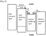
- Figure 2 illustrates an energy band diagram among a hole transport layer, a light-emitting layer, an electron buffering layer, and an electron transport zone of an organic electroluminescent device according to one embodiment of the present disclosure.
- a hole transport layer 123, a light-emitting layer 125, an electron buffering layer 126, and an electron transport zone 129 are sequentially stacked. Electrons (e) injected from a cathode are transported to a light-emitting layer through an electron transport zone 129 and an electron buffering layer 126.
- LUMO energy level of an electron buffering layer 126 may be higher than those of a host compound and a dopant compound of a light-emitting layer 125, and an electron transport layer 127. Specifically, LUMO energy levels may have the following relationship: the electron buffering layer > the electron transport zone > the host compound.
- HOMO energy level of an electron buffering layer 126 is higher than those of a host compound and a dopant compound of a light-emitting layer 125, but may be lower or higher than HOMO energy level of an electron transport zone 129.
- OLED was produced as follows. A transparent electrode indium tin oxide (ITO) thin film (15 ⁇ /sq) on a glass substrate for an OLED (Samsung Corning) was subjected to an ultrasonic washing with trichloroethylene, acetone, ethanol, and distilled water, sequentially, and then was stored in isopropanol. The ITO substrate was then mounted on a substrate holder of a vacuum vapor depositing apparatus.
- ITO indium tin oxide
- N 4 ,N 4' -diphenyl-N 4 ,N 4' -bis(9-phenyl-9H-carbazol-3-yl)-[1,1'-biphenyl]-4,4'-diamine was introduced into a cell of the vacuum vapor depositing apparatus, and then the pressure in the chamber of said apparatus was controlled to 10 -6 torr. Thereafter, an electric current was applied to the cell to evaporate the above introduced material, thereby forming a first hole injection layer having a thickness of 60 nm on the ITO substrate.
- 1,4,5,8,9,11-hexaazetriphenylene-hexacarbonitrile was then introduced into another cell of the vacuum vapor depositing apparatus, and was evaporated by applying an electric current to the cell, thereby forming a second hole injection layer having a thickness of 5 nm on the first hole injection layer.
- HT-1 N-([1,1'-biphenyl]-4-yl)-9,9-dimethyl-N-(4-(9-phenyl-9H-carbazol-3-yl)phenyl)-9H-fluoren-2-amine (HT-1) was then introduced into another cell of the vacuum vapor depositing apparatus, and was evaporated by applying an electric current to the cell, thereby forming a first hole transport layer having a thickness of 20 nm on the second hole injection layer. Thereafter, HT-2 was introduced into another cell of the vacuum vapor depositing apparatus, and was evaporated by applying an electric current to the cell, thereby forming a second hole transport layer having a thickness of 5 nm on the first hole transport layer.
- compound H-1 was introduced into one cell of the vacuum vapor depositing apparatus, as a host material, and compound D-38 was introduced into another cell as a dopant.
- the two materials were evaporated at different rates, so that the dopant was deposited in a doping amount of 2 wt% based on the total amount of the host and dopant to form a light-emitting layer having a thickness of 20 nm on the hole transport layer.
- 2-(4-(9,10-di(naphthalen-2-yl)anthracen-2-yl)phenyl)-1-phenyl-1H-benzo[d]imidazole was then introduced into one cell, and lithium quinolate was introduced into another cell.
- the two materials were evaporated at the same rate, so that they were respectively deposited in a doping amount of 50 wt% to form an electron transport layer having a thickness of 35 nm on the light-emitting layer.
- an Al cathode having a thickness of 80 nm was then deposited by another vacuum vapor deposition apparatus on the electron injection layer.
- All the material used for producing the OLED device were those purified by vacuum sublimation at 10 -6 torr.
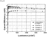
- Figure 3 shows a graph illustrating a current efficiency versus a luminance of the prepared organic electroluminescent device.
- luminous efficiency CIE color coordinate
- a driving voltage at 1,000 nit of luminance a driving voltage at 1,000 nit of luminance
- a lifespan for 10 hours at 2,000 nit and a constant current are shown in Table 1 below.
- OLEDs were produced and evaluated in the same manner as in Comparative Example 1, except that a thickness of an electron transport layer was 30 nm, and an electron buffering layer having a thickness of 5 nm was interposed between a light-emitting layer and an electron transport layer. Electron buffering materials used in Examples 1 to 3 are shown in Tables 1 and 4 below. Figure 3 shows a graph illustrating a current efficiency versus a luminance of the prepared organic electroluminescent device. In addition, evaluation results of the devices prepared in Examples 1 to 3 are shown in Table 1 below.
- OLEDs were produced and evaluated in the same manner as in Example 1, except that BF-1 and BF-65 were used for an electron buffering material and HT-3 was used for a second hole transport layer. Evaluation results of the devices prepared in Comparative Examples 2 and 3 were shown in Table 1 below.
- Table 1 Second Hole Transport Layer Electron Buffering Material Voltage (V) Current Efficiency (cd/A) Color coordinate (x) Color coordinate (y) Lifespan (hr) LUMO (eV) HOMO (eV) Comparative Ex. 1 HT-2 - 4.2 6.3 0.140 0.097 95.6 Comparative Ex. 2 HT-3 BF-1 4.5 6.6 0.140 0.095 95.4 1.95 5.48 Comparative Ex.
- the devices of Examples 1 to 3 show higher efficiencies and longer lifespan than those of Comparative Examples 1 to 3 in which an electron buffering layer is not comprised or an electron buffering material of the present disclosure is not used to prepare an electron buffering layer.
- LUMO energy levels of the electron buffering layer of Examples 1 to 3 were about 1.9 eV; LUMO energy level of the host compound was about 1.6 eV; and LUMO energy level of the electron transport layerwas about 1.8 eV. From Figure 3 , it is recognized that the organic electroluminescent devices of Examples 1 to 3 show higher current efficiencies over the whole range of luminance than the organic electroluminescent device of Comparative Example 1.
- OLEDs were produced in the same manner as in Comparative Example 1, except that a compound for a second hole transport layer was changed to HT-3 shown in Table 4 below.
- Luminous efficiency, CIE color coordinate, a driving voltage at 1,000 nit of luminance, and time taken for luminance to be reduced from 100% to 90% at 2,000 nit and a constant current are shown in Table 2 below.
- OLEDs were produced and evaluated in the same manner as in Comparative Example 4, except that a thickness of an electron transport layer was 30 nm, and an electron buffering layer having a thickness of 5 nm and comprising an electron buffering material was interposed between a light-emitting layer and an electron transport layer.
- Electron buffering materials used in Examples 4 to 8 are shown in Tables 2 and 4 below. Evaluation results of the devices prepared in Examples 4 to 8 are shown in Table 2 below. [Table 2] Second Hole Transport Layer Electron Buffering Material Voltage (V) Current Efficiency (cd/A) Color coordinate (x) Color coordinate (y) Lifespan (hr) LUMO (eV) HOMO (eV) Comparative Ex.
- Example 4 HT-3 - 4.1 6.5 0.139 0.094 27.9
- Example 4 HT-3 B-143 4.3 6.6 0.139 0.095 37.0 1.95 5.21
- Example 5 HT-3 B-145 4.4 6.9 0.139 0.096 47.3 1.90 5.43
- Example 6 HT-3 B-144 4.3 6.9 0.139 0.098 39.7 1.97 5.15
- Example 7 HT-3 B-147 4.3 6.8 0.139 0.095 35.1 1.89 5.40
- Example 8 HT-3 B-149 4.2 7.2 0.139 0.097 34.8 1.88 5.43
- the devices of Examples 4 to 8 have similar current characteristics to one of Comparative Example 4, but show higher efficiencies and longer lifespan than those of Comparative Example 4.
- OLEDs were produced and evaluated in the same manner as in Comparative Example 1, except that a thickness of a first hole transport layer was 10 nm; HT-4 was used to form a second hole transport layer having a thickness of 30 nm on a first hole transport layer; and H-44 and D-88 were used as a host and a dopant, respectively.
- the prepared OLED was evaluated as to luminous efficiency, CIE color coordinate, a driving voltage at 1,000 nit of luminance, and time taken for luminance to be reduced from 100% to 90% at 2,000 nit and a constant current, and the results are shown in Table 3 below.
- OLEDs were produced and evaluated in the same manner as in Comparative Example 5, except that a thickness of an electron transport layer was 30 nm, and an electron buffering layer having a thickness of 5 nm and comprising an electron buffering material was interposed between a light-emitting layer and an electron transport layer. Electron buffering materials used in Examples 9 and 10 are shown in Table 3 below, along with evaluation results of the prepared devices. [Table 3] Second Hole Transport Layer Electron Buffering Material Voltage (V) Current Efficiency (cd/A) Color coordinate (x) Color coordinate (y) Lifespan (hr) LUMO (eV) HOMO (eV) Comparative Ex.
- OLEDs were produced in the same manner as in Example 1, except that compounds shown in Table 5 below were used as an electron buffering material.
- the electron buffering layer was formed by a co-evaporation of the two compounds shown in Table 5.
- the prepared OLEDs were evaluated as to luminous efficiency, CIE color coordinate, a driving voltage at 1,000 nit of luminance, and lifespan for 10 hours at 2,000 nit and a constant current, and the results are shown in Table 5 below.
- OLEDs were produced in the same manner as in Example 1, except that compounds shown in Table 6 below were used as an electron buffering material.
- the electron buffering layer of Example 17 was formed by a co-evaporation, while the electron buffering layer of Example 18 was formed by a mixture-evaporation.
- the prepared OLEDs were evaluated as to luminous efficiency, CIE color coordinate, a driving voltage at 1,000 nit of luminance, and lifespan for 10 hours at 2,000 nit and a constant current, and the results are shown in Table 6 below.
- Example 17 shows that due to speediness of electron current by the electron buffering material of the present disclosure, the devices of Examples 17 and 18 show higher efficiency than those of Comparative Examples 1 to 3 shown in Table 1 in which an electron buffering layer was not comprised or an electron buffering material of the present disclosure is not used to prepare an electro buffer layer. In particular, lifespan was significantly enhanced by 97.4%. Furthermore, B-145 and BF-6 have the same deposition temperature, and thus are suitable for a mixture-evaporation. Example 18 shows that an electron buffering layer can be formed by a mixture-evaporation with the material. A respective deposition temperature of the compounds in a vacuum vapor depositing apparatus are shown in Table 7 below.
- the mixture-evaporation method for an electron buffering layer has an advantage in that device characteristics can be maintained until the whole material is consumed in a crucible.
Landscapes
- Chemical & Material Sciences (AREA)
- Organic Chemistry (AREA)
- Engineering & Computer Science (AREA)
- Materials Engineering (AREA)
- Physics & Mathematics (AREA)
- Spectroscopy & Molecular Physics (AREA)
- Optics & Photonics (AREA)
- Electroluminescent Light Sources (AREA)
- Plural Heterocyclic Compounds (AREA)
Abstract
Description
- The present disclosure relates to an electron buffering material and an organic electroluminescent device.
- An organic electroluminescent device (OLED) emitting green light was first proposed by Tang et al. of Eastman Kodak in 1987, which employs a double layer of TPD/Alq3, composed of a light-emitting layer and a charge transport layer. Afterward, an organic electroluminescent device had been rapidly researched, and has now become commercialized. At present, a phosphorescent material, which has excellent luminous efficiency, is mainly used for a panel of an organic electroluminescent device. An organic electroluminescent device emitting red or green light has been successfully commercialized by using a phosphorous material. However, a phosphorous material for emitting blue light has the following disadvantages, which are blocking realization of full color display: roll-off is reduced at high current due to loss of excessively formed excitons, thereby deteriorating performances; the blue-emitting phosphorous material itself has a problem in long term stability of lifespan; and color purity is rapidly decreasing by lapse of time.
- A fluorescent material has been used until the present, but has several problems. First, when exposed to high-temperature during a panel production process, a current feature can be changed, which can cause a change in luminance. Furthermore, due to a structural characteristic, an interface feature between a light-emitting layer and an electron injection layer can deteriorate, which can cause a decrease of luminance. In addition, a fluorescent material provides lower efficiencies than a phosphorescent material. Accordingly, there have been attempts to improve efficiencies by developing a specific fluorescent material such as a combination of an anthracene-based host and a pyrene-based dopant. However, the proposed combination makes holes become greatly trapped, which can cause light-emitting sites in a light-emitting layer to shift to the side close to a hole transport layer, thereby light being emitted at an interface. The light-emission at an interface decreases lifespan of a device, and efficiencies are not satisfactory.
- It is not easy to solve the aforementioned problems of a fluorescent material by improvement of a light-emitting material itself. Accordingly, recently, there has been research to solve the problems, which include improvement of a charge transport material to change a charge transport feature, and a development of optimized device structure.
- Korean Patent Application Laying-Open No.
10-2012-0092550 - The objective of the present disclosure is to provide an electron buffering material which can provide an organic electroluminescent device having low driving voltage, excellent luminous efficiency, and long lifespan; and an organic electroluminescent device comprising the electron buffering material.
- The present inventors found that the objective above can be achieved by an electron buffering material comprising a compound represented by the following
formula 1; and an organic electroluminescent device comprising a first electrode, a second electrode facing the first electrode, a light-emitting layer between the first electrode and the second electrode, and an electron transport zone and an electron buffering layer between the light-emitting layer and the second electrode, wherein the electron buffering layer comprises a compound represented by the followingformula 1.
- A represents a substituted or unsubstituted (5- to 30-membered)heteroaryl;
- L represents a single bond, a substituted or unsubstituted (C6-C30)arylene, or a substituted or unsubstituted (5- to 30-membered)heteroarylene;
- R1 represents the following formula 2a or 2b:

- R2 represents hydrogen, deuterium, a halogen, a cyano, a substituted or unsubstituted (C1-C30)alkyl, a substituted or unsubstituted (C6-C30)aryl, a substituted or unsubstituted (5-to 30-membered)heteroaryl, a substituted or unsubstituted (C3-C30)cycloalkyl, a substituted or unsubstituted (C1-C30)alkoxy, a substituted or unsubstituted tri(C1-C30)alkylsilyl, a substituted or unsubstituted tri(C6-C30)arylsilyl, a substituted or unsubstituted di(C1-C30)alkyl(C6-C30)arylsilyl, a substituted or unsubstituted (C1-C30)alkyldi(C6-C30)arylsilyl, a substituted or unsubstituted mono- or di-(C1-C30)alkylamino, a substituted or unsubstituted mono- or di-(C6-C30)arylamino, a substituted or unsubstituted (C1-C30)alkyl(C6-C30)arylamino, or the
following formula 3; or may be fused with the carbazole backbone to form a substituted or unsubstituted benzocarbazole;
- X represents O, S, CR11R12, NR13 or SiR13R14;
- R3 represents hydrogen, deuterium, a halogen, a cyano, a substituted or unsubstituted (C1-C30)alkyl, a substituted or unsubstituted (C6-C30)aryl, a substituted or unsubstituted (5-to 30-membered)heteroaryl, a substituted or unsubstituted (C3-C30)cycloalkyl, a substituted or unsubstituted (C1-C30)alkoxy, a substituted or unsubstituted tri(C1-C30)alkylsilyl, a substituted or unsubstituted tri(C6-C30)arylsilyl, a substituted or unsubstituted di(C1-C30)alkyl(C6-C30)arylsilyl, a substituted or unsubstituted (C1-C30)alkyldi(C6-C30)arylsilyl, a substituted or unsubstituted mono- or di-(C1-C30)alkylamino, a substituted or unsubstituted mono- or di-(C6-C30)arylamino, or a substituted or unsubstituted (C1-C30)alkyl(C6-C30)arylamino;
- R4, R5, R7 and R10, each independently, represent hydrogen, deuterium, a halogen, a cyano, a substituted or unsubstituted (C1-C30)alkyl, a substituted or unsubstituted (C6-C30)aryl, a substituted or unsubstituted (5- to 30-membered)heteroaryl, a substituted or unsubstituted (C3-C30)cycloalkyl, a substituted or unsubstituted (C1-C30)alkoxy, a substituted or unsubstituted tri(C1-C30)alkylsilyl, a substituted or unsubstituted tri(C6-C30)arylsilyl, a substituted or unsubstituted di(C1-C30)alkyl(C6-C30)arylsilyl, a substituted or unsubstituted (C1-C30)alkyldi(C6-C30)arylsilyl, a substituted or unsubstituted mono- or di-(C1-C30)alkylamino, a substituted or unsubstituted mono- or di-(C6-C30)arylamino, or a substituted or unsubstituted (C1-C30)alkyl(C6-C30)arylamino; or may be linked to an adjacent substituent(s) to form a substituted or unsubstituted (C3-C30), mono- or polycyclic, alicyclic or aromatic ring whose carbon atom(s) may be replaced with at least one hetero atom selected from nitrogen, oxygen, and sulfur;
- R6, R8 and R9, each independently, represent a substituted or unsubstituted (C1-C30)alkyl, a substituted or unsubstituted (C6-C30)aryl, a substituted or unsubstituted (5- to 30-membered)heteroaryl, a substituted or unsubstituted (C3-C30)cycloalkyl, a substituted or unsubstituted mono- or di-(C1-C30)alkylamino, a substituted or unsubstituted mono- or di-(C6-C30)arylamino, or a substituted or unsubstituted (C1-C30)alkyl(C6-C30)arylamino;
- R11 to R14, each independently, represent a substituted or unsubstituted (C1-C30)alkyl, a substituted or unsubstituted (C6-C30)aryl, or a substituted or unsubstituted (5- to 30-membered)heteroaryl; or may be linked to an adjacent substituent(s) to form a substituted or unsubstituted (C3-C30), mono- or polycyclic, alicyclic or aromatic ring whose carbon atom(s) may be replaced with at least one hetero atom selected from nitrogen, oxygen, and sulfur;
- a, c, d, e, and f, each independently, represent an integer of 0 to 4; where a, c, d, e, or f is an integer of 2 or more, each of R2, R4, R5, R7 or R10 may be the same or different;
- b represents an integer of 0 to 3; where b is an integer of 2 or more, each of R3 may be the same or different;
- n represents an integer of 0 or 1; m represents an integer of 1 or 2;
- * represents a bonding site to the carbazole backbone; and
- the heteroaryl(ene) contains one or more hetero atoms selected from B, N, O, S, P(=O), Si, and P.
- By using the electron buffering material of the present disclosure, an organic electroluminescent device can have low driving voltage, excellent luminous efficiency, and long lifespan.
-
-
Fig. 1 is a schematic sectional view illustrating a structure of an organic electroluminescent device according to one embodiment of the present disclosure; -
Fig. 2 is an energy band diagram among a hole transport layer, a light-emitting layer, an electron buffering layer, and an electron transport zone of an organic electroluminescent device according to one embodiment of the present disclosure; and -
Fig. 3 is a graph illustrating a current efficiency versus a luminance of organic electroluminescent devices of Examples 1 to 3, and Comparative Example 1. - Hereinafter, the present disclosure will be described in detail. However, the following description is intended to explain the invention, and is not meant in any way to restrict the scope of the invention.
- LUMO ("Lowest Unoccupied Molecular Orbital") and HOMO ("Highest Occupied Molecular Orbital") have negative energy levels. However, for convenience, LUMO energy level and HOMO energy level are indicated by absolute values in the present disclosure. Thus, upon comparison between the LUMO energy level and the HOMO energy level, the comparison is conducted on the basis of their absolute values. In the present disclosure, the LUMO energy level and the HOMO energy level are calculated by Density Functional Theory (DFT).
- Herein, "(C1-C30)alkyl(ene)" indicates a linear or branched alkyl(ene) having 1 to 30, preferably 1 to 20, and more preferably 1 to 10 carbon atoms, and includes methyl, ethyl, n-propyl, isopropyl, n-butyl, isobutyl, tert-butyl, etc. "(C2-C30) alkenyl" indicates a linear or branched alkenyl having 2 to 30, preferably 2 to 20, and more preferably 2 to 10 carbon atoms and includes vinyl, 1-propenyl, 2-propenyl, 1-butenyl, 2-butenyl, 3-butenyl, 2-methylbut-2-enyl, etc. "(C2-C30)alkynyl" indicates a linear or branched alkynyl having 2 to 30, preferably 2 to 20, and more preferably 2 to 10 carbon atoms and includes ethynyl, 1-propynyl, 2-propynyl, 1-butynyl, 2-butynyl, 3-butynyl, 1-methylpent-2-ynyl, etc. "(C3-C30)cycloalkyl" indicates a mono- or polycyclic hydrocarbon having 3 to 30, preferably 3 to 20, and more preferably 3 to 7 carbon atoms and includes cyclopropyl, cyclobutyl, cyclopentyl, cyclohexyl, etc. "(3- to 7-membered) heterocycloalkyl" indicates a cycloalkyl having 3 to 7, preferably 5 to 7 ring backbone atoms including at least one hetero atom selected from B, N, O, S, P(=O), Si, and P, preferably O, S, and N, and includes tetrahydrofuran, pyrrolidine, thiolan, tetrahydropyran, etc. Furthermore, "(C6-C30)aryl(ene)" indicates a monocyclic or fused ring derived from an aromatic hydrocarbon and having 6 to 30, preferably 6 to 20, and more preferably 6 to 15 ring backbone carbon atoms, and includes phenyl, biphenyl, terphenyl, naphthyl, binaphthyl, phenylnaphthyl, naphthylphenyl, fluorenyl, phenylfluorenyl, benzofluorenyl, dibenzofluorenyl, phenanthrenyl, phenylphenanthrenyl, anthracenyl, indenyl, triphenylenyl, pyrenyl, tetracenyl, perylenyl, chrysenyl, naphthacenyl, fluoranthenyl, spirofluorenyl, etc. "(5- to 30-membered) heteroaryl(ene)" indicates an aryl group having 5 to 30 ring backbone atoms including at least one, preferably 1 to 4, hetero atom selected from the group consisting of B, N, O, S, P(=O), Si, and P; may be a monocyclic ring, or a fused ring condensed with at least one benzene ring; may be partially saturated; may be one formed by linking at least one heteroaryl or aryl group to a heteroaryl group via a single bond(s); and includes a monocyclic ring-type heteroaryl such as furyl, thiophenyl, pyrrolyl, imidazolyl, pyrazolyl, thiazolyl, thiadiazolyl, isothiazolyl, isoxazolyl, oxazolyl, oxadiazolyl, triazinyl, tetrazinyl, triazolyl, tetrazolyl, furazanyl, pyridyl, pyrazinyl, pyrimidinyl, pyridazinyl, etc., and a fused ring-type heteroaryl such as benzofuranyl, benzothiophenyl, isobenzofuranyl, dibenzofuranyl, dibenzothiophenyl, benzonaphthofuranyl, benzonaphthothiophenyl, benzoimidazolyl, benzothiazolyl, benzoisothiazolyl, benzoisoxazolyl, benzoxazolyl, isoindolyl, indolyl, indazolyl, benzothiadiazolyl, quinolyl, isoquinolyl, cinnolinyl, quinazolinyl, quinoxalinyl, naphthyridinyl, carbazolyl, benzocarbazolyl, phenoxazinyl, phenanthridinyl, benzodioxolyl, dihydroacridinyl, etc. Furthermore, "halogen" includes F, CI, Br, and I.
- Herein, "substituted" in the expression, "substituted or unsubstituted," means that a hydrogen atom in a certain functional group is replaced with another atom or group, i.e. a substituent. The substituents of the substituted (C1-C30)alkyl, the substituted (C1-C30)alkoxy, the substituted (C3-C30)cycloalkyl, the substituted (C6-C30)aryl(ene), the substituted (5- to 30-membered)heteroaryl(ene) and the substituted (C6-C30)aryl(C1-C30)alkyl in A, L, and R2 to R14 of
formula 1 of the present disclosure, each independently, are at least one selected from the group consisting of deuterium, a halogen, a cyano, a carboxy, a nitro, a hydroxy, a (C1-C30)alkyl, a halo(C1-C30)alkyl, a (C2-C30)alkenyl, a (C2-C30)alkynyl, a (C1-C30)alkoxy, a (C1-C30)alkylthio, a (C3-C30)cycloalkyl, a (C3-C30)cycloalkenyl, a (3- to 7-membered)heterocycloalkyl, a (C6-C30)aryloxy, a (C6-C30)arylthio, a (3- to 30-membered)heteroaryl unsubstituted or substituted with a (C6-C30)aryl, a (C6-C30)aryl unsubstituted or substituted with a (3- to 30-membered)heteroaryl, a tri(C1-C30)alkylsilyl, a tri(C6-C30)arylsilyl, a di(C1-C30)alkyl(C6-C30)arylsilyl, a (C1-C30)alkyldi(C6-C30)arylsilyl, an amino, a mono- or di-(C1-C30)alkylamino, a mono- or di-(C6-C30)arylamino, a (C1-C30)alkyl(C6-C30)arylamino, a (C1-C30)alkylcarbonyl, a (C1-C30)alkoxycarbonyl, a (C6-C30)arylcarbonyl, a di(C6-C30)arylboronyl, a di(C1-C30)alkylboronyl, a (C1-C30)alkyl(C6-C30)arylboronyl, a (C6-C30)aryl(C1-C30)alkyl, and a (C1-C30)alkyl(C6-C30)aryl; and preferably, each independently, are at least one selected from the group consisting of a (C1-C30)alkyl, a (3- to 30-membered)heteroaryl unsubstituted or substituted with a (C6-C30)aryl, a (C6-C30)aryl unsubstituted or substituted with a (3- to 30-membered)heteroaryl, a (C6-C30)aryl(C1-C30)alkyl, and a (C1-C30)alkyl(C6-C30)aryl. - According to one aspect of the present disclosure, an electron buffering material comprising the compound represented by
formula 1 is provided. The electron buffering material indicates a material controlling an electron flow. Therefore, the electron buffering material may be, for example, a material trapping electrons, blocking electrons, or lowering an energy barrier between an electron transport zone and a light-emitting layer. Specifically, the electron buffering material may be for an organic electroluminescent device. In the organic electroluminescent device, the electron buffering material may be used for preparing an electron buffering layer, or may be added to another area such as an electron transport zone or a light-emitting layer. The electron buffering layer may be formed between a light-emitting layer and an electron transport zone, or between an electron transport zone and a second electrode of an organic electroluminescent device. The electron buffering material may be a mixture or composition which may further comprise a conventional material for preparing an organic electroluminescent device. - The compound of
formula 1 may be represented, preferably, by any one of the following formulae 4 to 10, and specifically, by the following formula 4, 5, or 7.


formula 1. - In
formulae 1 and 4 to 10, A may represent preferably, a substituted or unsubstituted nitrogen-containing (5- to 30-membered)heteroaryl; and, more preferably, a substituted or unsubstituted nitrogen-containing (6- to 20-membered)heteroaryl. Specifically, A may represent a substituted or unsubstituted pyridyl, a substituted or unsubstituted pyrimidinyl, a substituted or unsubstituted triazinyl, a substituted or unsubstituted pyrazinyl, a substituted or unsubstituted quinolyl, a substituted or unsubstituted isoquinolyl, a substituted or unsubstituted quinolinyl, a substituted or unsubstituted quinazolinyl, a substituted or unsubstituted quinoxalinyl, or a substituted or unsubstituted naphthyridinyl; and more specifically, a substituted or unsubstituted pyridyl, a substituted or unsubstituted pyrimidinyl, a substituted or unsubstituted triazinyl, or a substituted or unsubstituted pyrazinyl. Preferably, the substituent of the substituted heteroaryl of A may be at least one selected from the group consisting of a (C1-C10)alkyl; a (C6-C20)aryl unsubstituted or substituted with deuterium, a cyano, a halogen, a (C1-C10)alkyl, a (C6-C20)cycloalkyl, a (C6-C20)aryl, a (6- to 20-membered)heteroaryl, a di(C6-C20)arylamino, or a tri(C6-C20)arylsilyl; and, a (6- to 20-membered)heteroaryl unsubstituted or substituted with deuterium, a cyano, a halogen, a (C1-C10)alkyl, a (C6-C20)cycloalkyl, a (C6-C20)aryl, a (6- to 20-membered)heteroaryl, a di(C6-C20)arylamino, or a tri(C6-C20)arylsilyl. - In
formulae 1 and 4 to 10, L may represent preferably, a single bond or a substituted or unsubstituted (C6-C20)arylene; and more preferably, a single bond or an unsubstituted (C6-C18)arylene. Specifically, L may represent a single bond, a substituted or unsubstituted phenyl, a substituted or unsubstituted naphthyl, a substituted or unsubstituted biphenyl, a substituted or unsubstituted terphenyl, a substituted or unsubstituted phenylnaphthyl, or a substituted or unsubstituted naphthylphenyl. - In
formulae 1 and 4 to 10, R2 may represent preferably, hydrogen, deuterium, a substituted or unsubstituted (C6-C20)aryl, a substituted or unsubstituted (5- to 20-membered)heteroaryl, a substituted or unsubstituted mono- or di-(C6-C20)arylamino, orformula 3, or may be fused with the carbazole backbone to form a substituted or unsubstituted benzocarbazole. Specifically, R2 may represent hydrogen, or a substituted or unsubstituted (C6-C20)aryl. More specifically, R2 may represent hydrogen, a substituted or unsubstituted phenyl, a substituted or unsubstituted dibenzothiophenyl, a substituted or unsubstituted dibenzofuranyl, a substituted or unsubstituted carbazolyl, a substituted or unsubstituted diphenylamino, a substituted or unsubstituted fluorenyl, orformula 3, or may be fused with the carbazole backbone to form a substituted or unsubstituted benzocarbazole. - In
formula 3, X may represent preferably, O, S, CR11R12, or NR13. R10 may represent preferably, hydrogen or a (C1-C20)alkyl. R11 to R14, each independently, may represent preferably, hydrogen, a substituted or unsubstituted (C1-C10)alkyl, a substituted or unsubstituted (C6-C20)aryl, or a substituted or unsubstituted (5- to 20-membered)heteroaryl; and specifically, hydrogen, a (C1-C6)alkyl, phenyl, naphthyl, or biphenyl. - In
formulae 1 and 4 to 10, R3, R4, R5, and R7, each independently, may represent preferably, hydrogen or a substituted or unsubstituted (C1-C20)alkyl. Specifically, R3, R4, R5, and R7 may represent hydrogen. - In
formulae 1 and 4 to 10, R6, R8, and R8, each independently, may represent preferably, a substituted or unsubstituted (C1-C20)alkyl, a substituted or unsubstituted (C6-C20)aryl, or a substituted or unsubstituted (6- to 20-membered)heteroaryl; and more preferably, a substituted or unsubstituted (C6-C20)aryl. Specifically, R6, R8, and Rg, each independently, may represent a substituted or unsubstituted phenyl, a substituted or unsubstituted biphenyl, or a substituted or unsubstituted naphthyl. - In
formulae 1 and 4 to 10, specifically, a may represent 0 or 1; b may represent 0; c, d, e, and f, each independently, may represent an integer of 0 to 2; n may represent 0 or 1; and m may represent 1. - According to one embodiment of the present disclosure, A represents a substituted or unsubstituted nitrogen-containing (5- to 30-membered)heteroaryl; L represents a single bond or a substituted or unsubstituted (C6-C20)arylene; R1 represents formula 2a or 2b; R2 represents hydrogen, deuterium, a substituted or unsubstituted (C6-C20)aryl, a substituted or unsubstituted (5- to 20-membered)heteroaryl, a substituted or unsubstituted mono- or di-(C6-C20)arylamino or formula 3, or is fused with the carbazole backbone to form a substituted or unsubstituted benzocarbazole; X represents O, S, CR11R12, or NR13; R10 represents hydrogen or a (C1-C20)alkyl; R3, R4, R5, and R7, each independently, represent hydrogen or a substituted or unsubstituted (C1-C20)alkyl; R6, R8 and Rg, each independently, represent a substituted or unsubstituted (C1-C20)alkyl, a substituted or unsubstituted (C6-C20)aryl, or a substituted or unsubstituted (6- to 20-membered)heteroaryl; R11 to R14, each independently, represent hydrogen, a substituted or unsubstituted (C1-C10)alkyl, a substituted or unsubstituted (C6-C20)aryl, or a substituted or unsubstituted (5- to 20-membered)heteroaryl; and the heteroaryl contains one or more hetero atoms selected from N, O, and S.
- Specifically, the compound of
formula 1 includes the following, but is not limited thereto.





- The compound of the present disclosure can be prepared by a synthetic method known to one skilled in the art. For example, it can be prepared according to the following
reaction scheme 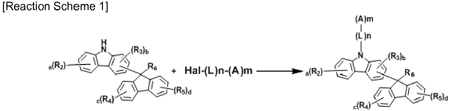


- In
reaction schemes formula 1, and Hal represents a halogen. For more specific methods for preparing the compound of the present disclosure, please refer to Korean Patent Application No.2013-0149733 - The electron buffering material may further comprise a compound represented by the following formula 11.

- Ar5 and Ar6, each independently, represent a substituted or unsubstituted (5- to 30-membered)heteroaryl, or a substituted or unsubstituted (C6-C30)aryl;
- L' represents a single bond, a substituted or unsubstituted (C6-C30)arylene, or a substituted or unsubstituted (3- to 30-membered)heteroarylene;
- X1 to X3, each independently, represent N or C, with the proviso that at least one of X1 to X3 represents N;
- R15 and R16, each independently, represent hydrogen, deuterium, a halogen, a cyano, a carboxy, a nitro, a hydroxy, a substituted or unsubstituted (C1-C30)alkyl, a substituted or unsubstituted (C6-C30)aryl, a substituted or unsubstituted (5- to 30-membered)heteroaryl, a substituted or unsubstituted (C3-C30)cycloalkyl, a substituted or unsubstituted (C3-C30)cycloalkenyl, a substituted or unsubstituted (3- to 7-membered)heterocycloalkyl, a substituted or unsubstituted (C1-C30)alkoxy, a substituted or unsubstituted tri(C1-C30)alkylsilyl, a substituted or unsubstituted tri(C6-C30)arylsilyl, a substituted or unsubstituted di(C1-C30)alkyl(C6-C30)arylsilyl, a substituted or unsubstituted (C1-C30)alkyldi(C6-C30)arylsilyl, a substituted or unsubstituted mono- or di-(C1-C30)alkylamino, a substituted or unsubstituted mono- or di-(C6-C30)arylamino, or a substituted or unsubstituted (C1-C30)alkyl(C6-C30)arylamino, or may be linked to an adjacent substituent(s) to form a substituted or unsubstituted (C3-C30), mono- or polycyclic, alicyclic or aromatic ring whose carbon atom(s) may be replaced with at least one hetero atom selected from nitrogen, oxygen, and sulfur;
- the heteroaryl(ene) and heterocycloalkyl, each independently, contain one or more hetero atoms selected from B, N, O, S, P(=O), Si and P; and
- s and t, each independently, represent an integer of 1 to 4; where s or t is an integer of 2 or more, each of R15 or R16 may be the same or different.
- In formula 11, preferably, Ar5 and Ar6, each independently, may represent a substituted or unsubstituted (6- to 20-membered)heteroaryl, or a substituted or unsubstituted (C6-C20)aryl. Specifically, Ar5 and Ar6, each independently, represent a substituted or unsubstituted phenyl, a substituted or unsubstituted biphenyl, a substituted or unsubstituted naphthyl, a substituted or unsubstituted terphenyl, a substituted or unsubstituted phenylnaphthyl, a substituted or unsubstituted naphthylphenyl, a substituted or unsubstituted anthracenyl, a substituted or unsubstituted phenanthrenyl, a substituted or unsubstituted fluorenyl, a substituted or unsubstituted carbazolyl, a substituted or unsubstituted dibenzothiophenyl, or a substituted or unsubstituted dibenzofuranyl. Preferably, the substituents of the substituted heteroaryl and the substituted aryl in Ar5 and Ar6, each independently, may be a (C1-C10)alkyl, a (C6-C20)aryl, a (6- to 20-membered)heteroaryl, or a di(C6-C20)arylamino.
- In formula 11, preferably, L' may represent a single bond, or a substituted or unsubstituted (C6-C20)arylene. Specifically, L' may represent a single bond, a substituted or unsubstituted phenylene, a substituted or unsubstituted naphthylene, or a substituted or unsubstituted biphenylene.
- In formula 11, preferably, R15 and R16, each independently, may represent hydrogen, a substituted or unsubstituted (C6-C20)aryl, or a substituted or unsubstituted (5- to 20-membered)heteroaryl, or may be linked to an adjacent substituent(s) to form a substituted or unsubstituted (C5-C20), mono- or polycyclic aromatic ring whose carbon atom(s) may be replaced with at least one hetero atom selected from nitrogen, oxygen, and sulfur; and s and t represent 1. In formula 11, R15 and R16 may not be a substituted or unsubstituted fluorenyl. In formula 11, R15 and R16, each independently, may not form a substituted or unsubstituted fluorene ring with a benzene ring of the carbazole backbone linked to R15 and R16. Specifically, R15 and R16, each independently, may represent hydrogen, a substituted or unsubstituted phenyl, a substituted or unsubstituted naphthyl, a substituted or unsubstituted biphenyl, a substituted or unsubstituted dibenzothiophenyl, a substituted or unsubstituted dibenzofuranyl, or a substituted or unsubstituted carbazolyl, or may be linked to an adjacent substituent(s) to form a substituted or unsubstituted benzene ring, a substituted or unsubstituted indene ring, a substituted or unsubstituted indole ring, a substituted or unsubstituted benzothiophene ring, or a substituted or unsubstituted benzofuran ring. Preferably, the substituents of the substituted groups such as the substituted heteroaryl and the substituted aryl in R15 and R16, each independently, may be a (C1-C10)alkyl, a (C6-C20)aryl, a (6- to 20-membered)heteroaryl unsubstituted or substituted with a (C6-C20)aryl, a di(C6-C20)arylamino, or a tri(C6-C20)arylsilyl.
- According to one embodiment of the present disclosure, Ar5 and Ar6, each independently, may represent a substituted or unsubstituted (6- to 20-membered)heteroaryl, or a substituted or unsubstituted (C6-C20)aryl; L' represents a single bond, or a substituted or unsubstituted (C6-C20)arylene; R15 and R16, each independently, represent hydrogen, a substituted or unsubstituted (C6-C20)aryl, or a substituted or unsubstituted (5- to 20-membered)heteroaryl, or may be linked to an adjacent substituent(s) to form a substituted or unsubstituted (C5-C20), mono- or polycyclic aromatic ring whose carbon atom(s) may be replaced with at least one hetero atom selected from nitrogen, oxygen, and sulfur; and s and t may represent 1.
- Specifically, the compound of formula 11 includes the following, but is not limited thereto:


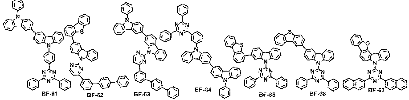


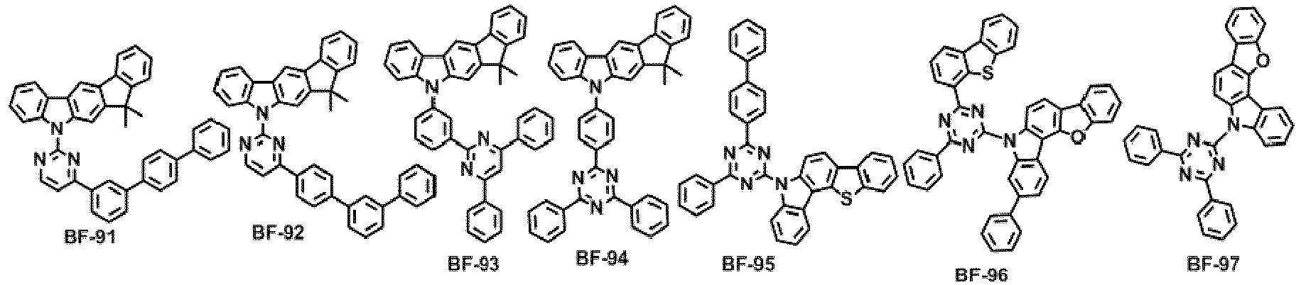
- According to another aspect of the present disclosure, it is provided an organic electroluminescent device comprising a first electrode, a second electrode facing the first electrode, a light-emitting layer between the first electrode and the second electrode, and an electron transport zone and an electron buffering layer between the light-emitting layer and the second electrode, wherein the electron buffering layer comprises the compound represented by
formula 1 above. - By interposing the electron buffering layer between the light-emitting layer and the second electrode in the organic electroluminescent device comprising the first and second electrodes and the light-emitting layer, an electron injection can be controlled by electron affinity LUMO energy of the electron buffering layer.
- The electron buffering layer in the organic electroluminescent device may further comprise the compound of formula 11, in addition to the compound of
formula 1. The weight ratio between the compound offormula 1 and compound of formula 11 is in the range of 1:99 to 99:1, preferably 10:90 to 90:10, and more preferably 30:70 to 70:30 in view of driving voltage and luminous efficiency. - When the electron buffering layer comprises both the compound of
formula 1 and the compound of formula 11, these compounds for the electron buffering layer may be co-evaporated or mixture-evaporated. Herein, a co-evaporation indicates a process for two or more materials to be deposited as a mixture, by introducing each of the two or more materials into respective crucible cells, and applying electric current to the cells for each of the materials to be evaporated. Herein, a mixture-evaporation indicates a process for two or more materials to be deposited as a mixture, by mixing the two or more materials in one crucible cell before the deposition, and applying electric current to the cell for the mixture to be evaporated. - In the organic electroluminescent device, a light-emitting layer may comprise a host compound and a dopant compound. The host compound may be a phosphorescent host compound or a fluorescent host compound. The dopant compound may be a phosphorescent dopant compound or a fluorescent dopant compound. Preferably, the host compound and the dopant compound may be a fluorescent host compound and a fluorescent dopant compound, respectively. LUMO energy level of the electron buffering layer may be higher than LUMO energy level of the host compound. Specifically, the difference in LUMO energy levels between the electron buffering layer and the host compound may be 0.7 eV or less. For example, LUMO energy levels of the electron buffering layer and the host compound may be 1.9 eV and 1.6 eV, respectively, and thus the difference in LUMO energy level may be 0.3 eV. Although LUMO barrier between the host compound and the electron buffering layer can cause an increase in driving voltage, electrons can be more easily transferred to the host compound due to the compound of
formula 1 comprised in the electron buffering layer. Therefore, the organic electroluminescent device of the present disclosure can have low driving voltage, high luminous efficiency, and long lifespan. Herein, specifically, LUMO energy level of an electron buffering layer may indicate the level of the compound offormula 1 comprised in the electron buffering layer. - LUMO energy level of the electron buffering layer may be preferably in the range of 1.6 to 2.3 eV, and more preferably in the range of 1.75 to 2.05 eV. When LUMO energy level of the electron buffering layer is in the range as above, electrons cannot be easily injected to another layer. However, if the electron buffering layer comprises the compound of
formula 1, the organic electroluminescent device can have low driving voltage, high luminous efficiency, and long lifespan. - In the organic electroluminescent device of the present disclosure, the electron transport zone indicates a zone transporting electrons from the second electrode to the light-emitting layer. The electron transport zone may comprise an electron transport compound, a reductive dopant, or a combination thereof. The electron transport compound may be at least one selected from the group consisting of oxazole-based compounds, isoxazole-based compounds, triazole-based compounds, isothiazole-based compounds, oxadiazole-based compounds, thiadiazole-based compounds, perylene-based compounds, anthracene-based compounds, aluminum complexes, and gallium complexes. The reductive dopant may be at least one selected from the group consisting of alkali metals, alkali metal compounds, alkaline earth metals, rare-earth metals, and halides, oxides, and complexes thereof. The electron transport zone may comprise an electron transport layer, an electron injection layer, or both of them. The electron transport layer and the electron injection layer, each independently, may be composed of two or more layers. LUMO energy level of the electron buffering layer may be higher or lower than LUMO energy level of the electron transport zone. For example, the electron buffering layer and the electron transport zone may have LUMO energy levels of 1.9 eV and 1.8 eV, respectively, and a difference between them in LUMO energy level may be 0.1 eV. When the electron buffering layer has LUMO energy level as in said numerical range, electrons can be easily injected to a light-emitting layer through the electron buffering layer. LUMO energy level of the electron transport zone may be 1.7 eV or more, or 1.9 eV or more. In the present disclosure, specifically, LUMO energy level of the electron transport zone may indicate the level of an electron transport material comprised in the electron transport zone. When the electron transport zone has two or more layers, LUMO energy level of the electron transport zone may be the one of a material comprised in a layer which is in the electron transport zone and is adjacent to the electron buffering layer.
- Specifically, LUMO energy level of the electron buffering layer may be higher than those of the host compound and the electron transport zone. For example, LUMO energy levels may have the following relationship: the electron buffering layer > the electron transport zone > the host compound. According to the aforementioned LUMO relationship, electrons are trapped between the light-emitting layer and the electron buffering layer, which inhibits an injection of electrons to a light-emitting layer, and thus can cause an increase in driving voltage. However, an electron buffering layer comprising the compound of
formula 1 can easily transport electrons to the light-emitting layer, and thus the organic electroluminescent device of the present disclosure can have low driving voltage, high luminous efficiency, and long lifespan. - LUMO energy level can be easily measured by known various methods. Generally, cyclic voltametry or ultraviolet photoelectron spectroscopy (UPS) may be used. Therefore, one skilled in the art can easily understand and determine the electron buffering layer, the host material, and the electron transport zone which satisfy the aforementioned relationship for LUMO energy levels, so that he/she can easily practice the invention. HOMO energy level can be easily measured in the same manner as LUMO energy level.
- The layers of the organic electroluminescent device of the present disclosure can be formed in the order of the light-emitting layer, the electron buffering layer, the electron transport zone, and the second electrode, or in the order of the light-emitting layer, the electron transport zone, the electron buffering layer, and the second electrode.
- Hereinafter, referring to
Figure 1 , the structure of an organic electroluminescent device, and a method for preparing it will be described in detail. -
Figure 1 shows anorganic electroluminescent device 100 comprising asubstrate 101, afirst electrode 110 formed on thesubstrate 101, anorganic layer 120 formed on thefirst electrode 110, and asecond electrode 130 formed on theorganic layer 120 and facing thefirst electrode 110. - The
organic layer 120 comprises ahole injection layer 122, ahole transport layer 123 formed on thehole injection layer 122, a light-emittinglayer 125 formed on thehole transport layer 123, anelectron buffering layer 126 formed on the light-emittinglayer 125, and anelectron transport zone 129 formed on theelectron buffering layer 126; and theelectron transport zone 129 comprises anelectron transport layer 127 formed on theelectron buffering layer 126, and anelectron injection layer 128 formed on theelectron transport layer 127. - The
substrate 101 may be any conventional substrate for an organic electroluminescent device, such as a glass substrate, a plastic substrate, or a metal substrate. - The
first electrode 110 may be an anode, and may be prepared with a high work-function material. Thefirst electrode 110 may be formed by any method known in the art, such as vacuum deposition, sputtering, etc. - The
hole injection layer 122 may be prepared with any hole injection material known in the art. For example, thehole injection layer 122 may be formed of a compound represented by the following formula 12.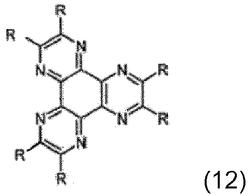
- The compound of formula 12 has a characteristic to be crystallized. Thus, by using the compound, the
hole injection layer 122 can have strength. The example of the compound of formula 12 includes HAT-CN (1,4,5,8,9,11-hexaazatriphenylene-hexacarbonitrile) of the following formula:
- The
hole injection layer 122 may be a single layer, or may be composed of two or more layers. In the latter case, one of the two or more layers may comprise the compound of formula 12. The thickness of thehole injection layer 122 may be in the range of from about 1 nm to about 1,000 nm, and preferably from about 5 nm to about 100 nm. Thehole injection layer 122 may be formed on thefirst electrode 110 by using known various methods such as vacuum deposition, wet film-forming methods, laser induced thermal imaging, etc. - The
hole transport layer 123 may be prepared with any hole transport material known in the art. Thehole transport layer 123 may be a single layer, or may be composed of two or more layers. The thickness of thehole transport layer 123 may be in the range of from about 1 nm to about 100 nm, and preferably from about 5 nm to about 80 nm. Thehole transport layer 123 may be formed on thehole injection layer 122 by using known various methods such as vacuum deposition, wet film-forming methods, laser induced thermal imaging, etc. - The light-emitting
layer 125 may be prepared with a host compound and a dopant compound. The host compound may be a phosphorescent host compound or a fluorescent host compound. The dopant compound may be a phosphorescent dopant compound or a fluorescent dopant compound. The kinds of host compound and dopant compound to be used are not particularly limited, and may be compounds having the aforementioned LUMO energy level and selected from compounds known in the art. Preferably, the host compound may be a fluorescent host compound. The fluorescent host compound may be an anthracene-based compound represented by the following formula 13.
- In formula 13, Ar1 and Ar2, each independently, may represent preferably, a substituted or unsubstituted (C6-C30)aryl. Specifically, Ar1 and Ar2, each independently, may represent a substituted or unsubstituted phenyl, a substituted or unsubstituted biphenyl, a substituted or unsubstituted naphthyl, a substituted or unsubstituted anthracenyl, a substituted or unsubstituted phenanthrenyl, a substituted or unsubstituted naphthacenyl, a substituted or unsubstituted fluoranthenyl, a substituted or unsubstituted pyrenyl, or a substituted or unsubstituted chrysenyl. In formula 13, Ar3 and Ar4, each independently, may represent preferably, hydrogen, a substituted or unsubstituted (C6-C21)aryl, a substituted or unsubstituted (5- to 21-membered) heteroaryl or -NR21R22.
- Specifically, the compound of formula 13 includes the following, but is not limited thereto:


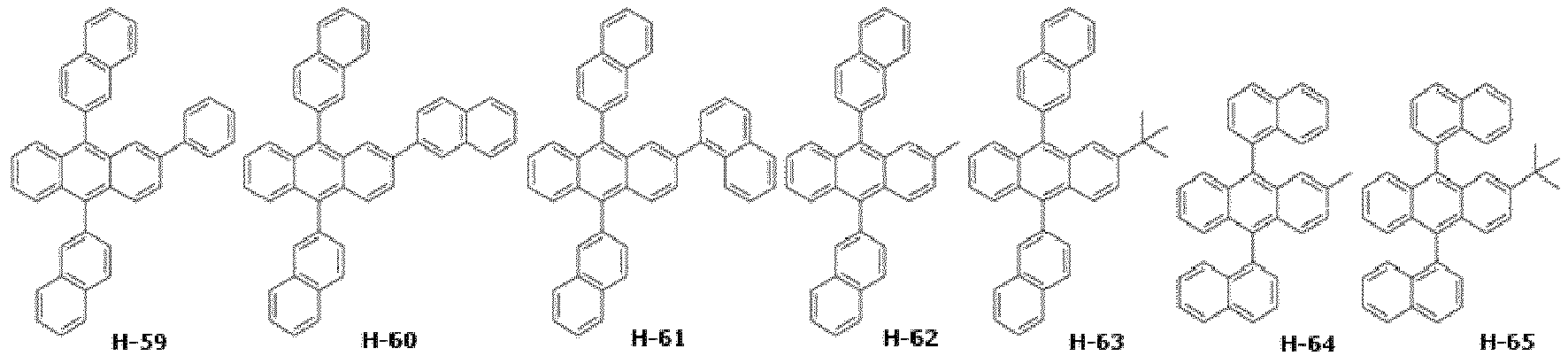



- Preferably, the dopant compound may be a fluorescent dopant compound. In view of light color required to be emitted, the fluorescent dopant compound may be selected preferably, from amine-based compounds, aromatic compounds, chelate complexes such as tris(8-quinolinolate)aluminum complexes, coumarine derivatives, tetraphenylbutadiene derivatives, bis-styrylarylene derivatives, oxadiazole derivatives, etc.; more preferably, styrylamine compounds, styryldiamine compounds, arylamine compounds, and aryldiamine compounds; and even more preferably, condensed polycyclic amide derivatives. The fluorescent dopant can be used solely or as a combination of two or more compounds.
- The fluorescent dopant compound may be a condensed polycyclic amine derivative represented by the following formula 14.


- A preferable aryl for Ar21 includes a substituted or unsubstituted phenyl, a substituted or unsubstituted fluorenyl, a substituted or unsubstituted anthryl, a substituted or unsubstituted pyrenyl, a substituted or unsubstituted chrysenyl, a substituted or unsubstituted benzofluorenyl, and spiro[fluoren-benzofluorene], etc.
- Specifically, the compound of formula 14 includes the following, but is not limited thereto:


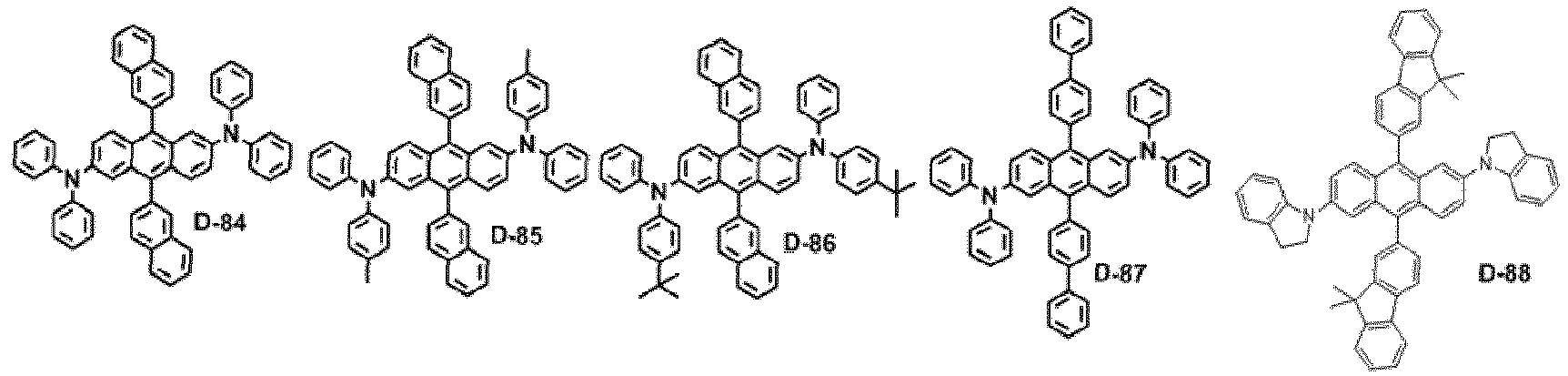


- When the light-emitting
layer 125 comprises a host and a dopant, the dopant can be doped in an amount of less than about 25 wt%, and preferably less than 17 wt%, based on the total amount of the dopant and host of the light-emitting layer. The thickness of the light-emittinglayer 125 can be in the range of from about 5 nm to about 100 nm, and preferably from about 10 nm to about 60 nm. Light emission occurs at the light-emittinglayer 125. The light-emittinglayer 125 may be a single layer, or may be composed of two or more layers. When thelight emitting layer 125 is composed of two or more layers, each of the layers may be prepared to emit color different from one another. For example, the device may emit white light by preparing three light-emittinglayers 125 which emit blue, red, and green, respectively. The light-emittinglayer 125 may be formed on thehole transport layer 123 by using known various methods such as vacuum deposition, wet film-forming methods, laser induced thermal imaging, etc. - The
electron buffering layer 126 employs the compound offormula 1 of the present disclosure. The details of the compound offormula 1 are as previously described. The thickness of theelectron buffering layer 126 is 1 nm or more, but is not particularly limited thereto. Specifically, the thickness of theelectron buffering layer 126 may be in the range of from 2 nm to 200 nm. Theelectron buffering layer 126 may be formed on the light-emittinglayer 125 by using known various methods such as vacuum deposition, wet film-forming methods, laser induced thermal imaging, etc. - The
electron transport layer 127 may be prepared with any electron transport material known in the art, which includes oxazole-based compounds, isoxazole-based compounds, triazole-based compounds, isothiazole-based compounds, oxadiazole-based compounds, thiadiazole-based compounds, perylene-based compounds, anthracene-based compounds, aluminum complexes, and gallium complexes, but is not limited thereto. The anthracene-based compound may be a compound represented by the following formula 15.
- In formula 15, preferably, one of R31 to R35 may be a substituted or unsubstituted (C6-C18)aryl, or a substituted or unsubstituted (5- to 18-membered)heteroaryl, the rest of R31 to R35 may be hydrogen; Q2 and Q7, each independently, may represent a substituted or unsubstituted (C6-C30)aryl or a substituted or unsubstituted (3- to 30-membered)heteroaryl; Q1, Q3 to Q6, Q8, and Q9 may represent hydrogen; and k may represent 1.
- The specific compound of formula 15 includes the following compound:
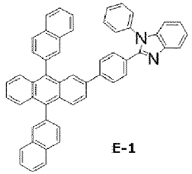
- Preferably, the
electron transport layer 127 may be a mixed layer comprising an electron transport compound and a reductive dopant. In this case, the electron transport compound is reduced to an anion, and thus it becomes easier to inject and transport electrons to an electroluminescent medium. The electron transport compound for the mixed layer is not particularly limited, and may be any of the aforementioned known electron transport materials. The reductve dopant may be selected from alkali metals, alkali metal compounds, alkaline earth metals, rare-earth metals, and halides, oxides, and complexes thereof. Specifically, the reductive dopant includes lithium quinolate, sodium quinolate, cesium quinolate, potassium quinolate, LiF, NaCl, CsF, Li2O, BaO, and BaF2, but are not limited thereto. The thickness of theelectron transport layer 127 may be in the range of from about 5 to about 100 nm, and preferably from about 10 to about 60 nm. Theelectron transport layer 127 may be formed on theelectron buffering layer 126 by using known various methods such as vacuum deposition, wet film-forming methods, laser induced thermal imaging, etc. - The
electron injection layer 128 may be prepared with any electron injection material known in the art, which includes lithium quinolate, sodium quinolate, cesium quinolate, potassium quinolate, LiF, NaCl, CsF, Li2O, BaO, and BaF2, but is not limited thereto. The thickness of the electron injection layer may be in the range of from about 0.1 to about 10 nm, and preferably from about 0.3 to about 9 nm. Theelectron injection layer 128 may be formed on the electron transport layer by using known various methods such as vacuum deposition, wet film-forming methods, laser induced thermal imaging, etc. - The
second electrode 130 may be a cathode, and may be prepared with a low work-function material. The material for thesecond electrode 130 includes aluminum (Al), calcium (Ca), magnesium (Mg), silver (Ag), cesium (Cs), lithium (Li), and a combination thereof. Thesecond electrode 130 may be formed by any method known in the art, such as vacuum deposition, sputtering, etc. - The aforementioned description regarding the organic electroluminescent device shown in
Figure 1 is intended to explain one embodiment of the invention, and is not meant in any way to restrict the scope of the invention. The organic electroluminescent device can be constructed in another way. For example, any one optional component such as a hole injection layer may not be comprised in the organic electroluminescent device ofFigure 1 , except for a light-emitting layer and an electron buffering layer. In addition, an optional component may be further comprised therein, which includes an impurity layer such as n-doping layer and p-doping layer. The organic electroluminescent device may be a both side emission type in which a light-emitting layer is placed on each of both sides of the impurity layer. The two light-emitting layers on the impurity layer may emit different colors. The organic electroluminescent device may be a bottom emission type in which a first electrode is a transparent electrode and a second electrode is a reflective electrode. The organic electroluminescent device may be a top emission type in which a first electrode is a reflective electrode and a second electrode is a transparent electrode. The organic electroluminescent device may have an inverted type structure in which a cathode, an electron transport layer, a light-emitting layer, a hole transport layer, a hole injection layer, and an anode are sequentially stacked on a substrate. -
Figure 2 illustrates an energy band diagram among a hole transport layer, a light-emitting layer, an electron buffering layer, and an electron transport zone of an organic electroluminescent device according to one embodiment of the present disclosure. - In
Figure 2 , ahole transport layer 123, a light-emittinglayer 125, anelectron buffering layer 126, and anelectron transport zone 129 are sequentially stacked. Electrons (e) injected from a cathode are transported to a light-emitting layer through anelectron transport zone 129 and anelectron buffering layer 126. LUMO energy level of anelectron buffering layer 126 may be higher than those of a host compound and a dopant compound of a light-emittinglayer 125, and anelectron transport layer 127. Specifically, LUMO energy levels may have the following relationship: the electron buffering layer > the electron transport zone > the host compound. According to prior arts, light-emitting sites in a light-emitting layer are shifted to a hole transport layer due to hole trap, thereby light being emitted at an interface. However, according to the present disclosure, electrons(e) are trapped due to the aforementioned LUMO energy level of anelectron buffering layer 126, so that light-emitting sites in a light-emitting layer can be shifted to anelectron transport zone 129, and thus lifespan and efficiencies of an organic electroluminescent device can be improved. Meanwhile, HOMO energy level of anelectron buffering layer 126 is higher than those of a host compound and a dopant compound of a light-emittinglayer 125, but may be lower or higher than HOMO energy level of anelectron transport zone 129. - Hereinafter, a preparation method of an organic electroluminescent device according to one embodiment of the present disclosure, and luminescent properties of the device will be explained in detail with reference to the following examples.
- OLED was produced as follows. A transparent electrode indium tin oxide (ITO) thin film (15 Ω/sq) on a glass substrate for an OLED (Samsung Corning) was subjected to an ultrasonic washing with trichloroethylene, acetone, ethanol, and distilled water, sequentially, and then was stored in isopropanol. The ITO substrate was then mounted on a substrate holder of a vacuum vapor depositing apparatus. N4,N4'-diphenyl-N4,N4'-bis(9-phenyl-9H-carbazol-3-yl)-[1,1'-biphenyl]-4,4'-diamine was introduced into a cell of the vacuum vapor depositing apparatus, and then the pressure in the chamber of said apparatus was controlled to 10-6 torr. Thereafter, an electric current was applied to the cell to evaporate the above introduced material, thereby forming a first hole injection layer having a thickness of 60 nm on the ITO substrate. 1,4,5,8,9,11-hexaazetriphenylene-hexacarbonitrile (HAT-CN) was then introduced into another cell of the vacuum vapor depositing apparatus, and was evaporated by applying an electric current to the cell, thereby forming a second hole injection layer having a thickness of 5 nm on the first hole injection layer. N-([1,1'-biphenyl]-4-yl)-9,9-dimethyl-N-(4-(9-phenyl-9H-carbazol-3-yl)phenyl)-9H-fluoren-2-amine (HT-1) was then introduced into another cell of the vacuum vapor depositing apparatus, and was evaporated by applying an electric current to the cell, thereby forming a first hole transport layer having a thickness of 20 nm on the second hole injection layer. Thereafter, HT-2 was introduced into another cell of the vacuum vapor depositing apparatus, and was evaporated by applying an electric current to the cell, thereby forming a second hole transport layer having a thickness of 5 nm on the first hole transport layer. Thereafter, compound H-1 was introduced into one cell of the vacuum vapor depositing apparatus, as a host material, and compound D-38 was introduced into another cell as a dopant. The two materials were evaporated at different rates, so that the dopant was deposited in a doping amount of 2 wt% based on the total amount of the host and dopant to form a light-emitting layer having a thickness of 20 nm on the hole transport layer. 2-(4-(9,10-di(naphthalen-2-yl)anthracen-2-yl)phenyl)-1-phenyl-1H-benzo[d]imidazole was then introduced into one cell, and lithium quinolate was introduced into another cell. The two materials were evaporated at the same rate, so that they were respectively deposited in a doping amount of 50 wt% to form an electron transport layer having a thickness of 35 nm on the light-emitting layer. After depositing lithium quinolate as an electron injection layer having a thickness of 2 nm on the electron transport layer, an Al cathode having a thickness of 80 nm was then deposited by another vacuum vapor deposition apparatus on the electron injection layer. Thus, an OLED was produced. All the material used for producing the OLED device were those purified by vacuum sublimation at 10-6 torr.
-
Figure 3 shows a graph illustrating a current efficiency versus a luminance of the prepared organic electroluminescent device. In addition, luminous efficiency, CIE color coordinate, a driving voltage at 1,000 nit of luminance, and a lifespan for 10 hours at 2,000 nit and a constant current are shown in Table 1 below. - OLEDs were produced and evaluated in the same manner as in Comparative Example 1, except that a thickness of an electron transport layer was 30 nm, and an electron buffering layer having a thickness of 5 nm was interposed between a light-emitting layer and an electron transport layer. Electron buffering materials used in Examples 1 to 3 are shown in Tables 1 and 4 below.
Figure 3 shows a graph illustrating a current efficiency versus a luminance of the prepared organic electroluminescent device. In addition, evaluation results of the devices prepared in Examples 1 to 3 are shown in Table 1 below. - OLEDs were produced and evaluated in the same manner as in Example 1, except that BF-1 and BF-65 were used for an electron buffering material and HT-3 was used for a second hole transport layer. Evaluation results of the devices prepared in Comparative Examples 2 and 3 were shown in Table 1 below.
[Table 1] Second Hole Transport Layer Electron Buffering Material Voltage (V) Current Efficiency (cd/A) Color coordinate (x) Color coordinate (y) Lifespan (hr) LUMO (eV) HOMO (eV) Comparative Ex. 1 HT-2 - 4.2 6.3 0.140 0.097 95.6 Comparative Ex. 2 HT-3 BF-1 4.5 6.6 0.140 0.095 95.4 1.95 5.48 Comparative Ex. 3 HT-3 BF-65 4.4 6.8 0.140 0.098 95.8 1.92 5.55 Example 1 HT-2 B-34 4.3 7.2 0.140 0.095 95.6 1.96 5.33 Example 2 HT-2 B-57 4.1 7.6 0.139 0.097 96.4 1.94 5.34 Example 3 HT-2 B-90 4.1 7.6 0.139 0.098 95.7 1.97 5.32 - From Table 1 above, it is recognized that due to speediness of electron current by the electron buffering material of the present disclosure, the devices of Examples 1 to 3 show higher efficiencies and longer lifespan than those of Comparative Examples 1 to 3 in which an electron buffering layer is not comprised or an electron buffering material of the present disclosure is not used to prepare an electron buffering layer. LUMO energy levels of the electron buffering layer of Examples 1 to 3 were about 1.9 eV; LUMO energy level of the host compound was about 1.6 eV; and LUMO energy level of the electron transport layerwas about 1.8 eV. From
Figure 3 , it is recognized that the organic electroluminescent devices of Examples 1 to 3 show higher current efficiencies over the whole range of luminance than the organic electroluminescent device of Comparative Example 1. - OLEDs were produced in the same manner as in Comparative Example 1, except that a compound for a second hole transport layer was changed to HT-3 shown in Table 4 below. Luminous efficiency, CIE color coordinate, a driving voltage at 1,000 nit of luminance, and time taken for luminance to be reduced from 100% to 90% at 2,000 nit and a constant current are shown in Table 2 below.
- OLEDs were produced and evaluated in the same manner as in Comparative Example 4, except that a thickness of an electron transport layer was 30 nm, and an electron buffering layer having a thickness of 5 nm and comprising an electron buffering material was interposed between a light-emitting layer and an electron transport layer. Electron buffering materials used in Examples 4 to 8 are shown in Tables 2 and 4 below. Evaluation results of the devices prepared in Examples 4 to 8 are shown in Table 2 below.
[Table 2] Second Hole Transport Layer Electron Buffering Material Voltage (V) Current Efficiency (cd/A) Color coordinate (x) Color coordinate (y) Lifespan (hr) LUMO (eV) HOMO (eV) Comparative Ex. 4 HT-3 - 4.1 6.5 0.139 0.094 27.9 Example 4 HT-3 B-143 4.3 6.6 0.139 0.095 37.0 1.95 5.21 Example 5 HT-3 B-145 4.4 6.9 0.139 0.096 47.3 1.90 5.43 Example 6 HT-3 B-144 4.3 6.9 0.139 0.098 39.7 1.97 5.15 Example 7 HT-3 B-147 4.3 6.8 0.139 0.095 35.1 1.89 5.40 Example 8 HT-3 B-149 4.2 7.2 0.139 0.097 34.8 1.88 5.43 - It is recognized that due to speediness of electron current by the electron buffering material of the present disclosure, the devices of Examples 4 to 8 have similar current characteristics to one of Comparative Example 4, but show higher efficiencies and longer lifespan than those of Comparative Example 4.
- OLEDs were produced and evaluated in the same manner as in Comparative Example 1, except that a thickness of a first hole transport layer was 10 nm; HT-4 was used to form a second hole transport layer having a thickness of 30 nm on a first hole transport layer; and H-44 and D-88 were used as a host and a dopant, respectively. The prepared OLED was evaluated as to luminous efficiency, CIE color coordinate, a driving voltage at 1,000 nit of luminance, and time taken for luminance to be reduced from 100% to 90% at 2,000 nit and a constant current, and the results are shown in Table 3 below.
- OLEDs were produced and evaluated in the same manner as in Comparative Example 5, except that a thickness of an electron transport layer was 30 nm, and an electron buffering layer having a thickness of 5 nm and comprising an electron buffering material was interposed between a light-emitting layer and an electron transport layer. Electron buffering materials used in Examples 9 and 10 are shown in Table 3 below, along with evaluation results of the prepared devices.
[Table 3] Second Hole Transport Layer Electron Buffering Material Voltage (V) Current Efficiency (cd/A) Color coordinate (x) Color coordinate (y) Lifespan (hr) LUMO (eV) HOMO (eV) Comparative Ex. 5 HT-4 - 3.4 28.9 0.291 0.677 25.0 Example 9 HT-4 B-57 3.4 30.7 0.291 0.677 25.0 1.94 5.34 Example 10 HT-4 B-145 3.4 30.3 0.291 0.676 27.0 1.90 5.43 - It is recognized that due to speediness of electron current by the electron buffering material of the present disclosure, the devices of Examples 9 to 10 have similar current characteristics to one of Comparative Example 5 in which an electron buffering layer is not comprised, but show higher efficiencies and longer lifespan than those of Comparative Example 5.
[Table 4] Compounds for a hole transport layer of the Comparative Examples and the Examples Hole Transport Layer 
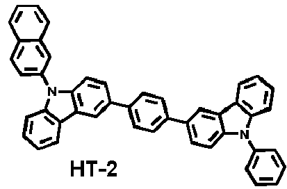


- OLEDs were produced in the same manner as in Example 1, except that compounds shown in Table 5 below were used as an electron buffering material. The electron buffering layer was formed by a co-evaporation of the two compounds shown in Table 5. The prepared OLEDs were evaluated as to luminous efficiency, CIE color coordinate, a driving voltage at 1,000 nit of luminance, and lifespan for 10 hours at 2,000 nit and a constant current, and the results are shown in Table 5 below.
[Table 5] Hole Injection Layer Electron buffering material (mixing ratio = 5:5) Voltage (V) Current Efficiency (cd/A) Color coordinate (x) Color coordinate (y) Lifespan (10hr) (%) Example 11 HT-2 BF-3:B-57 4.4 7.1 0.139 0.095 96.2 Example 12 HT-2 BF-4:B-57 4.2 7.3 0.139 0.094 95.9 Example 13 HT-2 BF-5:B-57 4.3 7.2 0.139 0.095 96.3 Example 14 HT-2 BF-3:B-145 4.4 7.2 0.139 0.097 96.5 Example 15 HT-2 BF-4:B-145 4.3 7.3 0.139 0.098 96.5 Example 16 HT-2 BF-5:B-145 4.4 7.1 0.139 0.095 96.5 - From Table 5 above, it is recognized that due to speediness of electron current by the electron buffering material of the present disclosure, the devices of Examples 11 to 16 show higher efficiency and longer lifespan than those of Comparative Examples 1 to 3 shown in Table 1 in which an electron buffering layer was not comprised or an electron buffering material of the present disclosure is not used to prepare an electro buffer layer.
- OLEDs were produced in the same manner as in Example 1, except that compounds shown in Table 6 below were used as an electron buffering material. The electron buffering layer of Example 17 was formed by a co-evaporation, while the electron buffering layer of Example 18 was formed by a mixture-evaporation. The prepared OLEDs were evaluated as to luminous efficiency, CIE color coordinate, a driving voltage at 1,000 nit of luminance, and lifespan for 10 hours at 2,000 nit and a constant current, and the results are shown in Table 6 below.
[Table 6] Hole Injection Layer Electron buffering material (mixing ratio = 5:5) Voltage (V) Current Efficiency (cd/A) Color coordinate (x) Color coordinate (y) Lifespan (10hr) (%) Example 17 HT-2 B-145:BF-6 4.5 6.7 0.139 0.095 97.4 Example 18 HT-2 B-145:BF-6 4.5 6.7 0.139 0.095 97.4 - From Table 6 above, it is recognized that due to speediness of electron current by the electron buffering material of the present disclosure, the devices of Examples 17 and 18 show higher efficiency than those of Comparative Examples 1 to 3 shown in Table 1 in which an electron buffering layer was not comprised or an electron buffering material of the present disclosure is not used to prepare an electro buffer layer. In particular, lifespan was significantly enhanced by 97.4%. Furthermore, B-145 and BF-6 have the same deposition temperature, and thus are suitable for a mixture-evaporation. Example 18 shows that an electron buffering layer can be formed by a mixture-evaporation with the material. A respective deposition temperature of the compounds in a vacuum vapor depositing apparatus are shown in Table 7 below. The mixture-evaporation method for an electron buffering layer has an advantage in that device characteristics can be maintained until the whole material is consumed in a crucible.
[Table 7] Electron buffering compound Deposition Temperature (°C) (0.5 Å/s at 10-7 torr) B-145 245 BF-6 244 Description of Reference Numerals 100: organic electroluminescent device 101: substrate 110: first electrode 120: organic layer 122: hole injection layer 123: hole transport layer 125: light-emitting layer 126: electron buffering layer 127: electron transport layer 128: electron injection layer 129: electron transport zone 130: second electrode
Claims (9)
- An electron buffering material comprising a compound represented by the following formula 1:
 A represents a substituted or unsubstituted (5- to 30-membered)heteroaryl;L represents a single bond, a substituted or unsubstituted (C6-C30)arylene, or a substituted or unsubstituted (5- to 30-membered)heteroarylene;R1 represents the following formula 2a:
 R2 represents hydrogen, deuterium, a halogen, a cyano, a substituted or unsubstituted (C1-C30)alkyl, a substituted or unsubstituted (C6-C30)aryl, a substituted or unsubstituted (5-to 30-membered)heteroaryl, a substituted or unsubstituted (C3-C30)cycloalkyl, a substituted or unsubstituted (C1-C30)alkoxy, a substituted or unsubstituted tri(C1-C30)alkylsilyl, a substituted or unsubstituted tri(C6-C30)arylsilyl, a substituted or unsubstituted di(C1-C30)alkyl(C6-C30)arylsilyl, a substituted or unsubstituted (C1-C30)alkyldi(C6-C30)arylsilyl, a substituted or unsubstituted mono- or di-(C1-C30)alkylamino, a substituted or unsubstituted mono- or di-(C6-C30)arylamino, a substituted or unsubstituted (C1-C30)alkyl(C6-C30)arylamino, or the following formula 3; or may be fused with the carbazole backbone to form a substituted or unsubstituted benzocarbazole;
 X represents O, S, CR11R12, NR13 or SiR13R14;R3 represents hydrogen, deuterium, a halogen, a cyano, a substituted or unsubstituted (C1-C30)alkyl, a substituted or unsubstituted (C6-C30)aryl, a substituted or unsubstituted (5-to 30-membered)heteroaryl, a substituted or unsubstituted (C3-C30)cycloalkyl, a substituted or unsubstituted (C1-C30)alkoxy, a substituted or unsubstituted tri(C1-C30)alkylsilyl, a substituted or unsubstituted tri(C6-C30)arylsilyl, a substituted or unsubstituted di(C1-C30)alkyl(C6-C30)arylsilyl, a substituted or unsubstituted (C1-C30)alkyldi(C6-C30)arylsilyl, a substituted or unsubstituted mono- or di-(C1-C30)alkylamino, a substituted or unsubstituted mono- or di-(C6-C30)arylamino, or a substituted or unsubstituted (C1-C30)alkyl(C6-C30)arylamino;R4, R5 and R10, each independently, represent hydrogen, deuterium, a halogen, a cyano, a substituted or unsubstituted (C1-C30)alkyl, a substituted or unsubstituted (C6-C30)aryl, a substituted or unsubstituted (5- to 30-membered)heteroaryl, a substituted or unsubstituted (C3-C30)cycloalkyl, a substituted or unsubstituted (C1-C30)alkoxy, a substituted or unsubstituted tri(C1-C30)alkylsilyl, a substituted or unsubstituted tri(C6-C30)arylsilyl, a substituted or unsubstituted di(C1-C30)alkyl(C6-C30)arylsilyl, a substituted or unsubstituted (C1-C30)alkyldi(C6-C30)arylsilyl, a substituted or unsubstituted mono- or di-(C1-C30)alkylamino, a substituted or unsubstituted mono- or di-(C6-C30)arylamino, or a substituted or unsubstituted (C1-C30)alkyl(C6-C30)arylamino; or may be linked to an adjacent substituent(s) to form a substituted or unsubstituted (C3-C30), mono- or polycyclic, alicyclic or aromatic ring whose carbon atom(s) may be replaced with at least one hetero atom selected from nitrogen, oxygen, and sulfur;R6 represents a substituted or unsubstituted (C1-C30)alkyl, a substituted or unsubstituted (C6-C30)aryl, a substituted or unsubstituted (5- to 30-membered)heteroaryl, a substituted or unsubstituted (C3-C30)cycloalkyl, a substituted or unsubstituted mono- or di-(C1-C30)alkylamino, a substituted or unsubstituted mono- or di-(C6-C30)arylamino, or a substituted or unsubstituted (C1-C30)alkyl(C6-C30)arylamino;R11 to R14, each independently, represent a substituted or unsubstituted (C1-C30)alkyl, a substituted or unsubstituted (C6-C30)aryl, or a substituted or unsubstituted (5- to 30-membered)heteroaryl; or may be linked to an adjacent substituent(s) to form a substituted or unsubstituted (C3-C30), mono- or polycyclic, alicyclic or aromatic ring whose carbon atom(s) may be replaced with at least one hetero atom selected from nitrogen, oxygen, and sulfur;a, c, d and f, each independently, represent an integer of 0 to 4; where a, c, d or f is an integer of 2 or more, each of R2, R4, R5 or R10 may be the same or different;b represents an integer of 0 to 3; where b is an integer of 2 or more, each of R3 may be the same or different;n represents an integer of 0 or 1; m represents an integer of 1 or 2;* represents a bonding site to the carbazole backbone; andthe heteroaryl(ene) contains one or more hetero atoms selected from B, N, O, S, P(=O), Si, and P;wherein the substituents of the substituted (C1-C30)alkyl, the substituted (C1-C30)alkoxy, the substituted (C3-C30)cycloalkyl, the substituted (C6-C30)aryl(ene), the substituted (5- to 30-membered)heteroaryl(ene) and the substituted (C6-C30)aryl(C1-C30)alkyl in A, L, R2 to R6 and R10 to R14 of formula 1 of the present disclosure, each independently, are at least one selected from the group consisting of deuterium, a halogen, a cyano, a carboxy, a nitro, a hydroxy, a (C1-C30)alkyl, a halo(C1-C30)alkyl, a (C2-C30)alkenyl, a (C2-C30)alkynyl, a (C1-C30)alkoxy, a (C1-C30)alkylthio, a (C3-C30)cycloalkyl, a (C3-C30)cycloalkenyl, a (3- to 7-membered)heterocycloalkyl, a (C6-C30)aryloxy, a (C6-C30)arylthio, a (3- to 30-membered)heteroaryl unsubstituted or substituted with a (C6-C30)aryl, a (C6-C30)aryl unsubstituted or substituted with a (3- to 30-membered)heteroaryl, a tri(C1-C30)alkylsilyl, a tri(C6-C30)arylsilyl, a di(C1-C30)alkyl(C6-C30)arylsilyl, a (C1-C30)alkyldi(C6-C30)arylsilyl, an amino, a mono- or di-(C1-C30)alkylamino, a mono- or di-(C6-C30)arylamino, a (C1-C30)alkyl(C6-C30)arylamino, a (C1-C30)alkylcarbonyl, a (C1-C30)alkoxycarbonyl, a (C6-C30)arylcarbonyl, a di(C6-C30)arylboronyl, a di(C1-C30)alkylboronyl, a (C1-C30)alkyl(C6-C30)arylboronyl, a (C6-C30)aryl(C1-C30)alkyl, and a (C1-C30)alkyl(C6-C30)aryl.
 - The electron buffering material according to claim 1, wherein A represents a substituted or unsubstituted nitrogen-containing (5- to 30-membered)heteroaryl; L represents a single bond or a substituted or unsubstituted (C6-C20)arylene; R1 represents formula 2a; R2 represents hydrogen, deuterium, a substituted or unsubstituted (C6-C20)aryl, a substituted or unsubstituted (5- to 20-membered)heteroaryl, a substituted or unsubstituted mono- or di-(C6-C20)arylamino or formula 3, or may be fused with the carbazole backbone to form a substituted or unsubstituted benzocarbazole; X represents O, S, CR11R12, or NR13; R10 represents hydrogen or (C1-C20)alkyl; R3, R4 and R5, each independently, represent hydrogen or a substituted or unsubstituted (C1-C20)alkyl; R6 represents a substituted or unsubstituted (C1-C20)alkyl, a substituted or unsubstituted (C6-C20)aryl, or a substituted or unsubstituted (6- to 20-membered)heteroaryl; R11 to R14, each independently, represent hydrogen, a substituted or unsubstituted (C1-C10)alkyl, a substituted or unsubstituted (C6-C20)aryl, or a substituted or unsubstituted (5- to 20-membered)heteroaryl; and the heteroaryl contains one or more hetero atoms selected from N, O and S.
- The electron buffering material according to claim 1, wherein the compound of formula 1 is selected from the group consisting of:











- The electron buffering material according to claim 1, wherein a compound represented by the following formula 11 is further comprised:
 Ar5 and Ar6, each independently, represent a substituted or unsubstituted (5- to 30-membered)heteroaryl, or a substituted or unsubstituted (C6-C30)aryl;L' represents a single bond, a substituted or unsubstituted (C6-C30)arylene, or a substituted or unsubstituted (3- to 30-membered)heteroarylene;X1 to X3, each independently, represent N or C, with the proviso that at least one of X1 to X3 represents N;R15 and R16, each independently, represent hydrogen, deuterium, a halogen, a cyano, a carboxy, a nitro, a hydroxy, a substituted or unsubstituted (C1-C30)alkyl, a substituted or unsubstituted (C6-C30)aryl, a substituted or unsubstituted (5- to 30-membered)heteroaryl, a substituted or unsubstituted (C3-C30)cycloalkyl, a substituted or unsubstituted (C3-C30)cycloalkenyl, a substituted or unsubstituted (3- to 7-membered)heterocycloalkyl, a substituted or unsubstituted (C1-C30)alkoxy, a substituted or unsubstituted tri(C1-C30)alkylsilyl, a substituted or unsubstituted tri(C6-C30)arylsilyl, a substituted or unsubstituted di(C1-C30)alkyl(C6-C30)arylsilyl, a substituted or unsubstituted (C1-C30)alkyldi(C6-C30)arylsilyl, a substituted or unsubstituted mono- or di-(C1-C30)alkylamino, a substituted or unsubstituted mono- or di-(C6-C30)arylamino, or a substituted or unsubstituted (C1-C30)alkyl(C6-C30)arylamino; or may be linked to an adjacent substituent(s) to form a substituted or unsubstituted (C3-C30), mono- or polycyclic, alicyclic or aromatic ring whose carbon atom(s) may be replaced with at least one hetero atom selected from nitrogen, oxygen, and sulfur;the heteroaryl(ene) and heterocycloalkyl, each independently, contain one or more hetero atoms selected from B, N, O, S, P(=O), Si and P; ands and t, each independently, represent an integer of 1 to 4; where s or t is an integer of 2 or more, each of R15 or R16 may be the same or different.
 - The electron buffering material according to claim 4, wherein Ar5 and Ar6, each independently, represent a substituted or unsubstituted (6- to 20-membered)heteroaryl, or a substituted or unsubstituted (C6-C20)aryl; L' represents a single bond, or a substituted or unsubstituted (C6-C20)arylene; R15 and R16, each independently, represent hydrogen, a substituted or unsubstituted (C6-C20)aryl, or a substituted or unsubstituted (5- to 20-membered)heteroaryl, or may be linked to an adjacent substituent(s) to form a substituted or unsubstituted (C5-C20), mono- or polycyclic aromatic ring whose carbon atom(s) may be replaced with at least one hetero atom selected from nitrogen, oxygen, and sulfur; and s and t represent 1.
- The electron buffering material according to claim 4, wherein the compound of formula 11 is selected from the group consisting of:


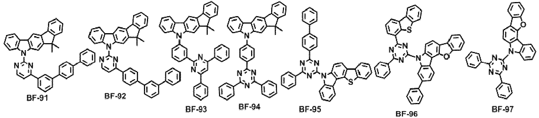
- An organic electroluminescent device comprising a first electrode, a second electrode facing the first electrode, a light-emitting layer between the first electrode and the second electrode, and an electron transport zone and an electron buffering layer between the light-emitting layer and the second electrode, wherein the electron buffering layer comprises the compound represented by formula 1 according to claim 1.
- The organic electroluminescent device according to claim 7, wherein the electron buffering layer further comprises the compound represented by formula 11 according to claim
- The organic electroluminescent device according to claim 8, wherein the compound represented by formula 1 and the compound represented by formula 11 of the electron buffering layer are co-evaporated or mixture-evaporated.
Applications Claiming Priority (4)
| Application Number | Priority Date | Filing Date | Title |
|---|---|---|---|
| KR20140031295 | 2014-03-17 | ||
| KR1020150036207A KR102411748B1 (en) | 2014-03-17 | 2015-03-16 | Electron Buffering Material and Organic Electroluminescent Device |
| EP15764804.9A EP3119751B1 (en) | 2014-03-17 | 2015-03-17 | Electron buffering material and organic electroluminescent device |
| PCT/KR2015/002592 WO2015142040A1 (en) | 2014-03-17 | 2015-03-17 | Electron buffering material and organic electroluminescent device |
Related Parent Applications (2)
| Application Number | Title | Priority Date | Filing Date |
|---|---|---|---|
| EP15764804.9A Division EP3119751B1 (en) | 2014-03-17 | 2015-03-17 | Electron buffering material and organic electroluminescent device |
| EP15764804.9A Division-Into EP3119751B1 (en) | 2014-03-17 | 2015-03-17 | Electron buffering material and organic electroluminescent device |
Publications (2)
| Publication Number | Publication Date |
|---|---|
| EP3415508A1 true EP3415508A1 (en) | 2018-12-19 |
| EP3415508B1 EP3415508B1 (en) | 2021-04-21 |
Family
ID=54246383
Family Applications (2)
| Application Number | Title | Priority Date | Filing Date |
|---|---|---|---|
| EP18180522.7A Active EP3415508B1 (en) | 2014-03-17 | 2015-03-17 | Electron buffering material and organic electroluminescent device |
| EP15764804.9A Active EP3119751B1 (en) | 2014-03-17 | 2015-03-17 | Electron buffering material and organic electroluminescent device |
Family Applications After (1)
| Application Number | Title | Priority Date | Filing Date |
|---|---|---|---|
| EP15764804.9A Active EP3119751B1 (en) | 2014-03-17 | 2015-03-17 | Electron buffering material and organic electroluminescent device |
Country Status (5)
| Country | Link |
|---|---|
| US (1) | US20170005276A1 (en) |
| EP (2) | EP3415508B1 (en) |
| JP (1) | JP6741584B2 (en) |
| KR (1) | KR102411748B1 (en) |
| CN (1) | CN106068261B (en) |
Families Citing this family (36)
| Publication number | Priority date | Publication date | Assignee | Title |
|---|---|---|---|---|
| KR20150108330A (en) * | 2014-03-17 | 2015-09-25 | 롬엔드하스전자재료코리아유한회사 | Electron buffering material and organic electroluminescent device comprising the same |
| KR101537499B1 (en) * | 2014-04-04 | 2015-07-16 | 주식회사 엘지화학 | Organic light emitting diode |
| KR102427918B1 (en) * | 2014-04-29 | 2022-08-03 | 롬엔드하스전자재료코리아유한회사 | Electron transport material and an organic electroluminescence device comprising the same |
| KR102457008B1 (en) * | 2014-05-23 | 2022-10-19 | 가부시키가이샤 한도오따이 에네루기 켄큐쇼 | Heterocyclic compound, light-emitting element, light-emitting device, electronic device, and lighting device |
| WO2016018076A1 (en) * | 2014-07-29 | 2016-02-04 | Rohm And Haas Electronic Materials Korea Ltd. | Electron buffering material and organic electroluminescent device |
| KR20160029187A (en) * | 2014-09-04 | 2016-03-15 | 삼성디스플레이 주식회사 | Organic light emitting diode and organic light emitting display device including the same |
| KR102369595B1 (en) * | 2014-12-08 | 2022-03-04 | 삼성디스플레이 주식회사 | Organic light emitting device and display device having the same |
| EP3316328A4 (en) * | 2015-06-23 | 2019-02-27 | Kaneka Corporation | ORGANIC ELECTROLUMINESCENT MATERIAL AND ORGANIC ELECTROLUMINESCENT ELEMENT USING THE SAME |
| KR102494453B1 (en) * | 2015-10-05 | 2023-02-02 | 삼성디스플레이 주식회사 | Organic electroluminescent device and display device including the same |
| KR101957788B1 (en) * | 2016-02-25 | 2019-03-13 | 주식회사 엘지화학 | Heterocyclic compound and organic light emitting device comprising the same |
| CN118772139A (en) * | 2016-03-15 | 2024-10-15 | 陶氏环球技术有限责任公司 | Organic electroluminescent compound and organic electroluminescent device thereof |
| KR102027030B1 (en) * | 2016-05-27 | 2019-09-30 | 주식회사 엘지화학 | Organic light emitting device |
| US10496720B2 (en) * | 2016-08-04 | 2019-12-03 | Facebook, Inc. | Systems and methods for providing feed preference surveys in a social networking system |
| KR102455656B1 (en) | 2016-09-22 | 2022-10-19 | 롬엔드하스전자재료코리아유한회사 | Organic Electroluminescent Device Comprising an Electron Buffer Layer and an Electron Transport Layer |
| KR102731722B1 (en) * | 2016-09-29 | 2024-11-20 | 듀폰스페셜티머터리얼스코리아 유한회사 | Organic electroluminescent device comprising electron transport layer and electron buffer layer |
| US10153445B2 (en) * | 2016-11-21 | 2018-12-11 | Universal Display Corporation | Organic electroluminescent materials and devices |
| WO2018095389A1 (en) * | 2016-11-23 | 2018-05-31 | 广州华睿光电材料有限公司 | Nitrogen-containing fused heterocyclic ring compound and application thereof |
| JP6893020B2 (en) * | 2017-04-05 | 2021-06-23 | 株式会社Joled | Manufacturing method of organic EL display panel and organic EL display panel |
| KR101985588B1 (en) * | 2017-06-21 | 2019-06-03 | 성균관대학교산학협력단 | Delayed fluorescence material and organic light emitting device having the delayed fluorescence material as a host material or a dopant material in light emitting layer of the organic light emitting device |
| KR102121433B1 (en) | 2017-09-01 | 2020-06-10 | 주식회사 엘지화학 | Novel compound and organic light emitting device comprising the same |
| CN110799510B (en) * | 2017-11-17 | 2023-07-14 | 株式会社Lg化学 | Compound and organic light-emitting device containing same |
| CN110272427B (en) * | 2018-03-14 | 2022-03-29 | 江苏三月科技股份有限公司 | Compound with fluorene as core, preparation method thereof and application thereof in organic electroluminescent device |
| KR102508374B1 (en) * | 2018-04-17 | 2023-03-10 | 엘티소재주식회사 | Heterocyclic compound and organic light emitting device comprising the same |
| WO2020050624A1 (en) * | 2018-09-04 | 2020-03-12 | 주식회사 엘지화학 | Polycyclic compound and organic light emitting diode comprising same |
| US11485706B2 (en) * | 2018-09-11 | 2022-11-01 | Universal Display Corporation | Organic electroluminescent materials and devices |
| US20210013437A1 (en) * | 2018-09-29 | 2021-01-14 | Tcl Technology Group Corporation | Quantum dot light-emitting diode |
| KR102213664B1 (en) | 2018-11-28 | 2021-02-05 | 삼성에스디아이 주식회사 | Compound for optoelectronic device and organic optoelectronic device and display device |
| JP7263104B2 (en) | 2019-05-07 | 2023-04-24 | キヤノン株式会社 | Organic light-emitting device, display device having same, imaging device, lighting device, moving body |
| KR102080737B1 (en) * | 2019-05-29 | 2020-02-24 | (주)피엔에이치테크 | An electroluminescent compound and an electroluminescent device comprising the same |
| KR102344204B1 (en) * | 2019-06-19 | 2021-12-28 | 주식회사 엘지화학 | Organic light emitting device |
| CN113540369A (en) | 2020-04-13 | 2021-10-22 | 罗门哈斯电子材料韩国有限公司 | Organic electroluminescent device |
| KR102830321B1 (en) | 2020-11-03 | 2025-07-03 | 삼성에스디아이 주식회사 | Compound for organic optoelectronic device, composition for organic optoelectronic device, organic optoelectronic device and display device |
| US12356855B2 (en) * | 2020-12-25 | 2025-07-08 | Boe Technology Group Co., Ltd. | Organic electroluminescence device, display panel, display device, and light emitting device |
| WO2022209812A1 (en) * | 2021-03-31 | 2022-10-06 | 出光興産株式会社 | Organic electroluminescent element, electronic device and composition |
| US12593608B2 (en) | 2021-09-13 | 2026-03-31 | Samsung Display Co., Ltd. | Light emitting element |
| CN115181095B (en) * | 2022-07-06 | 2024-03-22 | 天津大学 | Pyrimidine-based luminophore with fluorescence-delayed fluorescence-room temperature phosphorescence triple emission characteristics and preparation method thereof |
Citations (3)
| Publication number | Priority date | Publication date | Assignee | Title |
|---|---|---|---|---|
| KR20120092550A (en) | 2010-11-22 | 2012-08-21 | 이데미쓰 고산 가부시키가이샤 | Organic electroluminescence device |
| WO2013183851A1 (en) * | 2012-06-04 | 2013-12-12 | (주)피엔에이치테크 | Novel organic electroluminescent element compound and organic electroluminescent element comprising same |
| WO2015084021A1 (en) * | 2013-12-04 | 2015-06-11 | Rohm And Haas Electronic Materials Korea Ltd. | Novel organic electroluminescent compounds and organic electroluminescent device comprising the same |
Family Cites Families (14)
| Publication number | Priority date | Publication date | Assignee | Title |
|---|---|---|---|---|
| KR101002733B1 (en) * | 2007-09-14 | 2010-12-21 | 제일모직주식회사 | Organic compound, and organic photoelectric device comprising the same |
| CN102421868B (en) * | 2009-05-15 | 2015-05-20 | 第一毛织株式会社 | Compound for organic photoelectric device and organic photoelectric device comprising same |
| DE102009023155A1 (en) * | 2009-05-29 | 2010-12-02 | Merck Patent Gmbh | Materials for organic electroluminescent devices |
| KR101333694B1 (en) * | 2009-06-25 | 2013-11-27 | 제일모직주식회사 | Compounds for organic photoelectric device and organic photoelectric device containing the same |
| DE102009031021A1 (en) * | 2009-06-30 | 2011-01-05 | Merck Patent Gmbh | Materials for organic electroluminescent devices |
| CN106977448A (en) * | 2010-07-30 | 2017-07-25 | 保土谷化学工业株式会社 | Compound and organic electroluminescence device with indeno carbazole ring structure |
| KR101375357B1 (en) * | 2011-01-07 | 2014-03-26 | (주)씨에스엘쏠라 | Organic light compound and organic light device using the same |
| CA2849087A1 (en) * | 2011-09-21 | 2013-03-28 | Merck Patent Gmbh | Carbazole derivatives for organic electroluminescent devices |
| US9530969B2 (en) * | 2011-12-05 | 2016-12-27 | Idemitsu Kosan Co., Ltd. | Material for organic electroluminescence device and organic electroluminescence device |
| KR20130136359A (en) * | 2012-06-04 | 2013-12-12 | (주)피엔에이치테크 | Novel compound for organic electroluminescent device and organic electroluminescent device comprising the same |
| KR20140032823A (en) * | 2012-09-07 | 2014-03-17 | 롬엔드하스전자재료코리아유한회사 | Organic electroluminescence device |
| CN102977006A (en) * | 2012-12-21 | 2013-03-20 | 南京邮电大学 | Pyridine-fluorene organic electrophosphorescence main body luminescent material and preparation method thereof |
| US10074806B2 (en) * | 2013-08-20 | 2018-09-11 | Universal Display Corporation | Organic electroluminescent materials and devices |
| KR101818579B1 (en) * | 2014-12-09 | 2018-01-15 | 삼성에스디아이 주식회사 | Organic optoelectric device and display device |
-
2015
- 2015-03-16 KR KR1020150036207A patent/KR102411748B1/en active Active
- 2015-03-17 CN CN201580012893.4A patent/CN106068261B/en active Active
- 2015-03-17 EP EP18180522.7A patent/EP3415508B1/en active Active
- 2015-03-17 EP EP15764804.9A patent/EP3119751B1/en active Active
- 2015-03-17 US US15/125,611 patent/US20170005276A1/en not_active Abandoned
- 2015-03-17 JP JP2016556986A patent/JP6741584B2/en active Active
Patent Citations (3)
| Publication number | Priority date | Publication date | Assignee | Title |
|---|---|---|---|---|
| KR20120092550A (en) | 2010-11-22 | 2012-08-21 | 이데미쓰 고산 가부시키가이샤 | Organic electroluminescence device |
| WO2013183851A1 (en) * | 2012-06-04 | 2013-12-12 | (주)피엔에이치테크 | Novel organic electroluminescent element compound and organic electroluminescent element comprising same |
| WO2015084021A1 (en) * | 2013-12-04 | 2015-06-11 | Rohm And Haas Electronic Materials Korea Ltd. | Novel organic electroluminescent compounds and organic electroluminescent device comprising the same |
Non-Patent Citations (2)
| Title |
|---|
| JIANG, H. ET AL.: "A Review on Synthesis of Carbazole-based Chromophores as Organic Light-emitting Materials", CURRENT ORGANIC CHEMISTRY, vol. 16, 2012, pages 2014 - 2025, XP009195057 * |
| JIANG, H.: "Hosts for High-Performance Phosphorescent Organic Light-Emitting Diodes Based on Carbazole Derivatives", ASIAN J. ORG. CHEM., vol. 3, 4 February 2014 (2014-02-04), pages 102 - 112, XP002772477 * |
Also Published As
| Publication number | Publication date |
|---|---|
| CN106068261B (en) | 2019-08-23 |
| KR102411748B1 (en) | 2022-06-23 |
| EP3415508B1 (en) | 2021-04-21 |
| JP6741584B2 (en) | 2020-08-19 |
| EP3119751A1 (en) | 2017-01-25 |
| US20170005276A1 (en) | 2017-01-05 |
| KR20150108332A (en) | 2015-09-25 |
| EP3119751B1 (en) | 2020-06-17 |
| CN106068261A (en) | 2016-11-02 |
| EP3119751A4 (en) | 2017-12-27 |
| JP2017510074A (en) | 2017-04-06 |
Similar Documents
| Publication | Publication Date | Title |
|---|---|---|
| EP3415508B1 (en) | Electron buffering material and organic electroluminescent device | |
| US11527728B2 (en) | Organic electroluminescent compounds and organic electroluminescent device comprising the same | |
| US11930704B2 (en) | Organic electroluminescent device comprising an electron buffer layer and an electron transport layer | |
| KR102840102B1 (en) | Electron buffering materials, electron transport materials and organic electroluminescent device comprising the same | |
| KR102455656B1 (en) | Organic Electroluminescent Device Comprising an Electron Buffer Layer and an Electron Transport Layer | |
| KR102128702B1 (en) | Novel organic electroluminescence compounds and organic electroluminescence device containing the same | |
| JP6644708B2 (en) | Electron transport material and organic electroluminescent device containing the same | |
| JP6644005B2 (en) | Electron transport material and organic electroluminescent device containing the same | |
| US20190207125A1 (en) | Organic electroluminescent device comprising an electron buffer layer and an electron transport layer | |
| WO2014104144A1 (en) | Oxygen-containing fused ring amine compound, sulphur-containing fused ring amine compound, and organic electroluminescent element | |
| US20170222159A1 (en) | Electron buffering material and organic electroluminescent device | |
| CN105358654A (en) | Organic electroluminescent compound and organic electroluminescent device comprising the same | |
| KR20130118059A (en) | Novel organic electroluminescent compounds and organic electroluminescent device using the same | |
| CN105263937A (en) | Organic electroluminescent compound and organic electroluminescent device comprising the same | |
| EP3452442B1 (en) | Organic electroluminescent compound and organic electroluminescent device comprising the same | |
| US20170162801A1 (en) | Electron buffering material and organic electroluminescent device | |
| CN110313079B (en) | Organic electroluminescent device | |
| KR20140073695A (en) | Organic Electroluminescent Compounds and Organic Electroluminescent Device Comprising the Same |
Legal Events
| Date | Code | Title | Description |
|---|---|---|---|
| PUAI | Public reference made under article 153(3) epc to a published international application that has entered the european phase |
Free format text: ORIGINAL CODE: 0009012 |
|
| STAA | Information on the status of an ep patent application or granted ep patent |
Free format text: STATUS: REQUEST FOR EXAMINATION WAS MADE |
|
| 17P | Request for examination filed |
Effective date: 20180628 |
|
| AC | Divisional application: reference to earlier application |
Ref document number: 3119751 Country of ref document: EP Kind code of ref document: P |
|
| AK | Designated contracting states |
Kind code of ref document: A1 Designated state(s): AL AT BE BG CH CY CZ DE DK EE ES FI FR GB GR HR HU IE IS IT LI LT LU LV MC MK MT NL NO PL PT RO RS SE SI SK SM TR |
|
| STAA | Information on the status of an ep patent application or granted ep patent |
Free format text: STATUS: EXAMINATION IS IN PROGRESS |
|
| 17Q | First examination report despatched |
Effective date: 20190802 |
|
| GRAP | Despatch of communication of intention to grant a patent |
Free format text: ORIGINAL CODE: EPIDOSNIGR1 |
|
| STAA | Information on the status of an ep patent application or granted ep patent |
Free format text: STATUS: GRANT OF PATENT IS INTENDED |
|
| INTG | Intention to grant announced |
Effective date: 20201027 |
|
| GRAS | Grant fee paid |
Free format text: ORIGINAL CODE: EPIDOSNIGR3 |
|
| GRAA | (expected) grant |
Free format text: ORIGINAL CODE: 0009210 |
|
| STAA | Information on the status of an ep patent application or granted ep patent |
Free format text: STATUS: THE PATENT HAS BEEN GRANTED |
|
| AC | Divisional application: reference to earlier application |
Ref document number: 3119751 Country of ref document: EP Kind code of ref document: P |
|
| AK | Designated contracting states |
Kind code of ref document: B1 Designated state(s): AL AT BE BG CH CY CZ DE DK EE ES FI FR GB GR HR HU IE IS IT LI LT LU LV MC MK MT NL NO PL PT RO RS SE SI SK SM TR |
|
| REG | Reference to a national code |
Ref country code: GB Ref legal event code: FG4D |
|
| REG | Reference to a national code |
Ref country code: CH Ref legal event code: EP |
|
| REG | Reference to a national code |
Ref country code: DE Ref legal event code: R096 Ref document number: 602015068526 Country of ref document: DE |
|
| REG | Reference to a national code |
Ref country code: IE Ref legal event code: FG4D |
|
| REG | Reference to a national code |
Ref country code: AT Ref legal event code: REF Ref document number: 1384502 Country of ref document: AT Kind code of ref document: T Effective date: 20210515 |
|
| REG | Reference to a national code |
Ref country code: LT Ref legal event code: MG9D |
|
| REG | Reference to a national code |
Ref country code: AT Ref legal event code: MK05 Ref document number: 1384502 Country of ref document: AT Kind code of ref document: T Effective date: 20210421 |
|
| REG | Reference to a national code |
Ref country code: NL Ref legal event code: MP Effective date: 20210421 |
|
| PG25 | Lapsed in a contracting state [announced via postgrant information from national office to epo] |
Ref country code: NL Free format text: LAPSE BECAUSE OF FAILURE TO SUBMIT A TRANSLATION OF THE DESCRIPTION OR TO PAY THE FEE WITHIN THE PRESCRIBED TIME-LIMIT Effective date: 20210421 Ref country code: BG Free format text: LAPSE BECAUSE OF FAILURE TO SUBMIT A TRANSLATION OF THE DESCRIPTION OR TO PAY THE FEE WITHIN THE PRESCRIBED TIME-LIMIT Effective date: 20210721 Ref country code: AT Free format text: LAPSE BECAUSE OF FAILURE TO SUBMIT A TRANSLATION OF THE DESCRIPTION OR TO PAY THE FEE WITHIN THE PRESCRIBED TIME-LIMIT Effective date: 20210421 Ref country code: FI Free format text: LAPSE BECAUSE OF FAILURE TO SUBMIT A TRANSLATION OF THE DESCRIPTION OR TO PAY THE FEE WITHIN THE PRESCRIBED TIME-LIMIT Effective date: 20210421 Ref country code: HR Free format text: LAPSE BECAUSE OF FAILURE TO SUBMIT A TRANSLATION OF THE DESCRIPTION OR TO PAY THE FEE WITHIN THE PRESCRIBED TIME-LIMIT Effective date: 20210421 Ref country code: LT Free format text: LAPSE BECAUSE OF FAILURE TO SUBMIT A TRANSLATION OF THE DESCRIPTION OR TO PAY THE FEE WITHIN THE PRESCRIBED TIME-LIMIT Effective date: 20210421 |
|
| PG25 | Lapsed in a contracting state [announced via postgrant information from national office to epo] |
Ref country code: NO Free format text: LAPSE BECAUSE OF FAILURE TO SUBMIT A TRANSLATION OF THE DESCRIPTION OR TO PAY THE FEE WITHIN THE PRESCRIBED TIME-LIMIT Effective date: 20210721 Ref country code: LV Free format text: LAPSE BECAUSE OF FAILURE TO SUBMIT A TRANSLATION OF THE DESCRIPTION OR TO PAY THE FEE WITHIN THE PRESCRIBED TIME-LIMIT Effective date: 20210421 Ref country code: PT Free format text: LAPSE BECAUSE OF FAILURE TO SUBMIT A TRANSLATION OF THE DESCRIPTION OR TO PAY THE FEE WITHIN THE PRESCRIBED TIME-LIMIT Effective date: 20210823 Ref country code: PL Free format text: LAPSE BECAUSE OF FAILURE TO SUBMIT A TRANSLATION OF THE DESCRIPTION OR TO PAY THE FEE WITHIN THE PRESCRIBED TIME-LIMIT Effective date: 20210421 Ref country code: RS Free format text: LAPSE BECAUSE OF FAILURE TO SUBMIT A TRANSLATION OF THE DESCRIPTION OR TO PAY THE FEE WITHIN THE PRESCRIBED TIME-LIMIT Effective date: 20210421 Ref country code: SE Free format text: LAPSE BECAUSE OF FAILURE TO SUBMIT A TRANSLATION OF THE DESCRIPTION OR TO PAY THE FEE WITHIN THE PRESCRIBED TIME-LIMIT Effective date: 20210421 Ref country code: IS Free format text: LAPSE BECAUSE OF FAILURE TO SUBMIT A TRANSLATION OF THE DESCRIPTION OR TO PAY THE FEE WITHIN THE PRESCRIBED TIME-LIMIT Effective date: 20210821 Ref country code: GR Free format text: LAPSE BECAUSE OF FAILURE TO SUBMIT A TRANSLATION OF THE DESCRIPTION OR TO PAY THE FEE WITHIN THE PRESCRIBED TIME-LIMIT Effective date: 20210722 |
|
| REG | Reference to a national code |
Ref country code: DE Ref legal event code: R097 Ref document number: 602015068526 Country of ref document: DE |
|
| PG25 | Lapsed in a contracting state [announced via postgrant information from national office to epo] |
Ref country code: RO Free format text: LAPSE BECAUSE OF FAILURE TO SUBMIT A TRANSLATION OF THE DESCRIPTION OR TO PAY THE FEE WITHIN THE PRESCRIBED TIME-LIMIT Effective date: 20210421 Ref country code: DK Free format text: LAPSE BECAUSE OF FAILURE TO SUBMIT A TRANSLATION OF THE DESCRIPTION OR TO PAY THE FEE WITHIN THE PRESCRIBED TIME-LIMIT Effective date: 20210421 Ref country code: CZ Free format text: LAPSE BECAUSE OF FAILURE TO SUBMIT A TRANSLATION OF THE DESCRIPTION OR TO PAY THE FEE WITHIN THE PRESCRIBED TIME-LIMIT Effective date: 20210421 Ref country code: SK Free format text: LAPSE BECAUSE OF FAILURE TO SUBMIT A TRANSLATION OF THE DESCRIPTION OR TO PAY THE FEE WITHIN THE PRESCRIBED TIME-LIMIT Effective date: 20210421 Ref country code: SM Free format text: LAPSE BECAUSE OF FAILURE TO SUBMIT A TRANSLATION OF THE DESCRIPTION OR TO PAY THE FEE WITHIN THE PRESCRIBED TIME-LIMIT Effective date: 20210421 Ref country code: EE Free format text: LAPSE BECAUSE OF FAILURE TO SUBMIT A TRANSLATION OF THE DESCRIPTION OR TO PAY THE FEE WITHIN THE PRESCRIBED TIME-LIMIT Effective date: 20210421 Ref country code: ES Free format text: LAPSE BECAUSE OF FAILURE TO SUBMIT A TRANSLATION OF THE DESCRIPTION OR TO PAY THE FEE WITHIN THE PRESCRIBED TIME-LIMIT Effective date: 20210421 |
|
| PLBE | No opposition filed within time limit |
Free format text: ORIGINAL CODE: 0009261 |
|
| STAA | Information on the status of an ep patent application or granted ep patent |
Free format text: STATUS: NO OPPOSITION FILED WITHIN TIME LIMIT |
|
| 26N | No opposition filed |
Effective date: 20220124 |
|
| PG25 | Lapsed in a contracting state [announced via postgrant information from national office to epo] |
Ref country code: IS Free format text: LAPSE BECAUSE OF FAILURE TO SUBMIT A TRANSLATION OF THE DESCRIPTION OR TO PAY THE FEE WITHIN THE PRESCRIBED TIME-LIMIT Effective date: 20210821 Ref country code: AL Free format text: LAPSE BECAUSE OF FAILURE TO SUBMIT A TRANSLATION OF THE DESCRIPTION OR TO PAY THE FEE WITHIN THE PRESCRIBED TIME-LIMIT Effective date: 20210421 |
|
| PG25 | Lapsed in a contracting state [announced via postgrant information from national office to epo] |
Ref country code: IT Free format text: LAPSE BECAUSE OF FAILURE TO SUBMIT A TRANSLATION OF THE DESCRIPTION OR TO PAY THE FEE WITHIN THE PRESCRIBED TIME-LIMIT Effective date: 20210421 |
|
| PG25 | Lapsed in a contracting state [announced via postgrant information from national office to epo] |
Ref country code: MC Free format text: LAPSE BECAUSE OF FAILURE TO SUBMIT A TRANSLATION OF THE DESCRIPTION OR TO PAY THE FEE WITHIN THE PRESCRIBED TIME-LIMIT Effective date: 20210421 |
|
| REG | Reference to a national code |
Ref country code: CH Ref legal event code: PL |
|
| GBPC | Gb: european patent ceased through non-payment of renewal fee |
Effective date: 20220317 |
|
| REG | Reference to a national code |
Ref country code: BE Ref legal event code: MM Effective date: 20220331 |
|
| PG25 | Lapsed in a contracting state [announced via postgrant information from national office to epo] |
Ref country code: LU Free format text: LAPSE BECAUSE OF NON-PAYMENT OF DUE FEES Effective date: 20220317 Ref country code: LI Free format text: LAPSE BECAUSE OF NON-PAYMENT OF DUE FEES Effective date: 20220331 Ref country code: IE Free format text: LAPSE BECAUSE OF NON-PAYMENT OF DUE FEES Effective date: 20220317 Ref country code: GB Free format text: LAPSE BECAUSE OF NON-PAYMENT OF DUE FEES Effective date: 20220317 Ref country code: FR Free format text: LAPSE BECAUSE OF NON-PAYMENT OF DUE FEES Effective date: 20220331 Ref country code: CH Free format text: LAPSE BECAUSE OF NON-PAYMENT OF DUE FEES Effective date: 20220331 |
|
| PG25 | Lapsed in a contracting state [announced via postgrant information from national office to epo] |
Ref country code: BE Free format text: LAPSE BECAUSE OF NON-PAYMENT OF DUE FEES Effective date: 20220331 |
|
| P01 | Opt-out of the competence of the unified patent court (upc) registered |
Effective date: 20230530 |
|
| PG25 | Lapsed in a contracting state [announced via postgrant information from national office to epo] |
Ref country code: HU Free format text: LAPSE BECAUSE OF FAILURE TO SUBMIT A TRANSLATION OF THE DESCRIPTION OR TO PAY THE FEE WITHIN THE PRESCRIBED TIME-LIMIT; INVALID AB INITIO Effective date: 20150317 |
|
| PG25 | Lapsed in a contracting state [announced via postgrant information from national office to epo] |
Ref country code: MK Free format text: LAPSE BECAUSE OF FAILURE TO SUBMIT A TRANSLATION OF THE DESCRIPTION OR TO PAY THE FEE WITHIN THE PRESCRIBED TIME-LIMIT Effective date: 20210421 Ref country code: CY Free format text: LAPSE BECAUSE OF FAILURE TO SUBMIT A TRANSLATION OF THE DESCRIPTION OR TO PAY THE FEE WITHIN THE PRESCRIBED TIME-LIMIT Effective date: 20210421 |
|
| PG25 | Lapsed in a contracting state [announced via postgrant information from national office to epo] |
Ref country code: TR Free format text: LAPSE BECAUSE OF FAILURE TO SUBMIT A TRANSLATION OF THE DESCRIPTION OR TO PAY THE FEE WITHIN THE PRESCRIBED TIME-LIMIT Effective date: 20210421 |
|
| PG25 | Lapsed in a contracting state [announced via postgrant information from national office to epo] |
Ref country code: MT Free format text: LAPSE BECAUSE OF FAILURE TO SUBMIT A TRANSLATION OF THE DESCRIPTION OR TO PAY THE FEE WITHIN THE PRESCRIBED TIME-LIMIT Effective date: 20210421 |
|
| REG | Reference to a national code |
Ref country code: DE Ref legal event code: R081 Ref document number: 602015068526 Country of ref document: DE Owner name: DUPONT SPECIALTY MATERIALS KOREA LTD., CHEONAN, KR Free format text: FORMER OWNER: ROHM AND HAAS ELECTRONIC MATERIALS KOREA LTD., CHEONAN-SI, CHUNGCHEONGNAM-DO, KR |
|
| PGFP | Annual fee paid to national office [announced via postgrant information from national office to epo] |
Ref country code: DE Payment date: 20260204 Year of fee payment: 12 |