EP3413462A1 - Differential amplifier with modified common mode rejection, and to a circuit with an improved common mode rejection ratio - Google Patents
Differential amplifier with modified common mode rejection, and to a circuit with an improved common mode rejection ratio Download PDFInfo
- Publication number
- EP3413462A1 EP3413462A1 EP18176037.2A EP18176037A EP3413462A1 EP 3413462 A1 EP3413462 A1 EP 3413462A1 EP 18176037 A EP18176037 A EP 18176037A EP 3413462 A1 EP3413462 A1 EP 3413462A1
- Authority
- EP
- European Patent Office
- Prior art keywords
- common mode
- amplifier
- differential
- voltage
- output
- Prior art date
- Legal status (The legal status is an assumption and is not a legal conclusion. Google has not performed a legal analysis and makes no representation as to the accuracy of the status listed.)
- Pending
Links
Images






Classifications
-
- H—ELECTRICITY
- H03—ELECTRONIC CIRCUITRY
- H03F—AMPLIFIERS
- H03F3/00—Amplifiers with only discharge tubes or only semiconductor devices as amplifying elements
- H03F3/45—Differential amplifiers
- H03F3/45071—Differential amplifiers with semiconductor devices only
- H03F3/45479—Differential amplifiers with semiconductor devices only characterised by the way of common mode signal rejection
- H03F3/45632—Differential amplifiers with semiconductor devices only characterised by the way of common mode signal rejection in differential amplifiers with FET transistors as the active amplifying circuit
- H03F3/45636—Differential amplifiers with semiconductor devices only characterised by the way of common mode signal rejection in differential amplifiers with FET transistors as the active amplifying circuit by using feedback means
-
- H—ELECTRICITY
- H03—ELECTRONIC CIRCUITRY
- H03F—AMPLIFIERS
- H03F3/00—Amplifiers with only discharge tubes or only semiconductor devices as amplifying elements
- H03F3/45—Differential amplifiers
- H03F3/45071—Differential amplifiers with semiconductor devices only
- H03F3/45479—Differential amplifiers with semiconductor devices only characterised by the way of common mode signal rejection
- H03F3/45632—Differential amplifiers with semiconductor devices only characterised by the way of common mode signal rejection in differential amplifiers with FET transistors as the active amplifying circuit
- H03F3/45695—Differential amplifiers with semiconductor devices only characterised by the way of common mode signal rejection in differential amplifiers with FET transistors as the active amplifying circuit by using feedforward means
- H03F3/45699—Measuring at the input circuit of the differential amplifier
- H03F3/45717—Controlling the loading circuit of the differential amplifier
-
- H—ELECTRICITY
- H03—ELECTRONIC CIRCUITRY
- H03F—AMPLIFIERS
- H03F3/00—Amplifiers with only discharge tubes or only semiconductor devices as amplifying elements
- H03F3/38—DC amplifiers with modulator at input and demodulator at output; Modulators or demodulators specially adapted for use in such amplifiers
- H03F3/387—DC amplifiers with modulator at input and demodulator at output; Modulators or demodulators specially adapted for use in such amplifiers with semiconductor devices only
- H03F3/393—DC amplifiers with modulator at input and demodulator at output; Modulators or demodulators specially adapted for use in such amplifiers with semiconductor devices only with field-effect devices
-
- H—ELECTRICITY
- H03—ELECTRONIC CIRCUITRY
- H03F—AMPLIFIERS
- H03F3/00—Amplifiers with only discharge tubes or only semiconductor devices as amplifying elements
- H03F3/45—Differential amplifiers
- H03F3/45071—Differential amplifiers with semiconductor devices only
- H03F3/45076—Differential amplifiers with semiconductor devices only characterised by the way of implementation of the active amplifying circuit in the differential amplifier
- H03F3/45179—Differential amplifiers with semiconductor devices only characterised by the way of implementation of the active amplifying circuit in the differential amplifier using MOSFET transistors as the active amplifying circuit
- H03F3/45183—Long tailed pairs
-
- H—ELECTRICITY
- H03—ELECTRONIC CIRCUITRY
- H03F—AMPLIFIERS
- H03F3/00—Amplifiers with only discharge tubes or only semiconductor devices as amplifying elements
- H03F3/45—Differential amplifiers
- H03F3/45071—Differential amplifiers with semiconductor devices only
- H03F3/45479—Differential amplifiers with semiconductor devices only characterised by the way of common mode signal rejection
- H03F3/45928—Differential amplifiers with semiconductor devices only characterised by the way of common mode signal rejection using IC blocks as the active amplifying circuit
- H03F3/4595—Differential amplifiers with semiconductor devices only characterised by the way of common mode signal rejection using IC blocks as the active amplifying circuit by using feedforward means
- H03F3/45955—Measuring at the input circuit of the differential amplifier
- H03F3/45964—Controlling the loading circuit of the differential amplifier
-
- H—ELECTRICITY
- H03—ELECTRONIC CIRCUITRY
- H03G—CONTROL OF AMPLIFICATION
- H03G3/00—Gain control in amplifiers or frequency changers
- H03G3/20—Automatic control
- H03G3/30—Automatic control in amplifiers having semiconductor devices
-
- H—ELECTRICITY
- H03—ELECTRONIC CIRCUITRY
- H03F—AMPLIFIERS
- H03F2203/00—Indexing scheme relating to amplifiers with only discharge tubes or only semiconductor devices as amplifying elements covered by H03F3/00
- H03F2203/45—Indexing scheme relating to differential amplifiers
- H03F2203/45008—Indexing scheme relating to differential amplifiers the addition of two signals being made by a resistor addition circuit for producing the common mode signal
-
- H—ELECTRICITY
- H03—ELECTRONIC CIRCUITRY
- H03F—AMPLIFIERS
- H03F2203/00—Indexing scheme relating to amplifiers with only discharge tubes or only semiconductor devices as amplifying elements covered by H03F3/00
- H03F2203/45—Indexing scheme relating to differential amplifiers
- H03F2203/45022—One or more added resistors to the amplifying transistors in the differential amplifier
-
- H—ELECTRICITY
- H03—ELECTRONIC CIRCUITRY
- H03F—AMPLIFIERS
- H03F2203/00—Indexing scheme relating to amplifiers with only discharge tubes or only semiconductor devices as amplifying elements covered by H03F3/00
- H03F2203/45—Indexing scheme relating to differential amplifiers
- H03F2203/45068—Indexing scheme relating to differential amplifiers the resulting deducted common mode signal being added at the one or more outputs of the differential amplifier
-
- H—ELECTRICITY
- H03—ELECTRONIC CIRCUITRY
- H03F—AMPLIFIERS
- H03F2203/00—Indexing scheme relating to amplifiers with only discharge tubes or only semiconductor devices as amplifying elements covered by H03F3/00
- H03F2203/45—Indexing scheme relating to differential amplifiers
- H03F2203/45078—Indexing scheme relating to differential amplifiers the common mode signal being taken or deducted from the one or more inputs of the differential amplifier
-
- H—ELECTRICITY
- H03—ELECTRONIC CIRCUITRY
- H03F—AMPLIFIERS
- H03F2203/00—Indexing scheme relating to amplifiers with only discharge tubes or only semiconductor devices as amplifying elements covered by H03F3/00
- H03F2203/45—Indexing scheme relating to differential amplifiers
- H03F2203/45418—Indexing scheme relating to differential amplifiers the CMCL comprising a resistor addition circuit
-
- H—ELECTRICITY
- H03—ELECTRONIC CIRCUITRY
- H03F—AMPLIFIERS
- H03F2203/00—Indexing scheme relating to amplifiers with only discharge tubes or only semiconductor devices as amplifying elements covered by H03F3/00
- H03F2203/45—Indexing scheme relating to differential amplifiers
- H03F2203/45421—Indexing scheme relating to differential amplifiers the CMCL comprising a switched capacitor addition circuit
-
- H—ELECTRICITY
- H03—ELECTRONIC CIRCUITRY
- H03F—AMPLIFIERS
- H03F2203/00—Indexing scheme relating to amplifiers with only discharge tubes or only semiconductor devices as amplifying elements covered by H03F3/00
- H03F2203/45—Indexing scheme relating to differential amplifiers
- H03F2203/45424—Indexing scheme relating to differential amplifiers the CMCL comprising a comparator circuit
-
- H—ELECTRICITY
- H03—ELECTRONIC CIRCUITRY
- H03F—AMPLIFIERS
- H03F2203/00—Indexing scheme relating to amplifiers with only discharge tubes or only semiconductor devices as amplifying elements covered by H03F3/00
- H03F2203/45—Indexing scheme relating to differential amplifiers
- H03F2203/45434—Indexing scheme relating to differential amplifiers the CMCL output control signal being a voltage signal
-
- H—ELECTRICITY
- H03—ELECTRONIC CIRCUITRY
- H03F—AMPLIFIERS
- H03F2203/00—Indexing scheme relating to amplifiers with only discharge tubes or only semiconductor devices as amplifying elements covered by H03F3/00
- H03F2203/45—Indexing scheme relating to differential amplifiers
- H03F2203/45528—Indexing scheme relating to differential amplifiers the FBC comprising one or more passive resistors and being coupled between the LC and the IC
-
- H—ELECTRICITY
- H03—ELECTRONIC CIRCUITRY
- H03F—AMPLIFIERS
- H03F3/00—Amplifiers with only discharge tubes or only semiconductor devices as amplifying elements
- H03F3/45—Differential amplifiers
- H03F3/45071—Differential amplifiers with semiconductor devices only
- H03F3/45076—Differential amplifiers with semiconductor devices only characterised by the way of implementation of the active amplifying circuit in the differential amplifier
- H03F3/45475—Differential amplifiers with semiconductor devices only characterised by the way of implementation of the active amplifying circuit in the differential amplifier using IC blocks as the active amplifying circuit
-
- H—ELECTRICITY
- H03—ELECTRONIC CIRCUITRY
- H03F—AMPLIFIERS
- H03F3/00—Amplifiers with only discharge tubes or only semiconductor devices as amplifying elements
- H03F3/45—Differential amplifiers
- H03F3/45071—Differential amplifiers with semiconductor devices only
- H03F3/45479—Differential amplifiers with semiconductor devices only characterised by the way of common mode signal rejection
- H03F3/45632—Differential amplifiers with semiconductor devices only characterised by the way of common mode signal rejection in differential amplifiers with FET transistors as the active amplifying circuit
- H03F3/45636—Differential amplifiers with semiconductor devices only characterised by the way of common mode signal rejection in differential amplifiers with FET transistors as the active amplifying circuit by using feedback means
- H03F3/45641—Measuring at the loading circuit of the differential amplifier
- H03F3/45659—Controlling the loading circuit of the differential amplifier
Definitions
- the present disclosure relates to a differential amplifier having two outputs and an improved common mode rejection performance, wherein differences between the voltages at the output nodes are substantially unaffected by changes in a common mode input voltage.
- differential amplifiers should receive first and second signals at their respective first and second inputs and to generate an output which is solely a function of the difference between the first and second signals. If the signals have a common mode component, then the value of this common mode component should not affect the output from an ideal differential amplifier.
- amplifier is used to refer to a circuit that provides gain.
- the term is used to denote a circuit or gain block having a very high but not necessarily well controlled gain, such as an operational amplifier 2, as shown in Figure 1a .
- the term is used to encompass an arrangement where the gain block/operational amplifier 2 is provided inside a feedback loop where the overall gain of the amplifier is defined by the feedback loop, as shown in Figure 1b .
- US 7,365,600 discloses a circuit that measures the common mode value of a pair of differential input signals and uses them to cause a transconductance device to produce one or more currents to compensate the output common mode current component that flows through the feedback and input resistors of the circuit.
- a differential amplifier comprising a target output common mode voltage input node configured to receive an input signal to set a target common mode output voltage of the differential amplifier, characterized in that the amplifier further comprises a feed forward path for adjusting the target common mode output voltage as a function of a common mode signal at differential inputs of the differential amplifier.
- the feed-forward path may be formed internally within a gain block or by components around the gain block.
- the differential amplifier can comprise a gain block having a differential input and a differential output.
- the process of packaging an integrated circuit can stress the silicon die which can also give rise to changes in resistance of supposedly matched resistors. All these affects can give rise to a resistive mismatch in the gain setting network around a resistor controlled differential amplifier. A resistance mismatch of a relatively modest amount can give rise to significant reduction in the common mode rejection ratio of the amplifier.
- the gain block for example an operational amplifier, is associated with a circuit which modifies the target output common mode voltage as a function of the input common mode voltage.
- the circuit may also apply a voltage so as to shift the voltage domain (common mode voltage) between the input and output voltage ranges of the differential amplifier.
- the circuit arrangement of Figure 1b can be modified as shown in Figure 2 to provide a differential amplifier which accepts input voltage V1 and V2 and provides a single output voltage Vout.
- the ratio of the resistors R 1 R 2 associated with each input set the gain of the amplifier. If there is a mismatch in the ratios then a change in a common mode voltage Vcm propagates through the amplifier to look like a change resulting from a change to the differential input voltage.
- the circuit shown in Figure 5 comprises first and second N-type MOSFET transistors 30 and 32 having their sources connected together and to a current sink 34.
- the gate of the first transistor 30 acts as the non-inverting input 6 and the gate of the second transistor 32 acts as the inverting input 4.
- the transistors pass current through respective active loads which in this example are formed by two P-type MOSFETs 36 and 38.
- Each of the P-type MOSFETs 36 and 38 have their source terminal connected to the positive supply rail V dd .
- the gates are also connected together.
- the drain of the transistor 36 is connected to the drain of the transistor 30.
- the drain of transistor 38 is connected to the drain of transistor 32.
- the drain of transistor 36 is also connected to the gates of the transistors 36 and 38.
- transistor 36 is in a "diode connected" configuration and the current passing through it is mirrored by transistor 38.
- An output signal is derived from the drain of transistor 38.
- This circuit can easily be modified as shown in Figure 6 to provide a differential output.
- the arrangement shown in Figure 6 sets out the circuit diagram of an embodiment of the amplifier 12 of Figure 4 .
- the circuit comprises a differential amplifier gain block, generally designated 50 but based on the arrangement shown in Figure 5 , together with an error amplifier generally designated 52.
- the function of the circuit is to act as a differential amplifier where the difference between the voltages of the gates 30 and 32 is amplified and presented at the output nodes O1 and O2 but where the output common mode voltage at nodes O1 and O2 corresponds to the voltage Voutcm as set at the input to transistor 70.
- Other amplifier topologies are known and the internal configuration of the differential gain block is not part of the inventive concept set out in this disclosure.
- FIG 8 schematically illustrates an embodiment of this disclosure in which the arrangement shown in Figure 7 is adapted by the inclusion of a common mode input voltage feed forward circuit 120.
- the common mode feed forward circuit 120 receives an indication of the input signals Vin - and Vin + and uses them to form a modified output voltage common mode target value Voutcm.
- the present inventor has realized that in the presence of component mismatch it is better to allow an effective common mode gain to approach unity.
- the amplifier stage can be followed by a further amplifier 180 having its own common mode output voltage control terminal which in this instance may be set to a static, i.e. substantially unchanging, voltage V T .
- the second amplifier stage 180 can undertake the task of transforming the differential output voltage into a domain where it has a known and fixed common mode output component.
- the second stage 180 may also be provided with a variable common mode output target value.
- the second stage may or may not be followed by a third stage which might also have a variable common mode voltage output target value or may have a fixed value.
- the disclosed technique passes on the common mode signal to be handled later in the chain, but if the gain stage has a positive gain, for example say of 100, then the CMRR limitation of the next element in the chain when input referred to before this invention has effectively improved by a factor of 100, as the differential signal has been amplified, but the common mode signal gain has remained unity.
- FIG 10 shows an example of an amplifier in accordance with the teachings of this disclosure receiving a signal from a differential Rogowski type coil 200.
- the amplifier generally designated 220 amplifies the differential signal from the Rogowski coil 200 and supplies it to a differential analog to digital converter 222.
- the amplifier 220 is configured as an inverting amplifier and its gain set by the ratio of its input resistance to the feedback resistances.
- the output nodes of the amplifier are connected to resistors 240a and 240b which at as the major contribution in defining the amplifier output resistance.
- the output resistors can form a potential divider with resistors 242a and 242b connected to ground in order to level shift and attenuate the output, while alternatively a single resistor can be connected between resistors 242a and 242b.
- the configuration of resistors described herein also forms two potential dividers which can act to reduce the gain of the amplifier slightly as the temperature increases. Explicitly, if the temperature coefficients of the resistors on-chip are less than the temperature coefficient resistance of the coil, then the overall amplifier gain decreases or at least can be arranged to decrease slightly as the temperature increases. This effect can be used to compensate for thermal expansion of a substrate carrying the Rogowski coil or of the coil itself.
- the increasing volume of the coil as a function of temperature means that the output voltage of the coil for a given magnetic field acting at the coil also increases with increasing temperature. Thus these two effects can be balanced out.
- the circuit shown in Figure 9 can provide some temperature compensation for gain as the volume of the sensor coil increases as well as providing for improved common mode rejection.
- the amplifier need not be limited to measuring currents by way of the voltage developed across a Rogowski coil.
- the input could come from shunt resistors, capacitive sensors, biomedical sensors or indeed any sensors having a differential output.
- the amplifier response does not need to be a low pass filter response, and gain adjustment as a function of temperature as described above need not be performed.
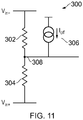
- Figure 11 illustrates a further variation of a common mode voltage feed forward circuit 300 to be included within block 120 which allows for an offset to be included.
- An offset may be useful when the input and the output need to be at different levels, for example the sensor may be at ground and the designer may wish the output voltage to be centered around VDD/2 to maximize signal swing.
- Resistors 302 and 304 are arranged in series between the input nodes Vin - and Vin + so as to form a potential divider. However in order to provide an offset of the current source (or current sink) 306 is also provided and connected to a node 308 between the resistor 302 and 304. Resistors 302 and 304 have an equal value of Rcm and the voltage offset amounts to 0.5 Rcm Ioff.
- Input common mode voltage estimating circuits may also be formed using capacitors as shown in Figure 12 .
- a first sampling capacitor 320 is in series connection with a first sampling switch 322 between a first one of the inputs, for example Vin - and a reference node 330 which may be held at a local ground.
- a second sampling capacitor 332 is provided in series with a second sampling switch 334 between the other input, for example Vin + and the reference node 330.
- the switches 322 and 332 are driven by a suitable switch control signal, such as a square wave or similar derived from a clock.
- a further capacitor 340 can be selectively connected to a node 321 intermediate the first capacitor 320 and its switch 322 by way of a further switch 342.
- the capacitor 340 can also be connected to a node 333 intermediate the second sampling capacitor 332 and the sampling switch 334 by way of switch 344.
- the switches 322 and 334 are driven on a first phase of a control clock ⁇ so as to sample the input signals Vin - and Vin + onto the sampling capacitors.
- the switches 342 and 344 can be regarded as charge transfer switches which are driven in anti-phase with the sampling switches 322 and 334. Thus, in a first phase of operation the switches 322 and 334 close so as to sample the input voltages onto the capacitors 320 and 332.
- Repeated operation of the circuit results in the voltage across the capacitor 340 representing the common mode voltage of the inputs Vin - and Vin + .
- the capacitor 340 is connected to the common mode output voltage node 24.
Landscapes
- Engineering & Computer Science (AREA)
- Power Engineering (AREA)
- Amplifiers (AREA)
Abstract
Description
- The present disclosure relates to a differential amplifier having two outputs and an improved common mode rejection performance, wherein differences between the voltages at the output nodes are substantially unaffected by changes in a common mode input voltage.
- It is known that differential amplifiers should receive first and second signals at their respective first and second inputs and to generate an output which is solely a function of the difference between the first and second signals. If the signals have a common mode component, then the value of this common mode component should not affect the output from an ideal differential amplifier.
- However, in real devices component mismatch means that the devices deviate from the ideal response characteristic and that the output shows some dependence on the common mode input voltage. There is therefore a need to improve the performance of circuits using differential amplifiers. The amount by which a common mode input signal manifests itself as a change in the output signal is often referred to as the common mode rejection ratio. It is, in essence, a measure of how well the amplifier avoids mixing the common mode signal with the differential signal.
- Often the term "amplifier" is used to refer to a circuit that provides gain. Sometimes the term is used to denote a circuit or gain block having a very high but not necessarily well controlled gain, such as an
operational amplifier 2, as shown inFigure 1a . Sometimes the term is used to encompass an arrangement where the gain block/operational amplifier 2 is provided inside a feedback loop where the overall gain of the amplifier is defined by the feedback loop, as shown inFigure 1b . - Herein when we specifically wish to distinguish between the configurations shown in
Figures 1a and 1b , then things like the arrangement ofFigure 1a will be referred to as gain block, and things like the arrangement ofFigure 1b will be referred to as "feedback defined amplifiers". -
US 7,365,600 discloses a circuit that measures the common mode value of a pair of differential input signals and uses them to cause a transconductance device to produce one or more currents to compensate the output common mode current component that flows through the feedback and input resistors of the circuit. - According to a first aspect of the present disclosure there is provided a differential amplifier comprising a target output common mode voltage input node configured to receive an input signal to set a target common mode output voltage of the differential amplifier, characterized in that the amplifier further comprises a feed forward path for adjusting the target common mode output voltage as a function of a common mode signal at differential inputs of the differential amplifier.
- The feed-forward path may be formed internally within a gain block or by components around the gain block.
- The differential amplifier can comprise a gain block having a differential input and a differential output.
- The gain of the differential amplifier can be set by a feedback network around the gain block.
- Preferably the feedback network can be a resistor based network. However in other embodiments the feedback network may include other components in addition to or in place of resistors. The other components may be operated in continuous time (unswitched) or discrete time (switched) modes.
- In an embodiment there is provided a resistor based feedback defined differential amplifier having a fully differential output, and having means for adjusting a target common mode output voltage to track changes in a common mode input signal.
- A resistor based feedback defined differential amplifier has certain advantages, such as it operates in continuous time and can be configured to have a low input impedance. These features are not available with chopped amplifiers based on switched capacitor technologies. However such resistor based technologies are more susceptible to gain errors due to component mismatching. Resistors formed on an integrated circuit may still suffer from fabrication errors resulting from slight differences in the lithography, slight variations in the amount that they are etched or the amount of material deposited or other manufacturing errors. Furthermore such resistors may then be subject to thermal gradients as a result of the operation of the circuit in which they are placed which means that the resistors might, in use, operate at different temperatures. Furthermore, the process of packaging an integrated circuit can stress the silicon die which can also give rise to changes in resistance of supposedly matched resistors. All these affects can give rise to a resistive mismatch in the gain setting network around a resistor controlled differential amplifier. A resistance mismatch of a relatively modest amount can give rise to significant reduction in the common mode rejection ratio of the amplifier.
- Advantageously the gain block, for example an operational amplifier, is associated with a circuit which modifies the target output common mode voltage as a function of the input common mode voltage. The circuit may also apply a voltage so as to shift the voltage domain (common mode voltage) between the input and output voltage ranges of the differential amplifier.
- According to a second aspect of this disclosure there is provided a method of improving the linearity of a differential amplifier in the presence of a common mode input signal component, the differential amplifier having a control node for controlling a target common mode output voltage of a differential output of the amplifier, the method comprising feeding forward a control signal to the target common mode voltage control node as a function of the input common mode voltage.
- Although the issues of component mismatch in the context of adversely affecting the common mode rejection performance, i.e. converting the common mode signal into a differential signal component, will be discussed in detail with respect to feedback defined amplifiers where the feedback loop is primarily defined by resistors, the same issues arise where the feedback loop is defined by capacitors or other components.
- Embodiments of the present disclosure will now be described, by way of non-limiting example only, with reference to the accompanying drawings, in which:
-
Figure 1a schematically represents a gain block in the form of a differential operational amplifier having a single output, andFigure 1b illustrates the use of the differential operational amplifier within a feedback defined amplifier circuit; -
Figure 2 schematically illustrates a circuit for a feedback defined differential amplifier with a single output; -
Figures 3a and 3b illustrate a circuit equivalence between two representations of voltages V1 and V2 to illustrate how a common mode voltage is defined; -
Figure 4 schematically illustrates the circuit diagram for a fully differential amplifier, namely one having differential inputs and differential outputs; -
Figure 5 schematically shows a simplified circuit diagram of a single stage differential amplifier as the type shown inFigure 1 for the purposes of introducing the modifications made to such an amplifier to make it fully differential; -
Figure 6 schematically illustrates a simplified circuit diagram of a fully differential amplifier including a common mode output voltage controller; -
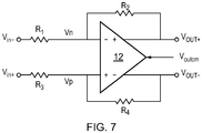
Figure 7 illustrates a circuit diagram of a feedback defined amplifier where the gain of the amplifier is set by resistors R1 to R4 of a feedback network and the output common mode voltage is controlled by a voltage fed to the common mode control terminal of the amplifier; -
Figure 8 schematically illustrates an amplifier where the common mode input voltage is used to modify the target common mode output voltage in accordance with teachings of this disclosure; -
Figure 9 shows an embodiment of a two stage amplifier where the first stage common mode voltage control based on the common mode input voltage; -
Figure 10 shows a measurement system in conjunction with an amplifier constituting an embodiment of this disclosure; -
Figure 11 is a circuit diagram of an input common mode voltage tracking circuit including an offset generator; -
Figure 12 is a circuit diagram of a switched capacitor based input common mode voltage tracking circuit; -
Figure 13 shows how the circuit ofFigure 12 may be arranged to add an offset voltage; -
Figure 14 shows a further embodiment of a feedback defined amplifier operating in accordance with the teachings of this disclosure; -
Figure 15 shows a further embodiment of a feedback defined amplifier operating in accordance with the teachings of this disclosure; and -
Figure 16 shows a further embodiment with a discrete time common mode voltage modification circuit following the fully differential amplifier. -
Figure 1a schematically illustrates the circuit diagram for a differential amplifier having a single output. As known to the person skilled in the art thedifferential amplifier 2 has an invertinginput 4 and anon-inverting input 6. The difference between those inputs is gained up by the internal gain of theamplifier 2 and the output is provided at a voltage at asingle output 8. Typically the internal gain of the amplifier is in the order of ten thousand to ten million times or more. In order to make amplifiers having their modest gains, a feedback loop generally comprising first and second resistors is provided as known to the person skilled in the art. -
Figure 1b shows the provision of a feedback loop formed by resistors R1 and R2 around the operational amplifier/gain block 2 such that the resistors define the gain of the amplifier, generally designated 10. - The circuit arrangement of
Figure 1b can be modified as shown inFigure 2 to provide a differential amplifier which accepts input voltage V1 and V2 and provides a single output voltage Vout. The ratio of the resistors
- As shown in
Figure 3a , the voltage V1 and V2 can be regarded as originating from asignal source 11 comprising first and second voltage sources V1 and V2 referenced to a common node, such as ground. However an equivalent representation is shown inFigure 3b where a voltage source provides a common mode voltage Vcm representing the average of V1 and V2, and then a further voltage Vi is added to it to create V1 and the same voltage Vi is subtracted from Vcm to make V2. - In an ideal differential feedback defined amplifier


- For convenience V1 and V2 will be referred to Vin- and Vin+.
- Considering the amplifier of
Figure 2 in greater detail, its common mode rejection ratio could be tested by shorting Vin- to Vin+ and then sweeping that input over a voltage range. Ideally the output voltage Vout would not change as the common mode input voltage swept over the input range. In general one can write an equation linking the change in output voltage to the change in input voltages in terms of a common mode gain Gcm and a differential gain Gdiff. The gain is written in small signal form (changing output voltage versus change in input voltage) as opposed to the ratio of the input and output voltages as the difference amplifier may also be used to perform a voltage translation to its input and output domains. Thus the gain could be written as

- The common mode rejection ratio, CMRR, can then be expressed as the ratio of these terms in decibels.

- The common mode rejection ratio is an important amplifier parameter. One approach of using a differential amplifier is to reject common mode signals such that a common mode voltage, or rather the target common mode voltage, at the output of the amplifier is unchanging, i.e. Gcm tends to zero.
- However, as will be shown later this approach of thinking about common mode rejection is disadvantageous in the context of some differential dual ended (e.g. two inputs and two outputs) amplifier designs.
- Differential amplifiers having dual ended (differential outputs) also can be provided.
Figure 4 schematically illustrates the symbol for such an amplifier. Here the amplifier generally designated 12 has an invertinginput 14 and anon-inverting input 16 and provides signals on first andsecond outputs mode control terminal 24. The output voltage commonmode control terminal 24 receives a common mode target voltage which is used to control the amplifier such that the average of the signals from the first andsecond outputs node 24. - For convenience, it is worth considering how the differential input stage of the
amplifier 2 shown inFigure 1a is modified in broad terms to arrive at the amplifier shown inFigure 4 . -
Figure 5 shows a simplified example of a single stage differential amplifier gain block having a single ended output, i.e. it represents one possible embodiment of the circuit shown inFigure 1 . - The circuit shown in
Figure 5 comprises first and second N-type MOSFET transistors current sink 34. The gate of thefirst transistor 30 acts as thenon-inverting input 6 and the gate of thesecond transistor 32 acts as the invertinginput 4. The transistors pass current through respective active loads which in this example are formed by two P-type MOSFETs type MOSFETs transistor 36 is connected to the drain of thetransistor 30. The drain oftransistor 38 is connected to the drain oftransistor 32. The drain oftransistor 36 is also connected to the gates of thetransistors transistor 36 is in a "diode connected" configuration and the current passing through it is mirrored bytransistor 38. An output signal is derived from the drain oftransistor 38. Thus the arrangement shown inFigure 5 has a differential input and a single ended output. This circuit can easily be modified as shown inFigure 6 to provide a differential output. The arrangement shown inFigure 6 sets out the circuit diagram of an embodiment of theamplifier 12 ofFigure 4 . The circuit comprises a differential amplifier gain block, generally designated 50 but based on the arrangement shown inFigure 5 , together with an error amplifier generally designated 52. - Comparing
Figure 6 withFigure 5 it can be seen that the first and second N-type transistors current sink 34. Furthermore thetransistors type transistors type transistors transistor 36 is no longer diode connected and instead bothtransistors error amplifier 52. A first output node O1 is still formed at the drain oftransistor 32. However a new differential output node designated O2 is now formed at the drain oftransistor 30. - In principle if all the transistors were completely matched, then the
transistors differential error amplifier 52. It comprises a differential input stage comprising N-type transistors current sink 74. Each of thetransistors type MOSFETs type MOSFET transistors type transistor 70. The target common mode output voltage Voutcm can be supplied to the gate of thefirst transistor 70 of theerror amplifier 52. The instantaneous common mode voltage of the outputs O1 and O2 of theamplifier 50 are provided to the gate of asecond transistor 72 of theerror amplifier 52. The common mode voltage is formed by placing a resistive potential divider between the outputs nodes O1 and O2. The potential divider comprisesresistors node 104 betweenresistors transistor 72. The resistors values are selected to be moderately large such that they do not adversely affect the operation of theamplifier 50. - If the common mode voltage of the outputs O1 and O2 is above Voutcm then it can be seen that more current flows to a
transistor 72 and less current flows throughtransistor 70. This causes the voltage of the drain of thetransistor 70 to rise and therefore the gate voltages of thetransistor amplifier stage 50 as a whole is set by thecurrent sink 34 and hence the voltage at nodes O1 and O2 tends to fall. Similarly if the common mode output voltage is too low thentransistor 70 tends to pass more current thantransistor 72 and as a result its drain voltage decreases. This in turn causestransistors gates transistor 70. Other amplifier topologies are known and the internal configuration of the differential gain block is not part of the inventive concept set out in this disclosure. - The differential input differential output amplifier of
Figure 5 andFigure 6 is generally connected within a circuit arrangement as shown inFigure 7 where the differential gain is set by the interaction of resistors R1 and R2 and R3 and R4. - As will be shown below, the operation of the feedback defined amplifier shown in
Figure 7 is similar to the operation of single ended operational amplifiers known to the person skilled in the art, and as illustrated inFigure 1b . However there are some nuances in the circuit design and in particular the effect of component mismatch, i.e. the ratio of resistor R2 to R1 being slightly different to the ratio of resistor R4 to R3. This, as might be expected, gives rise to a change in the differential gain of the amplifier. However, as will also be shown, it gives rise to a degradation in the common mode rejection ratio of the amplifier. - The inventor realized that an improved common mode rejection could be achieved by deliberately modifying the target common mode output voltage. This is true even though the change in common mode output voltage is larger than in certain other systems, and on the basis of the way that engineers may think about common mode rejection the circuits disclosed herein look as if they have a reduced CMRR.
- In embodiments of this disclosure, the common mode input signal value is formed and is deliberately fed forward to the target output common mode voltage control node in order to vary the target common mode voltage at the output of the amplifier. This behavior is counterintuitive as it would be expected to degrade the amplifier performance rather than improve it as it results in the common mode gain tending towards unity. However, as will be shown below, the actual performance of a dual ended differential input amplifier is quite complex and the subtleties of its operation are often overlooked or simply not appreciated by engineers.
- Circuit analysis of a fully differential amplifier is similar to that of a normal single output differential amplifier, except that it is significantly more difficult.
- Some additional complexity arises due to the additional feedback paths.
- Using the nodes identified in
Figure 7 , then - For the voltage Vn we can see that


- For ease of writing the equations, let


- Hence we can rewrite Vn and Vp as


- We can also introduce the differential gain of the amplifier as G(f)

- Combining
Equations Equation 8
- This is still cumbersome, but further progress can be made by noting that


- Now we can rewrite equation 9 as


- Using the normal assumptions of very high gain within the gain block such that
G(f)α >> 1 and G(f)β >> 1
thenEquation 12 can be reduced to

- If we define the output differential signal as


- If the resistors are matched, such that R1 = R3 and R2 = R4 then α = β. This allows simplification of
Equation 16 since if α = β then the term "2Vout(β - α)" always evaluates to zero. Assume the resistors are perfectly matched so that we can replace β by α, so


- However we can also see that if there is a small mismatch, say by a factor of 0.001 such that β = 1.001α, then two things can be observed.
- 1) Firstly the differential gain charges slightly as the first portion of
Equation 16 becomes
Thus there is a gain error that is proportional to Vin + - Vin - and independent of the common mode voltage. - 2) The second portion of
Equation 16 no longer evaluates to zero, i.e.


- Now it can be observed that the input signals Vin+ and Vin- can be related to each other by introducing a common mode input voltage Vincm and an input differential voltage Vindiff.

- If we return to
Equation 20 and rewrite using Equation 23

- It can be seen that the mismatch at the inputs introduce a gain error due to the common mode component which in turn can be considered as giving rise to an error voltage Verror at the outputs.

- This can be compared with the worked example of the modification as a result of the output common mode voltage from
Equation 22
- It can be seen that the effect resistor of mismatch can be reduced if the input common mode voltage is fed forward and used to adjust the target common mode voltage at the output.
-
Figure 8 schematically illustrates an embodiment of this disclosure in which the arrangement shown inFigure 7 is adapted by the inclusion of a common mode input voltage feedforward circuit 120. The common mode feedforward circuit 120 receives an indication of the input signals Vin- and Vin+ and uses them to form a modified output voltage common mode target value Voutcm. - In the discussion of
Figure 2 , and with the aid ofFigures 3a and 3b it was noted that in an ideal differential feedback defined amplifier.
- The present inventor has realized that in the presence of component mismatch it is better to allow an effective common mode gain to approach unity.
- This however, at first sight gives rise to a degraded common mode rejection radio using the definitions of Equation 1, even though it reduces the mixing of the differential output signal component with the common mode output signal component.
-
Figure 9 schematically illustrates an arrangement in which the offsetvoltage tracking circuit 120 merely comprises first andsecond resistors voltage control pin 24. Thus, as opposed to other circuits where this is a DC value, the arrangement shown inFigure 9 the signal supplied to the output voltage common mode control pin is deliberately varying. - However, as will be appreciated by the preceding analysis, this approach reduces the impact of the common mode voltage and the differential gain at the outputs O1 and O2 even if it results in a common mode variation of those voltages. Thus an attempt has not been made to fix the common mode voltage at the outputs to a static value but instead it is deliberately allowed to wander as a function of the common mode input voltage. This approach improves the common mode rejection performance of the amplifier.
- The amplifier stage can be followed by a
further amplifier 180 having its own common mode output voltage control terminal which in this instance may be set to a static, i.e. substantially unchanging, voltage VT. Thus thesecond amplifier stage 180 can undertake the task of transforming the differential output voltage into a domain where it has a known and fixed common mode output component. Alternatively, thesecond stage 180 may also be provided with a variable common mode output target value. The second stage may or may not be followed by a third stage which might also have a variable common mode voltage output target value or may have a fixed value. - There is a choice of how much of the common mode input voltage signal is feed forward to the amplifier's output voltage common mode control pin. Thus the variation between the input common mode voltage and a desired output common mode target may be formed and that variation may be forwarded in its entirety or merely in part. Such a choice may be made to trade off common mode rejection against amplifier headroom.
- The disclosed technique passes on the common mode signal to be handled later in the chain, but if the gain stage has a positive gain, for example say of 100, then the CMRR limitation of the next element in the chain when input referred to before this invention has effectively improved by a factor of 100, as the differential signal has been amplified, but the common mode signal gain has remained unity.
- It is thus possible to provide an improved differential amplifier with significantly improved common mode rejection ratios. In testing an amplifier having an inherent common mode rejection ratio of 60 dB was modified by the feed forward circuit to exhibit an effective common mode rejection ratio of limited by the common mode rejection ratio of the ADC measuring the output which had around -120dB CMRR.
-
Figure 10 shows an example of an amplifier in accordance with the teachings of this disclosure receiving a signal from a differentialRogowski type coil 200. The amplifier generally designated 220 amplifies the differential signal from theRogowski coil 200 and supplies it to a differential analog todigital converter 222. Theamplifier 220 is configured as an inverting amplifier and its gain set by the ratio of its input resistance to the feedback resistances. - In this scenario the input resistance comprises at least two resistors one of which RC is the resistance of the respective coil of the differential Rogowski coil sensor. The or each other resistor may be an on-chip resistor which advantageously has a lower temperature coefficient resistance than that of the Rogowski coil. The at least one other resistor has a resistance Rin. In the example shown in
Figure 10 the coil resistance is represented byresistors resistors Capacitors 
- In this example the output nodes of the amplifier are connected to
resistors resistors resistors - Furthermore, the input signals at nodes INN and INP are provided to a
common mode controller 250 which, as described hereinbefore, could simply be two resistors forming a potential divider. Thecommon mode controller 250 sets the target common mode output voltage of theamplifier 12. Thus this circuit can take a small input signal from the Rogowski coil sensor and amplify it whilst also exhibiting enhanced immunity to common mode signals. Although the common mode output voltage may not be static due to the action of thecommon mode controller 250, the differential analog to digital converter 252 can deal with that feature of the output of the amplifier and provide an output code which is independent of the common mode output voltage from theamplifier 12. - The configuration of resistors described herein also forms two potential dividers which can act to reduce the gain of the amplifier slightly as the temperature increases. Explicitly, if the temperature coefficients of the resistors on-chip are less than the temperature coefficient resistance of the coil, then the overall amplifier gain decreases or at least can be arranged to decrease slightly as the temperature increases. This effect can be used to compensate for thermal expansion of a substrate carrying the Rogowski coil or of the coil itself. The increasing volume of the coil as a function of temperature means that the output voltage of the coil for a given magnetic field acting at the coil also increases with increasing temperature. Thus these two effects can be balanced out. Thus the circuit shown in
Figure 9 can provide some temperature compensation for gain as the volume of the sensor coil increases as well as providing for improved common mode rejection. - The amplifier need not be limited to measuring currents by way of the voltage developed across a Rogowski coil. The input could come from shunt resistors, capacitive sensors, biomedical sensors or indeed any sensors having a differential output. Similarly the amplifier response does not need to be a low pass filter response, and gain adjustment as a function of temperature as described above need not be performed.
-
Figure 11 illustrates a further variation of a common mode voltage feedforward circuit 300 to be included withinblock 120 which allows for an offset to be included. An offset may be useful when the input and the output need to be at different levels, for example the sensor may be at ground and the designer may wish the output voltage to be centered around VDD/2 to maximize signal swing.Resistors node 308 between theresistor Resistors - Input common mode voltage estimating circuits may also be formed using capacitors as shown in
Figure 12 . Here afirst sampling capacitor 320 is in series connection with afirst sampling switch 322 between a first one of the inputs, for example Vin-and areference node 330 which may be held at a local ground. Similarly asecond sampling capacitor 332 is provided in series with asecond sampling switch 334 between the other input, for example Vin+ and thereference node 330. Theswitches further capacitor 340 can be selectively connected to anode 321 intermediate thefirst capacitor 320 and itsswitch 322 by way of afurther switch 342. Similarly thecapacitor 340 can also be connected to anode 333 intermediate thesecond sampling capacitor 332 and thesampling switch 334 by way ofswitch 344. Theswitches switches switches capacitors capacitors voltage storage capacitor 340. Repeated operation of the circuit results in the voltage across thecapacitor 340 representing the common mode voltage of the inputs Vin- and Vin+. Thecapacitor 340 is connected to the common modeoutput voltage node 24. - The arrangement shown in
Figure 12 can be modified to add an offset voltage from an offsetvoltage generator 350. Such an arrangement is shown inFigure 13 . Like parts are designated with like reference numerals. It can be seen, by comparingFigures 12 and13 , that the circuit ofFigure 12 is modified by the inclusion of extra sampling switches 322' and 334' between therespective sampling capacitors reference node 330. Additionally extra charge transfer switches 342' and 344' are now provided to connect the lower plate of thestorage capacitor 340 to circuit nodes 321' formed between thefirst sampling capacitor 320 and the sampling switch 322' and also to node 333' formed between thesecond sampling capacitor 332 and the additional sampling switch 334'. These additional switches allow thesampling capacitors storage capacitor 340 they are also floating such that an additional voltage provided by thevoltage generator 350 can impressed upon the output voltage provided atoutput node 360. - The amplifier, such as the arrangement of
Figure 8 , need not be a feedback defined amplifier where the feedback components only comprise resistors. Thus, as shown inFigure 14 the input resistors R1 and R3 have been replaced bycapacitors sampling switches Figure 15 . The operation of the choppingcircuits 380 allows the inputs and outputs to be swapped from side to side within the amplifier so as to reduce the effects of internal amplifier offsets. The commonmode estimation circuit 120 could equally be before the first chop switches 380, as opposed to after them. - As noted before the common mode voltage at the output of the
amplifier 12 varies more in systems in accordance with the present disclosure compared to prior art amplifier arrangements. However this variation avoids corruption of the differential gain by factors depending on the common mode voltage. It is therefore beneficial to follow the amplifier by circuits which have good common mode rejection ratios thereby allowing the voltage to be reliably translated to a fixed common mode reference voltage. This can be achieved by a relatively simple capacitor sampling circuit as shown inFigure 16 . Herecapacitors amplifier 12. The capacitors are preceded by input sampling switches 410 and 412 and followed by output gating switches 420 and 422. Theswitch 420 operates in anti-phase with theswitch 410. Similarly theswitch 422 operates in anti-phase with theswitch 412. Theswitches switches switches 432 are provided either side of thecapacitors Switch 430 is open circuit when theswitches switches amplifier 12 to be rejected. Furthermore if either of theoutput nodes amplifier 12. It is thus possible to mitigate the effect of component mismatch within the feedback defined amplifier. - The embodiments described herein are, as noted before, not intending to be limiting and features of one embodiment may be combined with features of another.
Claims (16)
- A differential amplifier comprising a target output common mode voltage input node (24) configured to receive an input signal (Voutcm) to set a target common mode output voltage of the differential amplifier, characterized in that the amplifier further comprises a feed forward path (120) for adjusting the target common mode output voltage as a function of a common mode signal at differential inputs of the differential amplifier (12).
- A differential amplifier (12) as claimed in claim 1, where the common mode signal at the inputs of the differential amplifier (12) is formed using a potential divider.
- A differential amplifier as claimed in claim 2, where the potential divider comprises resistors.
- A differential amplifier as claimed in claim 2 or 3, where a current source or voltage translator is used to modify the output of the potential divider.
- A differential amplifier as claimed in claim 2, where the potential divider comprises switched capacitors (320, 322).
- A differential amplifier as claimed in any preceding claim, where the amplifier (12) is a continuous time differential amplifier, and/or where the gain of the amplifier is set by an impedance network formed around a gain block.
- A differential amplifier as claimed in any preceding claim, where the amplifier (12) has a gain block having a first input, a second input, a first output and a second output, and where a first input node is connected to the first input by a first resistor (R1), the first input is connected to the first output by a second resistor (R2), a second input node is connected to the second input by a third resistor (R3) and the second input is connected to the second output by a fourth resistor (R4), and where the ratios of the resistor sizes control the differential and common mode gain of the amplifier.
- A differential amplifier as claimed in any preceding claim, comprising a second amplifier (180) arranged to receive an output from the differential amplifier (12), where the second amplifier (180) has a substantially static target common mode output voltage (VT).
- A differential amplifier as claimed in any preceding claim, in combination with a differential analog to digital converter.
- A differential amplifier as claimed in any preceding claim, in combination with a circuit for converting the output to a single ended output.
- A differential amplifier as claimed in any preceding claim, in combination with a differential current measurement circuit comprising a differential current sensor (200) providing first and second signal to inputs of the differential amplifier.
- A differential amplifier as claimed in claim 11, in combination with the differential current measurement circuit comprising a

- A differential amplifier as claimed in claim 11 or 12, in combination with the differential current measurement circuit including a differentially coupled Rogowski coil.
- A differential amplifier as claimed in any of claims 1 to 11, in combination with a current measurement circuit including a current sensor including a shunt, and the differential amplifier is responsive to a voltage difference developed across the shunt.
- A method of improving the common mode rejection performance of a differential amplifier having a control node for controlling a target common mode output voltage of a differential output of the amplifier, the method comprising feeding forward a control signal to set a target common mode output voltage as a function of the input common mode voltage, at differential inputs of the amplifier.
- A method as claimed in claim 15, in which one or more of the following apply:a) a fraction of the input common mode voltage is used to form the target common mode output voltage;b) substantially all of the input common mode voltage is used to form the target common mode output voltage;c) the method further comprises adding a fixed voltage to the signal used to form the target common mode output voltage so as to perform voltage domain transformation.
Applications Claiming Priority (1)
| Application Number | Priority Date | Filing Date | Title |
|---|---|---|---|
| US15/616,062 US10523166B2 (en) | 2017-06-07 | 2017-06-07 | Differential amplifier with modified common mode rejection, and to a circuit with an improved common mode rejection ratio |
Publications (1)
| Publication Number | Publication Date |
|---|---|
| EP3413462A1 true EP3413462A1 (en) | 2018-12-12 |
Family
ID=62567348
Family Applications (1)
| Application Number | Title | Priority Date | Filing Date |
|---|---|---|---|
| EP18176037.2A Pending EP3413462A1 (en) | 2017-06-07 | 2018-06-05 | Differential amplifier with modified common mode rejection, and to a circuit with an improved common mode rejection ratio |
Country Status (3)
| Country | Link |
|---|---|
| US (1) | US10523166B2 (en) |
| EP (1) | EP3413462A1 (en) |
| CN (1) | CN109004911B (en) |
Cited By (5)
| Publication number | Priority date | Publication date | Assignee | Title |
|---|---|---|---|---|
| EP3713082A1 (en) * | 2019-03-22 | 2020-09-23 | Yamaha Corporation | Amplification circuit |
| CN114268301A (en) * | 2022-02-28 | 2022-04-01 | 成都明夷电子科技有限公司 | LOS detection circuit with self-calibration offset function and detection method |
| CN115567018A (en) * | 2022-09-27 | 2023-01-03 | 无锡中微亿芯有限公司 | Chip state monitoring circuit based on self-balanced differential signal integral amplifier circuit |
| CN115668762A (en) * | 2020-03-25 | 2023-01-31 | 伯斯有限公司 | Common mode voltage controller for self-boosting push-pull amplifier |
| US20240106400A1 (en) * | 2020-12-17 | 2024-03-28 | Ams International Ag | Differential amplifier arrangement and converter arrangement |
Families Citing this family (18)
| Publication number | Priority date | Publication date | Assignee | Title |
|---|---|---|---|---|
| EP3296752B1 (en) * | 2016-09-15 | 2024-01-10 | General Electric Technology GmbH | Improvements in or relating to the measurement of current within a conductor |
| US10965254B2 (en) | 2018-06-04 | 2021-03-30 | Stmicroelectronics S.R.L. | Low noise amplifier circuit for a thermal varying resistance |
| CN109508063B (en) * | 2018-12-28 | 2024-03-15 | 西安航天民芯科技有限公司 | Error amplifier with feedforward compensation network |
| US10868536B1 (en) * | 2019-09-20 | 2020-12-15 | Analog Devices International Unlimited Company | High common-mode transient immunity high voltage level shifter |
| US11990879B2 (en) * | 2020-05-11 | 2024-05-21 | Texas Instruments Incorporated | Fully-differential amplifier with input common-mode voltage control |
| US11973469B2 (en) | 2020-08-12 | 2024-04-30 | Qorvo Us, Inc. | Systems and methods for providing an envelope tracking supply voltage |
| US11929712B2 (en) | 2020-08-12 | 2024-03-12 | Qorvo Us, Inc. | Delay-compensating power management circuit |
| US11923812B2 (en) | 2020-08-12 | 2024-03-05 | Qorvo Us, Inc. | Delay-compensating power management integrated circuit |
| CN114236221B (en) * | 2021-10-13 | 2023-09-26 | 北京华峰测控技术股份有限公司 | Differential voltage measurement circuit, device and method |
| CN114900183B (en) * | 2022-05-18 | 2026-03-24 | 重庆吉芯科技有限公司 | Input common-mode compensation circuit, pipelined analog-to-digital converter and input common-mode compensation method |
| US20230412132A1 (en) * | 2022-06-16 | 2023-12-21 | Apple Inc. | Voltage Generation Circuitry with Reduced Settling Time |
| CN115347870A (en) * | 2022-07-29 | 2022-11-15 | 上海韦孜美电子科技有限公司 | Novel differential amplifier and equipment with feedforward bias correction circuit |
| CN115511473B (en) * | 2022-11-02 | 2023-04-18 | 北京共识数信科技有限公司 | Smart letter management method, system and storage medium based on big data |
| DE102023200490A1 (en) | 2023-01-24 | 2024-07-25 | Robert Bosch Gesellschaft mit beschränkter Haftung | Differential amplifier for operating a sensor |
| CN116299126B (en) * | 2023-05-16 | 2023-08-29 | 上海安其威微电子科技有限公司 | Calibration circuit, system, method, control unit, storage medium, and program product |
| CN117176164A (en) * | 2023-09-04 | 2023-12-05 | 国仪量子(合肥)技术有限公司 | Data acquisition circuit, data acquisition card |
| CN117176166A (en) * | 2023-09-04 | 2023-12-05 | 国仪量子(合肥)技术有限公司 | Data acquisition circuit, data acquisition card |
| CN118449476B (en) * | 2024-07-08 | 2024-10-15 | 江苏鑫康微电子科技有限公司 | Trimming device for improving PGA common mode rejection ratio |
Citations (4)
| Publication number | Priority date | Publication date | Assignee | Title |
|---|---|---|---|---|
| US5864257A (en) * | 1997-07-15 | 1999-01-26 | Exar Corporation | Replica bias circuit to optimize swing of differential op-amp |
| US20060091931A1 (en) * | 2004-10-29 | 2006-05-04 | John Leete | System and method for common mode bias for high frequency buffers |
| US7365600B1 (en) | 2005-06-02 | 2008-04-29 | Linear Technology Corporation | Non-feedback implemented control of the output-common mode of a differential amplifier |
| US20110026180A1 (en) * | 2009-07-30 | 2011-02-03 | Haible Juergen | Integrator and circuit-breaker having an integrator |
Family Cites Families (13)
| Publication number | Priority date | Publication date | Assignee | Title |
|---|---|---|---|---|
| US6317068B1 (en) * | 1999-08-23 | 2001-11-13 | Level One Communications, Inc. | Method and apparatus for matching common mode output voltage at a switched-capacitor to continuous-time interface |
| EP1168603A1 (en) * | 2000-06-26 | 2002-01-02 | STMicroelectronics S.r.l. | Switched-capacitor, fully-differential operational amplifier with high switching frequency |
| US6891435B2 (en) * | 2002-12-13 | 2005-05-10 | Microtune (Texas), L.P. | System and method for reducing second order distortion in electronic circuits |
| US7221190B2 (en) * | 2005-03-14 | 2007-05-22 | Texas Instruments Incorporated | Differential comparator with extended common mode voltage range |
| US7375585B2 (en) * | 2005-05-02 | 2008-05-20 | Texas Instruments Incorporated | Circuit and method for switching active loads of operational amplifier input stage |
| US7893766B1 (en) * | 2009-09-10 | 2011-02-22 | International Business Machines Corporation | Adaptive common mode bias for differential amplifier input circuits |
| US8279004B2 (en) * | 2010-07-01 | 2012-10-02 | Global Unichip Corp. | System for driver amplifier |
| US9264002B2 (en) * | 2014-02-19 | 2016-02-16 | Analog Devices Global | Apparatus and methods for improving common mode rejection ratio |
| US9209789B1 (en) * | 2014-08-13 | 2015-12-08 | Qualcomm Incorporated | Apparatus to convert electrical signals from small-signal format to rail-to-rail format |
| US9438188B2 (en) * | 2014-09-15 | 2016-09-06 | Qualcomm Incorporated | Common-gate amplifier for high-speed DC-coupling communications |
| CN205693639U (en) * | 2016-03-10 | 2016-11-16 | 北京联盛德微电子有限责任公司 | A kind of Full differential operational amplifier based on feedforward with weak positive feedback |
| CN105811889B (en) * | 2016-04-20 | 2019-03-05 | 佛山臻智微芯科技有限公司 | A Feedforward Compensated Transconductance Operational Amplifier |
| US10320337B2 (en) * | 2016-08-30 | 2019-06-11 | Cirrus Logic, Inc. | Fully-differential operational amplifier system |
-
2017
- 2017-06-07 US US15/616,062 patent/US10523166B2/en active Active
-
2018
- 2018-06-05 EP EP18176037.2A patent/EP3413462A1/en active Pending
- 2018-06-07 CN CN201810614404.8A patent/CN109004911B/en active Active
Patent Citations (4)
| Publication number | Priority date | Publication date | Assignee | Title |
|---|---|---|---|---|
| US5864257A (en) * | 1997-07-15 | 1999-01-26 | Exar Corporation | Replica bias circuit to optimize swing of differential op-amp |
| US20060091931A1 (en) * | 2004-10-29 | 2006-05-04 | John Leete | System and method for common mode bias for high frequency buffers |
| US7365600B1 (en) | 2005-06-02 | 2008-04-29 | Linear Technology Corporation | Non-feedback implemented control of the output-common mode of a differential amplifier |
| US20110026180A1 (en) * | 2009-07-30 | 2011-02-03 | Haible Juergen | Integrator and circuit-breaker having an integrator |
Cited By (6)
| Publication number | Priority date | Publication date | Assignee | Title |
|---|---|---|---|---|
| EP3713082A1 (en) * | 2019-03-22 | 2020-09-23 | Yamaha Corporation | Amplification circuit |
| CN115668762A (en) * | 2020-03-25 | 2023-01-31 | 伯斯有限公司 | Common mode voltage controller for self-boosting push-pull amplifier |
| US20240106400A1 (en) * | 2020-12-17 | 2024-03-28 | Ams International Ag | Differential amplifier arrangement and converter arrangement |
| CN114268301A (en) * | 2022-02-28 | 2022-04-01 | 成都明夷电子科技有限公司 | LOS detection circuit with self-calibration offset function and detection method |
| CN114268301B (en) * | 2022-02-28 | 2022-06-14 | 成都明夷电子科技有限公司 | LOS detection circuit with self-calibration offset function and detection method |
| CN115567018A (en) * | 2022-09-27 | 2023-01-03 | 无锡中微亿芯有限公司 | Chip state monitoring circuit based on self-balanced differential signal integral amplifier circuit |
Also Published As
| Publication number | Publication date |
|---|---|
| CN109004911B (en) | 2023-12-01 |
| US20180358942A1 (en) | 2018-12-13 |
| US10523166B2 (en) | 2019-12-31 |
| CN109004911A (en) | 2018-12-14 |
Similar Documents
| Publication | Publication Date | Title |
|---|---|---|
| US10523166B2 (en) | Differential amplifier with modified common mode rejection, and to a circuit with an improved common mode rejection ratio | |
| EP2839579B1 (en) | High side current sense amplifier | |
| US7944287B2 (en) | Low-noise, wide offset range, programmable input offset amplifier front end and method | |
| Carrillo et al. | Constant-g/sub m/constant-slew-rate high-bandwidth low-voltage rail-to-rail CMOS input stage for VLSI cell libraries | |
| US8072262B1 (en) | Low input bias current chopping switch circuit and method | |
| US11082012B2 (en) | Highly linear input and output rail-to-rail amplifier | |
| EP1914887B1 (en) | Differential amplifier with current source controlled through differential feedback | |
| US10116268B2 (en) | Operational amplifier | |
| US9231542B1 (en) | Amplifier common-mode control method | |
| US6717451B1 (en) | Precision analog level shifter with programmable options | |
| US7295068B2 (en) | Increasing the linearity of a transconductance cell | |
| US7859339B2 (en) | Differential amplification circuit | |
| US9893704B2 (en) | Circuit with an RC-filter | |
| US9246455B2 (en) | Three stage amplifier | |
| US9768758B2 (en) | Comparison circuit | |
| KR102818493B1 (en) | Low noise charge amplifying device and comparator | |
| Fan et al. | Input characteristics of a chopped multi-path current feedback instrumentation amplifier | |
| JP4417673B2 (en) | Electric meter signal input circuit | |
| US11824504B2 (en) | Error amplifier device | |
| US9134360B2 (en) | Method and apparatus for feedback-based resistance calibration | |
| US7812668B2 (en) | Multi-input operational amplifier and method for reducing input offset thereof | |
| WO2023233793A1 (en) | Sensor amplification circuit | |
| Stan et al. | High precision bidirectional chopper instrumentation amplifier with negative and positive input common mode range | |
| JP2016086230A (en) | Sensor device | |
| Sbaa et al. | A CMOS transconductor with high linear range |
Legal Events
| Date | Code | Title | Description |
|---|---|---|---|
| PUAI | Public reference made under article 153(3) epc to a published international application that has entered the european phase |
Free format text: ORIGINAL CODE: 0009012 |
|
| STAA | Information on the status of an ep patent application or granted ep patent |
Free format text: STATUS: THE APPLICATION HAS BEEN PUBLISHED |
|
| AK | Designated contracting states |
Kind code of ref document: A1 Designated state(s): AL AT BE BG CH CY CZ DE DK EE ES FI FR GB GR HR HU IE IS IT LI LT LU LV MC MK MT NL NO PL PT RO RS SE SI SK SM TR |
|
| AX | Request for extension of the european patent |
Extension state: BA ME |
|
| STAA | Information on the status of an ep patent application or granted ep patent |
Free format text: STATUS: REQUEST FOR EXAMINATION WAS MADE |
|
| 17P | Request for examination filed |
Effective date: 20190610 |
|
| RBV | Designated contracting states (corrected) |
Designated state(s): AL AT BE BG CH CY CZ DE DK EE ES FI FR GB GR HR HU IE IS IT LI LT LU LV MC MK MT NL NO PL PT RO RS SE SI SK SM TR |
|
| STAA | Information on the status of an ep patent application or granted ep patent |
Free format text: STATUS: EXAMINATION IS IN PROGRESS |
|
| 17Q | First examination report despatched |
Effective date: 20201209 |
|
| RAP1 | Party data changed (applicant data changed or rights of an application transferred) |
Owner name: ANALOG DEVICES INTERNATIONAL UNLIMITED COMPANY |
|
| GRAP | Despatch of communication of intention to grant a patent |
Free format text: ORIGINAL CODE: EPIDOSNIGR1 |
|
| STAA | Information on the status of an ep patent application or granted ep patent |
Free format text: STATUS: GRANT OF PATENT IS INTENDED |
|
| INTG | Intention to grant announced |
Effective date: 20251210 |
|
| GRAJ | Information related to disapproval of communication of intention to grant by the applicant or resumption of examination proceedings by the epo deleted |
Free format text: ORIGINAL CODE: EPIDOSDIGR1 |
|
| STAA | Information on the status of an ep patent application or granted ep patent |
Free format text: STATUS: EXAMINATION IS IN PROGRESS |
|
| GRAP | Despatch of communication of intention to grant a patent |
Free format text: ORIGINAL CODE: EPIDOSNIGR1 |
|
| STAA | Information on the status of an ep patent application or granted ep patent |
Free format text: STATUS: GRANT OF PATENT IS INTENDED |
|
| INTC | Intention to grant announced (deleted) | ||
| INTG | Intention to grant announced |
Effective date: 20260305 |