EP3413402A1 - Configurable docking connector - Google Patents
Configurable docking connector Download PDFInfo
- Publication number
- EP3413402A1 EP3413402A1 EP18176681.7A EP18176681A EP3413402A1 EP 3413402 A1 EP3413402 A1 EP 3413402A1 EP 18176681 A EP18176681 A EP 18176681A EP 3413402 A1 EP3413402 A1 EP 3413402A1
- Authority
- EP
- European Patent Office
- Prior art keywords
- frame members
- docking connector
- frame
- receiver
- modules
- Prior art date
- Legal status (The legal status is an assumption and is not a legal conclusion. Google has not performed a legal analysis and makes no representation as to the accuracy of the status listed.)
- Granted
Links
Images


Classifications
-
- H—ELECTRICITY
- H01—ELECTRIC ELEMENTS
- H01R—ELECTRICALLY-CONDUCTIVE CONNECTIONS; STRUCTURAL ASSOCIATIONS OF A PLURALITY OF MUTUALLY-INSULATED ELECTRICAL CONNECTING ELEMENTS; COUPLING DEVICES; CURRENT COLLECTORS
- H01R13/00—Details of coupling devices of the kinds covered by groups H01R12/70 or H01R24/00 - H01R33/00
- H01R13/46—Bases; Cases
- H01R13/516—Means for holding or embracing insulating body, e.g. casing, hoods
- H01R13/518—Means for holding or embracing insulating body, e.g. casing, hoods for holding or embracing several coupling parts, e.g. frames
-
- H—ELECTRICITY
- H01—ELECTRIC ELEMENTS
- H01R—ELECTRICALLY-CONDUCTIVE CONNECTIONS; STRUCTURAL ASSOCIATIONS OF A PLURALITY OF MUTUALLY-INSULATED ELECTRICAL CONNECTING ELEMENTS; COUPLING DEVICES; CURRENT COLLECTORS
- H01R13/00—Details of coupling devices of the kinds covered by groups H01R12/70 or H01R24/00 - H01R33/00
- H01R13/46—Bases; Cases
- H01R13/514—Bases; Cases composed as a modular blocks or assembly, i.e. composed of co-operating parts provided with contact members or holding contact members between them
-
- H—ELECTRICITY
- H01—ELECTRIC ELEMENTS
- H01R—ELECTRICALLY-CONDUCTIVE CONNECTIONS; STRUCTURAL ASSOCIATIONS OF A PLURALITY OF MUTUALLY-INSULATED ELECTRICAL CONNECTING ELEMENTS; COUPLING DEVICES; CURRENT COLLECTORS
- H01R13/00—Details of coupling devices of the kinds covered by groups H01R12/70 or H01R24/00 - H01R33/00
- H01R13/58—Means for relieving strain on wire connection, e.g. cord grip, for avoiding loosening of connections between wires and terminals within a coupling device terminating a cable
- H01R13/5837—Means for relieving strain on wire connection, e.g. cord grip, for avoiding loosening of connections between wires and terminals within a coupling device terminating a cable specially adapted for accommodating various sized cables
-
- H—ELECTRICITY
- H01—ELECTRIC ELEMENTS
- H01R—ELECTRICALLY-CONDUCTIVE CONNECTIONS; STRUCTURAL ASSOCIATIONS OF A PLURALITY OF MUTUALLY-INSULATED ELECTRICAL CONNECTING ELEMENTS; COUPLING DEVICES; CURRENT COLLECTORS
- H01R31/00—Coupling parts supported only by co-operation with counterpart
- H01R31/06—Intermediate parts for linking two coupling parts, e.g. adapter
-
- G—PHYSICS
- G01—MEASURING; TESTING
- G01R—MEASURING ELECTRIC VARIABLES; MEASURING MAGNETIC VARIABLES
- G01R1/00—Details of instruments or arrangements of the types included in groups G01R5/00 - G01R13/00 and G01R31/00
- G01R1/02—General constructional details
- G01R1/04—Housings; Supporting members; Arrangements of terminals
- G01R1/0408—Test fixtures or contact fields; Connectors or connecting adaptors; Test clips; Test sockets
- G01R1/0416—Connectors, terminals
-
- H—ELECTRICITY
- H01—ELECTRIC ELEMENTS
- H01R—ELECTRICALLY-CONDUCTIVE CONNECTIONS; STRUCTURAL ASSOCIATIONS OF A PLURALITY OF MUTUALLY-INSULATED ELECTRICAL CONNECTING ELEMENTS; COUPLING DEVICES; CURRENT COLLECTORS
- H01R2201/00—Connectors or connections adapted for particular applications
- H01R2201/20—Connectors or connections adapted for particular applications for testing or measuring purposes
Definitions
- the present invention relates to a docking connector for holding modules for connector pins.
- the interface devices come in a wide variety of sizes that can hold small number of contacts or very large numbers of contacts.
- the receiver and test adapter in an interface device typically each have a frame that holds a plurality of modules.
- the different types of interface devices often have modules of different dimensions such that modules from one interface type cannot be used in a different interface type.
- U.S. Patent No. 8,351,218 discloses an interface device having multiple tiers such that modules of a first size can be mounted in the receiver or test adapter in one tier and modules of a second size can be mounted in the receiver or test adapter in a second tier. In this manner, modules of different sizes can be used simultaneously in the same interface device.
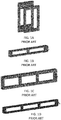
- FIGs. 1A-1D and 2 Exemplary prior docking connectors are shown in FIGs. 1A-1D and 2 . Each of these prior docking connectors has two pairs of opposing sides to form a rectangular or square frame. As shown in the example in FIG. 1A , one pair of opposing sides, the top and bottom in FIG. 1A , has holes or other means for connecting a plurality of modules to the frame in a side-by-side manner. In other examples such as are shown in FIGs. 1B-1D , the frame includes intermediate members having holes or other means for connecting modules between the intermediate members and a side or between two intermediate members.
- the present invention is a docking connector having two pairs of opposing sides forming a frame and first means on a first pair of opposing sides for mounting a plurality of connector modules in a first direction in the frame and second means on a second pair of sides for mounting a plurality of modules of a second size in a second direction where the second direction is perpendicular to the first direction.
- the present invention is a configurable docking connector.
- the configurable docking connector comprises first and second pairs of opposing sides forming a rectangular frame having an opening formed by the first and second pairs of opposing sides for receiving a plurality of connector modules.
- the first pair of opposing sides each has a plurality of mounting means configured to mount a plurality of first connector modules of a first size to the first pair of opposing sides in the opening.
- the second pair of opposing sides each having a plurality of mounting means configured to mount a plurality of second modules of a second size different from the first size to the second pair of opposing sides in a second direction where the second direction is perpendicular to the first direction.
- the configurable docking connector may be a receiver frame or a test adapter frame of an electrical interface.
- the configurable docking connector may further comprise a plurality of contact modules mounted to each of the first pair of opposing sides.
- the configurable docking connector may further comprise a plurality of contact modules mounted to each of the second pair of opposing sides.
- the first pair of opposing sides each may have means for mounting a strain relief plate, such as a mounting surface or a mounting slot or hole.
- the present invention is a configurable docking connector having a receiver comprised of first, second, third and fourth frame members arranged to form a rectangular frame having a central opening, the first and third frame members being parallel to one another and forming a length of the rectangular frame, and the second and fourth frame members being parallel to one another and forming a width of the rectangular frame, the width being less than the length.
- the first and third frame members each have a plurality of mounting means configured to mount contact modules to the first and third frame members across the central opening.
- the second and fourth frame members each have a plurality of mounting means configured to mount contact modules to the second and fourth frame members across the central opening.
- the receiver further may comprise an alignment hole in each of the first and third frame members of the receiver. The alignment holes may be polarized by being off-center in each of the first and third frame members.
- the configurable docking connector may further comprise a test adapter configured to mate with the receiver.
- the test adapter may comprise first, second, third and fourth frame members arranged to form a rectangular frame having a central opening, the first and third frame members being parallel to one another and forming a length of the rectangular frame, and the second and fourth frame members being parallel to one another and forming a width of the rectangular frame, the width being less than the length.
- the first and third frame members each may have a plurality of mounting means configured to mount contact modules to the first and third frame members across the central opening.
- the second and fourth frame members each have a plurality of mounting means configured to mount contact modules to the second and fourth frame members across the central opening.
- the receiver further may comprise an alignment hole in each of the first and third frame members of the receiver and the test adapter further comprises an alignment pin extending from each of the first and third frame members of the test adapter.
- the alignment holes are polarized by being off-center in each of the first and third frame members of the receiver and the alignment pins are correspondingly polarized by being off-center in each of the first and third frame members of the test adapter.
- the test adapter further comprises an alignment hole in each of the first and third frame members of the test adapter and the receiver further comprises an alignment pin extending from each of the first and third frame members of the receiver.
- the alignment holes may be polarized by being off-center in each of the first and third frame members of the test adapter and the alignment pins are correspondingly polarized by being off-center in each of the first and third frame members of the receiver.
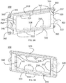
- FIGs. 3A-3G A first side 300 of a docking connector in accordance with a preferred embodiment of the present invention is shown in FIGs. 3A-3G .
- this first side will be referred to as the test adapter, but the two sides of the docking connector of the present invention could be reversed such that this first side would be connected to test equipment and therefore be a receiver.
- the test adapter 300 has a frame formed from two pairs of opposing members 310, 320 and 330, 340. In FIGs.
- members 310, 320 could be referred to as the "top” and “bottom” while members 330, 340 could be referred to as sides, but the docking connector can be oriented perpendicular to that shown in FIGs. 3A-3G and thus the top/bottom and sides nomenclature would be reversed.
- Opposing members 310, 320 respectively have holes 312, 322 for mounting a plurality of connector modules of a first size between the members 310, 320.
- Opposing members 330, 340 respectively have holes 332, 342 for mounting a plurality of connector modules of a second size between the members 330, 340.
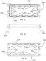
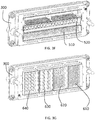
- FIGs. 3F and 3G when modules 610, 620, 630, 640 of the first size are mounted in the frame between members 310, 320 they would have their length in a first direction (vertical in FIG. 3G ) and when modules 510, 520 of the second size are mounted in the frame between members 330, 340 they would have their length in a second direction (horizontal in FIG.
- a single docking connector may be used alternatively to house to different sizes of modules.
- Each of the first plurality of modules or the second plurality of modules may be different types, meaning that they could hold different kinds of connectors or different mixtures of connectors.
- the first side 300 of the docking connector has surfaces 316 and 326 on members 310 and 320 for mounting strain relief plates to support various types of wires.
- Members 310, 320 further have slots 318 and 328 for mounting strain relief plates. It further may have coring 314, 324 to reduce the mass of the docking connector.
- the docking connector for example, may be die cast or machined metal.
- the docking connector has mounting screws 360 to mount the first side 300 to test equipment or to a unit under test. There is a floating bushing (not shown) and a washer 362 beneath the head of each screw 360.
- the washer 362 may be a low friction material such as nylon.
- the first side 300 of the docking connector further has alignment pins 350 for aligning the first side 300 with the second side 400, which has corresponding holes 450 for receiving the pins 300.
- the pins 350 are off-center, i.e., close to member 320 than to member 310, to provide polarization to ensure that the two sides 300, 400 of the docking connector are properly placed together.
- the first side 300 further has tapped holes 334 (in FIG. 3A ) and 336 (in FIG. 3B ) for an earth ground screw.
- FIGs. 3A-3G show a first side 300 of a docking connector
- FIGs. 4A-4G show a second side 400 of a docking connector that mates with the first side 300. Since the first side 300 was referred to as a test adapter above, the second side 400 will be referred to herein as a receiver 400. One of skill in the art, however, will understand that the first and second sides could be arranged in an opposite manner.
- the receiver 400 has a frame formed from two pairs of opposing members 410, 420 and 430, 440.
- members 410, 420 could be referred to as the "top” and “bottom” while members 430, 440 could be referred to as sides, but the docking connector can be oriented perpendicular to that shown in FIGs. 4A-4G and thus the top/bottom and sides nomenclature would be reversed.
- Opposing members 410, 420 respectively have holes 412, 422 for mounting a plurality of connector modules of a first size to and between the members 410, 420.
- Opposing members 430, 440 respectively have holes 432, 442 for mounting a plurality of connector modules of a second size to and between the members 430, 440.
- FIGs. 4F and 4G when modules 810, 820, 830, 840 of the first size are mounted in the frame between members 410, 420 they would have their length in a first direction (vertical in FIG. 4G ) and when modules 710, 720 of the second size are mounted in the frame between members 430, 440 they would have their length in a second direction (horizontal in FIG.
- a single docking connector may be used alternatively to house to different sizes of modules.
- Each of the first plurality of modules or the second plurality of modules may be different types, meaning that they could hold different kinds of connectors or different mixtures of connectors.
- the second side 400 of the docking connector has surfaces 416 and 426 on members 410 and 420 for mounting strain relief plates to support various types of wires.
- Members 410, 420 further have slots 418 and 428 for mounting strain relief plates.
- It further may have coring 414, 424 to reduce the mass of the docking connector.
- the docking connector has mounting screws 460 to mount the second side 400 to test equipment or to a unit under test.
- the washer 462 may be a low friction material such as nylon.
- the second side 400 of the docking connector further has alignment 450 for aligning the second side 400 with the first side 300, which has corresponding alignment pins 350 that are received the alignment holes 450 when the first and second sides are mated.
- the alignment holes 450 are off-center, i.e., closer to member 420 than to member 410, to provide polarization to ensure that the two sides 300, 400 of the docking connector are properly placed together.
- the second side 400 further has tapped holes 434 (in FIG. 4A ) and 436 (in FIG. 4B ) for an earth ground screw.
Landscapes
- Details Of Connecting Devices For Male And Female Coupling (AREA)
Abstract
Description
- The present application claims the benefit of the filing date of
U.S. Provisional Patent Application Serial No. 62/516,971 filed on June 8, 2017 - The aforementioned provisional patent application is hereby incorporated by reference in its entirety.
- The present invention relates to a docking connector for holding modules for connector pins.
- A variety of electrical interface devices exist for housing modules that hold electrical and/or pneumatic contacts of various types. Examples of such interface devices are disclosed in
U.S. Patent No. 7,091,415 ,U.S. Patent No. 7,297,014 ,U.S. Patent No. 8,348,693 andU.S. Patent No. 9,257,787 - The receiver and test adapter in an interface device typically each have a frame that holds a plurality of modules. The different types of interface devices often have modules of different dimensions such that modules from one interface type cannot be used in a different interface type. To overcome this problem,
U.S. Patent No. 8,351,218 discloses an interface device having multiple tiers such that modules of a first size can be mounted in the receiver or test adapter in one tier and modules of a second size can be mounted in the receiver or test adapter in a second tier. In this manner, modules of different sizes can be used simultaneously in the same interface device. - In small applications an engagement mechanism may not be necessary so a frame, referred to herein as a "docking connector," is used to hold connector modules filled with connector pins improve connection times. Exemplary prior docking connectors are shown in
FIGs. 1A-1D and2 . Each of these prior docking connectors has two pairs of opposing sides to form a rectangular or square frame. As shown in the example inFIG. 1A , one pair of opposing sides, the top and bottom inFIG. 1A , has holes or other means for connecting a plurality of modules to the frame in a side-by-side manner. In other examples such as are shown inFIGs. 1B-1D , the frame includes intermediate members having holes or other means for connecting modules between the intermediate members and a side or between two intermediate members. - In a preferred embodiment, the present invention is a docking connector having two pairs of opposing sides forming a frame and first means on a first pair of opposing sides for mounting a plurality of connector modules in a first direction in the frame and second means on a second pair of sides for mounting a plurality of modules of a second size in a second direction where the second direction is perpendicular to the first direction.
- In another preferred embodiment, the present invention is a configurable docking connector. The configurable docking connector comprises first and second pairs of opposing sides forming a rectangular frame having an opening formed by the first and second pairs of opposing sides for receiving a plurality of connector modules. The first pair of opposing sides each has a plurality of mounting means configured to mount a plurality of first connector modules of a first size to the first pair of opposing sides in the opening. The second pair of opposing sides each having a plurality of mounting means configured to mount a plurality of second modules of a second size different from the first size to the second pair of opposing sides in a second direction where the second direction is perpendicular to the first direction. The configurable docking connector may be a receiver frame or a test adapter frame of an electrical interface. The configurable docking connector may further comprise a plurality of contact modules mounted to each of the first pair of opposing sides. Alternatively, the configurable docking connector may further comprise a plurality of contact modules mounted to each of the second pair of opposing sides. The first pair of opposing sides each may have means for mounting a strain relief plate, such as a mounting surface or a mounting slot or hole.
- In another preferred embodiment, the present invention is a configurable docking connector having a receiver comprised of first, second, third and fourth frame members arranged to form a rectangular frame having a central opening, the first and third frame members being parallel to one another and forming a length of the rectangular frame, and the second and fourth frame members being parallel to one another and forming a width of the rectangular frame, the width being less than the length. The first and third frame members each have a plurality of mounting means configured to mount contact modules to the first and third frame members across the central opening. The second and fourth frame members each have a plurality of mounting means configured to mount contact modules to the second and fourth frame members across the central opening. The receiver further may comprise an alignment hole in each of the first and third frame members of the receiver. The alignment holes may be polarized by being off-center in each of the first and third frame members.
- The configurable docking connector may further comprise a test adapter configured to mate with the receiver. The test adapter may comprise first, second, third and fourth frame members arranged to form a rectangular frame having a central opening, the first and third frame members being parallel to one another and forming a length of the rectangular frame, and the second and fourth frame members being parallel to one another and forming a width of the rectangular frame, the width being less than the length. The first and third frame members each may have a plurality of mounting means configured to mount contact modules to the first and third frame members across the central opening. The second and fourth frame members each have a plurality of mounting means configured to mount contact modules to the second and fourth frame members across the central opening. The receiver further may comprise an alignment hole in each of the first and third frame members of the receiver and the test adapter further comprises an alignment pin extending from each of the first and third frame members of the test adapter. The alignment holes are polarized by being off-center in each of the first and third frame members of the receiver and the alignment pins are correspondingly polarized by being off-center in each of the first and third frame members of the test adapter. Alternatively, the test adapter further comprises an alignment hole in each of the first and third frame members of the test adapter and the receiver further comprises an alignment pin extending from each of the first and third frame members of the receiver. Again, the alignment holes may be polarized by being off-center in each of the first and third frame members of the test adapter and the alignment pins are correspondingly polarized by being off-center in each of the first and third frame members of the receiver.
- Still other aspects, features, and advantages of the present invention are readily apparent from the following detailed description, simply by illustrating a preferable embodiments and implementations. The present invention is also capable of other and different embodiments and its several details can be modified in various obvious respects, all without departing from the spirit and scope of the present invention. Accordingly, the drawings and descriptions are to be regarded as illustrative in nature, and not as restrictive. Additional objects and advantages of the invention will be set forth in part in the description which follows and in part will be obvious from the description or may be learned by practice of the invention.
- For a more complete understanding of the present invention and the advantages thereof, reference is now made to the following description and the accompanying drawings, in which:
-
FIGs. 1A-1D are perspective view of prior art docking connectors. -
FIG. 2 is a perspective view of a prior art docking connector. -
FIG. 3A is a front perspective view of a first side of a docking connector in accordance with a preferred embodiment of the present invention. -
FIG. 3B is a rear perspective view of a first side of a docking connector in accordance with a preferred embodiment of the present invention. -
FIG. 3C is a front view of a first side of a docking connector in accordance with a preferred embodiment of the present invention. -
FIG. 3D is a side view of a first side of a docking connector in accordance with a preferred embodiment of the present invention. -
FIG. 3E is a rear view of a first side of a docking connector in accordance with a preferred embodiment of the present invention. -
FIG. 3F is a front perspective view of a first side of a docking connector in accordance with a preferred embodiment of the present invention with a plurality of modules of a first size mounted in the docking connector in a first direction. -
FIG. 3G is a front perspective view of a first side of a docking connector in accordance with a preferred embodiment of the present invention with a plurality of modules of a second size mounted in the docking connector in a second direction perpendicular to the first direction. -
FIG. 4A is a front perspective view of a second side of a docking connector in accordance with a preferred embodiment of the present invention. -
FIG. 4B is a rear perspective view of a second side of a docking connector in accordance with a preferred embodiment of the present invention. -
FIG. 4C is a front view of a second side of a docking connector in accordance with a preferred embodiment of the present invention. -
FIG. 4D is a side view of a second side of a docking connector in accordance with a preferred embodiment of the present invention. -
FIG. 4E is a rear view of a second side of a docking connector in accordance with a preferred embodiment of the present invention. -
FIG. 4F is a front perspective view of a second side of a docking connector in accordance with a preferred embodiment of the present invention with a plurality of modules of a first size mounted in the docking connector in a first direction. -
FIG. 4G is a front perspective view of a second side of a docking connector in accordance with a preferred embodiment of the present invention with a plurality of modules of a second size mounted in the docking connector in a second direction perpendicular to the first direction. - The preferred embodiments of the inventions are described with reference to the drawings. A
first side 300 of a docking connector in accordance with a preferred embodiment of the present invention is shown inFIGs. 3A-3G . In this description, this first side will be referred to as the test adapter, but the two sides of the docking connector of the present invention could be reversed such that this first side would be connected to test equipment and therefore be a receiver. Thetest adapter 300 has a frame formed from two pairs of opposingmembers FIGs. 3A-3G ,members members FIGs. 3A-3G and thus the top/bottom and sides nomenclature would be reversed. - Opposing
members holes members members holes members FIGs. 3F and 3G , whenmodules members FIG. 3G ) and whenmodules members FIG. 3F ) that is perpendicular to the first direction. In this manner, a single docking connector may be used alternatively to house to different sizes of modules. Each of the first plurality of modules or the second plurality of modules may be different types, meaning that they could hold different kinds of connectors or different mixtures of connectors. - As shown in
FIG. 3A , thefirst side 300 of the docking connector hassurfaces members Members slots coring screws 360 to mount thefirst side 300 to test equipment or to a unit under test. There is a floating bushing (not shown) and awasher 362 beneath the head of eachscrew 360. Thewasher 362 may be a low friction material such as nylon. Thefirst side 300 of the docking connector further hasalignment pins 350 for aligning thefirst side 300 with thesecond side 400, which has correspondingholes 450 for receiving thepins 300. Thepins 350 are off-center, i.e., close tomember 320 than tomember 310, to provide polarization to ensure that the twosides first side 300 further has tapped holes 334 (inFIG. 3A ) and 336 (inFIG. 3B ) for an earth ground screw. - While
FIGs. 3A-3G show afirst side 300 of a docking connector,FIGs. 4A-4G show asecond side 400 of a docking connector that mates with thefirst side 300. Since thefirst side 300 was referred to as a test adapter above, thesecond side 400 will be referred to herein as areceiver 400. One of skill in the art, however, will understand that the first and second sides could be arranged in an opposite manner. - The
receiver 400 has a frame formed from two pairs of opposingmembers FIGs. 4A-4G ,members members FIGs. 4A-4G and thus the top/bottom and sides nomenclature would be reversed. - Opposing
members holes members members holes members FIGs. 4F and 4G , whenmodules members FIG. 4G ) and whenmodules members FIG. 4F ) that is perpendicular to the first direction. In this manner, a single docking connector may be used alternatively to house to different sizes of modules. Each of the first plurality of modules or the second plurality of modules may be different types, meaning that they could hold different kinds of connectors or different mixtures of connectors. - As shown in
FIG. 4A , thesecond side 400 of the docking connector hassurfaces members Members slots coring second side 400 to test equipment or to a unit under test. There is a floating bushing (not shown) and a washer 462 beneath the head of each screw 460. Again, the washer 462 may be a low friction material such as nylon. Thesecond side 400 of the docking connector further hasalignment 450 for aligning thesecond side 400 with thefirst side 300, which has corresponding alignment pins 350 that are received the alignment holes 450 when the first and second sides are mated. The alignment holes 450 are off-center, i.e., closer tomember 420 than tomember 410, to provide polarization to ensure that the twosides second side 400 further has tapped holes 434 (inFIG. 4A ) and 436 (inFIG. 4B ) for an earth ground screw. - The foregoing description of the preferred embodiment of the invention has been presented for purposes of illustration and description. It is not intended to be exhaustive or to limit the invention to the precise form disclosed, and modifications and variations are possible in light of the above teachings or may be acquired from practice of the invention. The embodiment was chosen and described in order to explain the principles of the invention and its practical application to enable one skilled in the art to utilize the invention in various embodiments as are suited to the particular use contemplated. It is intended that the scope of the invention be defined by the claims appended hereto, and their equivalents. The entirety of each of the aforementioned documents is incorporated by reference herein.
Claims (14)
- A configurable docking connector comprising:first and second pairs of opposing sides forming a rectangular frame having an opening formed by said first and second pairs of opposing sides for receiving a plurality of connector modules;the first pair of opposing sides each having a plurality of mounting means configured to mount a plurality of first connector modules of a first size to the first pair of opposing sides in said opening; andthe second pair of opposing sides each having a plurality of mounting means configured to mount a plurality of second modules of a second size different from said first size to the second pair of opposing sides in a second direction where the second direction is perpendicular to the first direction.
- A configurable docking connector according to claim 1 wherein said configurable docking connector is a receiver frame of an electrical interface.
- A configurable docking connector according to claim 1 wherein said configurable docking connector is a test adapter frame of an electrical interface.
- A configurable docking connector according to claim 1 further comprising a plurality of contact modules mounted to each of said first pair of opposing sides.
- A configurable docking connector according to claim 1 further comprising a plurality of contact modules mounted to each of said second pair of opposing sides.
- A configurable docking connector according to claim 1 wherein said first pair of opposing sides each have means for mounting a strain relief plate.
- A configurable docking connector comprising:
a receiver comprising:first, second, third and fourth frame members arranged to form a rectangular frame having a central opening, said first and third frame members being parallel to one another and forming a length of said rectangular frame, and said second and fourth frame members being parallel to one another and forming a width of said rectangular frame, said width being less than said length;wherein said first and third frame members each have a plurality of mounting means configured to mount contact modules to said first and third frame members across said central opening; andwherein said second and fourth frame members each have a plurality of mounting means configured to mount contact modules to said second and fourth frame members across said central opening. - A configurable docking connector according to claim 7 wherein said receiver further comprises an alignment hole in each of said first and third frame members of said receiver.
- A configurable docking connector according to claim 8 wherein each said alignment hole is polarized by being off-center in each of said first and third frame members.
- A configurable docking connector according to claim 7 comprising:
a test adapter configured to mate with said receiver, said test adapter comprising:first, second, third and fourth frame members arranged to form a rectangular frame having a central opening, said first and third frame members being parallel to one another and forming a length of said rectangular frame, and said second and fourth frame members being parallel to one another and forming a width of said rectangular frame, said width being less than said length;wherein said first and third frame members each have a plurality of mounting means configured to mount contact modules to said first and third frame members across said central opening; andwherein said second and fourth frame members each have a plurality of mounting means configured to mount contact modules to said second and fourth frame members across said central opening. - A configurable docking connector according to claim 10 wherein said receiver further comprises an alignment hole in each of said first and third frame members of said receiver and said test adapter further comprises an alignment pin extending from each of said first and third frame members of said test adapter.
- A configurable docking connector according to claim 11 wherein said alignment holes are polarized by being off-center in each of said first and third frame members of said receiver and said alignment pins are correspondingly polarized by being off-center in each of said first and third frame members of said test adapter.
- A configurable docking connector according to claim 10 wherein said test adapter further comprises an alignment hole in each of said first and third frame members of said test adapter and said receiver further comprises an alignment pin extending from each of said first and third frame members of said receiver.
- A configurable docking connector according to claim 11 wherein said alignment holes are polarized by being off-center in each of said first and third frame members of said test adapter and said alignment pins are correspondingly polarized by being off-center in each of said first and third frame members of said receiver.
Applications Claiming Priority (1)
| Application Number | Priority Date | Filing Date | Title |
|---|---|---|---|
| US201762516971P | 2017-06-08 | 2017-06-08 |
Publications (2)
| Publication Number | Publication Date |
|---|---|
| EP3413402A1 true EP3413402A1 (en) | 2018-12-12 |
| EP3413402B1 EP3413402B1 (en) | 2024-01-03 |
Family
ID=62567525
Family Applications (1)
| Application Number | Title | Priority Date | Filing Date |
|---|---|---|---|
| EP18176681.7A Active EP3413402B1 (en) | 2017-06-08 | 2018-06-08 | Configurable docking connector |
Country Status (2)
| Country | Link |
|---|---|
| US (1) | US10944200B2 (en) |
| EP (1) | EP3413402B1 (en) |
Cited By (1)
| Publication number | Priority date | Publication date | Assignee | Title |
|---|---|---|---|---|
| EP3819990A1 (en) * | 2019-11-11 | 2021-05-12 | Virginia Panel Corporation | Modular connector for circuit boards |
Families Citing this family (5)
| Publication number | Priority date | Publication date | Assignee | Title |
|---|---|---|---|---|
| DE102016100794B4 (en) * | 2016-01-19 | 2019-03-28 | Harting Electric Gmbh & Co. Kg | Support frame with guide element for connector modules and system consisting of two of these support frames |
| DE102017129742A1 (en) * | 2017-12-13 | 2019-06-13 | Harting Electric Gmbh & Co. Kg | Compact mounting housing |
| US20210057843A1 (en) | 2019-08-20 | 2021-02-25 | Virginia Panel Corporation | Quick Exchange Docking Connector |
| US11824303B2 (en) * | 2020-08-13 | 2023-11-21 | Virginia Panel Corporation | Spring lock interface with increased cable capacity |
| US12431661B2 (en) * | 2022-02-02 | 2025-09-30 | Aptiv Technologies AG | Electrical connector with terminal modules and frame having module bays for customizable input/output configuration |
Citations (8)
| Publication number | Priority date | Publication date | Assignee | Title |
|---|---|---|---|---|
| DE4311781C1 (en) * | 1993-04-09 | 1994-06-23 | Amphenol Tuchel Elect | Pin or socket for jack-plug connector |
| US7091415B2 (en) | 2004-08-16 | 2006-08-15 | Virginia Panel Corporation | Low profile mass interconnect device |
| US20060205253A1 (en) * | 2005-03-08 | 2006-09-14 | Stowers Jeffrey P | Dual engagement lever interface |
| US7297014B1 (en) | 2006-07-10 | 2007-11-20 | Virginia Panel Corporation | Spring lock interface engagement system |
| US7297031B2 (en) * | 2005-12-01 | 2007-11-20 | Advanced Testing Technologies, Inc. | Re-configurable electrical connectors |
| US20090223712A1 (en) * | 2008-03-05 | 2009-09-10 | Stowers Jeffery P | Multi-Tier Mass Interconnect Device |
| WO2011057294A2 (en) * | 2009-11-09 | 2011-05-12 | Virginia Panel Corporation | Interface |
| US9257787B2 (en) | 2009-02-03 | 2016-02-09 | Virginia Panel Corporation | Interface device |
Family Cites Families (11)
| Publication number | Priority date | Publication date | Assignee | Title |
|---|---|---|---|---|
| US4329005A (en) * | 1980-04-01 | 1982-05-11 | Braginetz Paul A | Slide cam mechanism for positioning test adapter in operative relationship with a receiver |
| US5103378A (en) * | 1990-09-21 | 1992-04-07 | Virginia Panel Corporation | Hinged interlocking receiver for mainframe card cage |
| US6324062B1 (en) * | 1999-04-02 | 2001-11-27 | Unisys Corporation | Modular packaging configuration and system and method of use for a computer system adapted for operating multiple operating systems in different partitions |
| US6530801B2 (en) * | 2001-04-13 | 2003-03-11 | Itt Manufacturing Enterprises, Inc. | Blind mating high density fiber optic connectors |
| US6824405B2 (en) * | 2001-11-02 | 2004-11-30 | Virginia Panel Corporation | Modular interface device with improved torsion shaft |
| US6851226B2 (en) * | 2002-02-15 | 2005-02-08 | Steelcase Development Corporation | Partition panel with modular appliance mounting arrangement |
| US7016199B2 (en) * | 2003-08-19 | 2006-03-21 | Mac Panel Company | Receiver with sliding hanger structure |
| US7379305B2 (en) * | 2004-01-23 | 2008-05-27 | American Power Conversion Corporation | Modular UPS |
| TWM287796U (en) * | 2005-10-03 | 2006-02-21 | Hon Hai Prec Ind Co Ltd | Electrical connector package |
| CN201041908Y (en) * | 2007-03-09 | 2008-03-26 | 富士康(昆山)电脑接插件有限公司 | electrical connector |
| DE102012110907B4 (en) * | 2012-11-13 | 2019-06-13 | Harting Electric Gmbh & Co. Kg | Holding frame for holding connector modules |
-
2018
- 2018-06-08 EP EP18176681.7A patent/EP3413402B1/en active Active
- 2018-06-08 US US16/003,457 patent/US10944200B2/en active Active
Patent Citations (10)
| Publication number | Priority date | Publication date | Assignee | Title |
|---|---|---|---|---|
| DE4311781C1 (en) * | 1993-04-09 | 1994-06-23 | Amphenol Tuchel Elect | Pin or socket for jack-plug connector |
| US7091415B2 (en) | 2004-08-16 | 2006-08-15 | Virginia Panel Corporation | Low profile mass interconnect device |
| US20060205253A1 (en) * | 2005-03-08 | 2006-09-14 | Stowers Jeffrey P | Dual engagement lever interface |
| US7297031B2 (en) * | 2005-12-01 | 2007-11-20 | Advanced Testing Technologies, Inc. | Re-configurable electrical connectors |
| US7297014B1 (en) | 2006-07-10 | 2007-11-20 | Virginia Panel Corporation | Spring lock interface engagement system |
| US20090223712A1 (en) * | 2008-03-05 | 2009-09-10 | Stowers Jeffery P | Multi-Tier Mass Interconnect Device |
| US8351218B2 (en) | 2008-03-05 | 2013-01-08 | Virginia Panel Corporation | Multi-tier mass interconnect device |
| US9257787B2 (en) | 2009-02-03 | 2016-02-09 | Virginia Panel Corporation | Interface device |
| WO2011057294A2 (en) * | 2009-11-09 | 2011-05-12 | Virginia Panel Corporation | Interface |
| US8348693B2 (en) | 2009-11-09 | 2013-01-08 | Virginia Panel Corporation | Electrical connector interface with latch operated by threaded drive shaft |
Cited By (1)
| Publication number | Priority date | Publication date | Assignee | Title |
|---|---|---|---|---|
| EP3819990A1 (en) * | 2019-11-11 | 2021-05-12 | Virginia Panel Corporation | Modular connector for circuit boards |
Also Published As
| Publication number | Publication date |
|---|---|
| US20180358735A1 (en) | 2018-12-13 |
| US10944200B2 (en) | 2021-03-09 |
| EP3413402B1 (en) | 2024-01-03 |
Similar Documents
| Publication | Publication Date | Title |
|---|---|---|
| EP3413402A1 (en) | Configurable docking connector | |
| US10401905B2 (en) | Slide dock and methods of making and using | |
| US8398433B1 (en) | Connector structure | |
| US20110176864A1 (en) | Universal frame for testing semiconductor device | |
| EP2737578A1 (en) | Electrical connector having poke-in wire contact | |
| AU2013353598B2 (en) | Network device | |
| US8535103B2 (en) | Electrical connector | |
| US9484653B1 (en) | Power socket terminal | |
| WO2011037999A2 (en) | Electronic connectors and form factor adapters for electronic components | |
| US9065231B2 (en) | Reversible USB connector | |
| KR20170000792U (en) | Multiplex socket | |
| CN107278345A (en) | Modular plug system | |
| CN105261909A (en) | Memory module connector | |
| KR20140049681A (en) | Memory card and memory card adaptor | |
| US7989719B2 (en) | Universal serial bus interface and panel with the same | |
| US6775143B2 (en) | Server apparatus | |
| US9214762B2 (en) | Electrical connector with mounting block for assembling contact | |
| US8500474B2 (en) | Cable/harness test connector | |
| KR101076846B1 (en) | Tester Connector for High Fix Board | |
| EP3784010B1 (en) | Quick exchange docking connector | |
| US20130065439A1 (en) | Connector structure | |
| TW201814977A (en) | Connectors | |
| US7220151B2 (en) | Power connector | |
| CN223347009U (en) | Chip test equipment | |
| KR101697513B1 (en) | Connector plug, connector socket and connector |
Legal Events
| Date | Code | Title | Description |
|---|---|---|---|
| PUAI | Public reference made under article 153(3) epc to a published international application that has entered the european phase |
Free format text: ORIGINAL CODE: 0009012 |
|
| STAA | Information on the status of an ep patent application or granted ep patent |
Free format text: STATUS: THE APPLICATION HAS BEEN PUBLISHED |
|
| AK | Designated contracting states |
Kind code of ref document: A1 Designated state(s): AL AT BE BG CH CY CZ DE DK EE ES FI FR GB GR HR HU IE IS IT LI LT LU LV MC MK MT NL NO PL PT RO RS SE SI SK SM TR |
|
| AX | Request for extension of the european patent |
Extension state: BA ME |
|
| STAA | Information on the status of an ep patent application or granted ep patent |
Free format text: STATUS: REQUEST FOR EXAMINATION WAS MADE |
|
| 17P | Request for examination filed |
Effective date: 20190612 |
|
| RBV | Designated contracting states (corrected) |
Designated state(s): AL AT BE BG CH CY CZ DE DK EE ES FI FR GB GR HR HU IE IS IT LI LT LU LV MC MK MT NL NO PL PT RO RS SE SI SK SM TR |
|
| STAA | Information on the status of an ep patent application or granted ep patent |
Free format text: STATUS: EXAMINATION IS IN PROGRESS |
|
| 17Q | First examination report despatched |
Effective date: 20200415 |
|
| GRAP | Despatch of communication of intention to grant a patent |
Free format text: ORIGINAL CODE: EPIDOSNIGR1 |
|
| STAA | Information on the status of an ep patent application or granted ep patent |
Free format text: STATUS: GRANT OF PATENT IS INTENDED |
|
| RIC1 | Information provided on ipc code assigned before grant |
Ipc: G01R 1/04 20060101ALN20230710BHEP Ipc: H01R 13/518 20060101ALN20230710BHEP Ipc: G01R 31/28 20060101ALN20230710BHEP Ipc: H01R 13/514 20060101AFI20230710BHEP |
|
| INTG | Intention to grant announced |
Effective date: 20230725 |
|
| GRAS | Grant fee paid |
Free format text: ORIGINAL CODE: EPIDOSNIGR3 |
|
| GRAA | (expected) grant |
Free format text: ORIGINAL CODE: 0009210 |
|
| STAA | Information on the status of an ep patent application or granted ep patent |
Free format text: STATUS: THE PATENT HAS BEEN GRANTED |
|
| AK | Designated contracting states |
Kind code of ref document: B1 Designated state(s): AL AT BE BG CH CY CZ DE DK EE ES FI FR GB GR HR HU IE IS IT LI LT LU LV MC MK MT NL NO PL PT RO RS SE SI SK SM TR |
|
| REG | Reference to a national code |
Ref country code: GB Ref legal event code: FG4D |
|
| REG | Reference to a national code |
Ref country code: CH Ref legal event code: EP |
|
| REG | Reference to a national code |
Ref country code: DE Ref legal event code: R096 Ref document number: 602018063512 Country of ref document: DE |
|
| REG | Reference to a national code |
Ref country code: IE Ref legal event code: FG4D |
|
| P01 | Opt-out of the competence of the unified patent court (upc) registered |
Effective date: 20240109 |
|
| REG | Reference to a national code |
Ref country code: LT Ref legal event code: MG9D |
|
| PG25 | Lapsed in a contracting state [announced via postgrant information from national office to epo] |
Ref country code: ES Free format text: LAPSE BECAUSE OF FAILURE TO SUBMIT A TRANSLATION OF THE DESCRIPTION OR TO PAY THE FEE WITHIN THE PRESCRIBED TIME-LIMIT Effective date: 20240103 |
|
| PG25 | Lapsed in a contracting state [announced via postgrant information from national office to epo] |
Ref country code: ES Free format text: LAPSE BECAUSE OF FAILURE TO SUBMIT A TRANSLATION OF THE DESCRIPTION OR TO PAY THE FEE WITHIN THE PRESCRIBED TIME-LIMIT Effective date: 20240103 |
|
| REG | Reference to a national code |
Ref country code: NL Ref legal event code: MP Effective date: 20240103 |
|
| REG | Reference to a national code |
Ref country code: AT Ref legal event code: MK05 Ref document number: 1647760 Country of ref document: AT Kind code of ref document: T Effective date: 20240103 |
|
| PG25 | Lapsed in a contracting state [announced via postgrant information from national office to epo] |
Ref country code: NL Free format text: LAPSE BECAUSE OF FAILURE TO SUBMIT A TRANSLATION OF THE DESCRIPTION OR TO PAY THE FEE WITHIN THE PRESCRIBED TIME-LIMIT Effective date: 20240103 |
|
| PG25 | Lapsed in a contracting state [announced via postgrant information from national office to epo] |
Ref country code: NL Free format text: LAPSE BECAUSE OF FAILURE TO SUBMIT A TRANSLATION OF THE DESCRIPTION OR TO PAY THE FEE WITHIN THE PRESCRIBED TIME-LIMIT Effective date: 20240103 |
|
| PG25 | Lapsed in a contracting state [announced via postgrant information from national office to epo] |
Ref country code: IS Free format text: LAPSE BECAUSE OF FAILURE TO SUBMIT A TRANSLATION OF THE DESCRIPTION OR TO PAY THE FEE WITHIN THE PRESCRIBED TIME-LIMIT Effective date: 20240503 |
|
| PG25 | Lapsed in a contracting state [announced via postgrant information from national office to epo] |
Ref country code: LT Free format text: LAPSE BECAUSE OF FAILURE TO SUBMIT A TRANSLATION OF THE DESCRIPTION OR TO PAY THE FEE WITHIN THE PRESCRIBED TIME-LIMIT Effective date: 20240103 |
|
| PGFP | Annual fee paid to national office [announced via postgrant information from national office to epo] |
Ref country code: DE Payment date: 20240617 Year of fee payment: 7 |
|
| PG25 | Lapsed in a contracting state [announced via postgrant information from national office to epo] |
Ref country code: GR Free format text: LAPSE BECAUSE OF FAILURE TO SUBMIT A TRANSLATION OF THE DESCRIPTION OR TO PAY THE FEE WITHIN THE PRESCRIBED TIME-LIMIT Effective date: 20240404 |
|
| PG25 | Lapsed in a contracting state [announced via postgrant information from national office to epo] |
Ref country code: HR Free format text: LAPSE BECAUSE OF FAILURE TO SUBMIT A TRANSLATION OF THE DESCRIPTION OR TO PAY THE FEE WITHIN THE PRESCRIBED TIME-LIMIT Effective date: 20240103 Ref country code: RS Free format text: LAPSE BECAUSE OF FAILURE TO SUBMIT A TRANSLATION OF THE DESCRIPTION OR TO PAY THE FEE WITHIN THE PRESCRIBED TIME-LIMIT Effective date: 20240403 |
|
| PG25 | Lapsed in a contracting state [announced via postgrant information from national office to epo] |
Ref country code: AT Free format text: LAPSE BECAUSE OF FAILURE TO SUBMIT A TRANSLATION OF THE DESCRIPTION OR TO PAY THE FEE WITHIN THE PRESCRIBED TIME-LIMIT Effective date: 20240103 Ref country code: CZ Free format text: LAPSE BECAUSE OF FAILURE TO SUBMIT A TRANSLATION OF THE DESCRIPTION OR TO PAY THE FEE WITHIN THE PRESCRIBED TIME-LIMIT Effective date: 20240103 |
|
| PG25 | Lapsed in a contracting state [announced via postgrant information from national office to epo] |
Ref country code: RS Free format text: LAPSE BECAUSE OF FAILURE TO SUBMIT A TRANSLATION OF THE DESCRIPTION OR TO PAY THE FEE WITHIN THE PRESCRIBED TIME-LIMIT Effective date: 20240403 Ref country code: NO Free format text: LAPSE BECAUSE OF FAILURE TO SUBMIT A TRANSLATION OF THE DESCRIPTION OR TO PAY THE FEE WITHIN THE PRESCRIBED TIME-LIMIT Effective date: 20240403 Ref country code: LT Free format text: LAPSE BECAUSE OF FAILURE TO SUBMIT A TRANSLATION OF THE DESCRIPTION OR TO PAY THE FEE WITHIN THE PRESCRIBED TIME-LIMIT Effective date: 20240103 Ref country code: IS Free format text: LAPSE BECAUSE OF FAILURE TO SUBMIT A TRANSLATION OF THE DESCRIPTION OR TO PAY THE FEE WITHIN THE PRESCRIBED TIME-LIMIT Effective date: 20240503 Ref country code: HR Free format text: LAPSE BECAUSE OF FAILURE TO SUBMIT A TRANSLATION OF THE DESCRIPTION OR TO PAY THE FEE WITHIN THE PRESCRIBED TIME-LIMIT Effective date: 20240103 Ref country code: GR Free format text: LAPSE BECAUSE OF FAILURE TO SUBMIT A TRANSLATION OF THE DESCRIPTION OR TO PAY THE FEE WITHIN THE PRESCRIBED TIME-LIMIT Effective date: 20240404 Ref country code: CZ Free format text: LAPSE BECAUSE OF FAILURE TO SUBMIT A TRANSLATION OF THE DESCRIPTION OR TO PAY THE FEE WITHIN THE PRESCRIBED TIME-LIMIT Effective date: 20240103 Ref country code: BG Free format text: LAPSE BECAUSE OF FAILURE TO SUBMIT A TRANSLATION OF THE DESCRIPTION OR TO PAY THE FEE WITHIN THE PRESCRIBED TIME-LIMIT Effective date: 20240103 Ref country code: AT Free format text: LAPSE BECAUSE OF FAILURE TO SUBMIT A TRANSLATION OF THE DESCRIPTION OR TO PAY THE FEE WITHIN THE PRESCRIBED TIME-LIMIT Effective date: 20240103 |
|
| PGFP | Annual fee paid to national office [announced via postgrant information from national office to epo] |
Ref country code: FR Payment date: 20240621 Year of fee payment: 7 |
|
| PG25 | Lapsed in a contracting state [announced via postgrant information from national office to epo] |
Ref country code: PL Free format text: LAPSE BECAUSE OF FAILURE TO SUBMIT A TRANSLATION OF THE DESCRIPTION OR TO PAY THE FEE WITHIN THE PRESCRIBED TIME-LIMIT Effective date: 20240103 Ref country code: PT Free format text: LAPSE BECAUSE OF FAILURE TO SUBMIT A TRANSLATION OF THE DESCRIPTION OR TO PAY THE FEE WITHIN THE PRESCRIBED TIME-LIMIT Effective date: 20240503 |
|
| PG25 | Lapsed in a contracting state [announced via postgrant information from national office to epo] |
Ref country code: SE Free format text: LAPSE BECAUSE OF FAILURE TO SUBMIT A TRANSLATION OF THE DESCRIPTION OR TO PAY THE FEE WITHIN THE PRESCRIBED TIME-LIMIT Effective date: 20240103 Ref country code: PT Free format text: LAPSE BECAUSE OF FAILURE TO SUBMIT A TRANSLATION OF THE DESCRIPTION OR TO PAY THE FEE WITHIN THE PRESCRIBED TIME-LIMIT Effective date: 20240503 Ref country code: PL Free format text: LAPSE BECAUSE OF FAILURE TO SUBMIT A TRANSLATION OF THE DESCRIPTION OR TO PAY THE FEE WITHIN THE PRESCRIBED TIME-LIMIT Effective date: 20240103 Ref country code: LV Free format text: LAPSE BECAUSE OF FAILURE TO SUBMIT A TRANSLATION OF THE DESCRIPTION OR TO PAY THE FEE WITHIN THE PRESCRIBED TIME-LIMIT Effective date: 20240103 |
|
| REG | Reference to a national code |
Ref country code: DE Ref legal event code: R097 Ref document number: 602018063512 Country of ref document: DE |
|
| PG25 | Lapsed in a contracting state [announced via postgrant information from national office to epo] |
Ref country code: DK Free format text: LAPSE BECAUSE OF FAILURE TO SUBMIT A TRANSLATION OF THE DESCRIPTION OR TO PAY THE FEE WITHIN THE PRESCRIBED TIME-LIMIT Effective date: 20240103 |
|
| PG25 | Lapsed in a contracting state [announced via postgrant information from national office to epo] |
Ref country code: SM Free format text: LAPSE BECAUSE OF FAILURE TO SUBMIT A TRANSLATION OF THE DESCRIPTION OR TO PAY THE FEE WITHIN THE PRESCRIBED TIME-LIMIT Effective date: 20240103 |
|
| PG25 | Lapsed in a contracting state [announced via postgrant information from national office to epo] |
Ref country code: EE Free format text: LAPSE BECAUSE OF FAILURE TO SUBMIT A TRANSLATION OF THE DESCRIPTION OR TO PAY THE FEE WITHIN THE PRESCRIBED TIME-LIMIT Effective date: 20240103 |
|
| PG25 | Lapsed in a contracting state [announced via postgrant information from national office to epo] |
Ref country code: SK Free format text: LAPSE BECAUSE OF FAILURE TO SUBMIT A TRANSLATION OF THE DESCRIPTION OR TO PAY THE FEE WITHIN THE PRESCRIBED TIME-LIMIT Effective date: 20240103 |
|
| PG25 | Lapsed in a contracting state [announced via postgrant information from national office to epo] |
Ref country code: SM Free format text: LAPSE BECAUSE OF FAILURE TO SUBMIT A TRANSLATION OF THE DESCRIPTION OR TO PAY THE FEE WITHIN THE PRESCRIBED TIME-LIMIT Effective date: 20240103 Ref country code: SK Free format text: LAPSE BECAUSE OF FAILURE TO SUBMIT A TRANSLATION OF THE DESCRIPTION OR TO PAY THE FEE WITHIN THE PRESCRIBED TIME-LIMIT Effective date: 20240103 Ref country code: RO Free format text: LAPSE BECAUSE OF FAILURE TO SUBMIT A TRANSLATION OF THE DESCRIPTION OR TO PAY THE FEE WITHIN THE PRESCRIBED TIME-LIMIT Effective date: 20240103 Ref country code: EE Free format text: LAPSE BECAUSE OF FAILURE TO SUBMIT A TRANSLATION OF THE DESCRIPTION OR TO PAY THE FEE WITHIN THE PRESCRIBED TIME-LIMIT Effective date: 20240103 Ref country code: DK Free format text: LAPSE BECAUSE OF FAILURE TO SUBMIT A TRANSLATION OF THE DESCRIPTION OR TO PAY THE FEE WITHIN THE PRESCRIBED TIME-LIMIT Effective date: 20240103 |
|
| PLBE | No opposition filed within time limit |
Free format text: ORIGINAL CODE: 0009261 |
|
| STAA | Information on the status of an ep patent application or granted ep patent |
Free format text: STATUS: NO OPPOSITION FILED WITHIN TIME LIMIT |
|
| PG25 | Lapsed in a contracting state [announced via postgrant information from national office to epo] |
Ref country code: IT Free format text: LAPSE BECAUSE OF FAILURE TO SUBMIT A TRANSLATION OF THE DESCRIPTION OR TO PAY THE FEE WITHIN THE PRESCRIBED TIME-LIMIT Effective date: 20240103 |
|
| 26N | No opposition filed |
Effective date: 20241007 |
|
| PG25 | Lapsed in a contracting state [announced via postgrant information from national office to epo] |
Ref country code: IT Free format text: LAPSE BECAUSE OF FAILURE TO SUBMIT A TRANSLATION OF THE DESCRIPTION OR TO PAY THE FEE WITHIN THE PRESCRIBED TIME-LIMIT Effective date: 20240103 |
|
| PG25 | Lapsed in a contracting state [announced via postgrant information from national office to epo] |
Ref country code: MC Free format text: LAPSE BECAUSE OF FAILURE TO SUBMIT A TRANSLATION OF THE DESCRIPTION OR TO PAY THE FEE WITHIN THE PRESCRIBED TIME-LIMIT Effective date: 20240103 |
|
| REG | Reference to a national code |
Ref country code: CH Ref legal event code: PL |
|
| PG25 | Lapsed in a contracting state [announced via postgrant information from national office to epo] |
Ref country code: LU Free format text: LAPSE BECAUSE OF NON-PAYMENT OF DUE FEES Effective date: 20240608 |
|
| GBPC | Gb: european patent ceased through non-payment of renewal fee |
Effective date: 20240608 |
|
| PG25 | Lapsed in a contracting state [announced via postgrant information from national office to epo] |
Ref country code: IE Free format text: LAPSE BECAUSE OF NON-PAYMENT OF DUE FEES Effective date: 20240608 |
|
| PG25 | Lapsed in a contracting state [announced via postgrant information from national office to epo] |
Ref country code: SI Free format text: LAPSE BECAUSE OF FAILURE TO SUBMIT A TRANSLATION OF THE DESCRIPTION OR TO PAY THE FEE WITHIN THE PRESCRIBED TIME-LIMIT Effective date: 20240103 Ref country code: BE Free format text: LAPSE BECAUSE OF NON-PAYMENT OF DUE FEES Effective date: 20240630 Ref country code: CH Free format text: LAPSE BECAUSE OF NON-PAYMENT OF DUE FEES Effective date: 20240630 |
|
| PG25 | Lapsed in a contracting state [announced via postgrant information from national office to epo] |
Ref country code: GB Free format text: LAPSE BECAUSE OF NON-PAYMENT OF DUE FEES Effective date: 20240608 |
|
| REG | Reference to a national code |
Ref country code: BE Ref legal event code: MM Effective date: 20240630 |
|
| PG25 | Lapsed in a contracting state [announced via postgrant information from national office to epo] |
Ref country code: FI Free format text: LAPSE BECAUSE OF FAILURE TO SUBMIT A TRANSLATION OF THE DESCRIPTION OR TO PAY THE FEE WITHIN THE PRESCRIBED TIME-LIMIT Effective date: 20240103 |
|
| PG25 | Lapsed in a contracting state [announced via postgrant information from national office to epo] |
Ref country code: CY Free format text: LAPSE BECAUSE OF FAILURE TO SUBMIT A TRANSLATION OF THE DESCRIPTION OR TO PAY THE FEE WITHIN THE PRESCRIBED TIME-LIMIT; INVALID AB INITIO Effective date: 20180608 |