EP3410510A1 - Organic electronic device and method for producing the organic electronic device - Google Patents
Organic electronic device and method for producing the organic electronic device Download PDFInfo
- Publication number
- EP3410510A1 EP3410510A1 EP17000963.3A EP17000963A EP3410510A1 EP 3410510 A1 EP3410510 A1 EP 3410510A1 EP 17000963 A EP17000963 A EP 17000963A EP 3410510 A1 EP3410510 A1 EP 3410510A1
- Authority
- EP
- European Patent Office
- Prior art keywords
- layer
- electrode
- type sub
- electronic device
- organic electronic
- Prior art date
- Legal status (The legal status is an assumption and is not a legal conclusion. Google has not performed a legal analysis and makes no representation as to the accuracy of the status listed.)
- Granted
Links
Images




Classifications
-
- H—ELECTRICITY
- H10—SEMICONDUCTOR DEVICES; ELECTRIC SOLID-STATE DEVICES NOT OTHERWISE PROVIDED FOR
- H10K—ORGANIC ELECTRIC SOLID-STATE DEVICES
- H10K85/00—Organic materials used in the body or electrodes of devices covered by this subclass
- H10K85/20—Carbon compounds, e.g. carbon nanotubes or fullerenes
- H10K85/211—Fullerenes, e.g. C60
- H10K85/215—Fullerenes, e.g. C60 comprising substituents, e.g. PCBM
-
- H—ELECTRICITY
- H10—SEMICONDUCTOR DEVICES; ELECTRIC SOLID-STATE DEVICES NOT OTHERWISE PROVIDED FOR
- H10K—ORGANIC ELECTRIC SOLID-STATE DEVICES
- H10K50/00—Organic light-emitting devices
- H10K50/10—OLEDs or polymer light-emitting diodes [PLED]
- H10K50/19—Tandem OLEDs
Definitions
- the present disclosure refers to an organic electronic device, and a method for producing the organic electronic device.
- Organic electronic devices may be provided with a charge generation layer which may also be referred to as pn-junction.
- Such charge generation layer may be provided as part of a tandem device which comprises at least two light emitting layers, thereby forming a tandem organic light emitting device (tandem OLED).
- the charge generation layer comprises, a n-type sub-layer comprising a redox n-dopant, and a p-type sub-layer, comprising a p-dopant.
- Charge generation layers comprising known state-of-art organic p-dopants, e.g. quinoid compounds or radialene compounds, are known.
- WO 2010 / 029542 A1 relates to methods for producing p-doped organic semiconductor material with a fullerene derivative having at least one electron-withdrawing substituent covalently attached thereto, and semiconductor compositions prepared thereby are provided. Also provided are electronic devices, such as transistors, solar-cells, illuminating devices, OLEDs and detectors, comprised of these p-doped organic semiconductor materials.
- an organic electronic device comprising a first electrode; a second electrode; and a charge generation layer arranged between the first and the second electrode.
- the charge generation layer comprises a n-type sub-layer comprising at least one redox n-dopant, and a p-type sub-layer comprising a fullerene compound, wherein the fullerene compound comprises at least one electron withdrawing substituent selected from F, Cl, Br, I, CN, halogen-substituted and / or CN-substituted group containing 1 to 20 carbon atoms.
- a method for producing an organic electronic device comprising providing a substrate, and producing a stack of layers on the substrate, the stack of layers comprising a first electrode; a second electrode; and a charge generation layer arranged between the first and the second electrode.
- the charge generation layer is comprising a n-type sub-layer comprising at least one redox n-dopant, and a p-type sub-layer comprising a fullerene compound, wherein the fullerene compound comprises at least one electron withdrawing substituent selected from F, Cl, Br, I, CN, halogen-substituted and / or CN-substituted group containing 1 to 20 carbon atoms.
- the method further comprises the steps of providing the substrate and the first electrode, depositing a plurality of layers arranged on the first electrode, the plurality of layers comprising the charge generation layer, and depositing the second electrode on the plurality of layers.
- one or more organic electronic devices may form a display device or lighting device.
- the at least one redox n-dopant may by an elemental metal.
- the at least one redox n-dopant may by an electropositive metal selected from alkali metals, alkaline earth metals, and rare earth metals.
- the at least one redox n-dopant may by selected from Li, Na, K, Rb, Cs, Mg, Ca, Sr, Ba, Eu and Yb.
- the at least one redox n-dopant may by selected from Li, Na, Mg, Ca, Sr and Yb.
- the at least one redox n-dopant may by selected from Li and Yb.
- the fullerene compound comprising at least one electron withdrawing substituent may be a p-dopant.
- the fullerene compound may comprise at least two electron withdrawing substituents independently selected from F, Cl, Br, I, CN, halogen-substituted and / or CN-substituted group containing 1 to 20 carbon atoms, preferably from F, CN, halogen-substituted and / or CN-substituted group containing 1 to 6 carbon atoms, more preferred from F, CN or halogen-substituted group containing 1 to 4 carbon atoms.
- the fullerene compound may comprise at least two electron withdrawing substituents, wherein each electron withdrawing substituent is independently selected from F and CN. For example, in case of only two substituents, possible combinations thereof, such as F+F, F+CN, CN+CN, may be provided.
- the fullerene compound may have formula C x F y , wherein x is an integer from 60 to 120 and F is an integer equal or higher than x / 2.
- the fullerene compound may have formula C 60 F 36 , C 60 F 48 or C 70 F 54 , preferably the fullerene compound is selected from C 60 F 48 .
- the organic electronic device further comprises at least one, preferably two emitting layers.
- the charge generation layer may be arranged between the first emitting layer and the second emitting layer.
- the charge generation layer is in direct contact with the first and / or second electrode.
- the wording direct contact refers to a touch contact.
- the charge generation layer may be provided with at least one of the following: the n-type sub-layer comprises at least one electron transport matrix compound; and the p-type sub-layer comprises at least one hole transport matrix compound.
- the at least one hole transport matrix compound may be an organic compound.
- the at least one hole transport matrix compound may be an organic compound comprising a conjugated system of at least 6, alternatively at least 10 delocalized electrons.
- the at least one hole transport matrix compound may comprise at least one triaryl amine structural moiety.
- the at least one hole transport matrix compound may comprise at least two triaryl amine structural moieties.
- the at least one electron transport matrix compound may be an organic compound.
- the at least one electron transport matrix compound may comprise a conjugated system of at least 6, alternatively at least 10 delocalized electrons.
- the at least one electron transport matrix compound may comprise at least two aromatic or heteroaromatic rings which are either linked by a covalent bond or condensed.
- the at least one electron transport matrix compound may comprise at least one phenanthroline structural moiety and / or at least one phosphine oxide structural moiety.
- the electron transport matrix compound comprises at least two phenathroline structural moieties.
- Suitable electron matrix compounds are disclosed in EP 2 833 429 A1 , WO 2011 / 154131 A1 and WO 17 / 089399 A1 .
- the n-type sub-layer may comprise a first n-type sub-layer arranged closer to the first electrode, and a second n-type sub-layer arranged closer to the second electrode. Further, the at least one redox n-dopant may be provided with a higher concentration in the second n-type sub-layer than in the first n-type sub-layer. The first and the second n-type sub-layers may be provided adjacent to each other, thereby providing direct contact between the first and the second n-type sub-layers. The first and the second n-type sub-layers of the n-type sub-layer may be provided with different concentration of the at least one redox n-dopant.
- a dopant concentration gradient may be provided over the first and second n-type sub-layers, whereby the concentration of redox n-dopant is higher in the layer or section of the layer closer to the second electrode and lower in the layer or section of the layer closer to the first electrode.
- the n-type sub-layer may further comprise a metal selected from alkali, alkaline earth or rare earth metal, wherein the concentration of the metal is higher in the section closer to the second electrode and lower in the section closer to the first electrode.
- the metal is selected from alkali metal, more preferred from Li.
- An interlayer may be provided between the n-type sub-layer and the p-type sub-layer in the charge generation layer. One or both layers may be in direct contact with the interlayer.
- the interlayer may comprise or consist of metal.
- the interlayer comprises or consists of the redox n-dopant.
- the redox n-dopant in the n-type sublayer and the interlayer are selected the same.
- the interlayer comprises or consists of Li, Al or Yb.
- the first electrode is provided as an anode; a second electrode is provided as a cathode; the n-type sub-layer is arranged closer to the first electrode; and the p-type sub-layer is arranged closer to the second electrode.
- the organic electronic device may comprise at least one first light emitting layer arranged between the first electrode and the n-type sub-layer, and at least one second light emitting layer arranged between the p-type sub-layer and the second electrode.
- the organic electronic device is a tandem organic light emitting device. With regard to the tandem organic light emitting device, the alternative embodiments outlined above may be applied mutatis mutandis.
- At least one of the at least one first light emitting layer or the at least one second light emitting layer may comprise a blue emitter.
- the blue emitter may be a blue fluorescent emitter.
- the organic electronic device comprises one light emitting layer comprising a blue emitter and at least one light emitting layer comprising a yellow emitter.
- An exemplary tandem OLED may consist of the following layers: an indium tin oxide (ITO) anode, a first (redox p-doped) hole injection layer, a first (undoped) hole transport layer, a first (undoped) electron blocking layer, a first emitting layer comprising a fluorescent blue emitter, a first electron transport layer (optionally comprising an electrical n-dopant) in contact with the n-CGL, a second (redox p-doped) hole injection layer in contact with the p-CGL, a second (undoped) hole transport layer, a second (undoped) electron blocking layer, a second emitting layer comprising a fluorescent blue emitter, a second electron transport layer (optionally comprising an electrical n-dopant) in contact with the cathode. Further charge injection or blocking layers may be added or omitted.
- ITO indium tin oxide
- a first (redox p-doped) hole injection layer a
- the charge generation layer may be produced with an interlayer provided between the n-type sub-layer, and the p-type sub-layer.
- the stack of layers may be produced by techniques known in the art as such.
- one or more layers in the stack may be produced by vacuum thermal evaporation.
- the depositing of the plurality of layers may comprise a step of depositing the p-type sub-layer, the depositing comprising evaporation and deposition of the fullerene compound in vacuum.
- the depositing comprising evaporation and deposition of the fullerene compound in vacuum.
- all layers are deposited in vacuum.
- vacuum means a pressure of less than 10 -3 mbar.
- Fig. 1 shows a schematic representation of a tandem organic light emitting device (tandem OLED).
- a stack of layers 1 provided on a substrate 2 comprises a first electrode 3, and a second electrode 4 provided as an anode and a cathode, respectively, in the embodiment depicted.
- CGL charge generation layer
- a first hole injection layer 6, a first hole transport layer 7, and a first electron blocking layer 8 are provided between the anode 3 and a first emitting layer 9.
- a first electron transport layer 10 is provided between the first emitting layer 9 and the charge generation layer 5.
- a second hole injection layer 11, second hole transport layer 12, and second electron blocking layer 13 are provided between the charge generation layer 5 and a second emitting layer 14.
- a second electron transport layer 15 is provided between the second emitting layer 14 and the cathode 4.
- Fig. 2 shows a schematic representation of another tandem OLED.
- the stack of layers 1 provided on the substrate 2 in addition, comprises an interlayer 16.
- Fig. 3 shows a schematic representation of a further tandem OLED.
- the n-type sublayer 5a of the charge generation layer 5 comprises a first n-type sublayer 5a1 and a second n-type sublayer 5a2.
- the charge generation layer 5 of the tandem OLED in Fig. 5 may comprise the interlayer 16.
- an organic electronic device provided as a tandem OLED which in general, in the examples discussed, are provided with a layer structure as shown in Fig. 1 .
- the tandem OLEDs comprised two blue emitting layers.
- a 15 ⁇ /cm 2 glass substrate with 90 nm ITO (available from Corning Co.) was cut to a size of 50 mm x 50 mm x 0.7 mm, ultrasonically cleaned with isopropyl alcohol for 5 minutes and then with pure water for 5 minutes, and cleaned again with UV ozone for 30 minutes, to prepare a first electrode.
- the organic layers are deposited sequentially on the ITO layer at 10 -7 mbar, see Table 1 to 3 for compositions and layer thicknesses.
- Table 1 to 3 for compositions and layer thicknesses.
- c refers to the concentration
- d refers to the layer thickness.
- the cathode electrode layer is formed by evaporating aluminum at ultra-high vacuum of 10 -7 mbar and deposing the aluminum layer directly on the organic semiconductor layer.
- a thermal single co-evaporation of one or several metals is performed with a rate of 0, 1 to 10 nm/s (0.01 to 1 A/s) in order to generate a homogeneous cathode electrode with a thickness of 5 to 1000 nm.
- the thickness of the cathode electrode layer is 100 nm.
- the device is protected from ambient conditions by encapsulation of the device with a glass slide. Thereby, a cavity is formed, which comprises a getter material for further protection.
- auxiliary materials were used in organic electronic devices according to Examples: 2,2',2"-(cyclopropane-1,2,3-triylidene)-tris[2-(4-cyanoperfluorophenyl)-acetonitrile], CAS1224447-88-4, PD-2; 2,2'-(perfluoronaphtalene-2,6-diylidene)dimalononitrile, CAS 912482-15-6, PD-1; biphenyl-4-yl(9,9-diphenyl-9H-fluoren-2-yl)-[4-(9-phenyl-9H-carbazol-3-yl)phenyl]-amine, CAS 1242056-42-3, F1; N,N-bis(4-(dibenzo[b,d]furan-4-yl)phenyl)-[1,1':4',1"-terphenyl]-4-amine, CAS 1198399-61-9, F2; (3
- ABH-113 is an emitter host and BD-200 is a blue fluorescent emitter dopant, both commercially available from SFC, Korea.
- Example 1 an interlayer 16 is provided between the n-type sub-layer 5a and the p-type sub-layer 5b of the charge generation layer 5 (see Fig. 2 ).
- the interlayer is provided with a layer thickness of about 1 nm.
- the interlayer is made of Li.
- the composition and thickness of all layers in example 1 can be taken from Table 1.
- the performance of the device is shown in Fig. 4 . In this case, luminance measurement was made without calibration and quantitative efficiency evaluation was not made.
- Fig. 4 shows a clear operating voltage benefit for fullerene compound PD-3 (curve 21) in comparison to quinone compound PD-1 (curve 20).
- the n-type sub-layer 5a consists of two n-type sub-layers 5a1 and 5a2 having different redox n-dopant concentration (see Table 2). Li was used as redox n-dopant.
- the concentration of Li in the first n-type sublayer 5a1 is lower than the concentration of Li in the second n-type sub-layer 5a2.
- a concentration gradient of Li achieved, whereby the concentration of Li in the n-type sub-layer closer to the first electrode is lower than the concentration of Li in the n-type sub-layer closer to the second electrode.
- the composition and thickness of all layers in example 2 can be taken from Table 2.
- Fig. 5 shows an operating voltage benefit for fullerene compound PD-3 (curve 31) in comparison to quinone compound PD-1 (curve 30).
- Fig. 6 the results show comparable quantum efficiency for PD-1 (curve 40) and PD-3 (curve 41).
- the charge generation layer consists of a n-type sub-layer and a p-type sub-layer.
- the composition and thickness of all layers in example 3 can be taken from Table 3.
- Fig. 7 it can be seen that fullerene compound PD-3 offers a benefit in operating voltage over quinone compound PD-1.
- Fig. 6 shows a clear efficiency benefit of the use of fullerene compound PD-3 (curve 61) over the quinone compound PD-1 (curve 60) in this device arrangement.
Landscapes
- Chemical & Material Sciences (AREA)
- Engineering & Computer Science (AREA)
- Materials Engineering (AREA)
- Nanotechnology (AREA)
- Physics & Mathematics (AREA)
- Optics & Photonics (AREA)
- Electroluminescent Light Sources (AREA)
Abstract
Description
- The present disclosure refers to an organic electronic device, and a method for producing the organic electronic device.
- Organic electronic devices may be provided with a charge generation layer which may also be referred to as pn-junction. Such charge generation layer may be provided as part of a tandem device which comprises at least two light emitting layers, thereby forming a tandem organic light emitting device (tandem OLED). The charge generation layer comprises, a n-type sub-layer comprising a redox n-dopant, and a p-type sub-layer, comprising a p-dopant. Charge generation layers comprising known state-of-art organic p-dopants, e.g. quinoid compounds or radialene compounds, are known.
-
WO 2010 / 029542 A1 relates to methods for producing p-doped organic semiconductor material with a fullerene derivative having at least one electron-withdrawing substituent covalently attached thereto, and semiconductor compositions prepared thereby are provided. Also provided are electronic devices, such as transistors, solar-cells, illuminating devices, OLEDs and detectors, comprised of these p-doped organic semiconductor materials. - There remains a need to improve the performance organic electronic devices comprising a charge generation layer, in particular of organic light emitting devices.
- It is an object of the present disclosure to provide an organic electronic device having an improved performance, in particular operating voltage, the organic electronic device comprising a charge generation layer.
- For solving the problem, an organic electronic device and a method for producing an organic electronic device according to the
independent claims - According to an aspect, an organic electronic device is provided, comprising a first electrode; a second electrode; and a charge generation layer arranged between the first and the second electrode. The charge generation layer comprises a n-type sub-layer comprising at least one redox n-dopant, and a p-type sub-layer comprising a fullerene compound, wherein the fullerene compound comprises at least one electron withdrawing substituent selected from F, Cl, Br, I, CN, halogen-substituted and / or CN-substituted group containing 1 to 20 carbon atoms.
- According to a further aspect, a method for producing an organic electronic device is provided, the method comprising providing a substrate, and producing a stack of layers on the substrate, the stack of layers comprising a first electrode; a second electrode; and a charge generation layer arranged between the first and the second electrode. The charge generation layer is comprising a n-type sub-layer comprising at least one redox n-dopant, and a p-type sub-layer comprising a fullerene compound, wherein the fullerene compound comprises at least one electron withdrawing substituent selected from F, Cl, Br, I, CN, halogen-substituted and / or CN-substituted group containing 1 to 20 carbon atoms. The method further comprises the steps of providing the substrate and the first electrode, depositing a plurality of layers arranged on the first electrode, the plurality of layers comprising the charge generation layer, and depositing the second electrode on the plurality of layers.
- According to another embodiment, one or more organic electronic devices may form a display device or lighting device.
- The at least one redox n-dopant may by an elemental metal. In one embodiment, the at least one redox n-dopant may by an electropositive metal selected from alkali metals, alkaline earth metals, and rare earth metals. In an alternative embodiment, the at least one redox n-dopant may by selected from Li, Na, K, Rb, Cs, Mg, Ca, Sr, Ba, Eu and Yb. In another alternative embodiment, the at least one redox n-dopant may by selected from Li, Na, Mg, Ca, Sr and Yb. In still another alternative embodiment, the at least one redox n-dopant may by selected from Li and Yb.
- According to another embodiment, the fullerene compound comprising at least one electron withdrawing substituent may be a p-dopant.
- The fullerene compound may comprise at least two electron withdrawing substituents independently selected from F, Cl, Br, I, CN, halogen-substituted and / or CN-substituted group containing 1 to 20 carbon atoms, preferably from F, CN, halogen-substituted and / or CN-substituted group containing 1 to 6 carbon atoms, more preferred from F, CN or halogen-substituted group containing 1 to 4 carbon atoms. The fullerene compound may comprise at least two electron withdrawing substituents, wherein each electron withdrawing substituent is independently selected from F and CN. For example, in case of only two substituents, possible combinations thereof, such as F+F, F+CN, CN+CN, may be provided.
- The fullerene compound may have formula CxFy, wherein x is an integer from 60 to 120 and F is an integer equal or higher than x / 2.
- In one embodiment, the fullerene compound may have formula C60F36, C60F48 or C70F54, preferably the fullerene compound is selected from C60F48.
- According to another embodiment, the organic electronic device further comprises at least one, preferably two emitting layers. The charge generation layer may be arranged between the first emitting layer and the second emitting layer.
- According to another embodiment, the charge generation layer is in direct contact with the first and / or second electrode. In general, with regard to the present application, the wording direct contact refers to a touch contact.
- The charge generation layer may be provided with at least one of the following: the n-type sub-layer comprises at least one electron transport matrix compound; and the p-type sub-layer comprises at least one hole transport matrix compound.
- The at least one hole transport matrix compound may be an organic compound. The at least one hole transport matrix compound may be an organic compound comprising a conjugated system of at least 6, alternatively at least 10 delocalized electrons. In an alternative embodiment, the at least one hole transport matrix compound may comprise at least one triaryl amine structural moiety. In another alternative embodiment, the at least one hole transport matrix compound may comprise at least two triaryl amine structural moieties.
- The at least one electron transport matrix compound may be an organic compound. The at least one electron transport matrix compound may comprise a conjugated system of at least 6, alternatively at least 10 delocalized electrons. In an alternative embodiment, the at least one electron transport matrix compound may comprise at least two aromatic or heteroaromatic rings which are either linked by a covalent bond or condensed. In another embodiment, the at least one electron transport matrix compound may comprise at least one phenanthroline structural moiety and / or at least one phosphine oxide structural moiety. Preferably, the electron transport matrix compound comprises at least two phenathroline structural moieties.
- Suitable electron matrix compounds are disclosed in
EP 2 833 429 A1WO 2011 / 154131 A1 andWO 17 / 089399 A1 - The n-type sub-layer may comprise a first n-type sub-layer arranged closer to the first electrode, and a second n-type sub-layer arranged closer to the second electrode. Further, the at least one redox n-dopant may be provided with a higher concentration in the second n-type sub-layer than in the first n-type sub-layer. The first and the second n-type sub-layers may be provided adjacent to each other, thereby providing direct contact between the first and the second n-type sub-layers. The first and the second n-type sub-layers of the n-type sub-layer may be provided with different concentration of the at least one redox n-dopant. For the at least one redox n-dopant, a dopant concentration gradient may be provided over the first and second n-type sub-layers, whereby the concentration of redox n-dopant is higher in the layer or section of the layer closer to the second electrode and lower in the layer or section of the layer closer to the first electrode.
- In another embodiment, the n-type sub-layer may further comprise a metal selected from alkali, alkaline earth or rare earth metal, wherein the concentration of the metal is higher in the section closer to the second electrode and lower in the section closer to the first electrode. Preferably, the metal is selected from alkali metal, more preferred from Li.
- An interlayer may be provided between the n-type sub-layer and the p-type sub-layer in the charge generation layer. One or both layers may be in direct contact with the interlayer. The interlayer may comprise or consist of metal.
- In another embodiment, the interlayer comprises or consists of the redox n-dopant. Preferably, the redox n-dopant in the n-type sublayer and the interlayer are selected the same. According to another embodiment, the interlayer comprises or consists of Li, Al or Yb.
- For the organic electronic device the following may be provided: the first electrode is provided as an anode; a second electrode is provided as a cathode; the n-type sub-layer is arranged closer to the first electrode; and the p-type sub-layer is arranged closer to the second electrode.
- The organic electronic device may comprise at least one first light emitting layer arranged between the first electrode and the n-type sub-layer, and at least one second light emitting layer arranged between the p-type sub-layer and the second electrode. In an embodiment, the organic electronic device is a tandem organic light emitting device. With regard to the tandem organic light emitting device, the alternative embodiments outlined above may be applied mutatis mutandis.
- At least one of the at least one first light emitting layer or the at least one second light emitting layer may comprise a blue emitter. The blue emitter may be a blue fluorescent emitter. Preferably, the organic electronic device comprises one light emitting layer comprising a blue emitter and at least one light emitting layer comprising a yellow emitter.
- An exemplary tandem OLED may consist of the following layers: an indium tin oxide (ITO) anode, a first (redox p-doped) hole injection layer, a first (undoped) hole transport layer, a first (undoped) electron blocking layer, a first emitting layer comprising a fluorescent blue emitter, a first electron transport layer (optionally comprising an electrical n-dopant) in contact with the n-CGL, a second (redox p-doped) hole injection layer in contact with the p-CGL, a second (undoped) hole transport layer, a second (undoped) electron blocking layer, a second emitting layer comprising a fluorescent blue emitter, a second electron transport layer (optionally comprising an electrical n-dopant) in contact with the cathode. Further charge injection or blocking layers may be added or omitted.
- With regard to the method for producing the organic electronic device, the alternative embodiments outlined above may be applied mutatis mutandis. For example, the charge generation layer may be produced with an interlayer provided between the n-type sub-layer, and the p-type sub-layer.
- The stack of layers may be produced by techniques known in the art as such. For example, one or more layers in the stack may be produced by vacuum thermal evaporation.
- With regard to the method of producing the organic electronic device, the depositing of the plurality of layers may comprise a step of depositing the p-type sub-layer, the depositing comprising evaporation and deposition of the fullerene compound in vacuum. Preferably, all layers are deposited in vacuum. In the context of the present invention, vacuum means a pressure of less than 10-3 mbar.
- Following, further embodiments are described by referring to figures.
- Fig. 1
- is a schematic representation of a layer stack of a tandem organic light emitting device;
- Fig. 2
- is a schematic representation of a layer stack of another a tandem organic light emitting device;
- Fig. 3
- is a schematic representation of a layer stack of a further a tandem organic light emitting device;
- Fig. 4
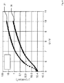
- is a graphical representation of current density in dependence on a voltage applied for a tandem organic light emitting device according to Example 1, for the tandem device comprising as the p-dopant in the p-CGL compound PD-3, in comparison with the device comprising a state-of-art p-dopant PD-1 (see Table 1);
- Fig. 5
- is a graphical representation of current density in dependence on a voltage applied for a tandem organic light emitting device according to Example 2, for the tandem device comprising as the p-dopant in the p-CGL compound PD-3, in comparison with the device comprising a state-of-art p-dopant PD-1 (see Table 2);
- Fig. 6
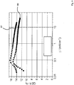
- is a graphical representation of quantum efficiency in dependence on current density for the tandem organic light emitting devices according to description for
Fig. 5 ; - Fig. 7
- is a graphical representation of current density in dependence on a voltage applied for a tandem organic light emitting device according to Example 3, for the tandem device comprising as the p-dopant in the p-CGL compound PD-3, in comparison with the device comprising a state-of-art p-dopant PD-1 (see Table 3); and
- Fig. 8
- is a graphical representation of quantum efficiency in dependence on current density for the tandem organic light emitting devices according to description for
Fig. 7 . -
Fig. 1 shows a schematic representation of a tandem organic light emitting device (tandem OLED). A stack oflayers 1 provided on asubstrate 2 comprises afirst electrode 3, and asecond electrode 4 provided as an anode and a cathode, respectively, in the embodiment depicted. - There is a charge generation layer, also named CGL, 5 provided comprising a n-
type sub-layer 5a, and a p-type sub-layer 5b. - A first
hole injection layer 6, a firsthole transport layer 7, and a firstelectron blocking layer 8 are provided between theanode 3 and a first emittinglayer 9. A firstelectron transport layer 10 is provided between the first emittinglayer 9 and thecharge generation layer 5. A secondhole injection layer 11, secondhole transport layer 12, and secondelectron blocking layer 13 are provided between thecharge generation layer 5 and a second emittinglayer 14. A secondelectron transport layer 15 is provided between the second emittinglayer 14 and thecathode 4. -
Fig. 2 shows a schematic representation of another tandem OLED. The stack oflayers 1 provided on thesubstrate 2, in addition, comprises aninterlayer 16. -
Fig. 3 shows a schematic representation of a further tandem OLED. In the stack oflayers 1 provided on thesubstrate 2 the n-type sublayer 5a of thecharge generation layer 5 comprises a first n-type sublayer 5a1 and a second n-type sublayer 5a2. In an alternative embodiment (not shown), thecharge generation layer 5 of the tandem OLED inFig. 5 may comprise theinterlayer 16. - Following, referring to graphical representation in
Fig. 4 to 8 , alternative embodiments of an organic electronic device provided as a tandem OLED are described which in general, in the examples discussed, are provided with a layer structure as shown inFig. 1 . The performance of the organic electronic devices comprising a p-type sub-layer comprising a fullerene compound comprising 48 fluorine groups, named C60F48 or PD-3, is compared to analogous organic electronic devices comprising state-of-art p-type sublayer comprising quinone compound PD-1. - For the different organic electronic devices, the performance has been studied compared to state of art p-dopants and p-dopants based on fullerenes comprising electron withdrawing groups in an organic electronic device provided as a tandem OLED.
- Following, an embodiment of a general procedure for fabrication of organic electronic devices is described.
- OLEDs with two emitting layers were prepared to demonstrate the technical benefit of an organic electronic device comprising a charge generation layer according to the present invention. As proof-of-concept, the tandem OLEDs comprised two blue emitting layers.
- A 15Ω /cm2 glass substrate with 90 nm ITO (available from Corning Co.) was cut to a size of 50 mm x 50 mm x 0.7 mm, ultrasonically cleaned with isopropyl alcohol for 5 minutes and then with pure water for 5 minutes, and cleaned again with UV ozone for 30 minutes, to prepare a first electrode.
- The organic layers are deposited sequentially on the ITO layer at 10-7 mbar, see Table 1 to 3 for compositions and layer thicknesses. In the Tables 1 to 3, c refers to the concentration, and d refers to the layer thickness.
- Then, the cathode electrode layer is formed by evaporating aluminum at ultra-high vacuum of 10-7 mbar and deposing the aluminum layer directly on the organic semiconductor layer. A thermal single co-evaporation of one or several metals is performed with a rate of 0, 1 to 10 nm/s (0.01 to 1 A/s) in order to generate a homogeneous cathode electrode with a thickness of 5 to 1000 nm. The thickness of the cathode electrode layer is 100 nm.
- The device is protected from ambient conditions by encapsulation of the device with a glass slide. Thereby, a cavity is formed, which comprises a getter material for further protection.
- To assess the performance of the inventive examples compared to the prior art, the current efficiency is measured under ambient conditions (20°C). Current voltage measurements are performed using a Keithley 2400 source meter, and recorded in V.
Table 1 - Example 1 Layer Layer material c / [vol%] d / [nm] anode ITO 100 90 first hole injection layer F1:PD-2 92:8 10 first hole transport layer F1 100 135 first electron blocking layer F2 100 10 first emitting layer ABH113: BD200 97:3 20 first electron transport layer F3: LiQ 50:50 25 n-type sub-layer F4 : Li 99:1 10 interlayer Metal (Li**) 100 0.5 p-type sub-layer F1:PD-1 or F1:PD-3 94.5:5.5* 10 80:20 10 second hole transport layer F1 100 35 second electron blocking layer F2 100 10 second emitting layer ABH113: BD200 97:3 20 second electron transport layer F3: LiQ 50:50 36 cathode Al 100 100 Table 2 - Example 2 Layer Layer material c [vol%] d [nm] anode ITO 100 90 first hole injection layer F1:PD-2 92:8 10 first hole transport layer F1 100 135 first electron blocking layer F2 100 10 first emitting layer ABH113: BD200 97:3 20 first electron transport layer F3: LiQ 50:50 25 first n-type sub-layer F4: Li 99:1 5 second n-type sub-layer F4 : Li from 90:10 to 80:20 5 p-type sub-layer F1:PD-1 or F1:PD-3 94.5:5.5* 10 80:20 10 second hole transport layer F1 100 35 second electron blocking layer F2 100 10 second emitting layer ABH113: BD200 97:3 20 second electron transport layer F3: LiQ 50:50 36 cathode Al 100 100 Table 3 - Example 3 Layer Layer material c [vol%] d [nm] anode ITO 100 90 first hole injection layer F1:PD-2 92:8 10 first hole transport layer F1 100 135 first electron blocking layer F2 100 10 first emitting layer ABH113: BD200 97:3 20 first electron transport layer F3 : LiQ 50:50 25 n-type sub-layer F4 : Yb 92:8 10 p-type sub-layer F1:PD-1 or F1:PD-3 94.5:5.5* 10 80:20 10 second hole transport layer F1 100 35 second electron blocking layer F2 100 10 second emitting layer ABH113: BD200 97:3 20 second electron transport layer F3: LiQ 50:50 36 cathode Al 100 100 * In the comparative examples, volume ratios matrix:p-dopant in the p-CGL were adjusted so that for both dopants, the molar ratio matrix:p-dopant was equal, having the same value 90:10.
** analogous devices comprising an Yb or Al interlayer afforded very similar results - Following, auxiliary materials were used in organic electronic devices according to Examples:


- ABH-113 is an emitter host and BD-200 is a blue fluorescent emitter dopant, both commercially available from SFC, Korea.
- Following, technical effects which may be provided by one or more of the alternative embodiments are described.
- In Example 1, an
interlayer 16 is provided between the n-type sub-layer 5a and the p-type sub-layer 5b of the charge generation layer 5 (seeFig. 2 ). The interlayer is provided with a layer thickness of about 1 nm. The interlayer is made of Li. The composition and thickness of all layers in example 1 can be taken from Table 1. The performance of the device is shown inFig. 4 . In this case, luminance measurement was made without calibration and quantitative efficiency evaluation was not made.Fig. 4 , however, shows a clear operating voltage benefit for fullerene compound PD-3 (curve 21) in comparison to quinone compound PD-1 (curve 20). - With regard to Example 2, the n-
type sub-layer 5a consists of two n-type sub-layers 5a1 and 5a2 having different redox n-dopant concentration (see Table 2). Li was used as redox n-dopant. The concentration of Li in the first n-type sublayer 5a1 is lower than the concentration of Li in the second n-type sub-layer 5a2. Thereby, a concentration gradient of Li achieved, whereby the concentration of Li in the n-type sub-layer closer to the first electrode is lower than the concentration of Li in the n-type sub-layer closer to the second electrode. The composition and thickness of all layers in example 2 can be taken from Table 2. -
Fig. 5 shows an operating voltage benefit for fullerene compound PD-3 (curve 31) in comparison to quinone compound PD-1 (curve 30). InFig. 6 , the results show comparable quantum efficiency for PD-1 (curve 40) and PD-3 (curve 41). - In example 3, the charge generation layer consists of a n-type sub-layer and a p-type sub-layer. The composition and thickness of all layers in example 3 can be taken from Table 3. In
Fig. 7 , it can be seen that fullerene compound PD-3 offers a benefit in operating voltage over quinone compound PD-1. Moreover,Fig. 6 shows a clear efficiency benefit of the use of fullerene compound PD-3 (curve 61) over the quinone compound PD-1 (curve 60) in this device arrangement. - The features disclosed in this specification, the figures and / or the claims may be material for the realization of various embodiments, taken in isolation or in various combinations thereof.
Claims (15)
- An organic electronic device, comprising- a first electrode (3);- a second electrode (4); and- a charge generation layer (5) arranged between the first and the second electrode (3, 4), the charge generation layer (5) comprising- a n-type sub-layer (5a) comprising at least one redox n-dopant and arranged closer to the first electrode, and- a p-type sub-layer (5b) comprising a fullerene compound dopant and arranged closer to the second electrode;wherein the fullerene compound comprises at least one electron withdrawing substituent selected from F, Cl, Br, I, CN, halogen-substituted and / or CN-substituted group containing 1 to 20 carbon atoms.
- The organic electronic device according to claim 1, wherein the at least one redox n-dopant is an elemental metal.
- The organic electronic device according to claim 1 or 2, wherein the fullerene compound comprises at least two electron withdrawing substituents independently selected from F and CN.
- The organic electronic device according to at least one of the preceding claims, wherein the fullerene compound has formula CxFy, wherein x is an integer from 60 to 120 and F is an integer equal or higher than x / 2.
- The organic electronic device according to at least one of the preceding claims, wherein the charge generation layer is provided with at least one of the following:- the n-type sub-layer (5a) comprises at least one electron transport matrix compound; and- the p-type sub-layer (5b) comprises at least one hole transport matrix compound.
- The organic electronic device according to claim 5, wherein the at least one hole transport matrix compound is an organic compound.
- The organic electronic device according to claim 5 or 6, wherein the at least one electron transport matrix compound is an organic compound.
- The organic electronic device according to at least one of the preceding claims, wherein- the n-type sub-layer (5a) comprises- a first n-type sub-layer (5a1) arranged closer to the first electrode (3), and- a second n-type sub-layer (5a2) arranged closer to the second electrode (4), and- the at least one redox n-dopant is provided with a higher concentration in the second n-type sub-layer (5a2) than in the first n-type sub-layer (5a1).
- The organic electronic device according to at least one of the preceding claims, wherein an interlayer (16) is provided between the n-type sub-layer (5a), and the p-type sub-layer (5b) in the charge generation layer (5).
- The organic electronic device according to at least one of the preceding claims, wherein- the first electrode (3) is provided as an anode;- the second electrode (4) is provided as a cathode;- the n-type sub-layer (5a) is arranged closer to the first electrode (3); and- the p-type sub-layer (5b) is arranged closer to the second electrode (4).
- The organic electronic device according to claim 10, comprising- at least one first light emitting layer (9) arranged between the first electrode (3) and the n-type sub-layer (5a), and- at least one second light emitting layer (14) arranged between the p-type sub-layer (5b) and the second electrode (4).
- The organic electronic device according to claim 10 or 11, wherein at least one of the at least one first light emitting layer (9) or the at least one second light emitting layer (14) comprises a blue emitter.
- The organic electronic device according to claim 12, wherein the blue emitter is a blue fluorescent emitter.
- A method for producing an organic electronic device comprising- a first electrode (3);- a second electrode (4); and- a charge generation layer (5) arranged between the first and the second electrode (3, 4), the charge generation layer (5) comprising- a n-type sub-layer (5a) comprising at least one redox n-dopant, and- a p-type sub-layer (5b) comprising a fullerene compound;wherein the fullerene compound comprises at least one electron withdrawing substituent selected from F, Cl, Br, I, CN, halogen-substituted and / or CN-substituted group containing 1 to 20 carbon atoms,
the method further comprising the steps of- providing a substrate (2) and the first electrode (3),- depositing a plurality of layers arranged on the first electrode (3), the plurality of layers comprising the charge generation layer (5), and- depositing the second electrode on the plurality of layers. - Method according to claim 14, wherein the depositing of the plurality of layers comprises a step of depositing the p-type sub-layer (5b), the depositing comprising evaporation and deposition of the fullerene compound under reduced pressure.
Priority Applications (2)
| Application Number | Priority Date | Filing Date | Title |
|---|---|---|---|
| EP17000963.3A EP3410510B1 (en) | 2017-06-02 | 2017-06-02 | Organic electronic device and method for producing the organic electronic device |
| PCT/EP2018/064541 WO2018220218A1 (en) | 2017-06-02 | 2018-06-02 | Organic electronic device and method for producing the organic electronic device |
Applications Claiming Priority (1)
| Application Number | Priority Date | Filing Date | Title |
|---|---|---|---|
| EP17000963.3A EP3410510B1 (en) | 2017-06-02 | 2017-06-02 | Organic electronic device and method for producing the organic electronic device |
Publications (2)
| Publication Number | Publication Date |
|---|---|
| EP3410510A1 true EP3410510A1 (en) | 2018-12-05 |
| EP3410510B1 EP3410510B1 (en) | 2021-10-20 |
Family
ID=59101244
Family Applications (1)
| Application Number | Title | Priority Date | Filing Date |
|---|---|---|---|
| EP17000963.3A Active EP3410510B1 (en) | 2017-06-02 | 2017-06-02 | Organic electronic device and method for producing the organic electronic device |
Country Status (2)
| Country | Link |
|---|---|
| EP (1) | EP3410510B1 (en) |
| WO (1) | WO2018220218A1 (en) |
Cited By (1)
| Publication number | Priority date | Publication date | Assignee | Title |
|---|---|---|---|---|
| EP4387414A1 (en) * | 2022-12-12 | 2024-06-19 | Novaled GmbH | Organic electroluminescent device comprising a compound of formula (i) and a compound of formula (ii), and display device comprising the organic electroluminescent device |
Families Citing this family (1)
| Publication number | Priority date | Publication date | Assignee | Title |
|---|---|---|---|---|
| CN118284097A (en) * | 2022-12-30 | 2024-07-02 | Tcl科技集团股份有限公司 | Light emitting device and method for manufacturing the same, and display device |
Citations (5)
| Publication number | Priority date | Publication date | Assignee | Title |
|---|---|---|---|---|
| WO2010029542A1 (en) | 2008-09-09 | 2010-03-18 | Technion Research & Development Foundation Ltd. | Derivatized fullerene-based dopants for organic semiconductors |
| WO2011154131A1 (en) | 2010-06-10 | 2011-12-15 | Novaled Ag | Electronic device comprising an organic semiconducting material |
| EP2833429A1 (en) | 2012-03-29 | 2015-02-04 | Sony Corporation | Organic electroluminescence element |
| US20160005991A1 (en) * | 2014-07-02 | 2016-01-07 | Samsung Display Co., Ltd. | Organic light-emitting device |
| WO2017089399A1 (en) | 2015-11-23 | 2017-06-01 | Novaled Gmbh | Organic semiconductive layer comprising phosphine oxide compounds |
-
2017
- 2017-06-02 EP EP17000963.3A patent/EP3410510B1/en active Active
-
2018
- 2018-06-02 WO PCT/EP2018/064541 patent/WO2018220218A1/en not_active Ceased
Patent Citations (6)
| Publication number | Priority date | Publication date | Assignee | Title |
|---|---|---|---|---|
| WO2010029542A1 (en) | 2008-09-09 | 2010-03-18 | Technion Research & Development Foundation Ltd. | Derivatized fullerene-based dopants for organic semiconductors |
| US20110156019A1 (en) * | 2008-09-09 | 2011-06-30 | Technion Research & Development Foundation, Ltd. | Derivatized fullerene-based dopants for organic semiconductors |
| WO2011154131A1 (en) | 2010-06-10 | 2011-12-15 | Novaled Ag | Electronic device comprising an organic semiconducting material |
| EP2833429A1 (en) | 2012-03-29 | 2015-02-04 | Sony Corporation | Organic electroluminescence element |
| US20160005991A1 (en) * | 2014-07-02 | 2016-01-07 | Samsung Display Co., Ltd. | Organic light-emitting device |
| WO2017089399A1 (en) | 2015-11-23 | 2017-06-01 | Novaled Gmbh | Organic semiconductive layer comprising phosphine oxide compounds |
Non-Patent Citations (1)
| Title |
|---|
| FENGYING LI ET AL: "Photoconductivity of [60]fullerene derivative doped PVK", SOLID STATE COMMUNICATIONS, vol. 107, no. 4, 1 January 1998 (1998-01-01), pages 189 - 192, XP055120493, ISSN: 0038-1098, DOI: 10.1016/S0038-1098(98)00187-2 * |
Cited By (2)
| Publication number | Priority date | Publication date | Assignee | Title |
|---|---|---|---|---|
| EP4387414A1 (en) * | 2022-12-12 | 2024-06-19 | Novaled GmbH | Organic electroluminescent device comprising a compound of formula (i) and a compound of formula (ii), and display device comprising the organic electroluminescent device |
| WO2024126528A1 (en) * | 2022-12-12 | 2024-06-20 | Novaled Gmbh | Organic electroluminescent device comprising a compound of formula (i) and a compound of formula (ii), and display device comprising the organic electroluminescent device |
Also Published As
| Publication number | Publication date |
|---|---|
| EP3410510B1 (en) | 2021-10-20 |
| WO2018220218A1 (en) | 2018-12-06 |
Similar Documents
| Publication | Publication Date | Title |
|---|---|---|
| EP3689867B1 (en) | Composition, organic semiconductor layer and electronic device | |
| EP3312899B1 (en) | Electron transport layer stack for an organic light-emitting diode | |
| US7830089B2 (en) | Electronic device with a layer structure of organic layers | |
| EP3425692B1 (en) | Organic electroluminescent device comprising an electron injection layer with zero-valent metal | |
| JP2024522490A (en) | Sheet resistance parts | |
| EP3503240B1 (en) | Organic semiconductor layer | |
| EP4284780B1 (en) | Organic compound of formula (i) for use in organic electronic devices, an organic electronic device comprising a compound of formula (i) and a display device comprising the organic electronic device | |
| US20190322642A1 (en) | Compound and Organic Semiconducting Layer, Organic Electronic Device, Display Device and Lighting Device Comprising the Same | |
| US20230240132A1 (en) | Organic Electronic Device Comprising a Compound of Formula (1), Display Device Comprising the Organic Electronic Device as Well as Compounds of Formula (1) for Use in Organic Electronic Devices | |
| EP3369729B1 (en) | Fused 9-phenyl-acridine derivatives for use in an electronic device and display device | |
| WO2020074379A1 (en) | Organic light emitting device | |
| EP3483157B1 (en) | Compounds comprising triazine group, fluorene-group and hetero-fluorene group | |
| KR102890885B1 (en) | Organic EL devices | |
| EP3410510B1 (en) | Organic electronic device and method for producing the organic electronic device | |
| EP3374538B1 (en) | Process for making a metal containing layer | |
| WO2007071450A1 (en) | Electronic device with a layer structure of organic layers | |
| EP3527557A1 (en) | N-heteroarylene compounds | |
| KR102731961B1 (en) | A metallic layer comprising an alkali metal and a second metal | |
| EP3483153B1 (en) | Compounds comprising triazine group, fluorene-group and aryl group and their use in organic electronic devices | |
| CN117561811B (en) | Organic electronic devices comprising metal compounds containing metal cations and at least one borate anion of formula (I), their uses and methods of preparation | |
| US20240292655A1 (en) | Sheet resistance component | |
| Chen et al. | Investigations of electron-injection mechanisms and interfacial chemical reactions of Bphen doped with rubidium carbonate in OLEDs | |
| WO2025125148A1 (en) | Organic electroluminescent device and display device |
Legal Events
| Date | Code | Title | Description |
|---|---|---|---|
| PUAI | Public reference made under article 153(3) epc to a published international application that has entered the european phase |
Free format text: ORIGINAL CODE: 0009012 |
|
| STAA | Information on the status of an ep patent application or granted ep patent |
Free format text: STATUS: THE APPLICATION HAS BEEN PUBLISHED |
|
| AK | Designated contracting states |
Kind code of ref document: A1 Designated state(s): AL AT BE BG CH CY CZ DE DK EE ES FI FR GB GR HR HU IE IS IT LI LT LU LV MC MK MT NL NO PL PT RO RS SE SI SK SM TR |
|
| AX | Request for extension of the european patent |
Extension state: BA ME |
|
| STAA | Information on the status of an ep patent application or granted ep patent |
Free format text: STATUS: REQUEST FOR EXAMINATION WAS MADE |
|
| RAP1 | Party data changed (applicant data changed or rights of an application transferred) |
Owner name: NOVALED GMBH |
|
| 17P | Request for examination filed |
Effective date: 20190605 |
|
| RBV | Designated contracting states (corrected) |
Designated state(s): AL AT BE BG CH CY CZ DE DK EE ES FI FR GB GR HR HU IE IS IT LI LT LU LV MC MK MT NL NO PL PT RO RS SE SI SK SM TR |
|
| STAA | Information on the status of an ep patent application or granted ep patent |
Free format text: STATUS: EXAMINATION IS IN PROGRESS |
|
| 17Q | First examination report despatched |
Effective date: 20200330 |
|
| GRAP | Despatch of communication of intention to grant a patent |
Free format text: ORIGINAL CODE: EPIDOSNIGR1 |
|
| STAA | Information on the status of an ep patent application or granted ep patent |
Free format text: STATUS: GRANT OF PATENT IS INTENDED |
|
| INTG | Intention to grant announced |
Effective date: 20210602 |
|
| GRAS | Grant fee paid |
Free format text: ORIGINAL CODE: EPIDOSNIGR3 |
|
| GRAA | (expected) grant |
Free format text: ORIGINAL CODE: 0009210 |
|
| STAA | Information on the status of an ep patent application or granted ep patent |
Free format text: STATUS: THE PATENT HAS BEEN GRANTED |
|
| AK | Designated contracting states |
Kind code of ref document: B1 Designated state(s): AL AT BE BG CH CY CZ DE DK EE ES FI FR GB GR HR HU IE IS IT LI LT LU LV MC MK MT NL NO PL PT RO RS SE SI SK SM TR |
|
| REG | Reference to a national code |
Ref country code: GB Ref legal event code: FG4D |
|
| REG | Reference to a national code |
Ref country code: CH Ref legal event code: EP |
|
| REG | Reference to a national code |
Ref country code: IE Ref legal event code: FG4D |
|
| REG | Reference to a national code |
Ref country code: DE Ref legal event code: R096 Ref document number: 602017047773 Country of ref document: DE |
|
| REG | Reference to a national code |
Ref country code: AT Ref legal event code: REF Ref document number: 1440653 Country of ref document: AT Kind code of ref document: T Effective date: 20211115 |
|
| REG | Reference to a national code |
Ref country code: LT Ref legal event code: MG9D |
|
| REG | Reference to a national code |
Ref country code: NL Ref legal event code: MP Effective date: 20211020 |
|
| REG | Reference to a national code |
Ref country code: AT Ref legal event code: MK05 Ref document number: 1440653 Country of ref document: AT Kind code of ref document: T Effective date: 20211020 |
|
| PG25 | Lapsed in a contracting state [announced via postgrant information from national office to epo] |
Ref country code: RS Free format text: LAPSE BECAUSE OF FAILURE TO SUBMIT A TRANSLATION OF THE DESCRIPTION OR TO PAY THE FEE WITHIN THE PRESCRIBED TIME-LIMIT Effective date: 20211020 Ref country code: LT Free format text: LAPSE BECAUSE OF FAILURE TO SUBMIT A TRANSLATION OF THE DESCRIPTION OR TO PAY THE FEE WITHIN THE PRESCRIBED TIME-LIMIT Effective date: 20211020 Ref country code: FI Free format text: LAPSE BECAUSE OF FAILURE TO SUBMIT A TRANSLATION OF THE DESCRIPTION OR TO PAY THE FEE WITHIN THE PRESCRIBED TIME-LIMIT Effective date: 20211020 Ref country code: BG Free format text: LAPSE BECAUSE OF FAILURE TO SUBMIT A TRANSLATION OF THE DESCRIPTION OR TO PAY THE FEE WITHIN THE PRESCRIBED TIME-LIMIT Effective date: 20220120 Ref country code: AT Free format text: LAPSE BECAUSE OF FAILURE TO SUBMIT A TRANSLATION OF THE DESCRIPTION OR TO PAY THE FEE WITHIN THE PRESCRIBED TIME-LIMIT Effective date: 20211020 |
|
| PG25 | Lapsed in a contracting state [announced via postgrant information from national office to epo] |
Ref country code: IS Free format text: LAPSE BECAUSE OF FAILURE TO SUBMIT A TRANSLATION OF THE DESCRIPTION OR TO PAY THE FEE WITHIN THE PRESCRIBED TIME-LIMIT Effective date: 20220220 Ref country code: SE Free format text: LAPSE BECAUSE OF FAILURE TO SUBMIT A TRANSLATION OF THE DESCRIPTION OR TO PAY THE FEE WITHIN THE PRESCRIBED TIME-LIMIT Effective date: 20211020 Ref country code: PT Free format text: LAPSE BECAUSE OF FAILURE TO SUBMIT A TRANSLATION OF THE DESCRIPTION OR TO PAY THE FEE WITHIN THE PRESCRIBED TIME-LIMIT Effective date: 20220221 Ref country code: PL Free format text: LAPSE BECAUSE OF FAILURE TO SUBMIT A TRANSLATION OF THE DESCRIPTION OR TO PAY THE FEE WITHIN THE PRESCRIBED TIME-LIMIT Effective date: 20211020 Ref country code: NO Free format text: LAPSE BECAUSE OF FAILURE TO SUBMIT A TRANSLATION OF THE DESCRIPTION OR TO PAY THE FEE WITHIN THE PRESCRIBED TIME-LIMIT Effective date: 20220120 Ref country code: NL Free format text: LAPSE BECAUSE OF FAILURE TO SUBMIT A TRANSLATION OF THE DESCRIPTION OR TO PAY THE FEE WITHIN THE PRESCRIBED TIME-LIMIT Effective date: 20211020 Ref country code: LV Free format text: LAPSE BECAUSE OF FAILURE TO SUBMIT A TRANSLATION OF THE DESCRIPTION OR TO PAY THE FEE WITHIN THE PRESCRIBED TIME-LIMIT Effective date: 20211020 Ref country code: HR Free format text: LAPSE BECAUSE OF FAILURE TO SUBMIT A TRANSLATION OF THE DESCRIPTION OR TO PAY THE FEE WITHIN THE PRESCRIBED TIME-LIMIT Effective date: 20211020 Ref country code: GR Free format text: LAPSE BECAUSE OF FAILURE TO SUBMIT A TRANSLATION OF THE DESCRIPTION OR TO PAY THE FEE WITHIN THE PRESCRIBED TIME-LIMIT Effective date: 20220121 Ref country code: ES Free format text: LAPSE BECAUSE OF FAILURE TO SUBMIT A TRANSLATION OF THE DESCRIPTION OR TO PAY THE FEE WITHIN THE PRESCRIBED TIME-LIMIT Effective date: 20211020 |
|
| REG | Reference to a national code |
Ref country code: DE Ref legal event code: R097 Ref document number: 602017047773 Country of ref document: DE |
|
| PG25 | Lapsed in a contracting state [announced via postgrant information from national office to epo] |
Ref country code: SM Free format text: LAPSE BECAUSE OF FAILURE TO SUBMIT A TRANSLATION OF THE DESCRIPTION OR TO PAY THE FEE WITHIN THE PRESCRIBED TIME-LIMIT Effective date: 20211020 Ref country code: SK Free format text: LAPSE BECAUSE OF FAILURE TO SUBMIT A TRANSLATION OF THE DESCRIPTION OR TO PAY THE FEE WITHIN THE PRESCRIBED TIME-LIMIT Effective date: 20211020 Ref country code: RO Free format text: LAPSE BECAUSE OF FAILURE TO SUBMIT A TRANSLATION OF THE DESCRIPTION OR TO PAY THE FEE WITHIN THE PRESCRIBED TIME-LIMIT Effective date: 20211020 Ref country code: EE Free format text: LAPSE BECAUSE OF FAILURE TO SUBMIT A TRANSLATION OF THE DESCRIPTION OR TO PAY THE FEE WITHIN THE PRESCRIBED TIME-LIMIT Effective date: 20211020 Ref country code: DK Free format text: LAPSE BECAUSE OF FAILURE TO SUBMIT A TRANSLATION OF THE DESCRIPTION OR TO PAY THE FEE WITHIN THE PRESCRIBED TIME-LIMIT Effective date: 20211020 Ref country code: CZ Free format text: LAPSE BECAUSE OF FAILURE TO SUBMIT A TRANSLATION OF THE DESCRIPTION OR TO PAY THE FEE WITHIN THE PRESCRIBED TIME-LIMIT Effective date: 20211020 |
|
| PLBE | No opposition filed within time limit |
Free format text: ORIGINAL CODE: 0009261 |
|
| STAA | Information on the status of an ep patent application or granted ep patent |
Free format text: STATUS: NO OPPOSITION FILED WITHIN TIME LIMIT |
|
| 26N | No opposition filed |
Effective date: 20220721 |
|
| PG25 | Lapsed in a contracting state [announced via postgrant information from national office to epo] |
Ref country code: AL Free format text: LAPSE BECAUSE OF FAILURE TO SUBMIT A TRANSLATION OF THE DESCRIPTION OR TO PAY THE FEE WITHIN THE PRESCRIBED TIME-LIMIT Effective date: 20211020 |
|
| REG | Reference to a national code |
Ref country code: DE Ref legal event code: R079 Ref document number: 602017047773 Country of ref document: DE Free format text: PREVIOUS MAIN CLASS: H01L0051540000 Ipc: H10K0085000000 |
|
| PG25 | Lapsed in a contracting state [announced via postgrant information from national office to epo] |
Ref country code: SI Free format text: LAPSE BECAUSE OF FAILURE TO SUBMIT A TRANSLATION OF THE DESCRIPTION OR TO PAY THE FEE WITHIN THE PRESCRIBED TIME-LIMIT Effective date: 20211020 |
|
| PG25 | Lapsed in a contracting state [announced via postgrant information from national office to epo] |
Ref country code: MC Free format text: LAPSE BECAUSE OF FAILURE TO SUBMIT A TRANSLATION OF THE DESCRIPTION OR TO PAY THE FEE WITHIN THE PRESCRIBED TIME-LIMIT Effective date: 20211020 |
|
| REG | Reference to a national code |
Ref country code: CH Ref legal event code: PL |
|
| REG | Reference to a national code |
Ref country code: BE Ref legal event code: MM Effective date: 20220630 |
|
| GBPC | Gb: european patent ceased through non-payment of renewal fee |
Effective date: 20220602 |
|
| PG25 | Lapsed in a contracting state [announced via postgrant information from national office to epo] |
Ref country code: LU Free format text: LAPSE BECAUSE OF NON-PAYMENT OF DUE FEES Effective date: 20220602 Ref country code: LI Free format text: LAPSE BECAUSE OF NON-PAYMENT OF DUE FEES Effective date: 20220630 Ref country code: IE Free format text: LAPSE BECAUSE OF NON-PAYMENT OF DUE FEES Effective date: 20220602 Ref country code: FR Free format text: LAPSE BECAUSE OF NON-PAYMENT OF DUE FEES Effective date: 20220630 Ref country code: CH Free format text: LAPSE BECAUSE OF NON-PAYMENT OF DUE FEES Effective date: 20220630 |
|
| PG25 | Lapsed in a contracting state [announced via postgrant information from national office to epo] |
Ref country code: IT Free format text: LAPSE BECAUSE OF FAILURE TO SUBMIT A TRANSLATION OF THE DESCRIPTION OR TO PAY THE FEE WITHIN THE PRESCRIBED TIME-LIMIT Effective date: 20211020 Ref country code: GB Free format text: LAPSE BECAUSE OF NON-PAYMENT OF DUE FEES Effective date: 20220602 Ref country code: BE Free format text: LAPSE BECAUSE OF NON-PAYMENT OF DUE FEES Effective date: 20220630 |
|
| P01 | Opt-out of the competence of the unified patent court (upc) registered |
Effective date: 20230515 |
|
| PG25 | Lapsed in a contracting state [announced via postgrant information from national office to epo] |
Ref country code: HU Free format text: LAPSE BECAUSE OF FAILURE TO SUBMIT A TRANSLATION OF THE DESCRIPTION OR TO PAY THE FEE WITHIN THE PRESCRIBED TIME-LIMIT; INVALID AB INITIO Effective date: 20170602 |
|
| PG25 | Lapsed in a contracting state [announced via postgrant information from national office to epo] |
Ref country code: MK Free format text: LAPSE BECAUSE OF FAILURE TO SUBMIT A TRANSLATION OF THE DESCRIPTION OR TO PAY THE FEE WITHIN THE PRESCRIBED TIME-LIMIT Effective date: 20211020 Ref country code: CY Free format text: LAPSE BECAUSE OF FAILURE TO SUBMIT A TRANSLATION OF THE DESCRIPTION OR TO PAY THE FEE WITHIN THE PRESCRIBED TIME-LIMIT Effective date: 20211020 |
|
| PG25 | Lapsed in a contracting state [announced via postgrant information from national office to epo] |
Ref country code: MT Free format text: LAPSE BECAUSE OF FAILURE TO SUBMIT A TRANSLATION OF THE DESCRIPTION OR TO PAY THE FEE WITHIN THE PRESCRIBED TIME-LIMIT Effective date: 20211020 |
|
| PG25 | Lapsed in a contracting state [announced via postgrant information from national office to epo] |
Ref country code: TR Free format text: LAPSE BECAUSE OF FAILURE TO SUBMIT A TRANSLATION OF THE DESCRIPTION OR TO PAY THE FEE WITHIN THE PRESCRIBED TIME-LIMIT Effective date: 20211020 |
|
| PGFP | Annual fee paid to national office [announced via postgrant information from national office to epo] |
Ref country code: DE Payment date: 20260331 Year of fee payment: 10 |