EP3410500A1 - Light emitting device, backlight device, and manufacturing method of light emitting device - Google Patents
Light emitting device, backlight device, and manufacturing method of light emitting device Download PDFInfo
- Publication number
- EP3410500A1 EP3410500A1 EP16888137.3A EP16888137A EP3410500A1 EP 3410500 A1 EP3410500 A1 EP 3410500A1 EP 16888137 A EP16888137 A EP 16888137A EP 3410500 A1 EP3410500 A1 EP 3410500A1
- Authority
- EP
- European Patent Office
- Prior art keywords
- light emitting
- emitting device
- electrode
- molded body
- resin molded
- Prior art date
- Legal status (The legal status is an assumption and is not a legal conclusion. Google has not performed a legal analysis and makes no representation as to the accuracy of the status listed.)
- Granted
Links
Images

Classifications
-
- H—ELECTRICITY
- H10—SEMICONDUCTOR DEVICES; ELECTRIC SOLID-STATE DEVICES NOT OTHERWISE PROVIDED FOR
- H10H—INORGANIC LIGHT-EMITTING SEMICONDUCTOR DEVICES HAVING POTENTIAL BARRIERS
- H10H20/00—Individual inorganic light-emitting semiconductor devices having potential barriers, e.g. light-emitting diodes [LED]
- H10H20/80—Constructional details
- H10H20/85—Packages
- H10H20/852—Encapsulations
- H10H20/853—Encapsulations characterised by their shape
-
- G—PHYSICS
- G02—OPTICS
- G02B—OPTICAL ELEMENTS, SYSTEMS OR APPARATUS
- G02B6/00—Light guides; Structural details of arrangements comprising light guides and other optical elements, e.g. couplings
- G02B6/0001—Light guides; Structural details of arrangements comprising light guides and other optical elements, e.g. couplings specially adapted for lighting devices or systems
- G02B6/0011—Light guides; Structural details of arrangements comprising light guides and other optical elements, e.g. couplings specially adapted for lighting devices or systems the light guides being planar or of plate-like form
- G02B6/0066—Light guides; Structural details of arrangements comprising light guides and other optical elements, e.g. couplings specially adapted for lighting devices or systems the light guides being planar or of plate-like form characterised by the light source being coupled to the light guide
- G02B6/0073—Light emitting diode [LED]
-
- G—PHYSICS
- G02—OPTICS
- G02B—OPTICAL ELEMENTS, SYSTEMS OR APPARATUS
- G02B6/00—Light guides; Structural details of arrangements comprising light guides and other optical elements, e.g. couplings
- G02B6/0001—Light guides; Structural details of arrangements comprising light guides and other optical elements, e.g. couplings specially adapted for lighting devices or systems
- G02B6/0011—Light guides; Structural details of arrangements comprising light guides and other optical elements, e.g. couplings specially adapted for lighting devices or systems the light guides being planar or of plate-like form
- G02B6/0081—Mechanical or electrical aspects of the light guide and light source in the lighting device peculiar to the adaptation to planar light guides, e.g. concerning packaging
- G02B6/0083—Details of electrical connections of light sources to drivers, circuit boards, or the like
-
- H—ELECTRICITY
- H10—SEMICONDUCTOR DEVICES; ELECTRIC SOLID-STATE DEVICES NOT OTHERWISE PROVIDED FOR
- H10H—INORGANIC LIGHT-EMITTING SEMICONDUCTOR DEVICES HAVING POTENTIAL BARRIERS
- H10H20/00—Individual inorganic light-emitting semiconductor devices having potential barriers, e.g. light-emitting diodes [LED]
- H10H20/01—Manufacture or treatment
- H10H20/011—Manufacture or treatment of bodies, e.g. forming semiconductor layers
- H10H20/018—Bonding of wafers
-
- H—ELECTRICITY
- H10—SEMICONDUCTOR DEVICES; ELECTRIC SOLID-STATE DEVICES NOT OTHERWISE PROVIDED FOR
- H10H—INORGANIC LIGHT-EMITTING SEMICONDUCTOR DEVICES HAVING POTENTIAL BARRIERS
- H10H20/00—Individual inorganic light-emitting semiconductor devices having potential barriers, e.g. light-emitting diodes [LED]
- H10H20/80—Constructional details
- H10H20/83—Electrodes
-
- H—ELECTRICITY
- H10—SEMICONDUCTOR DEVICES; ELECTRIC SOLID-STATE DEVICES NOT OTHERWISE PROVIDED FOR
- H10H—INORGANIC LIGHT-EMITTING SEMICONDUCTOR DEVICES HAVING POTENTIAL BARRIERS
- H10H20/00—Individual inorganic light-emitting semiconductor devices having potential barriers, e.g. light-emitting diodes [LED]
- H10H20/80—Constructional details
- H10H20/85—Packages
- H10H20/857—Interconnections, e.g. lead-frames, bond wires or solder balls
-
- H—ELECTRICITY
- H10—SEMICONDUCTOR DEVICES; ELECTRIC SOLID-STATE DEVICES NOT OTHERWISE PROVIDED FOR
- H10W—GENERIC PACKAGES, INTERCONNECTIONS, CONNECTORS OR OTHER CONSTRUCTIONAL DETAILS OF DEVICES COVERED BY CLASS H10
- H10W90/00—Package configurations
-
- G—PHYSICS
- G02—OPTICS
- G02B—OPTICAL ELEMENTS, SYSTEMS OR APPARATUS
- G02B6/00—Light guides; Structural details of arrangements comprising light guides and other optical elements, e.g. couplings
- G02B6/0001—Light guides; Structural details of arrangements comprising light guides and other optical elements, e.g. couplings specially adapted for lighting devices or systems
- G02B6/0011—Light guides; Structural details of arrangements comprising light guides and other optical elements, e.g. couplings specially adapted for lighting devices or systems the light guides being planar or of plate-like form
- G02B6/0066—Light guides; Structural details of arrangements comprising light guides and other optical elements, e.g. couplings specially adapted for lighting devices or systems the light guides being planar or of plate-like form characterised by the light source being coupled to the light guide
- G02B6/0068—Arrangements of plural sources, e.g. multi-colour light sources
-
- G—PHYSICS
- G02—OPTICS
- G02B—OPTICAL ELEMENTS, SYSTEMS OR APPARATUS
- G02B6/00—Light guides; Structural details of arrangements comprising light guides and other optical elements, e.g. couplings
- G02B6/0001—Light guides; Structural details of arrangements comprising light guides and other optical elements, e.g. couplings specially adapted for lighting devices or systems
- G02B6/0011—Light guides; Structural details of arrangements comprising light guides and other optical elements, e.g. couplings specially adapted for lighting devices or systems the light guides being planar or of plate-like form
- G02B6/0081—Mechanical or electrical aspects of the light guide and light source in the lighting device peculiar to the adaptation to planar light guides, e.g. concerning packaging
- G02B6/0086—Positioning aspects
- G02B6/009—Positioning aspects of the light source in the package
-
- H—ELECTRICITY
- H10—SEMICONDUCTOR DEVICES; ELECTRIC SOLID-STATE DEVICES NOT OTHERWISE PROVIDED FOR
- H10H—INORGANIC LIGHT-EMITTING SEMICONDUCTOR DEVICES HAVING POTENTIAL BARRIERS
- H10H20/00—Individual inorganic light-emitting semiconductor devices having potential barriers, e.g. light-emitting diodes [LED]
- H10H20/01—Manufacture or treatment
- H10H20/036—Manufacture or treatment of packages
- H10H20/0362—Manufacture or treatment of packages of encapsulations
-
- H—ELECTRICITY
- H10—SEMICONDUCTOR DEVICES; ELECTRIC SOLID-STATE DEVICES NOT OTHERWISE PROVIDED FOR
- H10H—INORGANIC LIGHT-EMITTING SEMICONDUCTOR DEVICES HAVING POTENTIAL BARRIERS
- H10H20/00—Individual inorganic light-emitting semiconductor devices having potential barriers, e.g. light-emitting diodes [LED]
- H10H20/01—Manufacture or treatment
- H10H20/036—Manufacture or treatment of packages
- H10H20/0364—Manufacture or treatment of packages of interconnections
-
- H—ELECTRICITY
- H10—SEMICONDUCTOR DEVICES; ELECTRIC SOLID-STATE DEVICES NOT OTHERWISE PROVIDED FOR
- H10H—INORGANIC LIGHT-EMITTING SEMICONDUCTOR DEVICES HAVING POTENTIAL BARRIERS
- H10H20/00—Individual inorganic light-emitting semiconductor devices having potential barriers, e.g. light-emitting diodes [LED]
- H10H20/80—Constructional details
- H10H20/85—Packages
- H10H20/8506—Containers
-
- H—ELECTRICITY
- H10—SEMICONDUCTOR DEVICES; ELECTRIC SOLID-STATE DEVICES NOT OTHERWISE PROVIDED FOR
- H10H—INORGANIC LIGHT-EMITTING SEMICONDUCTOR DEVICES HAVING POTENTIAL BARRIERS
- H10H20/00—Individual inorganic light-emitting semiconductor devices having potential barriers, e.g. light-emitting diodes [LED]
- H10H20/80—Constructional details
- H10H20/85—Packages
- H10H20/852—Encapsulations
- H10H20/854—Encapsulations characterised by their material, e.g. epoxy or silicone resins
-
- H—ELECTRICITY
- H10—SEMICONDUCTOR DEVICES; ELECTRIC SOLID-STATE DEVICES NOT OTHERWISE PROVIDED FOR
- H10K—ORGANIC ELECTRIC SOLID-STATE DEVICES
- H10K71/00—Manufacture or treatment specially adapted for the organic devices covered by this subclass
-
- H—ELECTRICITY
- H10—SEMICONDUCTOR DEVICES; ELECTRIC SOLID-STATE DEVICES NOT OTHERWISE PROVIDED FOR
- H10W—GENERIC PACKAGES, INTERCONNECTIONS, CONNECTORS OR OTHER CONSTRUCTIONAL DETAILS OF DEVICES COVERED BY CLASS H10
- H10W70/00—Package substrates; Interposers; Redistribution layers [RDL]
- H10W70/60—Insulating or insulated package substrates; Interposers; Redistribution layers
-
- H—ELECTRICITY
- H10—SEMICONDUCTOR DEVICES; ELECTRIC SOLID-STATE DEVICES NOT OTHERWISE PROVIDED FOR
- H10W—GENERIC PACKAGES, INTERCONNECTIONS, CONNECTORS OR OTHER CONSTRUCTIONAL DETAILS OF DEVICES COVERED BY CLASS H10
- H10W72/00—Interconnections or connectors in packages
- H10W72/01—Manufacture or treatment
- H10W72/0198—Manufacture or treatment batch processes
-
- H—ELECTRICITY
- H10—SEMICONDUCTOR DEVICES; ELECTRIC SOLID-STATE DEVICES NOT OTHERWISE PROVIDED FOR
- H10W—GENERIC PACKAGES, INTERCONNECTIONS, CONNECTORS OR OTHER CONSTRUCTIONAL DETAILS OF DEVICES COVERED BY CLASS H10
- H10W72/00—Interconnections or connectors in packages
- H10W72/90—Bond pads, in general
- H10W72/941—Dispositions of bond pads
- H10W72/9413—Dispositions of bond pads on encapsulations
-
- H—ELECTRICITY
- H10—SEMICONDUCTOR DEVICES; ELECTRIC SOLID-STATE DEVICES NOT OTHERWISE PROVIDED FOR
- H10W—GENERIC PACKAGES, INTERCONNECTIONS, CONNECTORS OR OTHER CONSTRUCTIONAL DETAILS OF DEVICES COVERED BY CLASS H10
- H10W72/00—Interconnections or connectors in packages
- H10W72/90—Bond pads, in general
- H10W72/941—Dispositions of bond pads
- H10W72/944—Dispositions of multiple bond pads
-
- H—ELECTRICITY
- H10—SEMICONDUCTOR DEVICES; ELECTRIC SOLID-STATE DEVICES NOT OTHERWISE PROVIDED FOR
- H10W—GENERIC PACKAGES, INTERCONNECTIONS, CONNECTORS OR OTHER CONSTRUCTIONAL DETAILS OF DEVICES COVERED BY CLASS H10
- H10W74/00—Encapsulations, e.g. protective coatings
- H10W74/10—Encapsulations, e.g. protective coatings characterised by their shape or disposition
- H10W74/131—Encapsulations, e.g. protective coatings characterised by their shape or disposition the semiconductor body being only partially enclosed
- H10W74/142—Encapsulations, e.g. protective coatings characterised by their shape or disposition the semiconductor body being only partially enclosed the encapsulations exposing the passive side of the semiconductor body
-
- H—ELECTRICITY
- H10—SEMICONDUCTOR DEVICES; ELECTRIC SOLID-STATE DEVICES NOT OTHERWISE PROVIDED FOR
- H10W—GENERIC PACKAGES, INTERCONNECTIONS, CONNECTORS OR OTHER CONSTRUCTIONAL DETAILS OF DEVICES COVERED BY CLASS H10
- H10W90/00—Package configurations
- H10W90/10—Configurations of laterally-adjacent chips
-
- H—ELECTRICITY
- H10—SEMICONDUCTOR DEVICES; ELECTRIC SOLID-STATE DEVICES NOT OTHERWISE PROVIDED FOR
- H10W—GENERIC PACKAGES, INTERCONNECTIONS, CONNECTORS OR OTHER CONSTRUCTIONAL DETAILS OF DEVICES COVERED BY CLASS H10
- H10W90/00—Package configurations
- H10W90/701—Package configurations characterised by the relative positions of pads or connectors relative to package parts
- H10W90/721—Package configurations characterised by the relative positions of pads or connectors relative to package parts of bump connectors
- H10W90/724—Package configurations characterised by the relative positions of pads or connectors relative to package parts of bump connectors between a chip and a stacked insulating package substrate, interposer or RDL
Definitions
- the present invention relates to a light emitting device including light emitting elements such as light emitting diode (LED) elements.
- LED light emitting diode
- a backlight including a plurality of light emitting diode (LED) elements is generally used as an electronic component configured to illuminate a liquid crystal display from a back surface thereof.
- LED light emitting diode
- edge light type and direct type systems as such a backlight, and an edge light type is used for a small liquid crystal used for a portable terminal or the like, a laptop type personal computer, a liquid crystal monitor, and the like.
- an edge light type backlight a plurality of LED elements are arranged in any lateral surface of a plate-like light guide plate and the entire surface of a liquid crystal panel is irradiated with light through the light guide plate. Since the number of required LED elements is smaller in such a type than that of a direct type, the edge light type backlight has advantages such as low cost, energy saving, and a liquid crystal display which can be made thin.
- Fig. 7 is a diagram showing a configuration of a light emitting device 101 according to the related art.
- the light emitting device 101 includes a printed board 102 and a plurality of LED elements 103.
- each of the LED elements 103 includes a base part 131, a light emitting unit 132, a positive electrode 133, and a negative electrode 134.
- a wiring 121 is formed in a front surface of the printed board 102 using a method such as etching. Furthermore, the printed board 102 is assembled with a resin casing 105.
- the light emitting unit 132 constituted of a light emitting diode is provided in a first surface of the base part 131.
- the positive electrode 133 and the negative electrode 134 are provided in a second surface which is perpendicular to the first surface of the base part 131.
- the positive electrode 133 and the negative electrode 134 are connected to the wiring 121 using a solder material 122 to be mounted in the front surface of the printed board 102.
- a thickness of a printed board 101 since a thickness of a printed board 101, a thickness of the wiring 121, a floating thickness of a joint using the solder material 122, and a thickness of a space required for assembly of the printed board 102 and the resin casing 105 are required in a configuration in which the LED elements 103 are mounted in the front surface of the printed board 102, there is a problem in that a height (thickness in an H direction) of the light emitting device 101 is obtained by adding a thickness of at least about 0.1 mm to a thickness of the LED element 103.
- the light emitting device 101a of a configuration illustrated in Fig. 8 can be considered.
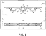
- Fig. 8 is a diagram showing a configuration of a light emitting device 101a according to the related art.
- the positive electrode 133 and the negative electrode 134 are provided in an opposite side to the light emitting unit 132 of the LED element 103 and connected to the wiring 121 in the printed board 102 via a solder material 104. Since a height (thickness in an H direction) of the printed board 102 is substantially the same as a height of the LED element 103 in such a configuration, a thickness of the light emitting device 101a can be made as thin as a thickness of the LED element 103.
- miniaturization of a light emitting device is required due to an increasing demand for miniaturization and thinning of electronic devices in recent years.
- the light emitting device 101 (101a) obtained through a mounting method using the solder material 122 in the related art it is necessary to secure an installation space of the solder material 122 in the light emitting device 101 (101a) in view of wet spreading of the solder material 122, securing a mounting strength, or the like. Therefore, there is a limit to miniaturization of the light emitting device 101 (101a).
- Patent Literature 1 discloses a method for fixing an LED mounting position by forming a groove in the LED mounting position in a printed board and inserting an LED member joined to a dummy having a dimension which is the same as a mounting pitch of an LED into the groove.
- Patent Literature 2 discloses a method for fixing an LED mounting position by putting an adhesive into a hole formed in a printed board, mounting an LED above the adhesive, and curing the adhesive.
- Patent Literature 3 discloses a method for fixing an LED mounting position by assembling an LED and a positioned member and then soldering the LED to a circuit of a printed board.
- an object of the present invention is to realize a light emitting device which is further miniaturized and thinned, a backlight device including such a light emitting device, and a manufacturing method for more easily manufacturing such a light emitting device.
- a light emitting device includes: a resin molded body; a light emitting element including at least a light emitting unit and an electrode and embedded in the resin molded body so that the light emitting unit is exposed on a first surface in the resin molded body and the electrode is exposed on a second surface which is perpendicular to the first surface in the resin molded body; and a wiring formed in the second surface in the resin molded body and connected to the electrode.
- a backlight device includes: a light guide plate; and the light emitting devices described above arranged to face any lateral surface of the light guide plate.
- a manufacturing method of a light emitting device includes: a step of temporarily fixing a light emitting element including at least a light emitting unit and an electrode formed in a surface which is perpendicular to a surface in which the light emitting unit is formed to a temporary fixing film in such a way that the electrode is in contact with the temporary fixing film; a step of forming a resin molded body in which the light emitting element is embedded by arranging the temporary fixing film in which the light emitting element is temporarily fixed in a gap in a mold and injecting a resin material into the gap; a step of peeling the temporary fixing film off the resin molded body; and a step of forming a wiring connected to the electrode in a surface on which the electrode in the resin molded body is exposed.
- a more compact and thinner light emitting device a backlight device including such a light emitting device, and a manufacturing method for more easily manufacturing such a light emitting device can be realized.
- Embodiment 1 of the present invention will be described below with reference to Figs. 1 and 2 .
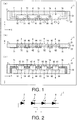
- Fig. 1 is a diagram showing a configuration of a light emitting device 1 according to Embodiment 1 of the present invention.
- (a) of Fig. 1 is a diagram of the light emitting device 1 viewed from a light emitting surface (front surface) thereof
- (b) of Fig. 1 is a diagram of the light emitting device 1 viewed from a surface which is perpendicular to the light emitting surface (a lateral surface)
- (c) of Fig. 1 is a diagram of the light emitting device 1 viewed from a surface which is opposite to the light emitting surface (a back surface).
- the light emitting device 1 includes a resin molded body 2, light emitting diode (LED) elements 3 to 6, and wirings 71 to 75.
- LED light emitting diode
- the resin molded body 2 serves as a board of the light emitting device 1 and is constituted of various resin materials. Examples of such materials include polycarbonate (PC) or acrylonitrile butadiene styrene (ABS).
- PC polycarbonate
- ABS acrylonitrile butadiene styrene
- the LED elements 3 to 6 are surface mount (SMD) type LED elements. As shown in Fig. 1 , the LED element 3 includes a base part 31, a light emitting unit 32, a positive electrode (electrode) 33, and a negative electrode (electrode) 34.
- the LED element 4 includes a base part 41, a light emitting unit 42, a positive electrode (electrode) 43, and a negative electrode (electrode) 44.
- the LED element 5 includes a base part 51, a light emitting unit 52, a positive electrode (electrode) 53, and a negative electrode (electrode) 54.
- the LED element 6 includes a base part 61, a light emitting unit 62, a positive electrode (electrode) 63, and a negative electrode (electrode) 64.
- the base part 31 is a main body of the LED element 3.
- the light emitting unit 32 constituted of an LED is formed in a lateral surface of the base part 31.
- the positive electrode 33 and the negative electrode 34 are connection electrodes connected to an external part of the light emitting device 1 or any of the LED elements 4 to 6 in the light emitting device 1.
- the positive electrode 33 and the negative electrode 34 are formed in a back surface (a second surface) which is perpendicular to the lateral surface of the base part 31.
- the LED elements 3 to 6 are embedded in the resin molded body 2. As shown in Fig. 1 , in the light emitting device 1, a plurality of (four) LED elements 3 to 6 are linearly arranged. As shown in (b) of Fig. 1 , the light emitting units 32 to 62 are exposed on a lateral surface 22 of the resin molded body 2. Therefore, as indicated by an arrow in (a) of Fig. 1 , when the light emitting device 1 emits light, the light is emitted from the lateral surface 22 of the resin molded body 2.
- the positive electrodes 33 to 63 and the negative electrodes 34 to 64 are exposed on a back surface 23 which is perpendicular to the lateral surface 22 of the resin molded body 2.
- Wirings 71 to 75 are formed on the back surface 23 of the resin molded body 2 and are connected to at least any of the corresponding positive electrodes 33 to 63 or negative electrodes 34 to 64.
- the wirings 71 to 75 are formed on the back surface 23 of the resin molded body 2 using printing through, for example, a printing method using silver ink or the like. Therefore, a solder material is not required for a connection between the wirings 71 to 75 and the positive electrodes 33 to 63 or the negative electrodes 34 to 64.
- one end of the wiring 71 is connected to the positive electrode 33.
- the other end of the wiring 71 is connected to a drive circuit (not shown) outside of the light emitting device 1.
- One end of the wiring 72 is connected to the negative electrode 34 and the other end thereof is connected to the positive electrode 43. In this way, the wiring 72 serves to connect the LED element 3 and the LED element 4.
- One end of the wiring 73 is connected to the negative electrode 44 and the other end thereof is connected to the positive electrode 53. In this way, the wiring 73 serves to connect the LED element 4 and the LED element 5.
- One end of the wiring 74 is connected to the negative electrode 54 and the other end thereof is connected to the positive electrode 63. In this way, the wiring 74 serves to connect the LED element 5 and the LED element 6.
- One end of the wiring 75 is connected to the negative electrode 64.
- the other end of the wiring 75 is connected to the drive circuit (not shown) outside of the light emitting device 1.
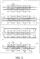
- Fig. 2 is a diagram showing an equivalent circuit of the light emitting device 1 according to Embodiment 1 of the present invention.
- the LED elements 3 to 6 are connected to each other in series using the wirings 71 to 75. Therefore, as shown in Fig. 2 , an equivalent circuit in which the LED elements 3 to 6 are connected to each other in series is formed in the light emitting device 1. Once the LED elements 3 to 6 are driven using the external drive circuit, the LED elements 3 to 6 emit light at the same time.
- the light emitting device 1 is suitably utilized as a light emitting device in which the LED elements 3 and 6 are arranged on a straight line, which can be incorporated in an edge light type backlight device.
- the light emitting device 1 illustrated in Fig. 1 does not have a printed board which is necessary for a light emitting device according to the related art and does not need a solder material for connecting a wiring and electrodes (positive electrode and negative electrodes). Thus, the following effects which contribute to miniaturizing and thinning of the light emitting device 1 can be obtained.
- the light emitting device 1 may be constituted of a light emitting element other than the LED elements 3 to 6, for example, an organic electro luminescence (EL) element or the like.
- EL organic electro luminescence
- Embodiment 2 of the present invention will be described below with reference to Figs. 3 to 5 .
- members having functions that are the same as those of the members described in the above-described embodiment will be denoted with the same reference numerals and description thereof will be omitted.
- Fig. 3 is a diagram showing a configuration of a light emitting device 1a according to Embodiment 2 of the present invention.
- (a) of Fig. 3 is a diagram of the light emitting device 1a viewed from a light emitting surface (front surface) thereof
- (b) of Fig. 3 is a diagram of the light emitting device 1a viewed from a surface which is perpendicular to the light emitting surface thereof (a lateral surface)
- (c) of Fig. 3 is a diagram of the light emitting device 1a viewed from a surface which is opposite to the light emitting surface thereof (a back surface).
- the light emitting device 1a includes a resin molded body 2, LED elements 3 to 6, and wirings 81 to 86.
- the LED element 3 includes a base part 31, a light emitting unit 32, a positive electrode 33a (another electrode), a positive electrode 33b (electrode), a negative electrode 34a (another electrode), and a negative electrode 34b (electrode).
- the LED element 4 includes a base part 41, a light emitting unit 42, a positive electrode 43a (another electrode), a positive electrode 44b (electrode), a negative electrode 44a (another electrode), and a negative electrode 44b (electrode).
- the LED element 5 includes a base part 51, a light emitting unit 52, a positive electrode 53a (another electrode), a positive electrode 53b (electrode), a negative electrode 54a (another electrode), and a negative electrode 54b (electrode).
- the LED element 6 includes a base part 61, a light emitting unit 62, a positive electrode 63a (another electrode), a positive electrode 63b (electrode), a negative electrode 64a (another electrode), and a negative electrode 64b (electrode).
- the positive electrode 33a and the negative electrode 34a are formed in the front surface (a surface which is perpendicular to a surface in which the light emitting unit 32 is formed) in the base part 31.
- the positive electrode 33b and the negative electrode 34b are formed in the back surface (a surface which is perpendicular to the surface in which the light emitting unit 32 is formed) which is opposite to the front surface in the base part 31.
- the positive electrodes 33a and 33b are integrally formed in an LED element 103. In other words, the positive electrodes 33a and 33b are electrically connected to each other.
- the negative electrodes 34a and 34b are integrally formed in the LED element 103. In other words, the negative electrodes 34a and 34b are electrically connected to each other.
- the positive electrodes 33a to 63a and the negative electrodes 34a to 64a are exposed on a front surface 21 (third surface) which is perpendicular to the lateral surface 22 (first surface) of the resin molded body 2.
- the positive electrodes 33b to 63b and the negative electrodes 34b to 64b are exposed on the back surface 23 (second surface) which is perpendicular to the lateral surface 22 of the resin molded body 2 and is opposite to the front surface 21.
- the wirings 81 to 86 are formed in the front surface 21 or the back surface 23 of the resin molded body 2 and are connected to at least any of the corresponding positive electrodes 33a to 63a, positive electrodes 33b to 63b, negative electrodes 34a to 64a, or negative electrodes 34b to 64b.
- the wirings 81 to 85 are formed on the front surface 21 or the back surface 23 of the resin molded body 2 using printing through, for example, a printing method using silver ink or the like. Therefore, a solder material is not required for a connection between the wirings 81 to 85 and the positive electrodes 33a to 63a, the positive electrodes 33b to 63b, the negative electrodes 34a to 64a, or the negative electrodes 34b to 64b.
- one end of the wiring 81 is connected to the positive electrode 33b.
- the other end of the wiring 81 is connected to a drive circuit (not shown) outside of the light emitting device 1a.
- One end of the wiring (another wiring) 82 is connected to the positive electrode 33a and the other end thereof is connected to the positive electrode 43a. In this way, the wiring 82 serves to connect the positive electrode 33a of the LED element 3 and the positive electrode 43a of the LED element 4.
- One end of the wiring 83 is connected to the negative electrode 34b and the other end thereof is connected to the positive electrode 53b.
- the wiring 73 serves to connect the LED element 3 and the LED element 5.
- One end of the wiring 84 (another wiring) is connected to the negative electrode 44a and the other end thereof is connected to the positive electrode 63a. In this way, the wiring 84 serves to connect the LED element 4 and the LED element 6.
- One end of the wiring 85 is connected to the negative electrode 54b and the other end thereof is connected to the negative electrode 64b. In this way, the wiring 85 serves to connect the negative electrode 54b of the LED element 5 and the negative electrode 64b of the LED element 6.
- One end of the wiring 86 is connected to the negative electrode 64b.
- the other end of the wiring 86 is connected to the drive circuit (not shown) outside of the light emitting device 1a.
- the light emitting device 1a groups of wirings are formed in the front surface 21 and the back surface 23 of the resin molded body 2.
- the positive electrode 33b of the LED element 103 commonly connects the wiring 82 of the front surface 21 and the wiring 83 of the back surface 23.
- the negative electrode 64b of an LED element 106 commonly connects the wiring 84 of the front surface 21 and the wiring 85 of the back surface 23.
- Fig. 4 is a diagram showing an equivalent circuit of the light emitting device 1a according to Embodiment 2 of the present invention.
- the LED elements 3 and 5 are connected to each other in series using the wirings 82 and 84.
- the LED elements 4 and 6 are connected to each other in series using the wirings 83 and 85.
- the LED elements 3 and 5 and the LED elements 4 and 6 are connected to each other in parallel. Therefore, as shown in Fig.
- the equivalent circuit in which the LED elements 3 and 5 are connected to each other in series, the LED elements 4 and 6 are connected to each other in series, and the LED elements 3 and 5 and the LED elements 4 and 6 are connected to each other in parallel is formed.
- the LED elements 3 to 6 When the LED elements 3 to 6 are driven using the external drive circuit, the LED elements 3 to 6 emit light at the same time. Furthermore, since there is no hindrance to electric power supply toward the LED elements 4 and 6 even when the LED elements 3 and 5 are turned off due to a disconnection occurring in the wiring 82 or 84 formed in the front surface 21 of the resin molded body 2, the LED elements 4 and 6 remain on. Conversely, since there is no hindrance to electric power supply to the LED elements 3 and 5 even when the LED elements 4 and 6 are turned off due to a disconnection occurring in the wiring 83 or 85 formed in the back surface 23 of the resin molded body 2, the LED elements 3 and 5 remain on.
- the light emitting device 1a is also suitably utilized as a light emitting device in which the LED elements 3 to 6 are arranged in a straight line, which can be incorporated in an edge light type backlight device.
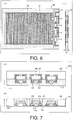
- Fig. 5 is a diagram for describing a method for manufacturing the light emitting device 1a according to the embodiment. The manufacturing method of the light emitting device 1a according to the embodiment will be described below with reference to the drawing.
- temporary fixing films 11 and 12 for temporarily fixing the LED elements 3 to 6 were prepared and the LED elements 3 to 6 were temporarily fixed to the temporary fixing films 11 and 12.
- the temporary fixing films 11 and 12 include films made of polyethylene terephthalate (PET).
- the LED elements 3 to 6 were temporarily fixed to the temporary fixing films 11 and 12 using an adhesive or the like so that the positive electrodes 33a to 63a and the negative electrodes 34a to 64a of the LED elements 3 to 6 were in contact with the temporary fixing film 11 and the positive electrodes 33b to 63b and the negative electrodes 34b to 64b of the LED elements 3 to 6 were in contact with the temporary fixing film 12.
- an ultraviolet curable adhesive (not shown) applied to the temporary fixing films 11 and 12 could be used.
- an adhesive was applied to the temporary fixing film 11 made of PET of 50 ⁇ m to have a thickness of 2 to 3 ⁇ m using GL-3005H manufactured by Gluelabo Ltd. as an adhesive.
- the temporary fixing films 11 and 12 in which the LED elements 3 to 6 prepared in a temporary fixing process were temporarily fixed were arranged in a gap between a mold 13 and a mold 14 and then a resin material was injected into the gap.
- injection molding of a resin material was performed so that the LED elements 3 to 6 were embedded in the resin molded body 2.
- Examples of a resin material used in such a process include various resin materials such as PC and ABS.
- PC When PC was used, PC was used at an injection temperature of 270 °C and an injection pressure of 100 Mpa.
- ABS ABS was used at an injection temperature of 180 °C and an injection pressure 20 kgf/cm 2 .
- a PET film used as the temporary fixing film 11 was greatly deformed due to heat during the injection molding in the injection molding process and was peeled off the injection molding product. For this reason, the temporary fixing film 11 can be easily peeled off the injection molding product.
- the wirings 82 and 84 connected to the positive electrodes 33a to 63a and the negative electrodes 34a to 64a of the LED elements 3 to 6 exposed on the front surface 21 of the resin molded body 2 are formed in the front surface 21 of the resin molded body 2.
- the wirings 81, 83, 85, and 86 connected to the positive electrodes 33b to 63b and the negative electrodes 34b to 64b of the LED elements 3 to 6 exposed on the back surface 23 of the resin molded body 2 were formed in the back surface 23 of the resin molded body 2.
- the light emitting device 1 was completed.
- Various methods can be used for forming the wirings 81 to 86. Examples of such methods include a method for printing the wirings 81 to 86 by injecting a conductive material (for example, silver ink or the like) using an inkjet printer or the like, a method for forming the wirings 81 to 86 using an aerosol, a method for forming the wirings 81 to 86 using a dispenser, or the like.
- a conductive material for example, silver ink or the like
- aerosol a method for forming the wirings 81 to 86 using a dispenser, or the like.
- a thickness of the manufactured light emitting device 1a can be formed to have a minimum thinness equal to a height (a thickness in an H direction) of the LED element 103. Furthermore, since a mounting distance (distance a illustrated in Fig. 6 ) between the LED elements 3 to 6 may be about 0.2 to 0.3 mm serving as a minimum distance in which the resin material flows during the injection molding process, arrangement of the LED elements 3 to 6 having narrow pitches in which the arrangement is impossible in the related art can be realized.
- the LED elements 3 to 6 are embedded in the resin molded body 2 to be fixed in the resin molded body 2, mounting positions of the LED elements 3 to 6 in the light emitting device 1a are accurately determined in accordance with installation positions of the LED elements 3 to 6 in the temporary fixing films 11 and 12 in the temporary fixing process.
- the following effects can be obtained.
- the light emitting device 1 according to Embodiment 1 illustrated in Fig. 1 can be manufactured by a method that is basically the same as the manufacturing method illustrated in Fig. 5 .
- the LED elements 3 to 6 may be temporarily fixed only to the temporary fixing film 12 during the temporary fixing process, and thus the temporary fixing film 11 need not be used.
- the wiring since the wiring may be formed only in the back surface 23 of the resin molded body 2 during the wiring forming process, the wiring forming process in the front surface 21 of the resin molded body 2 illustrated in (d) of Fig. 5 is also unnecessary.
- Embodiment 3 of the present invention will be described below with reference to Fig. 6 .
- members having functions that are the same as that of the members described in the above-described embodiment will be denoted with the same reference numerals and description thereof will be omitted.
- Fig. 6 is a diagram showing a configuration of a backlight device 90 according to Embodiment 3 of the present invention.
- (a) of Fig. 6 is a diagram of the backlight device 90 viewed from an upper surface thereof
- (b) of Fig. 6 is a diagram of the light emitting device 1a mounted in the backlight device 90 viewed from a light emitting surface thereof.
- the backlight device 90 includes a resin frame 91, a light guide plate 92, and a light emitting device 1a.
- the resin frame 91 fixes the light guide plate 92 to be arranged to surround the light guide plate 92.
- the light emitting device 1a is arranged in such a way that the light emitting surface thereof faces any lateral surface in the light guide plate 92. Furthermore, the light emitting device 1a is embedded in the resin frame 91.
- the backlight device 90 can be suitably used for various display devices as an edge light type backlight device.
- An edge light type backlight device is widely used in various display devices such as a display module of a portable type terminal device, a laptop type personal computer, and a liquid crystal monitor. At present, thinning of the edge light type backlight device is strongly required along with thinning of such devices.
- a thickness of the light emitting device 1a according to the embodiment can be substantially the same as a thickness of the LED elements 3 to 6, an LED mounting part of the backlight device 90 including the light emitting device 1a can be minimized to the thickness of the LED elements 3 to 6. Therefore, the backlight device 90 can be made thinner.
- the light emitting device 1a is embedded in the resin frame 91 in the backlight device 90, a size of the backlight device 90 in a plane direction can also be decreased.
- a light emitting device includes: a resin molded body; a light emitting element including at least a light emitting unit and an electrode and embedded in the resin molded body so that the light emitting unit is exposed on a first surface in the resin molded body and the electrode is exposed on a second surface which is perpendicular to the first surface in the resin molded body; and a wiring formed in the second surface in the resin molded body and connected to the electrode.
- the light emitting element is mounted in the light emitting device in such a way that the light emitting element is embedded in the resin molded body. For this reason, since a printed board configured to mount the light emitting element is not required, a height of the light emitting device can be made to substantially match a height of the light emitting element (resin molded body). Furthermore, since a wiring connected to the electrode of the light emitting element exposed on the second surface of the resin molded body can be formed using printing, a solder material for connection need not be used. Thus, since a space for a solder material between light emitting elements becomes unnecessary, mounting pitches between the light emitting elements can be minimized.
- the light emitting device which is further miniaturized and thinned can be realized.
- a plurality of light emitting elements are embedded in the resin molded body and the electrodes included in the light emitting elements are connected to each other through the wirings.
- the light emitting device including the plurality of light emitting elements can be realized.
- a plurality of light emitting elements are embedded in the resin molded body, each of the light emitting elements include another electrode, the other electrode is exposed on a third surface which is perpendicular to the first surface of the resin molded body and faces the second surface thereof, and another wiring formed in the third surface of the resin molded body and connected to the other electrode is further provided.
- the light emitting device including the plurality of light emitting elements can be realized.
- the electrode and the other electrode are integrally formed.
- a wiring in a second surface of a resin molded body and a wiring in a third surface of the resin molded body can be electrically connected to each other through an electrode or another electrode.
- the plurality of light emitting elements are linearly arranged.
- the light emitting device which can be suitably incorporated in an edge light type backlight device can be realized.
- the light emitting element is a light emitting diode (LED) element.
- the light emitting device with low power consumption can be realized.
- a backlight device includes: a light guide plate; and any of the above-described light emitting devices arranged to face any lateral surface of the light guide plate.
- the backlight device which is further miniaturized and thinned can be realized.
- a backlight device further includes: a resin frame to which the light guide plate is fixed, wherein the light emitting device is embedded in the resin frame.
- a size of the backlight device in a plane direction can be decreased.
- a manufacturing method of a light emitting device includes: a step of temporarily fixing a light emitting element including at least a light emitting unit and an electrode formed in a surface which is perpendicular to a surface in which the light emitting unit is formed to a temporary fixing film in such a way that the electrode is in contact with the temporary fixing film; a step of forming a resin molded body in which the light emitting element is embedded by arranging the temporary fixing film in which the light emitting element is temporarily fixed in a gap in a mold and injecting a resin material into the gap; a step of peeling the temporary fixing film off the resin molded body; and a step of forming a wiring connected to the electrode in a surface on which the electrode in the resin molded body is exposed.
- the light emitting device which is further miniaturized and thinned can be more easily manufactured.
Landscapes
- Physics & Mathematics (AREA)
- General Physics & Mathematics (AREA)
- Optics & Photonics (AREA)
- Engineering & Computer Science (AREA)
- Microelectronics & Electronic Packaging (AREA)
- Led Device Packages (AREA)
- Planar Illumination Modules (AREA)
- Electroluminescent Light Sources (AREA)
Abstract
Description
- The present invention relates to a light emitting device including light emitting elements such as light emitting diode (LED) elements.
- In the related art, a backlight including a plurality of light emitting diode (LED) elements is generally used as an electronic component configured to illuminate a liquid crystal display from a back surface thereof. Furthermore, there are edge light type and direct type systems as such a backlight, and an edge light type is used for a small liquid crystal used for a portable terminal or the like, a laptop type personal computer, a liquid crystal monitor, and the like.
- In an edge light type backlight, a plurality of LED elements are arranged in any lateral surface of a plate-like light guide plate and the entire surface of a liquid crystal panel is irradiated with light through the light guide plate. Since the number of required LED elements is smaller in such a type than that of a direct type, the edge light type backlight has advantages such as low cost, energy saving, and a liquid crystal display which can be made thin.
- In recent years, an edge light type backlight is required to be thinner than in the related art, and molding processing used to make a plate-like light guide plate to 0.3 mm or less or an LED element with a thickness of 0.3 mm is being developed.
- In the related art, in order to arrange a plurality of LED elements for a backlight, a method for soldering the LED elements in a printed board using a solder material is mainly performed. However, such a method has a limitation on further thinning of the backlight.
-
Fig. 7 is a diagram showing a configuration of alight emitting device 101 according to the related art. As shown in (a) ofFig. 7 , thelight emitting device 101 includes a printedboard 102 and a plurality ofLED elements 103. Furthermore, as shown in (a) and (b) ofFig. 7 , each of theLED elements 103 includes abase part 131, alight emitting unit 132, apositive electrode 133, and anegative electrode 134. - A
wiring 121 is formed in a front surface of the printedboard 102 using a method such as etching. Furthermore, the printedboard 102 is assembled with aresin casing 105. - The
light emitting unit 132 constituted of a light emitting diode is provided in a first surface of thebase part 131. In addition, thepositive electrode 133 and thenegative electrode 134 are provided in a second surface which is perpendicular to the first surface of thebase part 131. In each ofLED elements 103, thepositive electrode 133 and thenegative electrode 134 are connected to thewiring 121 using asolder material 122 to be mounted in the front surface of the printedboard 102. - However, like in the
light emitting device 101 illustrated inFig. 7 , since a thickness of a printedboard 101, a thickness of thewiring 121, a floating thickness of a joint using thesolder material 122, and a thickness of a space required for assembly of the printedboard 102 and theresin casing 105 are required in a configuration in which theLED elements 103 are mounted in the front surface of the printedboard 102, there is a problem in that a height (thickness in an H direction) of thelight emitting device 101 is obtained by adding a thickness of at least about 0.1 mm to a thickness of theLED element 103. - As a countermeasure against such a problem, the
light emitting device 101a of a configuration illustrated inFig. 8 can be considered. -
Fig. 8 is a diagram showing a configuration of alight emitting device 101a according to the related art. In thelight emitting device 101a illustrated in the drawing, thepositive electrode 133 and thenegative electrode 134 are provided in an opposite side to thelight emitting unit 132 of theLED element 103 and connected to thewiring 121 in the printedboard 102 via asolder material 104. Since a height (thickness in an H direction) of the printedboard 102 is substantially the same as a height of theLED element 103 in such a configuration, a thickness of thelight emitting device 101a can be made as thin as a thickness of theLED element 103. - However, in order to realize the
light emitting device 101a with such a configuration, it is necessary to prepare the printedboard 102 with a narrow width such as 0.3 mm. Since processing of obtaining such a printedboard 102 is very difficult, there is a problem regarding an increase in manufacturing costs of thelight emitting device 101a. In addition, since a connection area between theLED element 103 and the printedboard 102 is decreased, there is also concern that a mounting strength of theLED element 103 will be insufficient. - In addition, miniaturization of a light emitting device is required due to an increasing demand for miniaturization and thinning of electronic devices in recent years. However, in the light emitting device 101 (101a) obtained through a mounting method using the
solder material 122 in the related art, it is necessary to secure an installation space of thesolder material 122 in the light emitting device 101 (101a) in view of wet spreading of thesolder material 122, securing a mounting strength, or the like. Therefore, there is a limit to miniaturization of the light emitting device 101 (101a). - Thus, in the related art, various proposals have been provided as countermeasures to deal with positional deviation of an LED at the time of surface mounting using a solder material.
- Patent Literature 1 discloses a method for fixing an LED mounting position by forming a groove in the LED mounting position in a printed board and inserting an LED member joined to a dummy having a dimension which is the same as a mounting pitch of an LED into the groove.
-
Patent Literature 2 discloses a method for fixing an LED mounting position by putting an adhesive into a hole formed in a printed board, mounting an LED above the adhesive, and curing the adhesive. -
Patent Literature 3 discloses a method for fixing an LED mounting position by assembling an LED and a positioned member and then soldering the LED to a circuit of a printed board. -
- Patent Literature 1: Japanese Patent Application Laid-Open (
JP-A) No. S64-25582 (published on January 27, 1989 - Patent Literature 2: Japanese Patent Application Laid-Open (
JP-A) No. H11-219961 (published on August 10, 1999 - Patent Literature 3: Japanese Patent Application Laid-Open (
JP-A) No. 2008-16297 (published on January 24, 2008 - Patent Literature 4: Japanese Patent Application Laid-Open (
JP-A) No. H5-150807 (published on July 30, 1993 - Patent Literature 5: Japanese Patent Application Laid-Open (
JP-A) No. H9-179512 (published on July 11, 1997 - However, in the related art, it is difficult to realize accuracy of an LED mounting position in units of microns in view of processing accuracy of a board, processing accuracy of a dummy member, an assembly member, and the like. In addition, since a processing space for a groove or a hole or an installation space for a dummy member or an assembly member is required, there is a problem regarding an increase in size of a light emitting device. There is also a problem regarding a decrease in manufacturing yield due to complicated manufacturing processes such as additional processing of a printed board or an increase in manufacturing costs due to preparation of an assembly member.
- The present invention was made to solve the above-described problems. Moreover, an object of the present invention is to realize a light emitting device which is further miniaturized and thinned, a backlight device including such a light emitting device, and a manufacturing method for more easily manufacturing such a light emitting device.
- In order to solve the above-described problems, a light emitting device according to an aspect of the present invention includes: a resin molded body; a light emitting element including at least a light emitting unit and an electrode and embedded in the resin molded body so that the light emitting unit is exposed on a first surface in the resin molded body and the electrode is exposed on a second surface which is perpendicular to the first surface in the resin molded body; and a wiring formed in the second surface in the resin molded body and connected to the electrode.
- In order to solve the above-described problems, a backlight device according to an aspect of the present invention includes: a light guide plate; and the light emitting devices described above arranged to face any lateral surface of the light guide plate.
- In order to solve the above-described problems, a manufacturing method of a light emitting device according to an aspect of the present invention includes: a step of temporarily fixing a light emitting element including at least a light emitting unit and an electrode formed in a surface which is perpendicular to a surface in which the light emitting unit is formed to a temporary fixing film in such a way that the electrode is in contact with the temporary fixing film; a step of forming a resin molded body in which the light emitting element is embedded by arranging the temporary fixing film in which the light emitting element is temporarily fixed in a gap in a mold and injecting a resin material into the gap; a step of peeling the temporary fixing film off the resin molded body; and a step of forming a wiring connected to the electrode in a surface on which the electrode in the resin molded body is exposed.
- According to the present invention, a more compact and thinner light emitting device, a backlight device including such a light emitting device, and a manufacturing method for more easily manufacturing such a light emitting device can be realized.
-
-
Fig. 1 is a diagram showing a configuration of a light emitting device according to Embodiment 1 of the present invention. -
Fig. 2 is a diagram showing an equivalent circuit of the light emitting device according to Embodiment 1 of the present invention. -
Fig. 3 is a diagram showing a configuration of a light emitting device according toEmbodiment 2 of the present invention. -
Fig. 4 is a diagram showing an equivalent circuit of the light emitting device according toEmbodiment 2 of the present invention. -
Fig. 5 is a diagram for describing a method for manufacturing the light emitting device according toEmbodiment 2 of the present invention. -
Fig. 6 is a diagram showing a configuration of a backlight device according toEmbodiment 3 of the present invention. -
Fig. 7 is a diagram showing a configuration of a light emitting device in the related art. -
Fig. 8 is a diagram showing a configuration of a light emitting device in the related art. - Embodiment 1 of the present invention will be described below with reference to
Figs. 1 and 2 . -
Fig. 1 is a diagram showing a configuration of a light emitting device 1 according to Embodiment 1 of the present invention. (a) ofFig. 1 is a diagram of the light emitting device 1 viewed from a light emitting surface (front surface) thereof, (b) ofFig. 1 is a diagram of the light emitting device 1 viewed from a surface which is perpendicular to the light emitting surface (a lateral surface), and (c) ofFig. 1 is a diagram of the light emitting device 1 viewed from a surface which is opposite to the light emitting surface (a back surface). - As shown in
Fig. 1 , the light emitting device 1 includes a resin moldedbody 2, light emitting diode (LED)elements 3 to 6, and wirings 71 to 75. - The resin molded
body 2 serves as a board of the light emitting device 1 and is constituted of various resin materials. Examples of such materials include polycarbonate (PC) or acrylonitrile butadiene styrene (ABS). - The
LED elements 3 to 6 are surface mount (SMD) type LED elements. As shown inFig. 1 , theLED element 3 includes abase part 31, alight emitting unit 32, a positive electrode (electrode) 33, and a negative electrode (electrode) 34. TheLED element 4 includes abase part 41, alight emitting unit 42, a positive electrode (electrode) 43, and a negative electrode (electrode) 44. TheLED element 5 includes abase part 51, alight emitting unit 52, a positive electrode (electrode) 53, and a negative electrode (electrode) 54. TheLED element 6 includes abase part 61, alight emitting unit 62, a positive electrode (electrode) 63, and a negative electrode (electrode) 64. - The
base part 31 is a main body of theLED element 3. Thelight emitting unit 32 constituted of an LED is formed in a lateral surface of thebase part 31. When theLED element 3 emits light, the light is emitted from thelight emitting unit 32. Thepositive electrode 33 and thenegative electrode 34 are connection electrodes connected to an external part of the light emitting device 1 or any of theLED elements 4 to 6 in the light emitting device 1. Thepositive electrode 33 and thenegative electrode 34 are formed in a back surface (a second surface) which is perpendicular to the lateral surface of thebase part 31. - Since a detailed configuration of the
LED elements 4 to 6 is the same as that of theLED element 3, detailed description thereof will be omitted. - The
LED elements 3 to 6 are embedded in the resin moldedbody 2. As shown inFig. 1 , in the light emitting device 1, a plurality of (four)LED elements 3 to 6 are linearly arranged. As shown in (b) ofFig. 1 , thelight emitting units 32 to 62 are exposed on alateral surface 22 of the resin moldedbody 2. Therefore, as indicated by an arrow in (a) ofFig. 1 , when the light emitting device 1 emits light, the light is emitted from thelateral surface 22 of the resin moldedbody 2. - As shown in (c) of
Fig. 1 , thepositive electrodes 33 to 63 and thenegative electrodes 34 to 64 are exposed on aback surface 23 which is perpendicular to thelateral surface 22 of the resin moldedbody 2. -
Wirings 71 to 75 are formed on theback surface 23 of the resin moldedbody 2 and are connected to at least any of the correspondingpositive electrodes 33 to 63 ornegative electrodes 34 to 64. Thewirings 71 to 75 are formed on theback surface 23 of the resin moldedbody 2 using printing through, for example, a printing method using silver ink or the like. Therefore, a solder material is not required for a connection between thewirings 71 to 75 and thepositive electrodes 33 to 63 or thenegative electrodes 34 to 64. - As shown in
Fig. 1 , one end of thewiring 71 is connected to thepositive electrode 33. The other end of thewiring 71 is connected to a drive circuit (not shown) outside of the light emitting device 1. One end of thewiring 72 is connected to thenegative electrode 34 and the other end thereof is connected to thepositive electrode 43. In this way, thewiring 72 serves to connect theLED element 3 and theLED element 4. - One end of the
wiring 73 is connected to thenegative electrode 44 and the other end thereof is connected to thepositive electrode 53. In this way, thewiring 73 serves to connect theLED element 4 and theLED element 5. - One end of the
wiring 74 is connected to thenegative electrode 54 and the other end thereof is connected to thepositive electrode 63. In this way, thewiring 74 serves to connect theLED element 5 and theLED element 6. - One end of the
wiring 75 is connected to thenegative electrode 64. The other end of thewiring 75 is connected to the drive circuit (not shown) outside of the light emitting device 1. -
Fig. 2 is a diagram showing an equivalent circuit of the light emitting device 1 according to Embodiment 1 of the present invention. As shown inFig. 1 , theLED elements 3 to 6 are connected to each other in series using thewirings 71 to 75. Therefore, as shown inFig. 2 , an equivalent circuit in which theLED elements 3 to 6 are connected to each other in series is formed in the light emitting device 1. Once theLED elements 3 to 6 are driven using the external drive circuit, theLED elements 3 to 6 emit light at the same time. - The light emitting device 1 according to the embodiment is suitably utilized as a light emitting device in which the
LED elements - The light emitting device 1 illustrated in
Fig. 1 does not have a printed board which is necessary for a light emitting device according to the related art and does not need a solder material for connecting a wiring and electrodes (positive electrode and negative electrodes). Thus, the following effects which contribute to miniaturizing and thinning of the light emitting device 1 can be obtained. - (1) Since a height of the light emitting device 1 can be reduced to a minimum value that is substantially the same as a height of the
LED elements 3 to 6, the light emitting device 1 can be thinned. - (2) Since spaces among the
LED elements 3 to 6 necessary for connection between electrodes and wirings of the LED elements using a solder material in the related art are not required for the light emitting device 1, pitches (intervals among theLED elements 3 to 6) when theLED elements 3 to 6 are mounted in the light emitting device 1 can be made smaller than those of the related art. - (3) Since the
LED elements 3 to 6 are embedded in the resin moldedbody 2, a mounting strength of anLED element 103 is higher than a connection structure using a solder material like in the related art. - The light emitting device 1 may be constituted of a light emitting element other than the
LED elements 3 to 6, for example, an organic electro luminescence (EL) element or the like. -
Embodiment 2 of the present invention will be described below with reference toFigs. 3 to 5 . Note that, for convenience of explanation, members having functions that are the same as those of the members described in the above-described embodiment will be denoted with the same reference numerals and description thereof will be omitted. -
Fig. 3 is a diagram showing a configuration of alight emitting device 1a according toEmbodiment 2 of the present invention. (a) ofFig. 3 is a diagram of thelight emitting device 1a viewed from a light emitting surface (front surface) thereof, (b) ofFig. 3 is a diagram of thelight emitting device 1a viewed from a surface which is perpendicular to the light emitting surface thereof (a lateral surface), and (c) ofFig. 3 is a diagram of thelight emitting device 1a viewed from a surface which is opposite to the light emitting surface thereof (a back surface). - As shown in
Fig. 3 , thelight emitting device 1a includes a resin moldedbody 2,LED elements 3 to 6, and wirings 81 to 86. TheLED element 3 includes abase part 31, alight emitting unit 32, apositive electrode 33a (another electrode), apositive electrode 33b (electrode), anegative electrode 34a (another electrode), and anegative electrode 34b (electrode). TheLED element 4 includes abase part 41, alight emitting unit 42, apositive electrode 43a (another electrode), apositive electrode 44b (electrode), anegative electrode 44a (another electrode), and anegative electrode 44b (electrode). TheLED element 5 includes abase part 51, alight emitting unit 52, apositive electrode 53a (another electrode), apositive electrode 53b (electrode), anegative electrode 54a (another electrode), and anegative electrode 54b (electrode). TheLED element 6 includes abase part 61, alight emitting unit 62, apositive electrode 63a (another electrode), apositive electrode 63b (electrode), anegative electrode 64a (another electrode), and anegative electrode 64b (electrode). - In the
LED element 3, thepositive electrode 33a and thenegative electrode 34a are formed in the front surface (a surface which is perpendicular to a surface in which thelight emitting unit 32 is formed) in thebase part 31. On the other hand, thepositive electrode 33b and thenegative electrode 34b are formed in the back surface (a surface which is perpendicular to the surface in which thelight emitting unit 32 is formed) which is opposite to the front surface in thebase part 31. Thepositive electrodes LED element 103. In other words, thepositive electrodes negative electrodes LED element 103. In other words, thenegative electrodes - Since a detailed configuration of the
LED elements 4 to 6 is the same as that of theLED element 3, detailed description thereof will be omitted. - As shown in (a) of
Fig. 3 , thepositive electrodes 33a to 63a and thenegative electrodes 34a to 64a are exposed on a front surface 21 (third surface) which is perpendicular to the lateral surface 22 (first surface) of the resin moldedbody 2. On the other hand, as shown in (b) ofFig. 3 , thepositive electrodes 33b to 63b and thenegative electrodes 34b to 64b are exposed on the back surface 23 (second surface) which is perpendicular to thelateral surface 22 of the resin moldedbody 2 and is opposite to thefront surface 21. - The
wirings 81 to 86 are formed in thefront surface 21 or theback surface 23 of the resin moldedbody 2 and are connected to at least any of the correspondingpositive electrodes 33a to 63a,positive electrodes 33b to 63b,negative electrodes 34a to 64a, ornegative electrodes 34b to 64b. Thewirings 81 to 85 are formed on thefront surface 21 or theback surface 23 of the resin moldedbody 2 using printing through, for example, a printing method using silver ink or the like. Therefore, a solder material is not required for a connection between thewirings 81 to 85 and thepositive electrodes 33a to 63a, thepositive electrodes 33b to 63b, thenegative electrodes 34a to 64a, or thenegative electrodes 34b to 64b. - As shown in (c) of
Fig. 3 , one end of thewiring 81 is connected to thepositive electrode 33b. The other end of thewiring 81 is connected to a drive circuit (not shown) outside of thelight emitting device 1a. One end of the wiring (another wiring) 82 is connected to thepositive electrode 33a and the other end thereof is connected to thepositive electrode 43a. In this way, thewiring 82 serves to connect thepositive electrode 33a of theLED element 3 and thepositive electrode 43a of theLED element 4. - One end of the
wiring 83 is connected to thenegative electrode 34b and the other end thereof is connected to thepositive electrode 53b. In this way, thewiring 73 serves to connect theLED element 3 and theLED element 5. - One end of the wiring 84 (another wiring) is connected to the
negative electrode 44a and the other end thereof is connected to thepositive electrode 63a. In this way, thewiring 84 serves to connect theLED element 4 and theLED element 6. - One end of the
wiring 85 is connected to thenegative electrode 54b and the other end thereof is connected to thenegative electrode 64b. In this way, thewiring 85 serves to connect thenegative electrode 54b of theLED element 5 and thenegative electrode 64b of theLED element 6. - One end of the
wiring 86 is connected to thenegative electrode 64b. The other end of thewiring 86 is connected to the drive circuit (not shown) outside of thelight emitting device 1a. - As described above, in the
light emitting device 1a, groups of wirings are formed in thefront surface 21 and theback surface 23 of the resin moldedbody 2. Thepositive electrode 33b of theLED element 103 commonly connects thewiring 82 of thefront surface 21 and thewiring 83 of theback surface 23. Thenegative electrode 64b of an LED element 106 commonly connects thewiring 84 of thefront surface 21 and thewiring 85 of theback surface 23. With such a configuration, an equivalent circuit illustrated inFig. 4 is formed in thelight emitting device 1a. -
Fig. 4 is a diagram showing an equivalent circuit of thelight emitting device 1a according toEmbodiment 2 of the present invention. As shown inFig. 3 , in thelight emitting device 1a, theLED elements wirings LED elements wirings LED elements LED elements Fig. 2 , in thelight emitting device 1a, the equivalent circuit in which theLED elements LED elements LED elements LED elements - When the
LED elements 3 to 6 are driven using the external drive circuit, theLED elements 3 to 6 emit light at the same time. Furthermore, since there is no hindrance to electric power supply toward theLED elements LED elements wiring front surface 21 of the resin moldedbody 2, theLED elements LED elements LED elements wiring back surface 23 of the resin moldedbody 2, theLED elements LED elements 3 to 6 are turned off and half thereof remain on even when a disconnection has occurred in any of thewirings 82 to 84 in thelight emitting device 1a, a certain degree of illuminance can be maintained even when a disconnection occurs. - The
light emitting device 1a according to the embodiment is also suitably utilized as a light emitting device in which theLED elements 3 to 6 are arranged in a straight line, which can be incorporated in an edge light type backlight device. -
Fig. 5 is a diagram for describing a method for manufacturing thelight emitting device 1a according to the embodiment. The manufacturing method of thelight emitting device 1a according to the embodiment will be described below with reference to the drawing. - First, as shown in (a) of
Fig. 5 ,temporary fixing films LED elements 3 to 6 were prepared and theLED elements 3 to 6 were temporarily fixed to thetemporary fixing films temporary fixing films - In the embodiment, the
LED elements 3 to 6 were temporarily fixed to thetemporary fixing films positive electrodes 33a to 63a and thenegative electrodes 34a to 64a of theLED elements 3 to 6 were in contact with thetemporary fixing film 11 and thepositive electrodes 33b to 63b and thenegative electrodes 34b to 64b of theLED elements 3 to 6 were in contact with thetemporary fixing film 12. For such temporary fixing, for example, an ultraviolet curable adhesive (not shown) applied to thetemporary fixing films temporary fixing film 11 made of PET of 50 µm to have a thickness of 2 to 3 µm using GL-3005H manufactured by Gluelabo Ltd. as an adhesive. - Subsequently, positions of the
LED elements 3 to 6 in thetemporary fixing films LED elements 3 to 6 were installed in the positions determined in thetemporary fixing films temporary fixing films LED elements 3 to 6 with ultraviolet rays of 3000 mJ/cm2. Thus, theLED elements 3 to 6 were temporarily fixed to thetemporary fixing films - Subsequently, as shown in (b) of
Fig. 5 , thetemporary fixing films LED elements 3 to 6 prepared in a temporary fixing process were temporarily fixed were arranged in a gap between amold 13 and amold 14 and then a resin material was injected into the gap. Thus, injection molding of a resin material was performed so that theLED elements 3 to 6 were embedded in the resin moldedbody 2. - Examples of a resin material used in such a process include various resin materials such as PC and ABS. When PC was used, PC was used at an injection temperature of 270 °C and an injection pressure of 100 Mpa. When ABS was used, ABS was used at an injection temperature of 180 °C and an injection pressure 20 kgf/cm2.
- Subsequently, as shown in (c) of
Fig. 5 , an injection molding product obtained in the injection molding process was taken out from the gap between themold 13 and themold 14 and then thetemporary fixing films light emitting units 32 to 62 of theLED elements 3 to 6 were exposed on thelateral surface 22 of the resin moldedbody 2. On the other hand, thepositive electrodes 33a to 63a and thenegative electrodes 34 to 64 of theLED elements 3 to 6 were exposed on thefront surface 21 of the resin moldedbody 2 and thepositive electrodes 33b to 63b and thenegative electrodes 34b to 64b of theLED elements 3 to 6 were exposed on theback surface 23 of the resin moldedbody 2. - Note that a PET film used as the
temporary fixing film 11 was greatly deformed due to heat during the injection molding in the injection molding process and was peeled off the injection molding product. For this reason, thetemporary fixing film 11 can be easily peeled off the injection molding product. - Finally, as shown in (d) of
Fig. 5 , thewirings positive electrodes 33a to 63a and thenegative electrodes 34a to 64a of theLED elements 3 to 6 exposed on thefront surface 21 of the resin moldedbody 2 are formed in thefront surface 21 of the resin moldedbody 2. In addition, thewirings positive electrodes 33b to 63b and thenegative electrodes 34b to 64b of theLED elements 3 to 6 exposed on theback surface 23 of the resin moldedbody 2 were formed in theback surface 23 of the resin moldedbody 2. Thus, the light emitting device 1 was completed. - Various methods can be used for forming the
wirings 81 to 86. Examples of such methods include a method for printing thewirings 81 to 86 by injecting a conductive material (for example, silver ink or the like) using an inkjet printer or the like, a method for forming thewirings 81 to 86 using an aerosol, a method for forming thewirings 81 to 86 using a dispenser, or the like. - According to the manufacturing method of the embodiment, a thickness of the manufactured
light emitting device 1a can be formed to have a minimum thinness equal to a height (a thickness in an H direction) of theLED element 103. Furthermore, since a mounting distance (distance a illustrated inFig. 6 ) between theLED elements 3 to 6 may be about 0.2 to 0.3 mm serving as a minimum distance in which the resin material flows during the injection molding process, arrangement of theLED elements 3 to 6 having narrow pitches in which the arrangement is impossible in the related art can be realized. - In the manufacturing method of the
light emitting device 1a according to the embodiment, since theLED elements 3 to 6 are embedded in the resin moldedbody 2 to be fixed in the resin moldedbody 2, mounting positions of theLED elements 3 to 6 in thelight emitting device 1a are accurately determined in accordance with installation positions of theLED elements 3 to 6 in thetemporary fixing films - (4) Accurate accuracy of about accuracy±50 µm in an LED element mounting machine is obtained as accuracy of mounting positions in a plane direction (X-Y direction) of the
LED elements 3 to 6 in thelight emitting device 1a. - (5) In addition, accuracy of positions of the
LED elements 3 to 6 in a height direction (H direction) in thelight emitting device 1a can be minimized within several µm of about an application thickness variation of the adhesive used in the temporary fixing process.
Also, since heat treatment at 260 °C or more required for curing a solder material in the related art is not required in the manufacturing method of thelight emitting device 1a according to the embodiment, the following effects can be obtained. - (6) Since high heat is not applied to the
LED elements 3 to 6, a change in light emission characteristic in theLED elements 3 to 6 can be minimized.
Since the manufacturing method of thelight emitting device 1a according to the embodiment does not have a process of adding a printed board, a process of forming an extremely narrow wiring or a process of forming wirings on both surfaces in a printed board, and a complicated process such as assembly of other members and theLED elements 3 to 6, the following effects can be obtained. - (7) A factor of decreasing a manufacturing yield of the
light emitting device 1a can be eliminated or parts costs and manufacturing costs of thelight emitting device 1a can be reduced. - Note that the light emitting device 1 according to Embodiment 1 illustrated in
Fig. 1 can be manufactured by a method that is basically the same as the manufacturing method illustrated inFig. 5 . Note that, when the light emitting device 1 illustrated inFig. 1 is manufactured, theLED elements 3 to 6 may be temporarily fixed only to thetemporary fixing film 12 during the temporary fixing process, and thus thetemporary fixing film 11 need not be used. In addition, since the wiring may be formed only in theback surface 23 of the resin moldedbody 2 during the wiring forming process, the wiring forming process in thefront surface 21 of the resin moldedbody 2 illustrated in (d) ofFig. 5 is also unnecessary. -
Embodiment 3 of the present invention will be described below with reference toFig. 6 . Note that, for convenience of explanation, members having functions that are the same as that of the members described in the above-described embodiment will be denoted with the same reference numerals and description thereof will be omitted. -
Fig. 6 is a diagram showing a configuration of abacklight device 90 according toEmbodiment 3 of the present invention. (a) ofFig. 6 is a diagram of thebacklight device 90 viewed from an upper surface thereof and (b) ofFig. 6 is a diagram of thelight emitting device 1a mounted in thebacklight device 90 viewed from a light emitting surface thereof. - As shown in (a) of
Fig. 6 , thebacklight device 90 includes aresin frame 91, alight guide plate 92, and alight emitting device 1a. Theresin frame 91 fixes thelight guide plate 92 to be arranged to surround thelight guide plate 92. Thelight emitting device 1a is arranged in such a way that the light emitting surface thereof faces any lateral surface in thelight guide plate 92. Furthermore, thelight emitting device 1a is embedded in theresin frame 91. - In the
light emitting device 1a having such a configuration, light emitted from the light emitting surface of thelight emitting device 1a is introduced from the lateral surface of thelight guide plate 92 into thelight guide plate 92, reflected inside thelight guide plate 92, and radiated from an upper surface of thelight guide plate 92. Therefore, thebacklight device 90 can be suitably used for various display devices as an edge light type backlight device. - An edge light type backlight device is widely used in various display devices such as a display module of a portable type terminal device, a laptop type personal computer, and a liquid crystal monitor. At present, thinning of the edge light type backlight device is strongly required along with thinning of such devices. Here, as shown in (b) of
Fig. 6 , since a thickness of thelight emitting device 1a according to the embodiment can be substantially the same as a thickness of theLED elements 3 to 6, an LED mounting part of thebacklight device 90 including thelight emitting device 1a can be minimized to the thickness of theLED elements 3 to 6. Therefore, thebacklight device 90 can be made thinner. - Also, since the
light emitting device 1a is embedded in theresin frame 91 in thebacklight device 90, a size of thebacklight device 90 in a plane direction can also be decreased. - In order to solve the above-described problems, a light emitting device according to an aspect of the present invention includes: a resin molded body; a light emitting element including at least a light emitting unit and an electrode and embedded in the resin molded body so that the light emitting unit is exposed on a first surface in the resin molded body and the electrode is exposed on a second surface which is perpendicular to the first surface in the resin molded body; and a wiring formed in the second surface in the resin molded body and connected to the electrode.
- According to the above configuration, the light emitting element is mounted in the light emitting device in such a way that the light emitting element is embedded in the resin molded body. For this reason, since a printed board configured to mount the light emitting element is not required, a height of the light emitting device can be made to substantially match a height of the light emitting element (resin molded body). Furthermore, since a wiring connected to the electrode of the light emitting element exposed on the second surface of the resin molded body can be formed using printing, a solder material for connection need not be used. Thus, since a space for a solder material between light emitting elements becomes unnecessary, mounting pitches between the light emitting elements can be minimized.
- As described above, according to the above configuration, the light emitting device which is further miniaturized and thinned can be realized.
- In the light emitting device according to an aspect of the present invention, a plurality of light emitting elements are embedded in the resin molded body and the electrodes included in the light emitting elements are connected to each other through the wirings.
- According to the above configuration, the light emitting device including the plurality of light emitting elements can be realized.
- In the light emitting device according to an aspect of the present invention, a plurality of light emitting elements are embedded in the resin molded body, each of the light emitting elements include another electrode, the other electrode is exposed on a third surface which is perpendicular to the first surface of the resin molded body and faces the second surface thereof, and another wiring formed in the third surface of the resin molded body and connected to the other electrode is further provided.
- According to the above configuration, the light emitting device including the plurality of light emitting elements can be realized.
- In the light emitting device according to an aspect of the present invention, the electrode and the other electrode are integrally formed.
- According to the above configuration, a wiring in a second surface of a resin molded body and a wiring in a third surface of the resin molded body can be electrically connected to each other through an electrode or another electrode. Thus, the light emitting device with a configuration in which some of the plurality of light emitting elements of the plurality of light emitting elements and the others thereof are connected in parallel can be realized.
- In a light emitting device according to an aspect of the present invention, the plurality of light emitting elements are linearly arranged.
- According to the above configuration, the light emitting device which can be suitably incorporated in an edge light type backlight device can be realized.
- In a light emitting device according to an aspect of the present invention, the light emitting element is a light emitting diode (LED) element.
- According to the above configuration, the light emitting device with low power consumption can be realized.
- In order to solve the above-described problems, a backlight device according to an aspect of the present invention includes: a light guide plate; and any of the above-described light emitting devices arranged to face any lateral surface of the light guide plate.
- According to the above configuration, the backlight device which is further miniaturized and thinned can be realized.
- A backlight device according to an aspect of the present invention further includes: a resin frame to which the light guide plate is fixed, wherein the light emitting device is embedded in the resin frame.
- According to the above configuration, a size of the backlight device in a plane direction can be decreased.
- In order to solve the above-described problems, a manufacturing method of a light emitting device according to an aspect of the present invention includes: a step of temporarily fixing a light emitting element including at least a light emitting unit and an electrode formed in a surface which is perpendicular to a surface in which the light emitting unit is formed to a temporary fixing film in such a way that the electrode is in contact with the temporary fixing film; a step of forming a resin molded body in which the light emitting element is embedded by arranging the temporary fixing film in which the light emitting element is temporarily fixed in a gap in a mold and injecting a resin material into the gap; a step of peeling the temporary fixing film off the resin molded body; and a step of forming a wiring connected to the electrode in a surface on which the electrode in the resin molded body is exposed.
- According to the above configuration, the light emitting device which is further miniaturized and thinned can be more easily manufactured.
- The present invention is not limited to the above-described embodiments and various modifications thereof are possible within the scope of the claims. Embodiments obtained by appropriately combining technical means disclosed in different embodiments are also included in the technical scope of the present invention. New technical features can also be formed by combining technical means disclosed in embodiments.
-
- 1, 1a Light emitting device
- 2 Resin molded body
- 3 to 6 LED element (light emitting element)
- 11, 12 Temporary fixing film
- 13, 14 Mold
- 31 to 61 Base part
- 32 to 62 Light emitting unit
- 33 to 63 Positive electrode
- 33a to 63a Positive electrode (another electrode)
- 33b to 63b Positive electrode (electrode)
- 34 to 64 Negative electrode
- 34a to 64a Negative electrode (another electrode)
- 34b to 64b Negative electrode (electrode)
- 71 to 75 Wiring
- 81 to 86 Wiring (wiring, another wiring)
- 90 Backlight device
- 91 Resin frame
- 92 Light guide plate
Claims (9)
- A light emitting device comprising:a resin molded body;a light emitting element comprising at least a light emitting unit and an electrode, and embedded in the resin molded body so that the light emitting unit is exposed on a first surface in the resin molded body and the electrode is exposed on a second surface which is perpendicular to the first surface in the resin molded body; anda wiring formed in the second surface in the resin molded body and connected to the electrode.
- The light emitting device according to claim 1, wherein a plurality of the light emitting elements are embedded in the resin molded body and a plurality of the electrodes comprised in the light emitting elements are connected to each other through a plurality of the wirings.
- The light emitting device according to claim 1, wherein a plurality of the light emitting elements are embedded in the resin molded body, each of the light emitting elements comprises an other electrode, the other electrode is exposed on a third surface which is perpendicular to the first surface of the resin molded body and faces the second surface thereof, and an other wiring formed in the third surface of the resin molded body and connected to the other electrode is further provided.
- The light emitting device according to claim 3, wherein the electrode and the other electrode are integrally formed.
- The light emitting device according to any one of claims 2 to 4, wherein the plurality of light emitting elements are linearly arranged.
- The light emitting device according to any one of claims 1 to 5, wherein the light emitting element is a light emitting diode (LED) element.
- A backlight device comprising:a light guide plate; andthe light emitting devices according to any one of claims 1 to 6 arranged to face any lateral surface of the light guide plate.
- The backlight device according to claim 7, further comprising:a resin frame to which the light guide plate is fixed,wherein the light emitting device is embedded in the resin frame.
- A manufacturing method of a light emitting device comprising:a step of temporarily fixing a light emitting element comprising at least a light emitting unit and an electrode formed in a surface which is perpendicular to a surface in which the light emitting unit is formed to a temporary fixing film in such a way that the electrode is in contact with the temporary fixing film;a step of forming a resin molded body in which the light emitting element is embedded by arranging the temporary fixing film in which the light emitting element is temporarily fixed in a gap in a mold and injecting a resin material into the gap;a step of peeling the temporary fixing film off the resin molded body; anda step of forming a wiring connected to the electrode in a surface on which the electrode in the resin molded body is exposed.
Applications Claiming Priority (2)
| Application Number | Priority Date | Filing Date | Title |
|---|---|---|---|
| JP2016013708A JP6645213B2 (en) | 2016-01-27 | 2016-01-27 | Light emitting device and method of manufacturing light emitting device |
| PCT/JP2016/085015 WO2017130553A1 (en) | 2016-01-27 | 2016-11-25 | Light emitting device, backlight device, and manufacturing method of light emitting device |
Publications (3)
| Publication Number | Publication Date |
|---|---|
| EP3410500A1 true EP3410500A1 (en) | 2018-12-05 |
| EP3410500A4 EP3410500A4 (en) | 2019-08-14 |
| EP3410500B1 EP3410500B1 (en) | 2020-12-16 |
Family
ID=59398036
Family Applications (1)
| Application Number | Title | Priority Date | Filing Date |
|---|---|---|---|
| EP16888137.3A Not-in-force EP3410500B1 (en) | 2016-01-27 | 2016-11-25 | Light emitting device, backlight device, and manufacturing method of light emitting device |
Country Status (5)
| Country | Link |
|---|---|
| US (1) | US10607967B2 (en) |
| EP (1) | EP3410500B1 (en) |
| JP (1) | JP6645213B2 (en) |
| CN (1) | CN107960135B (en) |
| WO (1) | WO2017130553A1 (en) |
Families Citing this family (6)
| Publication number | Priority date | Publication date | Assignee | Title |
|---|---|---|---|---|
| JP7169052B2 (en) | 2017-07-11 | 2022-11-10 | 株式会社ダイセル | Fresnel lens and manufacturing method thereof |
| GB2568535B (en) | 2017-11-20 | 2020-12-02 | Svitzer As | Line handling system for coupling together lines on a tugboat |
| CN110320704A (en) * | 2018-03-29 | 2019-10-11 | 京东方科技集团股份有限公司 | Area source and display device |
| CN108828841B (en) * | 2018-07-26 | 2021-01-15 | 武汉华星光电技术有限公司 | LED backlight device and LED display device |
| CN110456570B (en) * | 2019-08-09 | 2021-11-16 | 佛山市国星光电股份有限公司 | LED backlight module and display device |
| TWI842468B (en) * | 2023-04-07 | 2024-05-11 | 晶呈科技股份有限公司 | Light-emitting diode package structure and manufacturing method thereof |
Family Cites Families (18)
| Publication number | Priority date | Publication date | Assignee | Title |
|---|---|---|---|---|
| JPS6425582A (en) | 1987-07-22 | 1989-01-27 | Oki Electric Ind Co Ltd | Mounting construction of led device |
| JP2962008B2 (en) | 1991-11-29 | 1999-10-12 | 松下電器産業株式会社 | Sequential control device |
| JP3690852B2 (en) | 1995-12-27 | 2005-08-31 | シャープ株式会社 | Surface-emitting display device |
| JPH11219961A (en) | 1998-02-03 | 1999-08-10 | Oki Electric Ind Co Ltd | Optical semiconductor module mounting structure and mounting method |
| US20020123163A1 (en) * | 2000-04-24 | 2002-09-05 | Takehiro Fujii | Edge-emitting light-emitting semiconductor device and method of manufacture thereof |
| JP2004127604A (en) * | 2002-09-30 | 2004-04-22 | Citizen Electronics Co Ltd | Light emitting diode and backlight unit |
| JP4357311B2 (en) * | 2004-02-04 | 2009-11-04 | シチズン電子株式会社 | Light emitting diode chip |
| JP4781797B2 (en) * | 2005-11-29 | 2011-09-28 | 株式会社 日立ディスプレイズ | Liquid crystal display |
| JP4910518B2 (en) | 2006-07-05 | 2012-04-04 | 富士ゼロックス株式会社 | Method for manufacturing organic electroluminescent device |
| JP5113594B2 (en) * | 2008-04-03 | 2013-01-09 | ミネベア株式会社 | Linear light source device and planar illumination device |
| JP4909450B2 (en) * | 2010-06-28 | 2012-04-04 | パナソニック株式会社 | Light emitting device, backlight unit, liquid crystal display device, and illumination device |
| EP2448028B1 (en) * | 2010-10-29 | 2017-05-31 | Nichia Corporation | Light emitting apparatus and production method thereof |
| JP5648422B2 (en) * | 2010-10-29 | 2015-01-07 | 日亜化学工業株式会社 | Light emitting device and manufacturing method thereof |
| JP5537446B2 (en) * | 2011-01-14 | 2014-07-02 | 株式会社東芝 | Light emitting device, light emitting module, and method of manufacturing light emitting device |
| WO2014116035A1 (en) | 2013-01-23 | 2014-07-31 | 주식회사 씨티랩 | Method for manufacturing semiconductor device structure and semiconductor device structure using same |
| JP6394052B2 (en) * | 2013-05-13 | 2018-09-26 | 日亜化学工業株式会社 | Light emitting device and manufacturing method thereof |
| JP6438648B2 (en) | 2013-11-15 | 2018-12-19 | 日亜化学工業株式会社 | Semiconductor light emitting device and manufacturing method thereof |
| JP6354285B2 (en) | 2014-04-22 | 2018-07-11 | オムロン株式会社 | Resin structure in which electronic component is embedded and method for manufacturing the same |
-
2016
- 2016-01-27 JP JP2016013708A patent/JP6645213B2/en not_active Expired - Fee Related
- 2016-11-25 US US15/750,843 patent/US10607967B2/en not_active Expired - Fee Related
- 2016-11-25 WO PCT/JP2016/085015 patent/WO2017130553A1/en not_active Ceased
- 2016-11-25 CN CN201680047239.1A patent/CN107960135B/en not_active Expired - Fee Related
- 2016-11-25 EP EP16888137.3A patent/EP3410500B1/en not_active Not-in-force
Also Published As
| Publication number | Publication date |
|---|---|
| JP2017135254A (en) | 2017-08-03 |
| US20180233493A1 (en) | 2018-08-16 |
| EP3410500B1 (en) | 2020-12-16 |
| CN107960135A (en) | 2018-04-24 |
| EP3410500A4 (en) | 2019-08-14 |
| CN107960135B (en) | 2019-11-22 |
| WO2017130553A1 (en) | 2017-08-03 |
| US10607967B2 (en) | 2020-03-31 |
| JP6645213B2 (en) | 2020-02-14 |
Similar Documents
| Publication | Publication Date | Title |
|---|---|---|
| EP3410500B1 (en) | Light emitting device, backlight device, and manufacturing method of light emitting device | |
| US9301428B2 (en) | Display apparatus | |
| US7256856B2 (en) | Electro-optical device, method for manufacturing electro-optical device, light guide, liquid crystal device, method for manufacturing liquid crystal device, and electronic equipment | |
| CN1573454B (en) | Electro-optic device, its manufacturing method, and electronic device | |
| CN1532608A (en) | Liquid crystal display device | |
| US20070290965A1 (en) | Liquid crystal display device | |
| US7714954B2 (en) | Liquid crystal display device | |
| CN109087584B (en) | Display device | |
| CN101297340A (en) | display device | |
| KR20100100637A (en) | Wiring board contributable to reduction in thickness of light emitting apparatus and having high versatility | |
| EP3410499A1 (en) | Light emitting device, and manufacturing method of light emitting device | |
| US10943550B2 (en) | Display device and assembling method thereof | |
| TW201816489A (en) | Liquid crystal display device and light emitting diode assembly | |
| JP2007232995A (en) | Image display module | |
| US20120175651A1 (en) | Light emittng module, method of manufacturing the same and display apparatus having the same | |
| US11988921B1 (en) | Light boards, methods of manufacturing a light board, and spliced display devices | |
| KR20140095817A (en) | Display device | |
| CN107850803B (en) | Electronic device and method of manufacturing the same | |
| US11889627B2 (en) | Display device | |
| JP5179005B2 (en) | Image display module | |
| JP2007293084A (en) | Wiring substrate and display device | |
| KR100851105B1 (en) | Liquid crystal display apparatus | |
| KR20160046982A (en) | Display device | |
| CN118050929A (en) | Light-emitting substrate, backlight module, display module and display device | |
| KR20180058023A (en) | Printed circuit board and display device including the same |
Legal Events
| Date | Code | Title | Description |
|---|---|---|---|
| STAA | Information on the status of an ep patent application or granted ep patent |
Free format text: STATUS: THE INTERNATIONAL PUBLICATION HAS BEEN MADE |
|
| PUAI | Public reference made under article 153(3) epc to a published international application that has entered the european phase |
Free format text: ORIGINAL CODE: 0009012 |
|
| STAA | Information on the status of an ep patent application or granted ep patent |
Free format text: STATUS: REQUEST FOR EXAMINATION WAS MADE |
|
| 17P | Request for examination filed |
Effective date: 20180213 |
|
| AK | Designated contracting states |
Kind code of ref document: A1 Designated state(s): AL AT BE BG CH CY CZ DE DK EE ES FI FR GB GR HR HU IE IS IT LI LT LU LV MC MK MT NL NO PL PT RO RS SE SI SK SM TR |
|
| AX | Request for extension of the european patent |
Extension state: BA ME |
|
| DAV | Request for validation of the european patent (deleted) | ||
| DAX | Request for extension of the european patent (deleted) | ||
| A4 | Supplementary search report drawn up and despatched |
Effective date: 20190712 |
|
| RIC1 | Information provided on ipc code assigned before grant |
Ipc: H05B 33/10 20060101ALI20190708BHEP Ipc: H05B 33/26 20060101ALI20190708BHEP Ipc: H01L 33/54 20100101AFI20190708BHEP Ipc: F21S 2/00 20160101ALI20190708BHEP Ipc: H05B 33/02 20060101ALI20190708BHEP Ipc: H01L 51/50 20060101ALI20190708BHEP Ipc: F21Y 115/10 20160101ALI20190708BHEP Ipc: F21Y 115/20 20160101ALI20190708BHEP |
|
| GRAP | Despatch of communication of intention to grant a patent |
Free format text: ORIGINAL CODE: EPIDOSNIGR1 |
|
| STAA | Information on the status of an ep patent application or granted ep patent |
Free format text: STATUS: GRANT OF PATENT IS INTENDED |
|
| INTG | Intention to grant announced |
Effective date: 20200710 |
|
| GRAS | Grant fee paid |
Free format text: ORIGINAL CODE: EPIDOSNIGR3 |
|
| GRAA | (expected) grant |
Free format text: ORIGINAL CODE: 0009210 |
|
| STAA | Information on the status of an ep patent application or granted ep patent |
Free format text: STATUS: THE PATENT HAS BEEN GRANTED |
|
| AK | Designated contracting states |
Kind code of ref document: B1 Designated state(s): AL AT BE BG CH CY CZ DE DK EE ES FI FR GB GR HR HU IE IS IT LI LT LU LV MC MK MT NL NO PL PT RO RS SE SI SK SM TR |
|
| REG | Reference to a national code |
Ref country code: GB Ref legal event code: FG4D |
|
| REG | Reference to a national code |
Ref country code: IE Ref legal event code: FG4D |
|
| REG | Reference to a national code |
Ref country code: DE Ref legal event code: R096 Ref document number: 602016050065 Country of ref document: DE |
|
| REG | Reference to a national code |
Ref country code: AT Ref legal event code: REF Ref document number: 1346379 Country of ref document: AT Kind code of ref document: T Effective date: 20210115 |
|
| PG25 | Lapsed in a contracting state [announced via postgrant information from national office to epo] |
Ref country code: GR Free format text: LAPSE BECAUSE OF FAILURE TO SUBMIT A TRANSLATION OF THE DESCRIPTION OR TO PAY THE FEE WITHIN THE PRESCRIBED TIME-LIMIT Effective date: 20210317 Ref country code: FI Free format text: LAPSE BECAUSE OF FAILURE TO SUBMIT A TRANSLATION OF THE DESCRIPTION OR TO PAY THE FEE WITHIN THE PRESCRIBED TIME-LIMIT Effective date: 20201216 Ref country code: RS Free format text: LAPSE BECAUSE OF FAILURE TO SUBMIT A TRANSLATION OF THE DESCRIPTION OR TO PAY THE FEE WITHIN THE PRESCRIBED TIME-LIMIT Effective date: 20201216 Ref country code: NO Free format text: LAPSE BECAUSE OF FAILURE TO SUBMIT A TRANSLATION OF THE DESCRIPTION OR TO PAY THE FEE WITHIN THE PRESCRIBED TIME-LIMIT Effective date: 20210316 |
|
| REG | Reference to a national code |
Ref country code: AT Ref legal event code: MK05 Ref document number: 1346379 Country of ref document: AT Kind code of ref document: T Effective date: 20201216 |
|
| REG | Reference to a national code |
Ref country code: NL Ref legal event code: MP Effective date: 20201216 |
|
| PG25 | Lapsed in a contracting state [announced via postgrant information from national office to epo] |
Ref country code: SE Free format text: LAPSE BECAUSE OF FAILURE TO SUBMIT A TRANSLATION OF THE DESCRIPTION OR TO PAY THE FEE WITHIN THE PRESCRIBED TIME-LIMIT Effective date: 20201216 Ref country code: BG Free format text: LAPSE BECAUSE OF FAILURE TO SUBMIT A TRANSLATION OF THE DESCRIPTION OR TO PAY THE FEE WITHIN THE PRESCRIBED TIME-LIMIT Effective date: 20210316 Ref country code: LV Free format text: LAPSE BECAUSE OF FAILURE TO SUBMIT A TRANSLATION OF THE DESCRIPTION OR TO PAY THE FEE WITHIN THE PRESCRIBED TIME-LIMIT Effective date: 20201216 |
|
| PG25 | Lapsed in a contracting state [announced via postgrant information from national office to epo] |
Ref country code: NL Free format text: LAPSE BECAUSE OF FAILURE TO SUBMIT A TRANSLATION OF THE DESCRIPTION OR TO PAY THE FEE WITHIN THE PRESCRIBED TIME-LIMIT Effective date: 20201216 Ref country code: HR Free format text: LAPSE BECAUSE OF FAILURE TO SUBMIT A TRANSLATION OF THE DESCRIPTION OR TO PAY THE FEE WITHIN THE PRESCRIBED TIME-LIMIT Effective date: 20201216 |
|
| REG | Reference to a national code |
Ref country code: LT Ref legal event code: MG9D |
|
| PG25 | Lapsed in a contracting state [announced via postgrant information from national office to epo] |
Ref country code: PT Free format text: LAPSE BECAUSE OF FAILURE TO SUBMIT A TRANSLATION OF THE DESCRIPTION OR TO PAY THE FEE WITHIN THE PRESCRIBED TIME-LIMIT Effective date: 20210416 Ref country code: RO Free format text: LAPSE BECAUSE OF FAILURE TO SUBMIT A TRANSLATION OF THE DESCRIPTION OR TO PAY THE FEE WITHIN THE PRESCRIBED TIME-LIMIT Effective date: 20201216 Ref country code: SK Free format text: LAPSE BECAUSE OF FAILURE TO SUBMIT A TRANSLATION OF THE DESCRIPTION OR TO PAY THE FEE WITHIN THE PRESCRIBED TIME-LIMIT Effective date: 20201216 Ref country code: SM Free format text: LAPSE BECAUSE OF FAILURE TO SUBMIT A TRANSLATION OF THE DESCRIPTION OR TO PAY THE FEE WITHIN THE PRESCRIBED TIME-LIMIT Effective date: 20201216 Ref country code: LT Free format text: LAPSE BECAUSE OF FAILURE TO SUBMIT A TRANSLATION OF THE DESCRIPTION OR TO PAY THE FEE WITHIN THE PRESCRIBED TIME-LIMIT Effective date: 20201216 Ref country code: CZ Free format text: LAPSE BECAUSE OF FAILURE TO SUBMIT A TRANSLATION OF THE DESCRIPTION OR TO PAY THE FEE WITHIN THE PRESCRIBED TIME-LIMIT Effective date: 20201216 Ref country code: EE Free format text: LAPSE BECAUSE OF FAILURE TO SUBMIT A TRANSLATION OF THE DESCRIPTION OR TO PAY THE FEE WITHIN THE PRESCRIBED TIME-LIMIT Effective date: 20201216 |
|
| PG25 | Lapsed in a contracting state [announced via postgrant information from national office to epo] |
Ref country code: AT Free format text: LAPSE BECAUSE OF FAILURE TO SUBMIT A TRANSLATION OF THE DESCRIPTION OR TO PAY THE FEE WITHIN THE PRESCRIBED TIME-LIMIT Effective date: 20201216 Ref country code: PL Free format text: LAPSE BECAUSE OF FAILURE TO SUBMIT A TRANSLATION OF THE DESCRIPTION OR TO PAY THE FEE WITHIN THE PRESCRIBED TIME-LIMIT Effective date: 20201216 |
|
| REG | Reference to a national code |
Ref country code: DE Ref legal event code: R097 Ref document number: 602016050065 Country of ref document: DE |
|
| PG25 | Lapsed in a contracting state [announced via postgrant information from national office to epo] |
Ref country code: IS Free format text: LAPSE BECAUSE OF FAILURE TO SUBMIT A TRANSLATION OF THE DESCRIPTION OR TO PAY THE FEE WITHIN THE PRESCRIBED TIME-LIMIT Effective date: 20210416 |
|
| PLBE | No opposition filed within time limit |
Free format text: ORIGINAL CODE: 0009261 |
|
| STAA | Information on the status of an ep patent application or granted ep patent |
Free format text: STATUS: NO OPPOSITION FILED WITHIN TIME LIMIT |
|
| PG25 | Lapsed in a contracting state [announced via postgrant information from national office to epo] |
Ref country code: IT Free format text: LAPSE BECAUSE OF FAILURE TO SUBMIT A TRANSLATION OF THE DESCRIPTION OR TO PAY THE FEE WITHIN THE PRESCRIBED TIME-LIMIT Effective date: 20201216 Ref country code: AL Free format text: LAPSE BECAUSE OF FAILURE TO SUBMIT A TRANSLATION OF THE DESCRIPTION OR TO PAY THE FEE WITHIN THE PRESCRIBED TIME-LIMIT Effective date: 20201216 |
|
| 26N | No opposition filed |
Effective date: 20210917 |
|
| PG25 | Lapsed in a contracting state [announced via postgrant information from national office to epo] |
Ref country code: DK Free format text: LAPSE BECAUSE OF FAILURE TO SUBMIT A TRANSLATION OF THE DESCRIPTION OR TO PAY THE FEE WITHIN THE PRESCRIBED TIME-LIMIT Effective date: 20201216 |
|
| PG25 | Lapsed in a contracting state [announced via postgrant information from national office to epo] |
Ref country code: ES Free format text: LAPSE BECAUSE OF FAILURE TO SUBMIT A TRANSLATION OF THE DESCRIPTION OR TO PAY THE FEE WITHIN THE PRESCRIBED TIME-LIMIT Effective date: 20201216 |
|
| PGFP | Annual fee paid to national office [announced via postgrant information from national office to epo] |
Ref country code: GB Payment date: 20211007 Year of fee payment: 6 Ref country code: FR Payment date: 20211109 Year of fee payment: 6 |
|
| PG25 | Lapsed in a contracting state [announced via postgrant information from national office to epo] |
Ref country code: SI Free format text: LAPSE BECAUSE OF FAILURE TO SUBMIT A TRANSLATION OF THE DESCRIPTION OR TO PAY THE FEE WITHIN THE PRESCRIBED TIME-LIMIT Effective date: 20201216 |
|
| PG25 | Lapsed in a contracting state [announced via postgrant information from national office to epo] |
Ref country code: IS Free format text: LAPSE BECAUSE OF FAILURE TO SUBMIT A TRANSLATION OF THE DESCRIPTION OR TO PAY THE FEE WITHIN THE PRESCRIBED TIME-LIMIT Effective date: 20210416 |
|
| PG25 | Lapsed in a contracting state [announced via postgrant information from national office to epo] |
Ref country code: MC Free format text: LAPSE BECAUSE OF FAILURE TO SUBMIT A TRANSLATION OF THE DESCRIPTION OR TO PAY THE FEE WITHIN THE PRESCRIBED TIME-LIMIT Effective date: 20201216 |
|
| REG | Reference to a national code |
Ref country code: CH Ref legal event code: PL |
|
| PG25 | Lapsed in a contracting state [announced via postgrant information from national office to epo] |
Ref country code: LU Free format text: LAPSE BECAUSE OF NON-PAYMENT OF DUE FEES Effective date: 20211125 Ref country code: BE Free format text: LAPSE BECAUSE OF NON-PAYMENT OF DUE FEES Effective date: 20211130 |
|
| REG | Reference to a national code |
Ref country code: BE Ref legal event code: MM Effective date: 20211130 |
|
| PG25 | Lapsed in a contracting state [announced via postgrant information from national office to epo] |
Ref country code: IE Free format text: LAPSE BECAUSE OF NON-PAYMENT OF DUE FEES Effective date: 20211125 |
|
| PGFP | Annual fee paid to national office [announced via postgrant information from national office to epo] |
Ref country code: DE Payment date: 20220621 Year of fee payment: 7 |
|
| PG25 | Lapsed in a contracting state [announced via postgrant information from national office to epo] |
Ref country code: CY Free format text: LAPSE BECAUSE OF FAILURE TO SUBMIT A TRANSLATION OF THE DESCRIPTION OR TO PAY THE FEE WITHIN THE PRESCRIBED TIME-LIMIT Effective date: 20201216 |
|
| GBPC | Gb: european patent ceased through non-payment of renewal fee |
Effective date: 20221125 |
|
| PG25 | Lapsed in a contracting state [announced via postgrant information from national office to epo] |
Ref country code: LI Free format text: LAPSE BECAUSE OF NON-PAYMENT OF DUE FEES Effective date: 20220701 Ref country code: HU Free format text: LAPSE BECAUSE OF FAILURE TO SUBMIT A TRANSLATION OF THE DESCRIPTION OR TO PAY THE FEE WITHIN THE PRESCRIBED TIME-LIMIT; INVALID AB INITIO Effective date: 20161125 Ref country code: CH Free format text: LAPSE BECAUSE OF NON-PAYMENT OF DUE FEES Effective date: 20220701 |
|
| PG25 | Lapsed in a contracting state [announced via postgrant information from national office to epo] |
Ref country code: GB Free format text: LAPSE BECAUSE OF NON-PAYMENT OF DUE FEES Effective date: 20221125 |
|
| PG25 | Lapsed in a contracting state [announced via postgrant information from national office to epo] |
Ref country code: FR Free format text: LAPSE BECAUSE OF NON-PAYMENT OF DUE FEES Effective date: 20221130 |
|
| PG25 | Lapsed in a contracting state [announced via postgrant information from national office to epo] |
Ref country code: MK Free format text: LAPSE BECAUSE OF FAILURE TO SUBMIT A TRANSLATION OF THE DESCRIPTION OR TO PAY THE FEE WITHIN THE PRESCRIBED TIME-LIMIT Effective date: 20201216 |
|
| REG | Reference to a national code |
Ref country code: DE Ref legal event code: R119 Ref document number: 602016050065 Country of ref document: DE |
|
| PG25 | Lapsed in a contracting state [announced via postgrant information from national office to epo] |
Ref country code: MT Free format text: LAPSE BECAUSE OF FAILURE TO SUBMIT A TRANSLATION OF THE DESCRIPTION OR TO PAY THE FEE WITHIN THE PRESCRIBED TIME-LIMIT Effective date: 20201216 |
|
| PG25 | Lapsed in a contracting state [announced via postgrant information from national office to epo] |
Ref country code: DE Free format text: LAPSE BECAUSE OF NON-PAYMENT OF DUE FEES Effective date: 20240601 |
|
| PG25 | Lapsed in a contracting state [announced via postgrant information from national office to epo] |
Ref country code: DE Free format text: LAPSE BECAUSE OF NON-PAYMENT OF DUE FEES Effective date: 20240601 |
|
| PG25 | Lapsed in a contracting state [announced via postgrant information from national office to epo] |
Ref country code: TR Free format text: LAPSE BECAUSE OF FAILURE TO SUBMIT A TRANSLATION OF THE DESCRIPTION OR TO PAY THE FEE WITHIN THE PRESCRIBED TIME-LIMIT Effective date: 20201216 |