EP3410179A1 - Liquid crystal display device and manufacturing method for same - Google Patents
Liquid crystal display device and manufacturing method for same Download PDFInfo
- Publication number
- EP3410179A1 EP3410179A1 EP17744180.5A EP17744180A EP3410179A1 EP 3410179 A1 EP3410179 A1 EP 3410179A1 EP 17744180 A EP17744180 A EP 17744180A EP 3410179 A1 EP3410179 A1 EP 3410179A1
- Authority
- EP
- European Patent Office
- Prior art keywords
- liquid crystal
- film substrate
- crystal display
- film
- display device
- Prior art date
- Legal status (The legal status is an assumption and is not a legal conclusion. Google has not performed a legal analysis and makes no representation as to the accuracy of the status listed.)
- Withdrawn
Links
Images






Classifications
-
- G—PHYSICS
- G02—OPTICS
- G02F—OPTICAL DEVICES OR ARRANGEMENTS FOR THE CONTROL OF LIGHT BY MODIFICATION OF THE OPTICAL PROPERTIES OF THE MEDIA OF THE ELEMENTS INVOLVED THEREIN; NON-LINEAR OPTICS; FREQUENCY-CHANGING OF LIGHT; OPTICAL LOGIC ELEMENTS; OPTICAL ANALOGUE/DIGITAL CONVERTERS
- G02F1/00—Devices or arrangements for the control of the intensity, colour, phase, polarisation or direction of light arriving from an independent light source, e.g. switching, gating or modulating; Non-linear optics
- G02F1/01—Devices or arrangements for the control of the intensity, colour, phase, polarisation or direction of light arriving from an independent light source, e.g. switching, gating or modulating; Non-linear optics for the control of the intensity, phase, polarisation or colour
- G02F1/13—Devices or arrangements for the control of the intensity, colour, phase, polarisation or direction of light arriving from an independent light source, e.g. switching, gating or modulating; Non-linear optics for the control of the intensity, phase, polarisation or colour based on liquid crystals, e.g. single liquid crystal display cells
- G02F1/133—Constructional arrangements; Operation of liquid crystal cells; Circuit arrangements
- G02F1/1333—Constructional arrangements; Manufacturing methods
- G02F1/1334—Constructional arrangements; Manufacturing methods based on polymer dispersed liquid crystals, e.g. microencapsulated liquid crystals
-
- G—PHYSICS
- G02—OPTICS
- G02F—OPTICAL DEVICES OR ARRANGEMENTS FOR THE CONTROL OF LIGHT BY MODIFICATION OF THE OPTICAL PROPERTIES OF THE MEDIA OF THE ELEMENTS INVOLVED THEREIN; NON-LINEAR OPTICS; FREQUENCY-CHANGING OF LIGHT; OPTICAL LOGIC ELEMENTS; OPTICAL ANALOGUE/DIGITAL CONVERTERS
- G02F1/00—Devices or arrangements for the control of the intensity, colour, phase, polarisation or direction of light arriving from an independent light source, e.g. switching, gating or modulating; Non-linear optics
- G02F1/01—Devices or arrangements for the control of the intensity, colour, phase, polarisation or direction of light arriving from an independent light source, e.g. switching, gating or modulating; Non-linear optics for the control of the intensity, phase, polarisation or colour
- G02F1/13—Devices or arrangements for the control of the intensity, colour, phase, polarisation or direction of light arriving from an independent light source, e.g. switching, gating or modulating; Non-linear optics for the control of the intensity, phase, polarisation or colour based on liquid crystals, e.g. single liquid crystal display cells
- G02F1/133—Constructional arrangements; Operation of liquid crystal cells; Circuit arrangements
- G02F1/1333—Constructional arrangements; Manufacturing methods
- G02F1/133305—Flexible substrates, e.g. plastics, organic film
-
- G—PHYSICS
- G02—OPTICS
- G02F—OPTICAL DEVICES OR ARRANGEMENTS FOR THE CONTROL OF LIGHT BY MODIFICATION OF THE OPTICAL PROPERTIES OF THE MEDIA OF THE ELEMENTS INVOLVED THEREIN; NON-LINEAR OPTICS; FREQUENCY-CHANGING OF LIGHT; OPTICAL LOGIC ELEMENTS; OPTICAL ANALOGUE/DIGITAL CONVERTERS
- G02F1/00—Devices or arrangements for the control of the intensity, colour, phase, polarisation or direction of light arriving from an independent light source, e.g. switching, gating or modulating; Non-linear optics
- G02F1/01—Devices or arrangements for the control of the intensity, colour, phase, polarisation or direction of light arriving from an independent light source, e.g. switching, gating or modulating; Non-linear optics for the control of the intensity, phase, polarisation or colour
- G02F1/13—Devices or arrangements for the control of the intensity, colour, phase, polarisation or direction of light arriving from an independent light source, e.g. switching, gating or modulating; Non-linear optics for the control of the intensity, phase, polarisation or colour based on liquid crystals, e.g. single liquid crystal display cells
- G02F1/133—Constructional arrangements; Operation of liquid crystal cells; Circuit arrangements
- G02F1/1333—Constructional arrangements; Manufacturing methods
- G02F1/133351—Manufacturing of individual cells out of a plurality of cells, e.g. by dicing
-
- G—PHYSICS
- G02—OPTICS
- G02F—OPTICAL DEVICES OR ARRANGEMENTS FOR THE CONTROL OF LIGHT BY MODIFICATION OF THE OPTICAL PROPERTIES OF THE MEDIA OF THE ELEMENTS INVOLVED THEREIN; NON-LINEAR OPTICS; FREQUENCY-CHANGING OF LIGHT; OPTICAL LOGIC ELEMENTS; OPTICAL ANALOGUE/DIGITAL CONVERTERS
- G02F1/00—Devices or arrangements for the control of the intensity, colour, phase, polarisation or direction of light arriving from an independent light source, e.g. switching, gating or modulating; Non-linear optics
- G02F1/01—Devices or arrangements for the control of the intensity, colour, phase, polarisation or direction of light arriving from an independent light source, e.g. switching, gating or modulating; Non-linear optics for the control of the intensity, phase, polarisation or colour
- G02F1/13—Devices or arrangements for the control of the intensity, colour, phase, polarisation or direction of light arriving from an independent light source, e.g. switching, gating or modulating; Non-linear optics for the control of the intensity, phase, polarisation or colour based on liquid crystals, e.g. single liquid crystal display cells
- G02F1/133—Constructional arrangements; Operation of liquid crystal cells; Circuit arrangements
- G02F1/1333—Constructional arrangements; Manufacturing methods
- G02F1/1335—Structural association of cells with optical devices, e.g. polarisers or reflectors
- G02F1/133553—Reflecting elements
Definitions
- the present invention generally relates to a liquid crystal display device, and more particularly to a liquid crystal display device using a polymer dispersed liquid crystal and a manufacturing method thereof.
- a polymer dispersed liquid crystal has a structure in which liquid crystals are phase separated in a three-dimensional net-like polymer (polymer network), and a light scattering state and a light transmission state are respectively created in a state in which liquid crystal molecules are randomly arranged along a side wall of the polymer network and in a state in which liquid crystal molecules are aligned in the direction of an electric field by applying the electric field.
- a display device using the polymer dispersed liquid crystal has a structure in which a TFT (Thin Film Transistor) glass substrate, on which a TFT is formed, and a COM glass substrate, on which a common electrode is formed, sandwich a polymer liquid crystal, and a reflective film and a color filter are formed on the TFT glass substrate side (for example, Jpn. Pat. Appln. KOKAI Publication No. 2015-82018 ). Since such a liquid crystal display device does not require a polarizing plate unlike a display using normal liquid crystal, bright reflective display is possible. For this reason, it is used as a reflection type color liquid crystal display device for electronic books, electronic dictionaries, or wearable devices, etc. which require high visibility outdoors.
- TFT Thin Film Transistor
- the glass substrate constituting the liquid crystal display device is liable to be damaged.
- An object of the present invention is to provide a liquid crystal display device which is flexible and resistant to damage and a method of manufacturing the same.
- a liquid crystal display device is characterized by comprising: a first film substrate having flexibility; a second film substrate having flexibility and arranged so as to be opposed to the first film substrate; a liquid crystal layer including a polymer dispersed liquid crystal (PDLC) or a polymer network type liquid crystal (PNLC) and sandwiched between the first film substrate and the second film substrate; a switching element provided on the first film substrate; a reflective film provided on the switching element; a pixel electrode provided on the reflective film and electrically connected to a drain electrode of the switching element; and a common electrode provided on the second film substrate.
- PDLC polymer dispersed liquid crystal
- PNLC polymer network type liquid crystal
- a manufacturing method of a liquid crystal display device is characterized by comprising: attaching a first film substrate to a first glass substrate; forming a switching element, a reflective film, and a color filter on the first film substrate adhered to the first glass substrate; attaching a second film substrate to a second glass substrate; and combining the first glass substrate with the first film substrate and the second glass substrate with the second film substrate and filling a polymer dispersed liquid crystal or a polymer network liquid crystal in between the first film substrate and the second film substrate.
- liquid crystal display device which is flexible and resistant to damage, and a manufacturing method thereof.
- FIG. 1 is a block diagram of a liquid crystal display device according to an embodiment.
- a liquid crystal display device 10 includes a liquid crystal display panel 11, a scanning driver (a scanning line driving circuit) 12, a signal driver (a signal line driving circuit) 13, a common voltage supply circuit 14, and a control circuit 15.
- a plurality of scanning lines GL each extending in the row direction (X direction) and a plurality of signal lines SL each extending in the column direction (Y direction) are arranged.
- a pixel 16 is arranged in each intersection region between the plurality of scanning lines GL and the plurality of signal lines SL.
- the plurality of pixels 16 are arranged in a matrix.
- FIG. 2 is a circuit diagram of one pixel 16.
- the pixel 16 includes a switching element 17, a liquid crystal capacitance CLC, and a storage capacitance CS.
- the switching element 17 is composed of, for example, a thin film transistor (TFT).
- a source of a TFT 17 is electrically connected to the signal line SL.
- a gate of the TFT 17 is electrically connected to the scanning line GL.
- a drain of the TFT 17 is electrically connected to a pixel electrode.
- the pixel electrode constitutes a liquid crystal capacitance CLC together with a common electrode arranged opposite to the pixel electrode and liquid crystal sandwiched between the pixel electrode and the common electrode.
- the storage capacitance CS is connected in parallel with the liquid crystal capacitance CLC.
- the storage capacitance CS suppresses a potential fluctuation occurring in the pixel electrode, and maintains a pixel voltage applied to the pixel electrode until the next pixel voltage is applied again.
- the storage capacitance CS is composed of a storage electrode arranged opposite to the pixel electrode and an insulating film formed between the pixel electrode and the storage electrode.
- a common voltage Vcom is applied to the common electrode and the storage electrode by the common voltage supply circuit 14.
- the pixel 16 configured as described above, when the TFT 17 connected to the pixel electrode is turned on, the pixel voltage is applied to the pixel electrode via the signal line SL, and an alignment state of the liquid crystal is changed according to a voltage difference between the pixel voltage and the common voltage Vcom. As a result, a transmission state of the liquid crystal with respect to an incident light and a reflected light is changed, and image display is performed.
- the scanning driver 12 is connected to the plurality of scanning lines GL, and sequentially drives the plurality of scanning lines GL based on a vertical control signal from the control circuit 15.
- the vertical control signal from the control circuit 15 is applied every one frame period. "Frame" is a period during which one image is displayed by supplying display signals to all the pixels of the liquid crystal display panel.
- the signal driver 13 is connected to the plurality of signal lines SL, and fetches image data for one horizontal period based on a horizontal control signal from the control circuit 15.
- the horizontal control signal from the control circuit 15 is generated every horizontal period which is a period for transferring a display signal for one row (one scanning line) of the liquid crystal display panel 11 to the pixels. Then, the signal driver 13 supplies a display signal corresponding to the image data to the pixel electrode via the signal line SL.
- the control circuit 15 generates various control signals for displaying a desired image on the liquid crystal display panel 11 based on the image data supplied from the outside, and supplies the control signals to the scanning driver 12, the signal driver 13, and the common voltage supply circuit 14.
- inversion driving is performed in which the polarity of an electric field between a pixel electrode and a common electrode sandwiching the liquid crystal is inverted at a predetermined period.
- the arrangement of the liquid crystal is determined according to the electric field between the pixel electrode and the common electrode.
- an electric field of the same polarity is continuously applied between the pixel electrode and the common electrode, it may cause image burn-in or deterioration and destruction of the liquid crystal. Therefore, by periodically inverting the polarity of the electric field between the pixel electrode and the common electrode, deterioration of the liquid crystal, etc. is prevented.
- the line inversion driving is a method of inverting the polarity of an electric field for each scanning line and also inverting it for each frame period.
- the frame inversion driving is a method of inverting the polarity of an electric field for each pixel for each frame period.
- the liquid crystal display panel 11 is constituted of a reflective type color PDLCD (Polymer Dispersed Liquid Crystal Display).
- the liquid crystal display panel 11 uses an active matrix method in which active elements are arranged for each pixel 16. In the present embodiment, end portions of adjacent color filters CF are overlapped, and a reflective film is provided independently for each pixel 16.
- FIG. 3 is a layout diagram of the liquid crystal display panel 11 according to the embodiment.
- three pixels 16A, 16B, and 16C included in the liquid crystal display panel 11 are extracted and shown.
- the liquid crystal display panel 11 further includes a plurality of pixels in such a manner that the pixels shown in FIG. 3 are repeated in the X direction and in the Y direction orthogonal to the X direction.
- the width of a space between the pixel electrodes 39 adjacent in the X direction is denoted as d1, and the width of a space between the pixel electrodes 39 adjacent in the Y direction is denoted as d2.
- a reflective film 35 and a storage capacitance electrode 34 are not shown in order to avoid complication of the drawing.
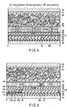
- FIG. 4 is a cross-sectional view of the liquid crystal display panel 11 taken along line A-A' in FIG. 3 .
- FIG. 5 is a cross-sectional view of the liquid crystal display panel 11 taken along line B-B' in FIG. 3 .
- the liquid crystal display panel 11 includes a COM film substrate (an opposing substrate) 30, a liquid crystal layer 32, and a TFT film substrate 33.
- the COM film substrate 30 is a substrate on which the common electrode 31 is formed.
- the TFT film substrate 33 is a substrate on which the TFT 17 is formed.
- the COM film substrate 30 is arranged opposite to the TFT film substrate 33.
- the liquid crystal layer 32 is provided between the COM film substrate 30 and the TFT film substrate 33.
- the liquid crystal layer 32 is sealed with a sealing member (not shown) for laminating the COM film substrate 30 and the TFT film substrate 33.
- the COM film substrate 30 is arranged on a display surface front side.
- the TFT film substrate 33 is arranged on a display surface back side. That is, an incident light enters the liquid crystal display panel 11 from the COM film substrate 30 side.
- a film containing PI polyimide
- As the COM film substrate 30 a transparent film containing PET (polyethylene terephthalate) is used. Details of the TFT film substrate 33 and the COM film substrate 30 will be described later.
- the liquid crystal layer 32 is constituted by a polymer dispersed liquid crystal (PDLC).
- PDLC has a structure in which a liquid crystal is dispersed by a polymer, that is, a liquid crystal is phase separated in a polymer.
- a polymer layer for example, a photocurable resin is used.
- the liquid crystal layer 32 is configured so that a refractive index of the polymer layer and a refractive index of the liquid crystal are approximately the same when an electric field is applied.
- a liquid crystal for example, a nematic liquid crystal having positive dielectric anisotropy is used.
- the liquid crystal layer 32 may be constituted by a polymer network liquid crystal (PNLC).
- PNLC polymer network liquid crystal
- PNLC has a structure in which a liquid crystal is dispersed in a polymer network. Liquid crystals in the polymer network have a continuous phase in at least some networks.
- the thickness (cell gap) of the liquid crystal layer 32 is, for example, about 7 ⁇ m. A specific configuration of the liquid crystal layer 32 will be described later.
- the common electrode 31 is provided on the liquid crystal layer 32 side of the COM film substrate 30, the common electrode 31 is provided.
- the common voltage Vcom is applied to the common electrode 31 by the common voltage supply circuit 14.
- the common electrode 31 is constituted of a transparent electrode, and for example, ITO (indium tin oxide) is used.
- the film thickness of the common electrode 31 is, for example, 10 nm or more and 200 nm or less.
- an insulating film 41 is provided on the liquid crystal layer 32 side of the TFT film substrate 33.
- the insulating film 41 for example, a silicon nitride film (SiN) or a silicon oxide film is used.
- the thickness of the insulating film 41 is, for example, 100 nm or more and 1000 nm or less. If the insulating film 41 is provided on the TFT film substrate 33, the same manufacturing processes as those in the case of using a normal glass substrate can be used for subsequent manufacturing processes.
- the insulating film 41 serves as a barrier film for the TFT film substrate 33. That is, the insulating film 41 has functions of preventing the subsequent processes from affecting the TFT film substrate 33 and blocking gas exiting from the TFT film substrate 33.
- the scanning line (wiring layer) GL extending in the X direction is provided.
- a gate insulating film 42 is provided on the scanning line GL.
- the signal line (wiring layer) SL and the TFT 17 are provided on the gate insulating film 42.
- the signal line SL extends in the Y direction.
- the TFT 17 includes the scanning line GL, the gate insulating film 42, a semiconductor layer 17A, a drain electrode 17B, and a source electrode 17C.
- the semiconductor layer 17A is provided on the gate insulating film 42 so as to be opposed to the scanning line GL.
- the drain electrode 17B is provided at one end of the semiconductor layer 17A in the Y direction, and the source electrode 17C is provided at the other end, so that each is in contact with the semiconductor layer 17A.
- the drain electrode 17B has a convex portion extending in the Y direction, and a contact plug 37 is provided on the convex portion.
- the source electrode 17C extends in the X direction, and is electrically connected to the signal line SL.
- each of the TFTs 17 for driving the pixels 16A, 16B, and 16C is arranged so as to overlap the pixel electrode 39 included in the pixel 16 adjacent in the Y direction, for example.
- the storage capacitance electrode 34 is provided on the insulating film 43.
- the storage capacitance electrode 34 is provided in the entire pixel array, except for a region through which the contact plug 37 passes.
- the storage capacitance electrode 34 functions as one electrode of the storage capacitance CS shown in FIG. 2 .
- the common voltage Vcom is supplied to the storage capacitance electrode 34 by the common voltage supply circuit 14.
- the storage capacitance electrode 34 is constituted of a transparent electrode, and for example, ITO is used.
- the reflective film 35 is provided on the storage capacitance electrode 34.
- the reflective film 35 is provided for each pixel 16. A specific configuration of the reflective film 35 will be described later.
- the reflective film 35 is configured to be electrically connected to the storage capacitance electrode 34.
- the reflective film 35 for example, aluminum (Al), silver (Ag), molybdenum (Mo), or an alloy containing any of these is used.
- An insulating film 36 is provided on the storage capacitance electrode 34 and the reflective film 35.
- an electrode 38 is provided for each pixel 16.
- the electrode 38 extends in the Y direction, and is electrically connected to the drain electrode 17B via the contact plug 37 at a Y direction end portion.
- the contact plug 37 may be formed integrally with the electrode 38, or the contact plug 37 and the electrode 38 may be separately formed.
- the electrode 38 has a function of electrically connecting the drain electrode 17B and the pixel electrode 39, and a function of setting the capacitance of the storage capacitance CS to a predetermined value according to the size of its planar shape.
- the electrode 38 has a planar shape substantially the same size as the pixel electrode 39 in order to increase the capacitance of the storage capacitance CS.
- a plurality of color filters CF (a red filter CF (R), a green filter CF (G), and a blue filter CF (B)) are provided on the electrode 38.
- a contact hole 20 is provided at the central portion of the color filter CF corresponding to each pixel 16.
- the pixel electrode 39 is provided for each pixel 16 on the color filter CF.
- the pixel electrode 39 is electrically connected to the electrode 38 via the contact plug 39A.
- the contact plug 39A may be formed integrally with the pixel electrode 39, or the contact plug 39A and the pixel electrode 39 may be separately formed.
- a pixel voltage is applied to the pixel electrode 39 by the signal driver 13.
- the insulating films 36 and 43 for example, silicon nitride (SiN) is used.
- the electrode 38, the pixel electrode 39, the contact plug 37, and the contact plug 39A are constituted of transparent electrodes, and for example, ITO is used.
- a film made from PI is used as the TFT film substrate 33.
- PI polyimide
- XENOMAX registered trademark
- the TFT film substrate 33 a transparent film made from PET (polyethylene terephthalate) is used.
- the film is formed by molding a polymer component such as a synthetic resin into a thin film shape.
- the TFT film substrate 33 is formed by molding a resin containing PI into a thin film shape
- the COM film substrate 30 is formed by molding a resin containing PET into a thin film shape.
- FIG. 6 is a diagram showing characteristics of the TFT film substrate 33 and the COM film substrate 30.
- the TFT film substrate 33 has the following characteristics: the heat resistance is 300 °C, the coefficient of thermal expansion is 5 ⁇ 10 -6 /°C or less, the transmittance is unspecified, the thickness is 5 to 50 ⁇ m, and the barrier property is unspecified.
- the adhesive strength of an adhesive material (e.g., a silane coupling material) applied to the TFT film substrate 33 is 0.01 to 1 N/cm.
- the COM film substrate (with ITO) 30 has the following characteristics: the heat resistance is 100 °C, the transmittance is 80% or more with respect to a visible light region, the thickness is 10 to 200 ⁇ m, the barrier property is 10 -4 g/m 2 /day, and the adhesive strength of an adhesive material (e.g., a silane coupling material) is 0.01 to 1 N/cm.
- the heat resistance is 100 °C
- the transmittance is 80% or more with respect to a visible light region
- the thickness is 10 to 200 ⁇ m
- the barrier property is 10 -4 g/m 2 /day
- the adhesive strength of an adhesive material e.g., a silane coupling material
- the reason for setting the heat resistance to the above temperature is as follows.
- the highest heat is applied in the film forming process. Since the temperature of this film forming process is close to 300 °C, the heat resistance of the film is set to 300 °C or higher.
- the heat resistance is normally set to 100°C or higher and to 240°C or higher in the case of using the alignment film.
- the reason for setting the coefficient of thermal expansion to the above is as follows. For example, in the case where a pattern of 100 ⁇ m is formed on the TFT film substrate 33 or the COM film substrate 30, if the maximum is 0.2 ⁇ m (500°C) in the TFT film substrate 33 and the maximum is 2.5 ⁇ m (250°C) in the COM film substrate 30, there is no problem in the manufacturing process. Therefore, the coefficient of thermal expansion of the TFT film substrate 33 is set to 5 ⁇ 10 -6 /°C or less.
- the thickness of the TFT film substrate 33 is set to 5 to 50 ⁇ m, and the thickness of the COM film substrate 30 is set to 10 to 200 ⁇ m.
- the reason for setting the barrier property to the above is as follows.
- the COM film substrate 30 needs the barrier property of 10 -4 g/m 2 /day.
- the insulating film 41 serves as a barrier.
- the adhesive material is, for example, a silane coupling material or an acrylic resin.
- the adhesive material is used for adhering the TFT film substrate 33 and the COM film substrate 30 to the glass substrate in the manufacturing process of the liquid crystal display device to be described later. Since the glass substrate is peeled off from the TFT film substrate 33 and the COM film substrate 30 after undergoing the manufacturing process of the liquid crystal display device, it is preferable that the adhesive material is basically weakly adhesive, but the edge portion is preferably strongly adhesive. Therefore, the adhesive strength of the adhesive material is 0.01 to 1 N/cm.
- a specific configuration of the liquid crystal layer 22 will be described first with reference to FIG. 4 , and then an operation of the liquid crystal display device 10 will be described.
- the liquid crystal layer 32 includes a polymer layer 32A and a liquid crystal layer 32B.
- the liquid crystal layer 32B includes liquid crystal molecules 32C.
- the liquid crystal layer 32 is constituted of a polymer dispersed liquid crystal (PDLC) or a polymer network liquid crystal (PNLC).
- PDLC has a structure in which the liquid crystal 32B is dispersed in the polymer layer (polymer network) 32A, that is, a structure in which the liquid crystal 32B is phase-separated in the polymer layer 32A.
- the liquid crystal 32B in the polymer layer 32A may have a continuous phase.
- a photocurable resin can be used as the polymer layer 32A.
- a solution obtained by mixing a liquid crystal with a photopolymerization type polymer precursor (monomer) is irradiated with ultraviolet light to polymerize a monomer to form a polymer, and the liquid crystal is dispersed in the network of the polymer.
- a nematic liquid crystal having positive (positive type) dielectric anisotropy is used as the liquid crystal 32B.
- the display operation of the liquid crystal display device 10 is controlled by the control circuit 15.
- the control circuit 15 controls the scanning driver 12, the signal driver 13, and the common voltage supply circuit 14, and applies a voltage between the pixel electrode 39 and the common electrode 31.
- the refractive index of the polymer layer 32A is different from the refractive index of the liquid crystal layer 32B
- an incident light from the COM film substrate 30 side is scattered in the liquid crystal layer 32 (a scattering state).
- the incident light in the scattering state is reflected by the reflective film 35, and a scattered light is radiated from the COM film substrate 30.
- the liquid crystal layer 32 is observed as an opaque white turbid state, the display which is visible on the observer's side is a white display.
- the color filter CF is arranged on the TFT film substrate 33 side, a color display according to the color of the color filter CF is obtained.
- an electric field is applied to the liquid crystal layer 32 (an ON state), that is, when a voltage difference (for example, a positive voltage to the pixel electrode 39 and 0 V to the common electrode 31) is applied to the pixel electrode 39 and the common electrode 31, the major axis of the liquid crystal molecules 32 C is oriented in the electric field direction (i.e., the vertical direction).
- the refractive index of the polymer layer 32A is substantially the same as the refractive index of the liquid crystal layer 32B, an incident light from the COM film substrate 30 side passes through the liquid crystal layer 32.
- the incident light that has passed through the liquid crystal layer 32 is reflected by the reflective film 35, and a mirror surface light (a specular reflection light) is radiated from the COM film substrate 30.
- a display light other than the specular reflection light is not radiated, the display which is visible on the observer's side is a black display (a dark display).
- the COM substrate and the TFT substrate are constituted of a film, it is possible to provide a liquid crystal display device which is flexible and resistant to damage.
- a display device using a polymer dispersed liquid crystal has a structure in which a TFT substrate on which a TFT is formed and a COM substrate on which a common electrode is formed sandwich the polymer dispersed liquid crystal, and a reflective film and a color filter are formed on the TFT substrate side. Since such a liquid crystal display device does not require a polarizing plate unlike a display using a normal liquid crystal, a bright reflective display is possible. Therefore, as a reflection type color liquid crystal display device, it can be used for portable electronic books, electronic dictionaries, or wearable devices which require high visibility outdoors.
- the COM substrate and the TFT substrate are made from glass. Therefore, when used as, for example, an electronic book, an electronic dictionary, or a wearable device, there may be a problem that the COM glass substrate and the TFT glass substrate sandwiching the liquid crystal layer are broken.
- the COM film substrate and the TFT film substrate are constituted of a film, these film substrates have flexibility, which may make the manufacturing process difficult.
- FIG. 7 shows a cross section of the TFT film substrate 33
- FIG. 8 shows a cross section of the COM film substrate 30.
- the TFT film substrate 33 is composed of a film containing PI.
- the thickness of the TFT film substrate 33 is, for example, 5 to 50 ⁇ m, and is 38 ⁇ m herein.
- a silane coupling material 50 is adhered on one main surface of the TFT film substrate 33.
- the silane coupling material 50 is used for adhering the TFT film substrate 33 and a glass substrate for supporting this TFT film substrate 33.
- the thickness of the silane coupling material 50 is, for example, 100 nm or less, and is 10 nm herein.
- the COM film substrate 30 is composed of a film containing PET.
- the thickness of the COM film substrate 30 is, for example, 10 to 200 ⁇ m.
- a silane coupling material 51 is adhered on one main surface of the COM film substrate 30, .
- the silane coupling material 51 is used for adhering the COM film substrate 30 and a glass substrate for supporting this COM film substrate 30.
- the thickness of the silane coupling material 51 is, for example, 100 nm or less, and is 10 nm herein.
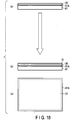
- FIGS. 9 to 13 are diagrams showing manufacturing processes for the TFT film substrate 33.
- FIGS. 9 (a), 10 (a) , 11, 12 (a) , 13 (a), and 13 (b) are side views
- FIGS. 9 (b), 10 (b) , 12 (b) , and 13 (c) are plan views.
- the TFT film substrate 33 shown in FIG. 7 is attached to a glass substrate 52.
- the TFT film substrate 33 with the silane coupling material 50 is attached to the glass substrate 52 by a roller 53.
- the silane coupling material 50 adheres the TFT film substrate 33 and the glass substrate 52.
- a black tape 54 is attached to edge portions of the surface of the glass substrate 52 to which the TFT film substrate 33 is not adhered.
- UV light (ultraviolet light) 55 is applied from the side of the surface of the glass substrate 52 to which the black tape 54 is attached. At this time, the black tape 54 blocks the UV light 55.
- the black tape 54 is peeled off from the glass substrate 52. Thereby, a region (weak adhesive portion) to which the black tape 54 is not attached is irradiated with the UV light 55, and thus becomes more weakly adhesive than a region (strong adhesive portion) 50A to which the black tape 54 is attached.
- the weak adhesive portion is, for example, 0.5 N/cm or less (preferably, 0.1 N/cm or less), and the strong adhesive portion 50A is 0.5 to 1 N/cm.
- the adhesive strength of the weak adhesive portion and the strong adhesive portion has a negative correlation with intensity and irradiation time of the UV light 55.
- FIGS. 13 (a), 13 (b), and 13 (c) the manufacturing process of the insulating film 41 and the subsequent processes shown in FIG. 4 are performed on the TFT film substrate 33 to form the pixel electrode 39.
- a plurality of cells 10A are formed on the TFT film substrate 33.
- the cell 10A is a member of a middle process before the liquid crystal display device 10 is completed.
- FIGS. 14 to 18 are diagrams showing manufacturing processes for the COM film substrate 30.
- FIGS. 14 (a), 15 (a) , 16, 17 (a) , 18 (a), and 18 (b) are side views
- FIGS. 14 (b), 15 (b) , 17 (b) , and 18 (c) are plan views.
- the COM film substrate 30 shown in FIG. 8 is attached to the glass substrate 61.
- the COM film substrate 30 with the silane coupling material 51 is attached to the glass substrate 61 by the roller 53.
- the silane coupling material 51 adheres the COM film substrate 30 and the glass substrate 61.
- the black tape 62 is attached to edge portions of the surface of the glass substrate 61 to which the COM film substrate 30 is not adhered. Subsequently, as shown in FIG. 16 , the UV light 55 is applied from the side of the surface of the glass substrate 61 to which the black tape 62 is attached. At this time, the black tape 62 blocks the UV light 55.
- the black tape 62 is peeled off from the glass substrate 61. Thereby, a region (weak adhesive portion) to which the black tape 62 is not attached is irradiated with the UV light 55, and thus becomes more weakly adhesive than a region (strong adhesive portion) to which the black tape 62 is attached.
- the weak adhesive portion is, for example, 0.5 N/cm or less (preferably, 0.1 N/cm or less), and the strong adhesive portion is 0.5 to 1 N/cm.
- the adhesive strength of the weak adhesive portion and the strong adhesive portion has a negative correlation with intensity and irradiation time of the UV light 55.
- FIGS. 18 (a), 18 (b), and 18 (c) the manufacturing process of the common electrode 31 and the subsequent processes shown in FIG. 4 are performed on the COM film substrate 30.
- the manufacturing process for the COM film substrate 30 is completed.
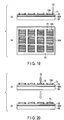
- FIGS. 19 to 23 are diagrams showing a process of manufacturing the liquid crystal display device 10 by combining the TFT film substrate 33 and the COM film substrate 30.
- FIGS. 19 (a), 20 (a), 20 (b) , 21 (a), 21 (b), 22 , 23 (a), 23 (b), and 23 (c) are side views, and
- FIG. 19 (b) is a plan view.
- On the TFT film substrate 33 a plurality of cells 10A are arranged.
- a seal member 71 and a cross member 72 are formed. Specifically, as shown in FIGS. 19 (a) and 19 (b) , the seal member 71 is discharged by a dispenser 70 for each cell 10A on the TFT film substrate 33. Subsequently, the cross member 72 is discharged for each cell 10A by the dispenser 70. The seal member 71 surrounds the cell 10A, and encloses the liquid crystal. The cross member 72 makes the common electrode 31 on the COM film substrate 30 conductive with the wiring on the TFT film substrate 33.
- a liquid crystal 73 is supplied for each cell 10A on the TFT film substrate 33. Specifically, as shown in FIG. 20 (a) , for each cell 10A, the liquid crystal 73 is dropped into its seal member 71 by the dispenser 70. Thereafter, as shown in FIG. 20 (b) , the liquid crystal 73 spreads in the seal member 71.
- the TFT film substrate 33 shown in FIG. 20 (b) and the COM film substrate 30 shown in FIG. 18 (b) are put together.
- the UV light 55 is applied from the COM film substrate 30 side.
- the monomer in the liquid crystal 73 is polymerized to constitute the polymer dispersed liquid crystal, and the seal member 71 is provisionally cured.
- FIG. 23 (a) a scribe line is drawn on the COM film substrate 30 and the TFT film substrate 33 shown in FIG. 22 by a wheel 74 for scribing. Subsequently, as shown in FIG. 23 (b) , the substrates are separated for each cell 10A. Furthermore, as shown in FIG. 23 (c) , the glass substrates 61 and 52 are peeled off from the COM film substrate 30 and the TFT film substrate 33, respectively. Through the above processes, the liquid crystal display device 10 is manufactured.
- the COM film substrate 30 and the TFT film substrate 33 with the glass substrates adhered thereto are separated for each cell 10A, and then the glass substrates are peeled off, but the glass substrates 61 and 52 may be peeled off from the COM film substrate 30 and the TFT film substrate 33 first, and then be separated for each cell 10A.
- the COM film substrate 30, and the TFT film substrate 33 having flexibility are supported by the glass substrates so that manufacturing processes using a normal glass substrate can be used as they are. This makes it possible to eliminate difficulties in the manufacturing processes.
- the present invention is not limited to the above-described embodiment, but can be embodied by modifying structural elements without departing from the gist thereof.
- the above-described embodiment includes inventions in various stages, and various inventions can be constituted by appropriately combining a plurality of structural elements disclosed in one embodiment or appropriately combining structural elements disclosed in different embodiments. For example, even if some structural elements are deleted from all the structural elements disclosed in the embodiments, the problem to be solved by the invention can be solved, and in the case where the effect of the invention can be obtained, an embodiment from which these structural elements are deleted can be extracted as an invention.
Landscapes
- Physics & Mathematics (AREA)
- Nonlinear Science (AREA)
- Chemical & Material Sciences (AREA)
- Mathematical Physics (AREA)
- Crystallography & Structural Chemistry (AREA)
- General Physics & Mathematics (AREA)
- Optics & Photonics (AREA)
- Liquid Crystal (AREA)
- Engineering & Computer Science (AREA)
- Manufacturing & Machinery (AREA)
- Dispersion Chemistry (AREA)
Abstract
Description
- The present invention generally relates to a liquid crystal display device, and more particularly to a liquid crystal display device using a polymer dispersed liquid crystal and a manufacturing method thereof.
- A polymer dispersed liquid crystal has a structure in which liquid crystals are phase separated in a three-dimensional net-like polymer (polymer network), and a light scattering state and a light transmission state are respectively created in a state in which liquid crystal molecules are randomly arranged along a side wall of the polymer network and in a state in which liquid crystal molecules are aligned in the direction of an electric field by applying the electric field.
- A display device using the polymer dispersed liquid crystal has a structure in which a TFT (Thin Film Transistor) glass substrate, on which a TFT is formed, and a COM glass substrate, on which a common electrode is formed, sandwich a polymer liquid crystal, and a reflective film and a color filter are formed on the TFT glass substrate side (for example, Jpn. Pat. Appln. KOKAI Publication No.
2015-82018 - However, when used as an electronic book, an electronic dictionary, or a wearable device, the glass substrate constituting the liquid crystal display device is liable to be damaged.
- An object of the present invention is to provide a liquid crystal display device which is flexible and resistant to damage and a method of manufacturing the same.
- A liquid crystal display device according to an aspect of the present invention is characterized by comprising: a first film substrate having flexibility; a second film substrate having flexibility and arranged so as to be opposed to the first film substrate; a liquid crystal layer including a polymer dispersed liquid crystal (PDLC) or a polymer network type liquid crystal (PNLC) and sandwiched between the first film substrate and the second film substrate; a switching element provided on the first film substrate; a reflective film provided on the switching element; a pixel electrode provided on the reflective film and electrically connected to a drain electrode of the switching element; and a common electrode provided on the second film substrate.
- A manufacturing method of a liquid crystal display device according to an aspect of the present invention is characterized by comprising: attaching a first film substrate to a first glass substrate; forming a switching element, a reflective film, and a color filter on the first film substrate adhered to the first glass substrate; attaching a second film substrate to a second glass substrate; and combining the first glass substrate with the first film substrate and the second glass substrate with the second film substrate and filling a polymer dispersed liquid crystal or a polymer network liquid crystal in between the first film substrate and the second film substrate.
- According to the present invention, it is possible to provide a liquid crystal display device which is flexible and resistant to damage, and a manufacturing method thereof.
-
-
FIG. 1 is a block diagram of a liquid crystal display device according to an embodiment. -
FIG. 2 is a circuit diagram of a pixel in the liquid crystal display device. -
FIG. 3 is a layout diagram of a liquid crystal display panel in the embodiment. -
FIG. 4 is a cross-sectional view of the liquid crystal display panel taken along line A-A' inFIG. 3 . -
FIG. 5 is a cross-sectional view of the liquid crystal display panel taken along line B-B' inFIG. 3 . -
FIG. 6 is a diagram showing characteristics of a TFT film substrate and a COM film substrate in the embodiment. -
FIG. 7 is a cross-sectional view of the TFT film substrate in the embodiment. -
FIG. 8 is a cross-sectional view of the COM film substrate in the embodiment. -
FIG. 9 is a view showing a manufacturing process of the TFT film substrate in the embodiment. -
FIG. 10 is a view showing the manufacturing process of the TFT film substrate in the embodiment. -
FIG. 11 is a view showing the manufacturing process of the TFT film substrate in the embodiment. -
FIG. 12 is a view showing the manufacturing process of the TFT film substrate in the embodiment. -
FIG. 13 is a view showing the manufacturing process of the TFT film substrate in the embodiment. -
FIG. 14 is a view showing a manufacturing process of a COM film substrate in the embodiment. -
FIG. 15 is a view showing the manufacturing process of the COM film substrate in the embodiment. -
FIG. 16 is a view showing the manufacturing process of the COM film substrate in the embodiment. -
FIG. 17 is a view showing the manufacturing process of the COM film substrate in the embodiment. -
FIG. 18 is a view showing the manufacturing process of the COM film substrate in the embodiment. -
FIG. 19 is a view showing a process of manufacturing the liquid crystal display device by combining the TFT film substrate and the COM film substrate in the embodiment. -
FIG. 20 is a view showing the process of manufacturing the liquid crystal display device by combining the TFT film substrate and the COM film substrate in the embodiment. -
FIG. 21 is a view showing the process of manufacturing the liquid crystal display device by combining the TFT film substrate and the COM film substrate in the embodiment. -
FIG. 22 is a view showing the process of manufacturing the liquid crystal display device by combining the TFT film substrate and the COM film substrate in the embodiment. -
FIG. 23 is a view showing the process of manufacturing the liquid crystal display device by combining the TFT film substrate and the COM film substrate in the embodiment. - Hereinafter, embodiments will be described with reference to the drawings. It should be noted that the drawings are schematic or conceptual, and the dimensions and ratios of the drawings are not necessarily the same as the actual ones. In addition, even when the same parts are shown in the drawings, their dimensional relationships and ratios may be illustrated differently from one another. In particular, some embodiments described below exemplify apparatuses and methods for embodying the technical idea of the present invention, and the technical idea of the present invention is not specified depending on the shape, structure, arrangement, etc. of constituent components. In the following descriptions, elements having the same functions and configurations are denoted by the same reference numerals, and redundant explanations are given only when necessary.
- Hereinafter, a liquid crystal display device of an embodiment will be described.
-
FIG. 1 is a block diagram of a liquid crystal display device according to an embodiment. A liquidcrystal display device 10 includes a liquidcrystal display panel 11, a scanning driver (a scanning line driving circuit) 12, a signal driver (a signal line driving circuit) 13, a commonvoltage supply circuit 14, and acontrol circuit 15. - In the liquid
crystal display panel 11, a plurality of scanning lines GL each extending in the row direction (X direction) and a plurality of signal lines SL each extending in the column direction (Y direction) are arranged. In each intersection region between the plurality of scanning lines GL and the plurality of signal lines SL, apixel 16 is arranged. The plurality ofpixels 16 are arranged in a matrix. -
FIG. 2 is a circuit diagram of onepixel 16. Thepixel 16 includes aswitching element 17, a liquid crystal capacitance CLC, and a storage capacitance CS. The switchingelement 17 is composed of, for example, a thin film transistor (TFT). - A source of a
TFT 17 is electrically connected to the signal line SL. A gate of the TFT 17 is electrically connected to the scanning line GL. A drain of theTFT 17 is electrically connected to a pixel electrode. The pixel electrode constitutes a liquid crystal capacitance CLC together with a common electrode arranged opposite to the pixel electrode and liquid crystal sandwiched between the pixel electrode and the common electrode. - The storage capacitance CS is connected in parallel with the liquid crystal capacitance CLC. The storage capacitance CS suppresses a potential fluctuation occurring in the pixel electrode, and maintains a pixel voltage applied to the pixel electrode until the next pixel voltage is applied again. The storage capacitance CS is composed of a storage electrode arranged opposite to the pixel electrode and an insulating film formed between the pixel electrode and the storage electrode. A common voltage Vcom is applied to the common electrode and the storage electrode by the common
voltage supply circuit 14. - In the
pixel 16 configured as described above, when theTFT 17 connected to the pixel electrode is turned on, the pixel voltage is applied to the pixel electrode via the signal line SL, and an alignment state of the liquid crystal is changed according to a voltage difference between the pixel voltage and the common voltage Vcom. As a result, a transmission state of the liquid crystal with respect to an incident light and a reflected light is changed, and image display is performed. - The
scanning driver 12 is connected to the plurality of scanning lines GL, and sequentially drives the plurality of scanning lines GL based on a vertical control signal from thecontrol circuit 15. The vertical control signal from thecontrol circuit 15 is applied every one frame period. "Frame" is a period during which one image is displayed by supplying display signals to all the pixels of the liquid crystal display panel. - The
signal driver 13 is connected to the plurality of signal lines SL, and fetches image data for one horizontal period based on a horizontal control signal from thecontrol circuit 15. The horizontal control signal from thecontrol circuit 15 is generated every horizontal period which is a period for transferring a display signal for one row (one scanning line) of the liquidcrystal display panel 11 to the pixels. Then, thesignal driver 13 supplies a display signal corresponding to the image data to the pixel electrode via the signal line SL. - The
control circuit 15 generates various control signals for displaying a desired image on the liquidcrystal display panel 11 based on the image data supplied from the outside, and supplies the control signals to thescanning driver 12, thesignal driver 13, and the commonvoltage supply circuit 14. - Generally, in a liquid crystal display device, inversion driving (AC driving) is performed in which the polarity of an electric field between a pixel electrode and a common electrode sandwiching the liquid crystal is inverted at a predetermined period. In the liquid
crystal display panel 11, as described above, the arrangement of the liquid crystal is determined according to the electric field between the pixel electrode and the common electrode. However, if an electric field of the same polarity is continuously applied between the pixel electrode and the common electrode, it may cause image burn-in or deterioration and destruction of the liquid crystal. Therefore, by periodically inverting the polarity of the electric field between the pixel electrode and the common electrode, deterioration of the liquid crystal, etc. is prevented. As an inversion driving method, line inversion driving and frame inversion driving are common. The line inversion driving is a method of inverting the polarity of an electric field for each scanning line and also inverting it for each frame period. The frame inversion driving is a method of inverting the polarity of an electric field for each pixel for each frame period. - The liquid
crystal display panel 11 is constituted of a reflective type color PDLCD (Polymer Dispersed Liquid Crystal Display). The liquidcrystal display panel 11 uses an active matrix method in which active elements are arranged for eachpixel 16. In the present embodiment, end portions of adjacent color filters CF are overlapped, and a reflective film is provided independently for eachpixel 16. -
FIG. 3 is a layout diagram of the liquidcrystal display panel 11 according to the embodiment. InFIG. 3 , threepixels crystal display panel 11 are extracted and shown. The liquidcrystal display panel 11 further includes a plurality of pixels in such a manner that the pixels shown inFIG. 3 are repeated in the X direction and in the Y direction orthogonal to the X direction. The width of a space between thepixel electrodes 39 adjacent in the X direction is denoted as d1, and the width of a space between thepixel electrodes 39 adjacent in the Y direction is denoted as d2. InFIG. 3 , areflective film 35 and astorage capacitance electrode 34 are not shown in order to avoid complication of the drawing. -
FIG. 4 is a cross-sectional view of the liquidcrystal display panel 11 taken along line A-A' inFIG. 3 .FIG. 5 is a cross-sectional view of the liquidcrystal display panel 11 taken along line B-B' inFIG. 3 . As shown inFIGS. 4 and 5 , the liquidcrystal display panel 11 includes a COM film substrate (an opposing substrate) 30, aliquid crystal layer 32, and aTFT film substrate 33. TheCOM film substrate 30 is a substrate on which thecommon electrode 31 is formed. TheTFT film substrate 33 is a substrate on which theTFT 17 is formed. - The
COM film substrate 30 is arranged opposite to theTFT film substrate 33. Theliquid crystal layer 32 is provided between theCOM film substrate 30 and theTFT film substrate 33. Theliquid crystal layer 32 is sealed with a sealing member (not shown) for laminating theCOM film substrate 30 and theTFT film substrate 33. TheCOM film substrate 30 is arranged on a display surface front side. TheTFT film substrate 33 is arranged on a display surface back side. That is, an incident light enters the liquidcrystal display panel 11 from theCOM film substrate 30 side. As theTFT film substrate 33, a film containing PI (polyimide) is used. As theCOM film substrate 30, a transparent film containing PET (polyethylene terephthalate) is used. Details of theTFT film substrate 33 and theCOM film substrate 30 will be described later. - The
liquid crystal layer 32 is constituted by a polymer dispersed liquid crystal (PDLC). PDLC has a structure in which a liquid crystal is dispersed by a polymer, that is, a liquid crystal is phase separated in a polymer. As a polymer layer (polymer layer), for example, a photocurable resin is used. Theliquid crystal layer 32 is configured so that a refractive index of the polymer layer and a refractive index of the liquid crystal are approximately the same when an electric field is applied. As a liquid crystal, for example, a nematic liquid crystal having positive dielectric anisotropy is used. Theliquid crystal layer 32 may be constituted by a polymer network liquid crystal (PNLC). PNLC has a structure in which a liquid crystal is dispersed in a polymer network. Liquid crystals in the polymer network have a continuous phase in at least some networks. The thickness (cell gap) of theliquid crystal layer 32 is, for example, about 7 µm. A specific configuration of theliquid crystal layer 32 will be described later. - On the
liquid crystal layer 32 side of theCOM film substrate 30, thecommon electrode 31 is provided. The common voltage Vcom is applied to thecommon electrode 31 by the commonvoltage supply circuit 14. Thecommon electrode 31 is constituted of a transparent electrode, and for example, ITO (indium tin oxide) is used. The film thickness of thecommon electrode 31 is, for example, 10 nm or more and 200 nm or less. - On the
liquid crystal layer 32 side of theTFT film substrate 33, an insulatingfilm 41 is provided. As the insulatingfilm 41, for example, a silicon nitride film (SiN) or a silicon oxide film is used. The thickness of the insulatingfilm 41 is, for example, 100 nm or more and 1000 nm or less. If the insulatingfilm 41 is provided on theTFT film substrate 33, the same manufacturing processes as those in the case of using a normal glass substrate can be used for subsequent manufacturing processes. Furthermore, the insulatingfilm 41 serves as a barrier film for theTFT film substrate 33. That is, the insulatingfilm 41 has functions of preventing the subsequent processes from affecting theTFT film substrate 33 and blocking gas exiting from theTFT film substrate 33. - On the insulating
film 41, the scanning line (wiring layer) GL extending in the X direction is provided. On the scanning line GL, agate insulating film 42 is provided. On thegate insulating film 42, the signal line (wiring layer) SL and theTFT 17 are provided. The signal line SL extends in the Y direction. - The
TFT 17 includes the scanning line GL, thegate insulating film 42, asemiconductor layer 17A, adrain electrode 17B, and asource electrode 17C. Thesemiconductor layer 17A is provided on thegate insulating film 42 so as to be opposed to the scanning line GL. Thedrain electrode 17B is provided at one end of thesemiconductor layer 17A in the Y direction, and thesource electrode 17C is provided at the other end, so that each is in contact with thesemiconductor layer 17A. Thedrain electrode 17B has a convex portion extending in the Y direction, and acontact plug 37 is provided on the convex portion. The source electrode 17C extends in the X direction, and is electrically connected to the signal line SL. As thesemiconductor layer 17A, for example, amorphous silicon is used. As thegate insulating film 42, for example, silicon nitride (SiN) is used. As shown inFIG. 3 , each of theTFTs 17 for driving thepixels pixel electrode 39 included in thepixel 16 adjacent in the Y direction, for example. - An insulating
film 43 is provided on the signal line SL and theTFT 17. Thestorage capacitance electrode 34 is provided on the insulatingfilm 43. Thestorage capacitance electrode 34 is provided in the entire pixel array, except for a region through which the contact plug 37 passes. Thestorage capacitance electrode 34 functions as one electrode of the storage capacitance CS shown inFIG. 2 . The common voltage Vcom is supplied to thestorage capacitance electrode 34 by the commonvoltage supply circuit 14. Thestorage capacitance electrode 34 is constituted of a transparent electrode, and for example, ITO is used. - The
reflective film 35 is provided on thestorage capacitance electrode 34. Thereflective film 35 is provided for eachpixel 16. A specific configuration of thereflective film 35 will be described later. In the present embodiment, as shown inFIGS. 4 and 5 , thereflective film 35 is configured to be electrically connected to thestorage capacitance electrode 34. As thereflective film 35, for example, aluminum (Al), silver (Ag), molybdenum (Mo), or an alloy containing any of these is used. - An insulating
film 36 is provided on thestorage capacitance electrode 34 and thereflective film 35. On the insulatingfilm 36, anelectrode 38 is provided for eachpixel 16. Theelectrode 38 extends in the Y direction, and is electrically connected to thedrain electrode 17B via thecontact plug 37 at a Y direction end portion. Thecontact plug 37 may be formed integrally with theelectrode 38, or thecontact plug 37 and theelectrode 38 may be separately formed. Theelectrode 38 has a function of electrically connecting thedrain electrode 17B and thepixel electrode 39, and a function of setting the capacitance of the storage capacitance CS to a predetermined value according to the size of its planar shape. Theelectrode 38 has a planar shape substantially the same size as thepixel electrode 39 in order to increase the capacitance of the storage capacitance CS. - A plurality of color filters CF (a red filter CF (R), a green filter CF (G), and a blue filter CF (B)) are provided on the
electrode 38. The color filters CF adjacent in the X direction overlap each other at the end portions. Acontact hole 20 is provided at the central portion of the color filter CF corresponding to eachpixel 16. - The
pixel electrode 39 is provided for eachpixel 16 on the color filter CF. Thepixel electrode 39 is electrically connected to theelectrode 38 via thecontact plug 39A. Thecontact plug 39A may be formed integrally with thepixel electrode 39, or the contact plug 39A and thepixel electrode 39 may be separately formed. A pixel voltage is applied to thepixel electrode 39 by thesignal driver 13. - As the insulating
films electrode 38, thepixel electrode 39, thecontact plug 37, and the contact plug 39A are constituted of transparent electrodes, and for example, ITO is used. - As described above, a film made from PI (polyimide) is used as the
TFT film substrate 33. For example, "XENOMAX" (registered trademark) is used for theTFT film substrate 33. As theCOM film substrate 30, a transparent film made from PET (polyethylene terephthalate) is used. The film is formed by molding a polymer component such as a synthetic resin into a thin film shape. TheTFT film substrate 33 is formed by molding a resin containing PI into a thin film shape, and theCOM film substrate 30 is formed by molding a resin containing PET into a thin film shape. -
FIG. 6 is a diagram showing characteristics of theTFT film substrate 33 and theCOM film substrate 30. - The
TFT film substrate 33 has the following characteristics: the heat resistance is 300 °C, the coefficient of thermal expansion is 5 × 10⁻⁶/°C or less, the transmittance is unspecified, the thickness is 5 to 50 µm, and the barrier property is unspecified. The adhesive strength of an adhesive material (e.g., a silane coupling material) applied to theTFT film substrate 33 is 0.01 to 1 N/cm. - The COM film substrate (with ITO) 30 has the following characteristics: the heat resistance is 100 °C, the transmittance is 80% or more with respect to a visible light region, the thickness is 10 to 200 µm, the barrier property is 10-4 g/m2/day, and the adhesive strength of an adhesive material (e.g., a silane coupling material) is 0.01 to 1 N/cm.
- The reason for setting the heat resistance to the above temperature is as follows. In the manufacturing process of the
TFT film substrate 33, the highest heat is applied in the film forming process. Since the temperature of this film forming process is close to 300 °C, the heat resistance of the film is set to 300 °C or higher. On the other hand, in the manufacturing process of theCOM film substrate 30, since the highest temperature to be applied is 240 °C in the case of using an alignment film (a PI film) and is 100 °C in the other cases, the heat resistance is normally set to 100°C or higher and to 240°C or higher in the case of using the alignment film. - The reason for setting the coefficient of thermal expansion to the above is as follows. For example, in the case where a pattern of 100 µm is formed on the
TFT film substrate 33 or theCOM film substrate 30, if the maximum is 0.2 µm (500°C) in theTFT film substrate 33 and the maximum is 2.5 µm (250°C) in theCOM film substrate 30, there is no problem in the manufacturing process. Therefore, the coefficient of thermal expansion of theTFT film substrate 33 is set to 5×10⁻⁶/°C or less. - In accordance with product requirements, the thickness of the
TFT film substrate 33 is set to 5 to 50 µm, and the thickness of theCOM film substrate 30 is set to 10 to 200 µm. - The reason for setting the barrier property to the above is as follows. In order to prevent water penetration into the
liquid crystal layer 32, theCOM film substrate 30 needs the barrier property of 10-4 g/m2/day. In theTFT film substrate 33, since the insulating film (silicon oxide film) 41 is first formed on the film surface, the insulatingfilm 41 serves as a barrier. - The reason for setting the adhesive strength of the adhesive material to the above is as follows. The adhesive material is, for example, a silane coupling material or an acrylic resin. The adhesive material is used for adhering the
TFT film substrate 33 and theCOM film substrate 30 to the glass substrate in the manufacturing process of the liquid crystal display device to be described later. Since the glass substrate is peeled off from theTFT film substrate 33 and theCOM film substrate 30 after undergoing the manufacturing process of the liquid crystal display device, it is preferable that the adhesive material is basically weakly adhesive, but the edge portion is preferably strongly adhesive. Therefore, the adhesive strength of the adhesive material is 0.01 to 1 N/cm. - A specific configuration of the liquid crystal layer 22 will be described first with reference to
FIG. 4 , and then an operation of the liquidcrystal display device 10 will be described. - The
liquid crystal layer 32 includes a polymer layer 32A and a liquid crystal layer 32B. The liquid crystal layer 32B includes liquid crystal molecules 32C. In detail, theliquid crystal layer 32 is constituted of a polymer dispersed liquid crystal (PDLC) or a polymer network liquid crystal (PNLC). PDLC has a structure in which the liquid crystal 32B is dispersed in the polymer layer (polymer network) 32A, that is, a structure in which the liquid crystal 32B is phase-separated in the polymer layer 32A. Alternatively, the liquid crystal 32B in the polymer layer 32A may have a continuous phase. - As the polymer layer 32A, a photocurable resin can be used. For example, in PDLC, a solution obtained by mixing a liquid crystal with a photopolymerization type polymer precursor (monomer) is irradiated with ultraviolet light to polymerize a monomer to form a polymer, and the liquid crystal is dispersed in the network of the polymer. As the liquid crystal 32B, for example, a nematic liquid crystal having positive (positive type) dielectric anisotropy is used. That is, when no voltage is applied to the
liquid crystal layer 32, it becomes a state in which the liquid crystal molecules 32C are randomly arranged in the polymer layer 32A, and when a voltage is applied to theliquid crystal layer 32, it becomes a state in which the liquid crystal molecules 32C are directed perpendicular to an electric field direction (a state in which a major axis of the liquid crystal molecule 32C is oriented toward the electric field direction). - Next, the operation of the liquid
crystal display device 10 will be described. The display operation of the liquidcrystal display device 10 is controlled by thecontrol circuit 15. Thecontrol circuit 15 controls thescanning driver 12, thesignal driver 13, and the commonvoltage supply circuit 14, and applies a voltage between thepixel electrode 39 and thecommon electrode 31. - When an electric field is not applied to the liquid crystal layer 32 (an OFF state), that is, when the
pixel electrode 39 and thecommon electrode 31 are set to the same voltage (for example, 0 V), the liquid crystal molecules 32C are randomly arranged. - In this case, since the refractive index of the polymer layer 32A is different from the refractive index of the liquid crystal layer 32B, an incident light from the
COM film substrate 30 side is scattered in the liquid crystal layer 32 (a scattering state). The incident light in the scattering state is reflected by thereflective film 35, and a scattered light is radiated from theCOM film substrate 30. At this time, since theliquid crystal layer 32 is observed as an opaque white turbid state, the display which is visible on the observer's side is a white display. Actually, since the color filter CF is arranged on theTFT film substrate 33 side, a color display according to the color of the color filter CF is obtained. - On the other hand, when an electric field is applied to the liquid crystal layer 32 (an ON state), that is, when a voltage difference (for example, a positive voltage to the
pixel electrode 39 and 0 V to the common electrode 31) is applied to thepixel electrode 39 and thecommon electrode 31, the major axis of the liquid crystal molecules 32 C is oriented in the electric field direction (i.e., the vertical direction). - In this case, since the refractive index of the polymer layer 32A is substantially the same as the refractive index of the liquid crystal layer 32B, an incident light from the
COM film substrate 30 side passes through theliquid crystal layer 32. The incident light that has passed through theliquid crystal layer 32 is reflected by thereflective film 35, and a mirror surface light (a specular reflection light) is radiated from theCOM film substrate 30. At this time, since a display light other than the specular reflection light is not radiated, the display which is visible on the observer's side is a black display (a dark display). - According to the present embodiment, since the COM substrate and the TFT substrate are constituted of a film, it is possible to provide a liquid crystal display device which is flexible and resistant to damage.
- A display device using a polymer dispersed liquid crystal has a structure in which a TFT substrate on which a TFT is formed and a COM substrate on which a common electrode is formed sandwich the polymer dispersed liquid crystal, and a reflective film and a color filter are formed on the TFT substrate side. Since such a liquid crystal display device does not require a polarizing plate unlike a display using a normal liquid crystal, a bright reflective display is possible. Therefore, as a reflection type color liquid crystal display device, it can be used for portable electronic books, electronic dictionaries, or wearable devices which require high visibility outdoors.
- However, in this liquid crystal display device, usually, the COM substrate and the TFT substrate are made from glass. Therefore, when used as, for example, an electronic book, an electronic dictionary, or a wearable device, there may be a problem that the COM glass substrate and the TFT glass substrate sandwiching the liquid crystal layer are broken.
- Therefore, in the present embodiment, by using a film for the COM substrate and the TFT substrate, it is possible to realize a liquid crystal display device in which flexibility is given to the liquid crystal panel and the liquid crystal panel is resistant to damage.
- On the other hand, if the COM film substrate and the TFT film substrate are constituted of a film, these film substrates have flexibility, which may make the manufacturing process difficult.
- Hereinafter, a manufacturing method for solving the difficulty of such a manufacturing process will be described.
- In the manufacture of the liquid
crystal display device 10, first, processes for theTFT film substrate 33 and theCOM film substrate 30 are respectively performed, and after that, a process of manufacturing the liquidcrystal display device 10 by combining theTFT film substrate 33 and theCOM film substrate 30 is performed. -
FIG. 7 shows a cross section of theTFT film substrate 33, andFIG. 8 shows a cross section of theCOM film substrate 30. - The
TFT film substrate 33 is composed of a film containing PI. The thickness of theTFT film substrate 33 is, for example, 5 to 50 µm, and is 38 µm herein. On one main surface of theTFT film substrate 33, asilane coupling material 50 is adhered. Thesilane coupling material 50 is used for adhering theTFT film substrate 33 and a glass substrate for supporting thisTFT film substrate 33. The thickness of thesilane coupling material 50 is, for example, 100 nm or less, and is 10 nm herein. - The
COM film substrate 30 is composed of a film containing PET. The thickness of theCOM film substrate 30 is, for example, 10 to 200 µm. On one main surface of theCOM film substrate 30, asilane coupling material 51 is adhered. Thesilane coupling material 51 is used for adhering theCOM film substrate 30 and a glass substrate for supporting thisCOM film substrate 30. The thickness of thesilane coupling material 51 is, for example, 100 nm or less, and is 10 nm herein. -
FIGS. 9 to 13 are diagrams showing manufacturing processes for theTFT film substrate 33.FIGS. 9 (a), 10 (a) ,11, 12 (a) ,13 (a), and 13 (b) are side views, andFIGS. 9 (b), 10 (b) ,12 (b) , and13 (c) are plan views. - First, the
TFT film substrate 33 shown inFIG. 7 is attached to aglass substrate 52. Specifically, as shown inFIG. 9 (a) , theTFT film substrate 33 with thesilane coupling material 50 is attached to theglass substrate 52 by aroller 53. Thesilane coupling material 50 adheres theTFT film substrate 33 and theglass substrate 52. - Next, as shown in
FIGS. 10 (a) and 10 (b) , ablack tape 54 is attached to edge portions of the surface of theglass substrate 52 to which theTFT film substrate 33 is not adhered. Subsequently, as shown inFIG. 11 , UV light (ultraviolet light) 55 is applied from the side of the surface of theglass substrate 52 to which theblack tape 54 is attached. At this time, theblack tape 54 blocks theUV light 55. - Thereafter, as shown in
FIGS. 12 (a) and 12 (b) , theblack tape 54 is peeled off from theglass substrate 52. Thereby, a region (weak adhesive portion) to which theblack tape 54 is not attached is irradiated with theUV light 55, and thus becomes more weakly adhesive than a region (strong adhesive portion) 50A to which theblack tape 54 is attached. The weak adhesive portion is, for example, 0.5 N/cm or less (preferably, 0.1 N/cm or less), and the strongadhesive portion 50A is 0.5 to 1 N/cm. The adhesive strength of the weak adhesive portion and the strong adhesive portion has a negative correlation with intensity and irradiation time of theUV light 55. - Thereafter, as shown in
FIGS. 13 (a), 13 (b), and 13 (c) , the manufacturing process of the insulatingfilm 41 and the subsequent processes shown inFIG. 4 are performed on theTFT film substrate 33 to form thepixel electrode 39. By the above, a plurality ofcells 10A are formed on theTFT film substrate 33. Thecell 10A is a member of a middle process before the liquidcrystal display device 10 is completed. -
FIGS. 14 to 18 are diagrams showing manufacturing processes for theCOM film substrate 30.FIGS. 14 (a), 15 (a) ,16, 17 (a) ,18 (a), and 18 (b) are side views, andFIGS. 14 (b), 15 (b) ,17 (b) , and18 (c) are plan views. - First, the
COM film substrate 30 shown inFIG. 8 is attached to theglass substrate 61. Specifically, as shown inFIG. 14 (a) , theCOM film substrate 30 with thesilane coupling material 51 is attached to theglass substrate 61 by theroller 53. Thesilane coupling material 51 adheres theCOM film substrate 30 and theglass substrate 61. - Next, as shown in
FIGS. 15 (a) and 15 (b) , theblack tape 62 is attached to edge portions of the surface of theglass substrate 61 to which theCOM film substrate 30 is not adhered. Subsequently, as shown inFIG. 16 , theUV light 55 is applied from the side of the surface of theglass substrate 61 to which theblack tape 62 is attached. At this time, theblack tape 62 blocks theUV light 55. - Thereafter, as shown in
FIGS. 17 (a) and 17 (b) , theblack tape 62 is peeled off from theglass substrate 61. Thereby, a region (weak adhesive portion) to which theblack tape 62 is not attached is irradiated with theUV light 55, and thus becomes more weakly adhesive than a region (strong adhesive portion) to which theblack tape 62 is attached. Similarly to the above-described case, the weak adhesive portion is, for example, 0.5 N/cm or less (preferably, 0.1 N/cm or less), and the strong adhesive portion is 0.5 to 1 N/cm. The adhesive strength of the weak adhesive portion and the strong adhesive portion has a negative correlation with intensity and irradiation time of theUV light 55. - Thereafter, as shown in
FIGS. 18 (a), 18 (b), and 18 (c) , the manufacturing process of thecommon electrode 31 and the subsequent processes shown inFIG. 4 are performed on theCOM film substrate 30. By the above, the manufacturing process for theCOM film substrate 30 is completed. -
FIGS. 19 to 23 are diagrams showing a process of manufacturing the liquidcrystal display device 10 by combining theTFT film substrate 33 and theCOM film substrate 30.FIGS. 19 (a), 20 (a), 20 (b) ,21 (a), 21 (b), 22 ,23 (a), 23 (b), and 23 (c) are side views, andFIG. 19 (b) is a plan view. On theTFT film substrate 33, a plurality ofcells 10A are arranged. - First, for each
cell 10A on theTFT film substrate 33 shown inFIG. 13 (b) , aseal member 71 and across member 72 are formed. Specifically, as shown inFIGS. 19 (a) and 19 (b) , theseal member 71 is discharged by adispenser 70 for eachcell 10A on theTFT film substrate 33. Subsequently, thecross member 72 is discharged for eachcell 10A by thedispenser 70. Theseal member 71 surrounds thecell 10A, and encloses the liquid crystal. Thecross member 72 makes thecommon electrode 31 on theCOM film substrate 30 conductive with the wiring on theTFT film substrate 33. - Next, a
liquid crystal 73 is supplied for eachcell 10A on theTFT film substrate 33. Specifically, as shown inFIG. 20 (a) , for eachcell 10A, theliquid crystal 73 is dropped into itsseal member 71 by thedispenser 70. Thereafter, as shown inFIG. 20 (b) , theliquid crystal 73 spreads in theseal member 71. - Next, as shown in
FIGS. 21 (a) and 21 (b) , theTFT film substrate 33 shown inFIG. 20 (b) and theCOM film substrate 30 shown inFIG. 18 (b) are put together. Subsequently, as shown inFIG. 22 , theUV light 55 is applied from theCOM film substrate 30 side. Thereby, the monomer in theliquid crystal 73 is polymerized to constitute the polymer dispersed liquid crystal, and theseal member 71 is provisionally cured. - Next, as shown in
FIG. 23 (a) , a scribe line is drawn on theCOM film substrate 30 and theTFT film substrate 33 shown inFIG. 22 by a wheel 74 for scribing. Subsequently, as shown inFIG. 23 (b) , the substrates are separated for eachcell 10A. Furthermore, as shown inFIG. 23 (c) , theglass substrates COM film substrate 30 and theTFT film substrate 33, respectively. Through the above processes, the liquidcrystal display device 10 is manufactured. - In the processes shown in
FIGS. 23 (a), 23 (b), and 23 (c) , theCOM film substrate 30 and theTFT film substrate 33 with the glass substrates adhered thereto are separated for eachcell 10A, and then the glass substrates are peeled off, but theglass substrates COM film substrate 30 and theTFT film substrate 33 first, and then be separated for eachcell 10A. - According to the above-described manufacturing method of the liquid crystal display device, the
COM film substrate 30, and theTFT film substrate 33 having flexibility are supported by the glass substrates so that manufacturing processes using a normal glass substrate can be used as they are. This makes it possible to eliminate difficulties in the manufacturing processes. - The present invention is not limited to the above-described embodiment, but can be embodied by modifying structural elements without departing from the gist thereof. Furthermore, the above-described embodiment includes inventions in various stages, and various inventions can be constituted by appropriately combining a plurality of structural elements disclosed in one embodiment or appropriately combining structural elements disclosed in different embodiments. For example, even if some structural elements are deleted from all the structural elements disclosed in the embodiments, the problem to be solved by the invention can be solved, and in the case where the effect of the invention can be obtained, an embodiment from which these structural elements are deleted can be extracted as an invention.
Claims (15)
- A liquid crystal display device comprising:a first film substrate having flexibility;a second film substrate having flexibility and arranged so as to be opposed to the first film substrate;a liquid crystal layer including a polymer dispersed liquid crystal (PDLC) or a polymer network type liquid crystal (PNLC) and sandwiched between the first film substrate and the second film substrate;a switching element provided on the first film substrate;a reflective film provided on the switching element;a pixel electrode provided on the reflective film and electrically connected to a drain electrode of the switching element; anda common electrode provided on the second film substrate.
- The liquid crystal display device according to claim 1, further comprising a color filter arranged on the switching element on the first film substrate.
- The liquid crystal display device according to claim 1, wherein the first film substrate has a heat resistance of 300°C or higher and a coefficient of thermal expansion of 5 × 10⁻⁶/°C or less.
- The liquid crystal display device according to claim 1, wherein the second film substrate has a heat resistance of 100 °C or higher and a transmittance of a visible light of 80% or more.
- The liquid crystal display device according to claim 1, wherein the second film substrate transmits light of a 300 to 400 nm waveband on a shortwave side which is outside a visible light, and has a transmittance of 20% or more in a 365 nm wavelength.
- The liquid crystal display device according to claim 1, further comprising a transparent conductive film provided on the second film substrate, the transparent conductive film having a thickness of 10 to 200 nm.
- The liquid crystal display device according to claim 1, wherein the first film substrate is made of polyimide, and the second film substrate is made of polyethylene terephthalate.
- The liquid crystal display device according to claim 1, wherein the switching element is a thin film transistor, and the thin film transistor is configured to drive the pixel electrode.
- The liquid crystal display device according to claim 1, further comprising:a wiring layer provided between the first film substrate and the switching element and electrically connected to a source electrode of the switching element; andan insulating film provided between the first film substrate and the wiring layer.
- A manufacturing method of a liquid crystal display device comprising:attaching a first film substrate to a first glass substrate;forming a switching element, a reflective film, and a color filter on the first film substrate adhered to the first glass substrate;attaching a second film substrate to a second glass substrate; andcombining the first glass substrate with the first film substrate and the second glass substrate with the second film substrate and filling a polymer dispersed liquid crystal or a polymer network liquid crystal in between the first film substrate and the second film substrate.
- The manufacturing method of a liquid crystal display device according to claim 10, wherein the first film substrate and the first glass substrate are adhered by a first adhesive material, the second film substrate and a second glass substrate are adhered by a second adhesive material, at least one of the first and second adhesive materials is a silane coupling material, and an adhesive strength of the silane coupling material is 0.01 to 1 N/cm.
- The manufacturing method of a liquid crystal display device according to claim 10, wherein the polymer dispersed liquid crystal or the polymer network liquid crystal in between the first film substrate and the second film substrate is filled in by one drop filling (ODF).
- The manufacturing method of a liquid crystal display device according to claim 10, further comprising:after filling the polymer dispersed liquid crystal or the polymer network liquid crystal, peeling off the first and second glass substrates from the first and second film substrates, respectively; andseparating the first and second film substrates from which the first and second glass substrates are peeled off into a plurality of liquid crystal display devices.
- The manufacturing method of a liquid crystal display device according to claim 10, further comprising:after filling the polymer dispersed liquid crystal or the polymer network liquid crystal, separating the first and second glass substrates and the first and second film substrates into a plurality of liquid crystal display substrates; andpeeling off the first and second glass substrates from the first and second film substrates of the liquid crystal display substrates, respectively, to form a plurality of liquid crystal display devices.
- The manufacturing method of a liquid crystal display device according to claim 10, further comprising after forming the color filter, forming a seal member on the first film substrate,
wherein the seal member seals in a periphery of the polymer dispersed liquid crystal or the polymer network liquid crystal and is an ultraviolet curing type or a UV/heat combination curing type.
Applications Claiming Priority (2)
| Application Number | Priority Date | Filing Date | Title |
|---|---|---|---|
| JP2016015609A JP2017134329A (en) | 2016-01-29 | 2016-01-29 | Liquid crystal display device and manufacturing method thereof |
| PCT/JP2017/002310 WO2017130950A1 (en) | 2016-01-29 | 2017-01-24 | Liquid crystal display device and manufacturing method for same |
Publications (2)
| Publication Number | Publication Date |
|---|---|
| EP3410179A1 true EP3410179A1 (en) | 2018-12-05 |
| EP3410179A4 EP3410179A4 (en) | 2019-07-24 |
Family
ID=59398850
Family Applications (1)
| Application Number | Title | Priority Date | Filing Date |
|---|---|---|---|
| EP17744180.5A Withdrawn EP3410179A4 (en) | 2016-01-29 | 2017-01-24 | LIQUID CRYSTAL DISPLAY DEVICE AND METHOD FOR MANUFACTURING THE SAME |
Country Status (5)
| Country | Link |
|---|---|
| EP (1) | EP3410179A4 (en) |
| JP (1) | JP2017134329A (en) |
| CN (1) | CN108496110A (en) |
| TW (1) | TW201732401A (en) |
| WO (1) | WO2017130950A1 (en) |
Cited By (1)
| Publication number | Priority date | Publication date | Assignee | Title |
|---|---|---|---|---|
| US11327354B2 (en) | 2017-12-13 | 2022-05-10 | Hefei Boe Optoelectronics Technology Co., Ltd. | Array substrate, method of driving array substrate, method of fabricating array substrate, and display panel |
Families Citing this family (2)
| Publication number | Priority date | Publication date | Assignee | Title |
|---|---|---|---|---|
| JP2019144460A (en) * | 2018-02-22 | 2019-08-29 | 株式会社コムラテック | Light control film |
| CN114280831A (en) * | 2020-09-28 | 2022-04-05 | 瀚宇彩晶股份有限公司 | Display panel |
Family Cites Families (12)
| Publication number | Priority date | Publication date | Assignee | Title |
|---|---|---|---|---|
| US7557875B2 (en) * | 2005-03-22 | 2009-07-07 | Industrial Technology Research Institute | High performance flexible display with improved mechanical properties having electrically modulated material mixed with binder material in a ratio between 6:1 and 0.5:1 |
| US7968382B2 (en) * | 2007-02-02 | 2011-06-28 | Semiconductor Energy Laboratory Co., Ltd. | Method of manufacturing semiconductor device |
| US8508695B2 (en) * | 2007-06-25 | 2013-08-13 | Vlyte Innovations, Ltd | Polymer-dispersed liquid crystal structures with substituent functional group to alignment within liquid crystal material body into polydomain state |
| WO2011062085A1 (en) * | 2009-11-20 | 2011-05-26 | シャープ株式会社 | Flexible display panel with touch sensor function |
| KR101147988B1 (en) * | 2010-07-13 | 2012-05-24 | 포항공과대학교 산학협력단 | Method of manufacturing flexible electronic device using physical peel-off method, flexible electronic device and flexible substrate |
| WO2012164882A1 (en) * | 2011-05-31 | 2012-12-06 | シャープ株式会社 | Substrate for display device and display device comprising same |
| EP2916166B1 (en) * | 2012-11-02 | 2019-05-15 | Ortus Technology Co., Ltd. | Liquid crystal display device |
| CN103346163B (en) * | 2013-06-19 | 2016-12-28 | 青岛海信电器股份有限公司 | A kind of flexible display apparatus and manufacture method thereof |
| JP2015082018A (en) | 2013-10-22 | 2015-04-27 | 株式会社ビジョンマルチメディアテクノロジ | Liquid crystal display element |
| JP6344929B2 (en) * | 2014-02-25 | 2018-06-20 | 積水化学工業株式会社 | Optical pressure-sensitive adhesive composition, optical pressure-sensitive adhesive sheet, and optical laminate |
| CN103855171B (en) * | 2014-02-28 | 2017-01-18 | 京东方科技集团股份有限公司 | Flexible display substrate mother board and manufacturing method of flexible display substrate |
| CN105204216A (en) * | 2015-10-29 | 2015-12-30 | 深圳市华星光电技术有限公司 | PDLC (polymer dispersed liquid crystal) display panel and production method thereof and liquid crystal display unit |
-
2016
- 2016-01-29 JP JP2016015609A patent/JP2017134329A/en active Pending
-
2017
- 2017-01-24 CN CN201780008131.6A patent/CN108496110A/en active Pending
- 2017-01-24 EP EP17744180.5A patent/EP3410179A4/en not_active Withdrawn
- 2017-01-24 WO PCT/JP2017/002310 patent/WO2017130950A1/en not_active Ceased
- 2017-01-26 TW TW106103115A patent/TW201732401A/en unknown
Cited By (1)
| Publication number | Priority date | Publication date | Assignee | Title |
|---|---|---|---|---|
| US11327354B2 (en) | 2017-12-13 | 2022-05-10 | Hefei Boe Optoelectronics Technology Co., Ltd. | Array substrate, method of driving array substrate, method of fabricating array substrate, and display panel |
Also Published As
| Publication number | Publication date |
|---|---|
| TW201732401A (en) | 2017-09-16 |
| EP3410179A4 (en) | 2019-07-24 |
| WO2017130950A1 (en) | 2017-08-03 |
| JP2017134329A (en) | 2017-08-03 |
| CN108496110A (en) | 2018-09-04 |
Similar Documents
| Publication | Publication Date | Title |
|---|---|---|
| JP6240612B2 (en) | Liquid crystal display | |
| JP5107905B2 (en) | Manufacturing method of liquid crystal panel | |
| US10591762B2 (en) | Liquid crystal display device and method for manufacturing the same | |
| KR100987890B1 (en) | Inspection device for liquid crystal display device and inspection method | |
| CN102879957B (en) | Liquid crystal display panel and display device | |
| CN103091916B (en) | Liquid crystal display device having a plurality of pixel electrodes | |
| US20190004349A1 (en) | Display device | |
| US20090147207A1 (en) | Liquid crystal device and method for manufacturing the same | |
| US20140168581A1 (en) | Lcd panel, electronic device, and method for producing lcd panel | |
| WO2017130950A1 (en) | Liquid crystal display device and manufacturing method for same | |
| CN112327530A (en) | Display panel and display device | |
| CN108922488B (en) | Array substrate, display panel and display device | |
| US9366915B2 (en) | LCD panel, electronic device, and method for producing LCD panel | |
| US9041880B2 (en) | Optical compensated bending mode liquid crystal display panel and method for manufacturing the same | |
| JP3006411B2 (en) | Liquid crystal display | |
| JP3202192B2 (en) | Liquid crystal display device and manufacturing method thereof | |
| JP5491892B2 (en) | Liquid crystal display | |
| CN100437254C (en) | Liquid crystal display panel and method for manufacturing the same | |
| KR20170125165A (en) | Display device | |
| US20260023286A1 (en) | Display device | |
| JP7391686B2 (en) | Method for manufacturing a liquid crystal display device and liquid crystal display device | |
| KR20110064168A (en) | IPS mode transflective liquid crystal display device and manufacturing method thereof | |
| US20160131936A1 (en) | Liquid crystal display panel and method of manufaturing same | |
| CN119439549A (en) | Cholesteric liquid crystal splicing screen, manufacturing method thereof and display device | |
| JP5100309B2 (en) | Manufacturing method of liquid crystal device |
Legal Events
| Date | Code | Title | Description |
|---|---|---|---|
| STAA | Information on the status of an ep patent application or granted ep patent |
Free format text: STATUS: THE INTERNATIONAL PUBLICATION HAS BEEN MADE |
|
| PUAI | Public reference made under article 153(3) epc to a published international application that has entered the european phase |
Free format text: ORIGINAL CODE: 0009012 |
|
| STAA | Information on the status of an ep patent application or granted ep patent |
Free format text: STATUS: REQUEST FOR EXAMINATION WAS MADE |
|
| 17P | Request for examination filed |
Effective date: 20180706 |
|
| AK | Designated contracting states |
Kind code of ref document: A1 Designated state(s): AL AT BE BG CH CY CZ DE DK EE ES FI FR GB GR HR HU IE IS IT LI LT LU LV MC MK MT NL NO PL PT RO RS SE SI SK SM TR |
|
| AX | Request for extension of the european patent |
Extension state: BA ME |
|
| DAV | Request for validation of the european patent (deleted) | ||
| DAX | Request for extension of the european patent (deleted) | ||
| A4 | Supplementary search report drawn up and despatched |
Effective date: 20190626 |
|
| RIC1 | Information provided on ipc code assigned before grant |
Ipc: G02F 1/1334 20060101AFI20190619BHEP Ipc: G02F 1/1335 20060101ALI20190619BHEP Ipc: G02F 1/1333 20060101ALI20190619BHEP |
|
| RAP1 | Party data changed (applicant data changed or rights of an application transferred) |
Owner name: TOPPAN PRINTING CO., LTD. |
|
| STAA | Information on the status of an ep patent application or granted ep patent |
Free format text: STATUS: EXAMINATION IS IN PROGRESS |
|
| 17Q | First examination report despatched |
Effective date: 20200818 |
|
| STAA | Information on the status of an ep patent application or granted ep patent |
Free format text: STATUS: THE APPLICATION HAS BEEN WITHDRAWN |
|
| 18W | Application withdrawn |
Effective date: 20201222 |