EP3407478A1 - Power conversion device - Google Patents
Power conversion device Download PDFInfo
- Publication number
- EP3407478A1 EP3407478A1 EP16886327.2A EP16886327A EP3407478A1 EP 3407478 A1 EP3407478 A1 EP 3407478A1 EP 16886327 A EP16886327 A EP 16886327A EP 3407478 A1 EP3407478 A1 EP 3407478A1
- Authority
- EP
- European Patent Office
- Prior art keywords
- current power
- alternating
- busbar
- conductive pattern
- circuit part
- Prior art date
- Legal status (The legal status is an assumption and is not a legal conclusion. Google has not performed a legal analysis and makes no representation as to the accuracy of the status listed.)
- Granted
Links
Images



Classifications
-
- H—ELECTRICITY
- H02—GENERATION; CONVERSION OR DISTRIBUTION OF ELECTRIC POWER
- H02M—APPARATUS FOR CONVERSION BETWEEN AC AND AC, BETWEEN AC AND DC, OR BETWEEN DC AND DC, AND FOR USE WITH MAINS OR SIMILAR POWER SUPPLY SYSTEMS; CONVERSION OF DC OR AC INPUT POWER INTO SURGE OUTPUT POWER; CONTROL OR REGULATION THEREOF
- H02M5/00—Conversion of AC power input into AC power output, e.g. for change of voltage, for change of frequency, for change of number of phases
- H02M5/40—Conversion of AC power input into AC power output, e.g. for change of voltage, for change of frequency, for change of number of phases with intermediate conversion into DC
- H02M5/42—Conversion of AC power input into AC power output, e.g. for change of voltage, for change of frequency, for change of number of phases with intermediate conversion into DC by static converters
- H02M5/44—Conversion of AC power input into AC power output, e.g. for change of voltage, for change of frequency, for change of number of phases with intermediate conversion into DC by static converters using discharge tubes or semiconductor devices to convert the intermediate DC into AC
- H02M5/453—Conversion of AC power input into AC power output, e.g. for change of voltage, for change of frequency, for change of number of phases with intermediate conversion into DC by static converters using discharge tubes or semiconductor devices to convert the intermediate DC into AC using devices of a triode or transistor type requiring continuous application of a control signal
- H02M5/458—Conversion of AC power input into AC power output, e.g. for change of voltage, for change of frequency, for change of number of phases with intermediate conversion into DC by static converters using discharge tubes or semiconductor devices to convert the intermediate DC into AC using devices of a triode or transistor type requiring continuous application of a control signal using semiconductor devices only
-
- H—ELECTRICITY
- H01—ELECTRIC ELEMENTS
- H01R—ELECTRICALLY-CONDUCTIVE CONNECTIONS; STRUCTURAL ASSOCIATIONS OF A PLURALITY OF MUTUALLY-INSULATED ELECTRICAL CONNECTING ELEMENTS; COUPLING DEVICES; CURRENT COLLECTORS
- H01R11/00—Individual connecting elements providing two or more spaced connecting locations for conductive members which are, or may be, thereby interconnected, e.g. end pieces for wires or cables supported by the wire or cable and having means for facilitating electrical connection to some other wire, terminal, or conductive member, blocks of binding posts
- H01R11/01—Individual connecting elements providing two or more spaced connecting locations for conductive members which are, or may be, thereby interconnected, e.g. end pieces for wires or cables supported by the wire or cable and having means for facilitating electrical connection to some other wire, terminal, or conductive member, blocks of binding posts characterised by the form or arrangement of the conductive interconnection between the connecting locations
-
- H—ELECTRICITY
- H02—GENERATION; CONVERSION OR DISTRIBUTION OF ELECTRIC POWER
- H02M—APPARATUS FOR CONVERSION BETWEEN AC AND AC, BETWEEN AC AND DC, OR BETWEEN DC AND DC, AND FOR USE WITH MAINS OR SIMILAR POWER SUPPLY SYSTEMS; CONVERSION OF DC OR AC INPUT POWER INTO SURGE OUTPUT POWER; CONTROL OR REGULATION THEREOF
- H02M7/00—Conversion of AC power input into DC power output; Conversion of DC power input into AC power output
- H02M7/003—Constructional details, e.g. physical layout, assembly, wiring or busbar connections
-
- H—ELECTRICITY
- H02—GENERATION; CONVERSION OR DISTRIBUTION OF ELECTRIC POWER
- H02M—APPARATUS FOR CONVERSION BETWEEN AC AND AC, BETWEEN AC AND DC, OR BETWEEN DC AND DC, AND FOR USE WITH MAINS OR SIMILAR POWER SUPPLY SYSTEMS; CONVERSION OF DC OR AC INPUT POWER INTO SURGE OUTPUT POWER; CONTROL OR REGULATION THEREOF
- H02M7/00—Conversion of AC power input into DC power output; Conversion of DC power input into AC power output
- H02M7/42—Conversion of DC power input into AC power output without possibility of reversal
- H02M7/44—Conversion of DC power input into AC power output without possibility of reversal by static converters
-
- H—ELECTRICITY
- H05—ELECTRIC TECHNIQUES NOT OTHERWISE PROVIDED FOR
- H05K—PRINTED CIRCUITS; CASINGS OR CONSTRUCTIONAL DETAILS OF ELECTRIC APPARATUS; MANUFACTURE OF ASSEMBLAGES OF ELECTRICAL COMPONENTS
- H05K1/00—Printed circuits
- H05K1/02—Details
- H05K1/0213—Electrical arrangements not otherwise provided for
- H05K1/0263—High current adaptations, e.g. printed high current conductors or using auxiliary non-printed means; Fine and coarse circuit patterns on one circuit board
-
- H—ELECTRICITY
- H05—ELECTRIC TECHNIQUES NOT OTHERWISE PROVIDED FOR
- H05K—PRINTED CIRCUITS; CASINGS OR CONSTRUCTIONAL DETAILS OF ELECTRIC APPARATUS; MANUFACTURE OF ASSEMBLAGES OF ELECTRICAL COMPONENTS
- H05K1/00—Printed circuits
- H05K1/18—Printed circuits structurally associated with non-printed electric components
- H05K1/182—Printed circuits structurally associated with non-printed electric components associated with components mounted in printed circuit boards [PCB], e.g. insert-mounted components [IMC]
- H05K1/184—Printed circuits structurally associated with non-printed electric components associated with components mounted in printed circuit boards [PCB], e.g. insert-mounted components [IMC] associated with components inserted in holes through the PCBs and wherein terminals of the components are connected to printed contacts on the walls of the holes or at the edges thereof or protruding over or into the holes
-
- H—ELECTRICITY
- H05—ELECTRIC TECHNIQUES NOT OTHERWISE PROVIDED FOR
- H05K—PRINTED CIRCUITS; CASINGS OR CONSTRUCTIONAL DETAILS OF ELECTRIC APPARATUS; MANUFACTURE OF ASSEMBLAGES OF ELECTRICAL COMPONENTS
- H05K3/00—Apparatus or processes for manufacturing printed circuits
- H05K3/10—Apparatus or processes for manufacturing printed circuits in which conductive material is applied to the insulating support in such a manner as to form the desired conductive pattern
- H05K3/20—Apparatus or processes for manufacturing printed circuits in which conductive material is applied to the insulating support in such a manner as to form the desired conductive pattern by affixing prefabricated conductor pattern
-
- H—ELECTRICITY
- H05—ELECTRIC TECHNIQUES NOT OTHERWISE PROVIDED FOR
- H05K—PRINTED CIRCUITS; CASINGS OR CONSTRUCTIONAL DETAILS OF ELECTRIC APPARATUS; MANUFACTURE OF ASSEMBLAGES OF ELECTRICAL COMPONENTS
- H05K3/00—Apparatus or processes for manufacturing printed circuits
- H05K3/30—Assembling printed circuits with electric components, e.g. with resistors
- H05K3/32—Assembling printed circuits with electric components, e.g. with resistors electrically connecting electric components or wires to printed circuits
-
- H—ELECTRICITY
- H05—ELECTRIC TECHNIQUES NOT OTHERWISE PROVIDED FOR
- H05K—PRINTED CIRCUITS; CASINGS OR CONSTRUCTIONAL DETAILS OF ELECTRIC APPARATUS; MANUFACTURE OF ASSEMBLAGES OF ELECTRICAL COMPONENTS
- H05K7/00—Constructional details common to different types of electric apparatus
- H05K7/02—Arrangements of circuit components or wiring on supporting structure
- H05K7/06—Arrangements of circuit components or wiring on supporting structure on insulating boards, e.g. wiring harnesses
-
- H—ELECTRICITY
- H05—ELECTRIC TECHNIQUES NOT OTHERWISE PROVIDED FOR
- H05K—PRINTED CIRCUITS; CASINGS OR CONSTRUCTIONAL DETAILS OF ELECTRIC APPARATUS; MANUFACTURE OF ASSEMBLAGES OF ELECTRICAL COMPONENTS
- H05K2201/00—Indexing scheme relating to printed circuits covered by H05K1/00
- H05K2201/10—Details of components or other objects attached to or integrated in a printed circuit board
- H05K2201/10227—Other objects, e.g. metallic pieces
- H05K2201/10272—Busbars, i.e. thick metal bars mounted on the printed circuit board [PCB] as high-current conductors
-
- H—ELECTRICITY
- H05—ELECTRIC TECHNIQUES NOT OTHERWISE PROVIDED FOR
- H05K—PRINTED CIRCUITS; CASINGS OR CONSTRUCTIONAL DETAILS OF ELECTRIC APPARATUS; MANUFACTURE OF ASSEMBLAGES OF ELECTRICAL COMPONENTS
- H05K3/00—Apparatus or processes for manufacturing printed circuits
- H05K3/22—Secondary treatment of printed circuits
- H05K3/222—Completing of printed circuits by adding non-printed jumper connections
Definitions
- the present invention relates to a power conversion device in which a converter circuit part and an inverter circuit part are provided on a printed wiring board.
- Patent Literature 1 discloses a configuration of a power conversion device in which a busbar extending in a thickness direction of a printed wiring board is provided on the printed wiring board as a wiring member, in place of a conductive pattern, as measures against heat generation that occurs when a current is made to flow in the printed wiring board.
- Patent Literature 1 Japanese Patent Application Laid-open No. 2014-236564
- the conventional technique described above has a problem that the busbar has to be made larger in order to increase the current-carrying capacity because a current flows through the busbar only, and cost is inevitably increased.
- the present invention has been achieved in view of the above problems, and an object of the present invention is to provide a power conversion device that can suppress cost by employing a configuration corresponding to a required current-carrying capacity.
- the present invention provides a power conversion device including: a printed wiring board on which an alternating-current power-supply input part to which alternating-current power is input, a converter circuit part to convert alternating-current power input to the alternating-current power-supply input part to direct-current power, an inverter circuit part to convert direct-current power converted by the converter circuit part to alternating-current power, an alternating-current power-supply output part to output alternating-current power converted by the inverter circuit part, and a conductive pattern to electrically connect the alternating-current power-supply input part, the converter circuit part, the inverter circuit part, and the alternating-current power-supply output part to one another are provided; and a busbar that has a plate-like shape with a plane direction thereof perpendicular to a plane direction of the printed wiring board, is arranged to overlap the conductive pattern in plan view, and includes two or more connecting portions that are in contact with the conductive pattern.
- the power conversion device has an effect where it is possible to suppress cost by employing a configuration corresponding to a required current-carrying capacity.
- FIG. 1 is a diagram illustrating a schematic configuration of a power conversion device according to a first embodiment of the present invention.
- a power conversion device 50 is constituted by an alternating-current power-supply input part 9, a converter circuit part 20, an inverter circuit part 30, and an alternating-current power-supply output part 40 that are mounted on a printed wiring board 7.
- a conductive pattern 6 formed on the printed wiring board 7 electrically connects the alternating-current power-supply input part 9 and the converter circuit part 20 to each other, the converter circuit part 20 and the inverter circuit part 30 to each other, and the inverter circuit part 30 and the alternating-current power-supply output part 40 to each other.
- the power conversion device 50 converts alternating-current power supplied from an alternating-current power supply 8 to direct-current power, converts again the direct-current power to alternating-current power with an arbitrary frequency and an arbitrary voltage, and supplies the resultant alternating-current power to a dynamic-power part 13.
- the dynamic-power part 13 is an electric motor, for example.
- Respective power conversion are performed by cooperation of the alternating-current power-supply input part 9, the converter circuit part 20, the inverter circuit part 30, and the alternating-current power-supply output part 40 that are mounted on the printed wiring board 7 with one another.
- alternating-current power supplied from the alternating-current power supply 8 is output to the converter circuit part 20 via the conductive pattern 6.
- the converter circuit part 20 performs three-phase full-wave rectification on the alternating-current power by a diode bridge, thereby converting the alternating-current power to a direct-current voltage.
- the converter circuit part 20 has a converter input part 21 and a converter output part 22.
- the converter input part 21 and the converter output part 22 are electrically connected to each other by the conductive pattern 6 formed on the printed wiring board 7.
- the alternating-current power transmitted from the alternating-current power-supply input part 9 via the conductive pattern 6 is input to the converter input part 21 and is converted to direct-current power in the converter circuit part 20.
- the resultant direct-current power is output from the converter output part 22 to the inverter circuit part 30 via the conductive pattern 6.
- the inverter circuit part 30 converts direct-current power to alternating-current power by a switching operation of a switching element.
- the inverter circuit part 30 has an inverter input part 31 and an inverter output part 32.
- the inverter input part 31 and the inverter output part 32 are electrically connected to each other by the conductive pattern 6 formed on the printed wiring board 7.
- the direct-current power output from the converter output part 22 is input to the inverter input part 31 and is converted to alternating-current power with an arbitrary frequency and an arbitrary voltage in the inverter circuit part 30.
- the resultant alternating-current power is output from the inverter output part 32 to the alternating-current power-supply output part 40 via the conductive pattern 6.
- the alternating-current power output from the inverter output part 32 is output to the dynamic-power part 13.
- the dynamic-power part 13 converts the alternating-current power output from the alternating-current power-supply output part 40 to dynamic power.
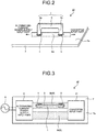
- FIG. 2 is a partially enlarged perspective view of the power conversion device 50 according to the first embodiment.
- FIG. 3 is a partially enlarged plan view of the power conversion device 50 according to the first embodiment.
- FIG. 4 is a partially enlarged front view of the power conversion device 50 according to the first embodiment.
- FIG. 5 is a partially enlarged side view of the power conversion device 50 according to the first embodiment. In FIGS. 2 to 5 , a portion between the alternating-current power-supply input part 9 and the converter input part 21 is illustrated in an enlarged manner.
- a busbar 1 is mounted on the printed wiring board 7.
- the busbar 1 is arranged to overlap the conductive pattern 6 in plan view, as illustrated in FIG. 3 .
- the busbar 1 has a first leg portion 2a and a second leg portion 2b that are respectively inserted into through holes 4 and 5 formed in the conductive pattern 6 of the printed wiring board 7 and are fixed to the printed wiring board 7 by soldering.
- the busbar 1 also has a main body portion 3 connecting the first leg portion 2a and the second leg portion 2b to each other.
- the first leg portion 2a and the second leg portion 2b are in contact with the conductive pattern 6, thereby serving as connecting portions that electrically connect the busbar 1 to the conductive pattern 6.
- Three or more connecting portions that are in contact with the conductive pattern 6 can be provided for one busbar 1.
- Each of the main body portion 3, the first leg portion 2a, and the second leg portion 2b is formed to have a shape of a rectangular or quadrangular plate.
- the first leg portion 2a and the second leg portion 2b are connected to each other by the main body portion 3, so that the busbar 1 is in the form of a U-shaped plate as a whole, as illustrated in FIG. 4 .
- the busbar 1 is mounted to form a space between the main body portion 3 and the printed wiring board 7. Further, the busbar 1 is arranged in such a manner that a plane direction thereof is perpendicular to a plane direction of the printed wiring board 7.
- Each of the main body portion 3, the first leg portion 2a, and the second leg portion 2b is configured in such a manner that a height dimension is sufficiently larger than a thickness dimension.
- the busbar 1 is connected to the conductive pattern 6 between the alternating-current power-supply input part 9 and the converter input part 21. Further, the busbar 1 is arranged to be parallel to the conductive pattern 6.
- the conductive pattern 6 can be formed on a component surface 7a of the printed wiring board 7, on which the converter circuit part 20 and the like are mounted, or on a soldering surface 7b that is a back surface of the component surface 7a, or on both the component surface 7a and the soldering surface 7b.
- a soldering surface 7b that is a back surface of the component surface 7a, or on both the component surface 7a and the soldering surface 7b.
- the conductive pattern 6 (6a, 6b, 6c, and 6d) is formed on both the component surface 7a and the soldering surface 7b is illustrated in the first embodiment.
- the busbar 1 can be arranged on the conductive pattern 6 on either one of a positive side and a negative side of an alternating-current voltage, or on the conductive pattern 6 on both the positive side and the negative side.
- the busbar 1 can be arranged on the conductive pattern 6 formed on the component surface 7a or the conductive pattern 6 formed on the soldering surface 7b. That is, although the busbar 1 is arranged on the positive-side conductive pattern 6a of the conductive pattern 6, which is formed on the component surface 7a, in the present embodiment, the negative-side conductive pattern 6b formed on the component surface 7a, the positive-side conductive pattern 6c formed on the soldering surface 7b, and the negative-side conductive pattern 6d formed on the soldering surface 7b can respectively be the object on which the busbar 1 is arranged.
- the busbar 1 is arranged to overlap the conductive pattern 6 between the alternating-current power-supply input part 9 and the converter input part 21 in the first embodiment, the busbar 1 can be arranged to overlap another conductive pattern 6. That is, the busbar 1 can be arranged to overlap the conductive pattern 6 between the converter circuit part 20 and the inverter circuit part 30, the conductive pattern 6 between the converter input part 21 and the converter output part 22, the conductive pattern 6 between the inverter input part 31 and the inverter output part 32, or the conductive pattern 6 between the inverter output part 32 and the alternating-current power-supply output part 40.
- the busbar 1 is connected to the conductive pattern 6 between the alternating-current power-supply input part 9 and the converter input part 21 through which a large current flows. Therefore, the current flowing through the conductive pattern 6 can be split in such a manner that a portion thereof flows to the side of the busbar 1. Accordingly, the current flowing through the conductive pattern 6 can be reduced, and heat dissipation from the busbar 1 can be expected. Therefore, it is possible to suppress a temperature increase in the conductive pattern 6. Further, because heat dissipation from the conductive pattern 6 can be also expected, it is possible to use a busbar 1 that is smaller than in a case where a current is made to flow through the busbar 1 only. Furthermore, because a portion of the current is split and flows to the busbar 1, the conductive pattern 6 can be made finer. Therefore, downsizing of the printed wiring board 7, that is, downsizing of the power conversion device 50 can be achieved.
- the busbar 1 is configured in such a manner that a height dimension is sufficiently larger than a thickness dimension, a mounting area of the printed wiring board 7 can be increased. Further, also in a case of increasing the size of the busbar 1 in order to improve cooling performance, it suffices that the size of the busbar 1 is increased in a height direction. Therefore, it is possible to change the size of the busbar 1 without increasing the mounting area of the printed wiring board 7.
- a thickness dimension of the busbar 1 is smaller than a width dimension of the conductive pattern 6 with which the busbar 1 is in contact. Because the busbar 1 is arranged in such a manner that the thickness dimension thereof is smaller than the width dimension of the conductive pattern 6, the busbar 1 does not protrude from a region on the conductive pattern 6, and it is possible to add the busbar 1 without increasing the mounting area of the printed wiring board 7. Furthermore, also in a case where the printed wiring board 7 is used in common by a plurality of models, it is possible to choose a specification in which the busbar 1 is mounted or a specification in which the busbar 1 is not mounted without influencing the mounting area of the printed wiring board 7 by arranging the busbar 1 in the manner described above.
- busbar 1 is arranged to overlap the conductive pattern 6 arranged in the converter input part 21. Therefore, also in a case where the converter circuit part 20 is modularized and the density of a portion around its input terminal is made high, it is possible to establish connection by using a fine conductive pattern 6.
- FIG. 6 is a partially enlarged front view of a power conversion device 51 according to a second embodiment of the present invention.
- FIG. 7 is a partially enlarged side view of the power conversion device 51 according to the second embodiment.
- Constituent elements identical to those of the first embodiment are denoted by like reference signs and redundant explanations thereof will be omitted.
- the power conversion device 51 is configured in such a manner that a height dimension of the busbar 1 is higher than heights of electronic components 11 and 12 arranged on a surface of the printed wiring board 7, on which the busbar 1 is mounted.
- a distance between the main body portion 3 of the busbar 1 and the printed wiring board 7 can be higher or lower than the height dimensions of the electronic components 11 and 12.
- a cooling capacity of a busbar can be improved by setting the height dimension of the busbar 1 to be larger than the height dimension of at least a closest electronic component to the busbar 1, of the electronic components 11 and 12.
Landscapes
- Engineering & Computer Science (AREA)
- Microelectronics & Electronic Packaging (AREA)
- Power Engineering (AREA)
- Manufacturing & Machinery (AREA)
- Inverter Devices (AREA)
Abstract
Description
- The present invention relates to a power conversion device in which a converter circuit part and an inverter circuit part are provided on a printed wiring board.
-
Patent Literature 1 discloses a configuration of a power conversion device in which a busbar extending in a thickness direction of a printed wiring board is provided on the printed wiring board as a wiring member, in place of a conductive pattern, as measures against heat generation that occurs when a current is made to flow in the printed wiring board. By providing the busbar as a wiring member, a current-carrying capacity is increased as compared with a case of providing a conductive pattern, so that a temperature increase when a current is made to flow is suppressed. - Patent Literature 1: Japanese Patent Application Laid-open No.
2014-236564 - However, the conventional technique described above has a problem that the busbar has to be made larger in order to increase the current-carrying capacity because a current flows through the busbar only, and cost is inevitably increased.
- Further, in a case of using a common printed wiring board in a plurality of models that are different from one another in current-carrying capacity, it is necessary to provide a busbar even in a model of which a current-carrying capacity is small, because the busbar is used as a wiring member. Therefore, cost is inevitably increased because of mounting of an unnecessary component.
- The present invention has been achieved in view of the above problems, and an object of the present invention is to provide a power conversion device that can suppress cost by employing a configuration corresponding to a required current-carrying capacity.
- In order to solve the above-mentioned problems and achieve the object, the present invention provides a power conversion device including: a printed wiring board on which an alternating-current power-supply input part to which alternating-current power is input, a converter circuit part to convert alternating-current power input to the alternating-current power-supply input part to direct-current power, an inverter circuit part to convert direct-current power converted by the converter circuit part to alternating-current power, an alternating-current power-supply output part to output alternating-current power converted by the inverter circuit part, and a conductive pattern to electrically connect the alternating-current power-supply input part, the converter circuit part, the inverter circuit part, and the alternating-current power-supply output part to one another are provided; and a busbar that has a plate-like shape with a plane direction thereof perpendicular to a plane direction of the printed wiring board, is arranged to overlap the conductive pattern in plan view, and includes two or more connecting portions that are in contact with the conductive pattern.
- The power conversion device according to the present invention has an effect where it is possible to suppress cost by employing a configuration corresponding to a required current-carrying capacity.
-
-
FIG. 1 is a diagram illustrating a schematic configuration of a power conversion device according to a first embodiment of the present invention. -
FIG. 2 is a partially enlarged perspective view of the power conversion device according to the first embodiment. -
FIG. 3 is a partially enlarged plan view of the power conversion device according to the first embodiment. -
FIG. 4 is a partially enlarged front view of the power conversion device according to the first embodiment. -
FIG. 5 is a partially enlarged side view of the power conversion device according to the first embodiment. -
FIG. 6 is a partially enlarged front view of a power conversion device according to a second embodiment of the present invention. -
FIG. 7 is a partially enlarged side view of the power conversion device according to the second embodiment. - A power conversion device according to embodiments of the present invention will be described in detail below with reference to the accompanying drawings. The present invention is not limited to the embodiments.
-
FIG. 1 is a diagram illustrating a schematic configuration of a power conversion device according to a first embodiment of the present invention. Apower conversion device 50 is constituted by an alternating-current power-supply input part 9, aconverter circuit part 20, aninverter circuit part 30, and an alternating-current power-supply output part 40 that are mounted on a printedwiring board 7. Aconductive pattern 6 formed on the printedwiring board 7 electrically connects the alternating-current power-supply input part 9 and theconverter circuit part 20 to each other, theconverter circuit part 20 and theinverter circuit part 30 to each other, and theinverter circuit part 30 and the alternating-current power-supply output part 40 to each other. - The
power conversion device 50 converts alternating-current power supplied from an alternating-current power supply 8 to direct-current power, converts again the direct-current power to alternating-current power with an arbitrary frequency and an arbitrary voltage, and supplies the resultant alternating-current power to a dynamic-power part 13. The dynamic-power part 13 is an electric motor, for example. - Respective power conversion are performed by cooperation of the alternating-current power-
supply input part 9, theconverter circuit part 20, theinverter circuit part 30, and the alternating-current power-supply output part 40 that are mounted on the printedwiring board 7 with one another. - That is, in the alternating-current power-
supply input part 9, alternating-current power supplied from the alternating-current power supply 8 is output to theconverter circuit part 20 via theconductive pattern 6. Theconverter circuit part 20 performs three-phase full-wave rectification on the alternating-current power by a diode bridge, thereby converting the alternating-current power to a direct-current voltage. Theconverter circuit part 20 has aconverter input part 21 and aconverter output part 22. Theconverter input part 21 and theconverter output part 22 are electrically connected to each other by theconductive pattern 6 formed on the printedwiring board 7. The alternating-current power transmitted from the alternating-current power-supply input part 9 via theconductive pattern 6 is input to theconverter input part 21 and is converted to direct-current power in theconverter circuit part 20. The resultant direct-current power is output from theconverter output part 22 to theinverter circuit part 30 via theconductive pattern 6. - The
inverter circuit part 30 converts direct-current power to alternating-current power by a switching operation of a switching element. Theinverter circuit part 30 has aninverter input part 31 and aninverter output part 32. Theinverter input part 31 and theinverter output part 32 are electrically connected to each other by theconductive pattern 6 formed on the printedwiring board 7. The direct-current power output from theconverter output part 22 is input to theinverter input part 31 and is converted to alternating-current power with an arbitrary frequency and an arbitrary voltage in theinverter circuit part 30. The resultant alternating-current power is output from theinverter output part 32 to the alternating-current power-supply output part 40 via theconductive pattern 6. - In the alternating-current power-
supply output part 40, the alternating-current power output from theinverter output part 32 is output to the dynamic-power part 13. The dynamic-power part 13 converts the alternating-current power output from the alternating-current power-supply output part 40 to dynamic power. - The
conductive pattern 6 formed on the printedwiring board 7 in thepower conversion device 50 configured in the above manner is described.FIG. 2 is a partially enlarged perspective view of thepower conversion device 50 according to the first embodiment.FIG. 3 is a partially enlarged plan view of thepower conversion device 50 according to the first embodiment.FIG. 4 is a partially enlarged front view of thepower conversion device 50 according to the first embodiment.FIG. 5 is a partially enlarged side view of thepower conversion device 50 according to the first embodiment. InFIGS. 2 to 5 , a portion between the alternating-current power-supply input part 9 and theconverter input part 21 is illustrated in an enlarged manner. - A
busbar 1 is mounted on the printedwiring board 7. Thebusbar 1 is arranged to overlap theconductive pattern 6 in plan view, as illustrated inFIG. 3 . Thebusbar 1 has afirst leg portion 2a and asecond leg portion 2b that are respectively inserted into throughholes conductive pattern 6 of the printedwiring board 7 and are fixed to the printedwiring board 7 by soldering. Thebusbar 1 also has amain body portion 3 connecting thefirst leg portion 2a and thesecond leg portion 2b to each other. Thefirst leg portion 2a and thesecond leg portion 2b are in contact with theconductive pattern 6, thereby serving as connecting portions that electrically connect thebusbar 1 to theconductive pattern 6. Three or more connecting portions that are in contact with theconductive pattern 6 can be provided for onebusbar 1. - Each of the
main body portion 3, thefirst leg portion 2a, and thesecond leg portion 2b is formed to have a shape of a rectangular or quadrangular plate. Thefirst leg portion 2a and thesecond leg portion 2b are connected to each other by themain body portion 3, so that thebusbar 1 is in the form of a U-shaped plate as a whole, as illustrated inFIG. 4 . Thebusbar 1 is mounted to form a space between themain body portion 3 and the printedwiring board 7. Further, thebusbar 1 is arranged in such a manner that a plane direction thereof is perpendicular to a plane direction of the printedwiring board 7. - Each of the
main body portion 3, thefirst leg portion 2a, and thesecond leg portion 2b is configured in such a manner that a height dimension is sufficiently larger than a thickness dimension. InFIGS. 2 to 5 , thebusbar 1 is connected to theconductive pattern 6 between the alternating-current power-supply input part 9 and theconverter input part 21. Further, thebusbar 1 is arranged to be parallel to theconductive pattern 6. - The
conductive pattern 6 can be formed on acomponent surface 7a of the printedwiring board 7, on which theconverter circuit part 20 and the like are mounted, or on asoldering surface 7b that is a back surface of thecomponent surface 7a, or on both thecomponent surface 7a and thesoldering surface 7b. An example in which the conductive pattern 6 (6a, 6b, 6c, and 6d) is formed on both thecomponent surface 7a and thesoldering surface 7b is illustrated in the first embodiment. Further, thebusbar 1 can be arranged on theconductive pattern 6 on either one of a positive side and a negative side of an alternating-current voltage, or on theconductive pattern 6 on both the positive side and the negative side. Furthermore, thebusbar 1 can be arranged on theconductive pattern 6 formed on thecomponent surface 7a or theconductive pattern 6 formed on thesoldering surface 7b. That is, although thebusbar 1 is arranged on the positive-sideconductive pattern 6a of theconductive pattern 6, which is formed on thecomponent surface 7a, in the present embodiment, the negative-sideconductive pattern 6b formed on thecomponent surface 7a, the positive-sideconductive pattern 6c formed on thesoldering surface 7b, and the negative-sideconductive pattern 6d formed on thesoldering surface 7b can respectively be the object on which thebusbar 1 is arranged. - Although the
busbar 1 is arranged to overlap theconductive pattern 6 between the alternating-current power-supply input part 9 and theconverter input part 21 in the first embodiment, thebusbar 1 can be arranged to overlap anotherconductive pattern 6. That is, thebusbar 1 can be arranged to overlap theconductive pattern 6 between theconverter circuit part 20 and theinverter circuit part 30, theconductive pattern 6 between theconverter input part 21 and theconverter output part 22, theconductive pattern 6 between theinverter input part 31 and theinverter output part 32, or theconductive pattern 6 between theinverter output part 32 and the alternating-current power-supply output part 40. - As described above, in the
power conversion device 50 according to the first embodiment, thebusbar 1 is connected to theconductive pattern 6 between the alternating-current power-supply input part 9 and theconverter input part 21 through which a large current flows. Therefore, the current flowing through theconductive pattern 6 can be split in such a manner that a portion thereof flows to the side of thebusbar 1. Accordingly, the current flowing through theconductive pattern 6 can be reduced, and heat dissipation from thebusbar 1 can be expected. Therefore, it is possible to suppress a temperature increase in theconductive pattern 6. Further, because heat dissipation from theconductive pattern 6 can be also expected, it is possible to use abusbar 1 that is smaller than in a case where a current is made to flow through thebusbar 1 only. Furthermore, because a portion of the current is split and flows to thebusbar 1, theconductive pattern 6 can be made finer. Therefore, downsizing of the printedwiring board 7, that is, downsizing of thepower conversion device 50 can be achieved. - In addition, because the
busbar 1 is configured in such a manner that a height dimension is sufficiently larger than a thickness dimension, a mounting area of the printedwiring board 7 can be increased. Further, also in a case of increasing the size of thebusbar 1 in order to improve cooling performance, it suffices that the size of thebusbar 1 is increased in a height direction. Therefore, it is possible to change the size of thebusbar 1 without increasing the mounting area of the printedwiring board 7. - Further, in a case where a large current-carrying capacity is required in the
power conversion device 50, such a large current-carrying capacity can be achieved by increasing the size of thebusbar 1. In a case where only a small current-carrying capacity is required in thepower conversion device 50, it is possible to employ a configuration in which thebusbar 1 is not provided, because power is supplied from the alternating-current power-supply input part 9 to theconverter input part 21 via theconductive pattern 6. Furthermore, because power is supplied from the alternating-current power-supply input part 9 to theconverter input part 21 via theconductive pattern 6 as described above, downsizing of thebusbar 1 can be achieved as compared with a case where power is supplied by thebusbar 1 only. As described above, in thepower conversion device 50 according to the first embodiment, it is possible to suppress cost by employing a configuration corresponding to a required current-carrying capacity. - As illustrated in
FIG. 5 , a thickness dimension of thebusbar 1 is smaller than a width dimension of theconductive pattern 6 with which thebusbar 1 is in contact. Because thebusbar 1 is arranged in such a manner that the thickness dimension thereof is smaller than the width dimension of theconductive pattern 6, thebusbar 1 does not protrude from a region on theconductive pattern 6, and it is possible to add thebusbar 1 without increasing the mounting area of the printedwiring board 7. Furthermore, also in a case where the printedwiring board 7 is used in common by a plurality of models, it is possible to choose a specification in which thebusbar 1 is mounted or a specification in which thebusbar 1 is not mounted without influencing the mounting area of the printedwiring board 7 by arranging thebusbar 1 in the manner described above. - Further, the
busbar 1 is arranged to overlap theconductive pattern 6 arranged in theconverter input part 21. Therefore, also in a case where theconverter circuit part 20 is modularized and the density of a portion around its input terminal is made high, it is possible to establish connection by using a fineconductive pattern 6. -
FIG. 6 is a partially enlarged front view of apower conversion device 51 according to a second embodiment of the present invention.FIG. 7 is a partially enlarged side view of thepower conversion device 51 according to the second embodiment. Constituent elements identical to those of the first embodiment are denoted by like reference signs and redundant explanations thereof will be omitted. - As illustrated in
FIGS. 6 and 7 , thepower conversion device 51 according to the second embodiment is configured in such a manner that a height dimension of thebusbar 1 is higher than heights ofelectronic components wiring board 7, on which thebusbar 1 is mounted. A distance between themain body portion 3 of thebusbar 1 and the printedwiring board 7 can be higher or lower than the height dimensions of theelectronic components - As described above, by setting the height dimension of the
busbar 1 to be larger than the height dimensions of theelectronic components busbar 1 becomes less likely to be interfered. In a case where the printedwiring board 7 is forcibly cooled by causing a cooling air from a blower to blow thereto, the cooling air can hit thebusbar 1 more easily. Therefore, a cooling capacity can be improved. Further, also in a case where forcible cooling by using a blower is not performed, it is possible to reduce an influence of heat radiated from thebusbar 1 on theelectronic components busbar 1. Therefore, it is possible to suppress a temperature increase of the electronic components. A cooling capacity of a busbar can be improved by setting the height dimension of thebusbar 1 to be larger than the height dimension of at least a closest electronic component to thebusbar 1, of theelectronic components - The configurations described in the above embodiments are only examples of the content of the present invention. The configurations can be combined with other well-known techniques, and a part of each configuration can be omitted or modified without departing from the scope of the present invention.
- 1 busbar, 2a first leg portion, 2b second leg portion, 3 main body portion, 4, 5 through hole, 6 conductive pattern, 7 printed wiring board, 7a component surface, 7b soldering surface, 8 alternating-current power supply, 9 alternating-current power-supply input part, 11, 12 electronic component, 13 dynamic-power part, 20 converter circuit part, 21 converter input part, 22 converter output part, 30 inverter circuit part, 31 inverter input part, 32 inverter output part, 40 alternating-current power-supply output part, 50, 51 power conversion device.
Claims (5)
- A power conversion device comprising:a printed wiring board on which an alternating-current power-supply input part to which alternating-current power is input, a converter circuit part to convert alternating-current power input to the alternating-current power-supply input part to direct-current power, an inverter circuit part to convert direct-current power converted by the converter circuit part to alternating-current power, an alternating-current power-supply output part to output alternating-current power converted by the inverter circuit part, and a conductive pattern to electrically connect the alternating-current power-supply input part, the converter circuit part, the inverter circuit part, and the alternating-current power-supply output part to one another are provided; anda busbar that has a plate-like shape with a plane direction thereof perpendicular to a plane direction of the printed wiring board, is arranged to overlap the conductive pattern in plan view, and includes two or more connecting portions that are in contact with the conductive pattern.
- The power conversion device according to claim 1, wherein a thickness of the printed wiring board is smaller than a width of the conductive pattern with which the two connecting portions are in contact.
- The power conversion device according to claim 1, further comprising electronic components provided on a surface of the printed wiring board, on which the busbar is arranged, wherein
a height of the busbar is higher than a height of an electronic component that is closest to the busbar. - The power conversion device according to any one of claims 1 to 3, wherein the connecting portions of the busbar are in contact with a conductive pattern that connects the converter circuit part and the inverter circuit part to each other.
- The power conversion device according to any one of claims 1 to 3, wherein the connecting portions of the busbar are in contact with a conductive pattern that connects the inverter circuit part and the alternating-current power-supply output part to each other.
Applications Claiming Priority (1)
| Application Number | Priority Date | Filing Date | Title |
|---|---|---|---|
| PCT/JP2016/051730 WO2017126086A1 (en) | 2016-01-21 | 2016-01-21 | Power conversion device |
Publications (3)
| Publication Number | Publication Date |
|---|---|
| EP3407478A1 true EP3407478A1 (en) | 2018-11-28 |
| EP3407478A4 EP3407478A4 (en) | 2019-01-30 |
| EP3407478B1 EP3407478B1 (en) | 2020-04-15 |
Family
ID=59361732
Family Applications (1)
| Application Number | Title | Priority Date | Filing Date |
|---|---|---|---|
| EP16886327.2A Active EP3407478B1 (en) | 2016-01-21 | 2016-01-21 | Power conversion device |
Country Status (5)
| Country | Link |
|---|---|
| US (1) | US10432106B2 (en) |
| EP (1) | EP3407478B1 (en) |
| JP (1) | JP6662911B2 (en) |
| CN (1) | CN108604866B (en) |
| WO (1) | WO2017126086A1 (en) |
Cited By (1)
| Publication number | Priority date | Publication date | Assignee | Title |
|---|---|---|---|---|
| CN116614005A (en) * | 2023-05-17 | 2023-08-18 | 深圳迈格瑞能技术有限公司 | Layout structure of full-bridge circuit |
Families Citing this family (2)
| Publication number | Priority date | Publication date | Assignee | Title |
|---|---|---|---|---|
| JP2022049051A (en) * | 2020-09-16 | 2022-03-29 | ファナック株式会社 | Connection structure |
| JP2023041377A (en) * | 2021-09-13 | 2023-03-24 | 株式会社富士通ゼネラル | Power substrate and outdoor machine of air conditioner using the same |
Family Cites Families (24)
| Publication number | Priority date | Publication date | Assignee | Title |
|---|---|---|---|---|
| JPS6016110A (en) * | 1983-07-05 | 1985-01-26 | 住友電気工業株式会社 | Device for mutually connecting wire ring harness |
| JPS63122296A (en) * | 1986-11-12 | 1988-05-26 | フアナツク株式会社 | Control unit |
| JPH0639474Y2 (en) * | 1987-03-24 | 1994-10-12 | 松下電器産業株式会社 | Large current circuit device |
| JP3734157B2 (en) * | 2001-10-11 | 2006-01-11 | 株式会社デンソー | Inverter device |
| JP2004335887A (en) | 2003-05-09 | 2004-11-25 | Canon Inc | Printed wiring board and apparatus using the board |
| US7154761B1 (en) * | 2004-02-13 | 2006-12-26 | Cisco Technology, Inc. | Techniques for distributing current in a backplane assembly and methods for making the same |
| JP2005341641A (en) * | 2004-05-24 | 2005-12-08 | Daito Electron Co Ltd | Bus bar |
| US20050265059A1 (en) * | 2004-05-27 | 2005-12-01 | Tracy John G | Multi-use power conversion modules |
| US20060050494A1 (en) * | 2004-09-03 | 2006-03-09 | Cotek Electronic Ind. Co. Ltd. | DC-AC power inverter |
| JP4470688B2 (en) * | 2004-10-29 | 2010-06-02 | 株式会社日立製作所 | Mounting structure of bus bar structure, power supply device, power supply system, electronic circuit board, electronic device |
| JP4730116B2 (en) * | 2005-04-11 | 2011-07-20 | 株式会社デンソー | Discharge lamp lighting device |
| JP2008078364A (en) * | 2006-09-21 | 2008-04-03 | Sumitomo Wiring Syst Ltd | Formation method of circuit material and circuit material formed by method |
| JP5319979B2 (en) * | 2008-07-28 | 2013-10-16 | 株式会社ケーヒン | Terminal with busbar |
| JP2010104135A (en) * | 2008-10-23 | 2010-05-06 | Hitachi Ltd | Power conversion apparatus and electrical machine system for mobile |
| JP4929299B2 (en) * | 2009-02-17 | 2012-05-09 | 株式会社日立製作所 | Power converter |
| JP2011036017A (en) * | 2009-07-31 | 2011-02-17 | Daikin Industries Ltd | Power conversion apparatus |
| JP2012110152A (en) * | 2010-11-18 | 2012-06-07 | Nabtesco Corp | Converter |
| EP2787627B1 (en) * | 2011-11-28 | 2022-12-07 | Nissan Motor Co., Ltd. | Power conversion device |
| US20150365037A1 (en) * | 2013-03-07 | 2015-12-17 | Mitsubishi Electric Corporation | Alternating current motor drive system |
| JP2014236564A (en) | 2013-05-31 | 2014-12-15 | 株式会社ケーヒン | Bus bar |
| JP2015142472A (en) * | 2014-01-30 | 2015-08-03 | 住友重機械工業株式会社 | Busbar structure, power conversion device and work machine |
| JP6198941B2 (en) * | 2014-05-07 | 2017-09-20 | 株式会社日立製作所 | Power converter |
| JP6137411B2 (en) * | 2014-07-01 | 2017-05-31 | 富士電機株式会社 | Power converter |
| JP5778840B1 (en) * | 2014-09-25 | 2015-09-16 | 株式会社日立製作所 | Power conversion unit and power conversion device |
-
2016
- 2016-01-21 US US15/771,115 patent/US10432106B2/en active Active
- 2016-01-21 WO PCT/JP2016/051730 patent/WO2017126086A1/en not_active Ceased
- 2016-01-21 CN CN201680076302.4A patent/CN108604866B/en active Active
- 2016-01-21 JP JP2017562236A patent/JP6662911B2/en active Active
- 2016-01-21 EP EP16886327.2A patent/EP3407478B1/en active Active
Cited By (2)
| Publication number | Priority date | Publication date | Assignee | Title |
|---|---|---|---|---|
| CN116614005A (en) * | 2023-05-17 | 2023-08-18 | 深圳迈格瑞能技术有限公司 | Layout structure of full-bridge circuit |
| CN116614005B (en) * | 2023-05-17 | 2024-06-21 | 深圳迈格瑞能技术有限公司 | Layout structure of full-bridge circuit |
Also Published As
| Publication number | Publication date |
|---|---|
| EP3407478A4 (en) | 2019-01-30 |
| WO2017126086A1 (en) | 2017-07-27 |
| CN108604866B (en) | 2020-06-12 |
| US10432106B2 (en) | 2019-10-01 |
| JPWO2017126086A1 (en) | 2018-05-10 |
| CN108604866A (en) | 2018-09-28 |
| JP6662911B2 (en) | 2020-03-11 |
| EP3407478B1 (en) | 2020-04-15 |
| US20180316274A1 (en) | 2018-11-01 |
Similar Documents
| Publication | Publication Date | Title |
|---|---|---|
| US12232288B2 (en) | Assembly structure | |
| JP5344013B2 (en) | Power converter | |
| US12262515B2 (en) | Inverter of compact design | |
| JP6648859B2 (en) | Power converter | |
| US11626718B2 (en) | Motor drive apparatus including bus bar | |
| US9935558B2 (en) | DC-DC converter apparatus including single drive circuit board arranged at predetermined interval from metal base | |
| JP2016115623A (en) | Module-terminal block connection structure and connection method | |
| EP3407478B1 (en) | Power conversion device | |
| US9788449B2 (en) | Power conversion apparatus | |
| CN205069920U (en) | Busbar is used in installation of metal printed circuit board in vehicle | |
| JP2019088137A (en) | Power conversion equipment | |
| WO2022264864A1 (en) | Bus bar heat dissipation structure and inverter device | |
| CN206370781U (en) | power conversion device | |
| CN209250499U (en) | High power inverter | |
| JP2013074022A (en) | Semiconductor control device | |
| JP2020022235A (en) | Power conversion device and bus bar | |
| CN214125849U (en) | PCB heat abstractor, PCB heat dissipation assembly and dc-to-ac converter | |
| CN223613610U (en) | Power board layout structure, transformer mounting structure and inverter | |
| JP7134305B1 (en) | power converter | |
| EP4444052A1 (en) | Dual-inverter assembly | |
| JP6870458B2 (en) | Power converter | |
| JP2015171309A (en) | Circuit structure and electrical junction box | |
| JPH07111390A (en) | Power supply |
Legal Events
| Date | Code | Title | Description |
|---|---|---|---|
| STAA | Information on the status of an ep patent application or granted ep patent |
Free format text: STATUS: THE INTERNATIONAL PUBLICATION HAS BEEN MADE |
|
| PUAI | Public reference made under article 153(3) epc to a published international application that has entered the european phase |
Free format text: ORIGINAL CODE: 0009012 |
|
| STAA | Information on the status of an ep patent application or granted ep patent |
Free format text: STATUS: REQUEST FOR EXAMINATION WAS MADE |
|
| 17P | Request for examination filed |
Effective date: 20180716 |
|
| AK | Designated contracting states |
Kind code of ref document: A1 Designated state(s): AL AT BE BG CH CY CZ DE DK EE ES FI FR GB GR HR HU IE IS IT LI LT LU LV MC MK MT NL NO PL PT RO RS SE SI SK SM TR |
|
| AX | Request for extension of the european patent |
Extension state: BA ME |
|
| A4 | Supplementary search report drawn up and despatched |
Effective date: 20190107 |
|
| RIC1 | Information provided on ipc code assigned before grant |
Ipc: H02M 5/458 20060101AFI20181221BHEP Ipc: H05K 3/22 20060101ALN20181221BHEP Ipc: H05K 1/02 20060101ALN20181221BHEP Ipc: H02M 7/00 20060101ALI20181221BHEP Ipc: H05K 1/18 20060101ALN20181221BHEP |
|
| DAV | Request for validation of the european patent (deleted) | ||
| DAX | Request for extension of the european patent (deleted) | ||
| STAA | Information on the status of an ep patent application or granted ep patent |
Free format text: STATUS: EXAMINATION IS IN PROGRESS |
|
| 17Q | First examination report despatched |
Effective date: 20190626 |
|
| RIC1 | Information provided on ipc code assigned before grant |
Ipc: H05K 1/02 20060101ALN20191009BHEP Ipc: H05K 3/22 20060101ALN20191009BHEP Ipc: H05K 1/18 20060101ALN20191009BHEP Ipc: H02M 7/00 20060101ALI20191009BHEP Ipc: H02M 5/458 20060101AFI20191009BHEP |
|
| GRAP | Despatch of communication of intention to grant a patent |
Free format text: ORIGINAL CODE: EPIDOSNIGR1 |
|
| STAA | Information on the status of an ep patent application or granted ep patent |
Free format text: STATUS: GRANT OF PATENT IS INTENDED |
|
| INTG | Intention to grant announced |
Effective date: 20191128 |
|
| GRAS | Grant fee paid |
Free format text: ORIGINAL CODE: EPIDOSNIGR3 |
|
| GRAA | (expected) grant |
Free format text: ORIGINAL CODE: 0009210 |
|
| STAA | Information on the status of an ep patent application or granted ep patent |
Free format text: STATUS: THE PATENT HAS BEEN GRANTED |
|
| AK | Designated contracting states |
Kind code of ref document: B1 Designated state(s): AL AT BE BG CH CY CZ DE DK EE ES FI FR GB GR HR HU IE IS IT LI LT LU LV MC MK MT NL NO PL PT RO RS SE SI SK SM TR |
|
| REG | Reference to a national code |
Ref country code: CH Ref legal event code: EP |
|
| REG | Reference to a national code |
Ref country code: DE Ref legal event code: R096 Ref document number: 602016034302 Country of ref document: DE |
|
| REG | Reference to a national code |
Ref country code: IE Ref legal event code: FG4D |
|
| REG | Reference to a national code |
Ref country code: AT Ref legal event code: REF Ref document number: 1258466 Country of ref document: AT Kind code of ref document: T Effective date: 20200515 |
|
| REG | Reference to a national code |
Ref country code: NL Ref legal event code: MP Effective date: 20200415 |
|
| REG | Reference to a national code |
Ref country code: LT Ref legal event code: MG4D |
|
| PG25 | Lapsed in a contracting state [announced via postgrant information from national office to epo] |
Ref country code: PT Free format text: LAPSE BECAUSE OF FAILURE TO SUBMIT A TRANSLATION OF THE DESCRIPTION OR TO PAY THE FEE WITHIN THE PRESCRIBED TIME-LIMIT Effective date: 20200817 Ref country code: LT Free format text: LAPSE BECAUSE OF FAILURE TO SUBMIT A TRANSLATION OF THE DESCRIPTION OR TO PAY THE FEE WITHIN THE PRESCRIBED TIME-LIMIT Effective date: 20200415 Ref country code: NL Free format text: LAPSE BECAUSE OF FAILURE TO SUBMIT A TRANSLATION OF THE DESCRIPTION OR TO PAY THE FEE WITHIN THE PRESCRIBED TIME-LIMIT Effective date: 20200415 Ref country code: FI Free format text: LAPSE BECAUSE OF FAILURE TO SUBMIT A TRANSLATION OF THE DESCRIPTION OR TO PAY THE FEE WITHIN THE PRESCRIBED TIME-LIMIT Effective date: 20200415 Ref country code: SE Free format text: LAPSE BECAUSE OF FAILURE TO SUBMIT A TRANSLATION OF THE DESCRIPTION OR TO PAY THE FEE WITHIN THE PRESCRIBED TIME-LIMIT Effective date: 20200415 Ref country code: IS Free format text: LAPSE BECAUSE OF FAILURE TO SUBMIT A TRANSLATION OF THE DESCRIPTION OR TO PAY THE FEE WITHIN THE PRESCRIBED TIME-LIMIT Effective date: 20200815 Ref country code: GR Free format text: LAPSE BECAUSE OF FAILURE TO SUBMIT A TRANSLATION OF THE DESCRIPTION OR TO PAY THE FEE WITHIN THE PRESCRIBED TIME-LIMIT Effective date: 20200716 Ref country code: NO Free format text: LAPSE BECAUSE OF FAILURE TO SUBMIT A TRANSLATION OF THE DESCRIPTION OR TO PAY THE FEE WITHIN THE PRESCRIBED TIME-LIMIT Effective date: 20200715 |
|
| REG | Reference to a national code |
Ref country code: AT Ref legal event code: MK05 Ref document number: 1258466 Country of ref document: AT Kind code of ref document: T Effective date: 20200415 |
|
| PG25 | Lapsed in a contracting state [announced via postgrant information from national office to epo] |
Ref country code: LV Free format text: LAPSE BECAUSE OF FAILURE TO SUBMIT A TRANSLATION OF THE DESCRIPTION OR TO PAY THE FEE WITHIN THE PRESCRIBED TIME-LIMIT Effective date: 20200415 Ref country code: BG Free format text: LAPSE BECAUSE OF FAILURE TO SUBMIT A TRANSLATION OF THE DESCRIPTION OR TO PAY THE FEE WITHIN THE PRESCRIBED TIME-LIMIT Effective date: 20200715 Ref country code: HR Free format text: LAPSE BECAUSE OF FAILURE TO SUBMIT A TRANSLATION OF THE DESCRIPTION OR TO PAY THE FEE WITHIN THE PRESCRIBED TIME-LIMIT Effective date: 20200415 Ref country code: RS Free format text: LAPSE BECAUSE OF FAILURE TO SUBMIT A TRANSLATION OF THE DESCRIPTION OR TO PAY THE FEE WITHIN THE PRESCRIBED TIME-LIMIT Effective date: 20200415 |
|
| PG25 | Lapsed in a contracting state [announced via postgrant information from national office to epo] |
Ref country code: AL Free format text: LAPSE BECAUSE OF FAILURE TO SUBMIT A TRANSLATION OF THE DESCRIPTION OR TO PAY THE FEE WITHIN THE PRESCRIBED TIME-LIMIT Effective date: 20200415 |
|
| REG | Reference to a national code |
Ref country code: DE Ref legal event code: R097 Ref document number: 602016034302 Country of ref document: DE |
|
| PG25 | Lapsed in a contracting state [announced via postgrant information from national office to epo] |
Ref country code: CZ Free format text: LAPSE BECAUSE OF FAILURE TO SUBMIT A TRANSLATION OF THE DESCRIPTION OR TO PAY THE FEE WITHIN THE PRESCRIBED TIME-LIMIT Effective date: 20200415 Ref country code: ES Free format text: LAPSE BECAUSE OF FAILURE TO SUBMIT A TRANSLATION OF THE DESCRIPTION OR TO PAY THE FEE WITHIN THE PRESCRIBED TIME-LIMIT Effective date: 20200415 Ref country code: RO Free format text: LAPSE BECAUSE OF FAILURE TO SUBMIT A TRANSLATION OF THE DESCRIPTION OR TO PAY THE FEE WITHIN THE PRESCRIBED TIME-LIMIT Effective date: 20200415 Ref country code: EE Free format text: LAPSE BECAUSE OF FAILURE TO SUBMIT A TRANSLATION OF THE DESCRIPTION OR TO PAY THE FEE WITHIN THE PRESCRIBED TIME-LIMIT Effective date: 20200415 Ref country code: SM Free format text: LAPSE BECAUSE OF FAILURE TO SUBMIT A TRANSLATION OF THE DESCRIPTION OR TO PAY THE FEE WITHIN THE PRESCRIBED TIME-LIMIT Effective date: 20200415 Ref country code: DK Free format text: LAPSE BECAUSE OF FAILURE TO SUBMIT A TRANSLATION OF THE DESCRIPTION OR TO PAY THE FEE WITHIN THE PRESCRIBED TIME-LIMIT Effective date: 20200415 Ref country code: IT Free format text: LAPSE BECAUSE OF FAILURE TO SUBMIT A TRANSLATION OF THE DESCRIPTION OR TO PAY THE FEE WITHIN THE PRESCRIBED TIME-LIMIT Effective date: 20200415 Ref country code: AT Free format text: LAPSE BECAUSE OF FAILURE TO SUBMIT A TRANSLATION OF THE DESCRIPTION OR TO PAY THE FEE WITHIN THE PRESCRIBED TIME-LIMIT Effective date: 20200415 |
|
| PLBE | No opposition filed within time limit |
Free format text: ORIGINAL CODE: 0009261 |
|
| STAA | Information on the status of an ep patent application or granted ep patent |
Free format text: STATUS: NO OPPOSITION FILED WITHIN TIME LIMIT |
|
| PG25 | Lapsed in a contracting state [announced via postgrant information from national office to epo] |
Ref country code: SK Free format text: LAPSE BECAUSE OF FAILURE TO SUBMIT A TRANSLATION OF THE DESCRIPTION OR TO PAY THE FEE WITHIN THE PRESCRIBED TIME-LIMIT Effective date: 20200415 Ref country code: PL Free format text: LAPSE BECAUSE OF FAILURE TO SUBMIT A TRANSLATION OF THE DESCRIPTION OR TO PAY THE FEE WITHIN THE PRESCRIBED TIME-LIMIT Effective date: 20200415 |
|
| 26N | No opposition filed |
Effective date: 20210118 |
|
| PG25 | Lapsed in a contracting state [announced via postgrant information from national office to epo] |
Ref country code: SI Free format text: LAPSE BECAUSE OF FAILURE TO SUBMIT A TRANSLATION OF THE DESCRIPTION OR TO PAY THE FEE WITHIN THE PRESCRIBED TIME-LIMIT Effective date: 20200415 |
|
| PG25 | Lapsed in a contracting state [announced via postgrant information from national office to epo] |
Ref country code: MC Free format text: LAPSE BECAUSE OF FAILURE TO SUBMIT A TRANSLATION OF THE DESCRIPTION OR TO PAY THE FEE WITHIN THE PRESCRIBED TIME-LIMIT Effective date: 20200415 |
|
| REG | Reference to a national code |
Ref country code: CH Ref legal event code: PL |
|
| GBPC | Gb: european patent ceased through non-payment of renewal fee |
Effective date: 20210121 |
|
| PG25 | Lapsed in a contracting state [announced via postgrant information from national office to epo] |
Ref country code: LU Free format text: LAPSE BECAUSE OF NON-PAYMENT OF DUE FEES Effective date: 20210121 |
|
| REG | Reference to a national code |
Ref country code: BE Ref legal event code: MM Effective date: 20210131 |
|
| PG25 | Lapsed in a contracting state [announced via postgrant information from national office to epo] |
Ref country code: FR Free format text: LAPSE BECAUSE OF NON-PAYMENT OF DUE FEES Effective date: 20210131 |
|
| PG25 | Lapsed in a contracting state [announced via postgrant information from national office to epo] |
Ref country code: CH Free format text: LAPSE BECAUSE OF NON-PAYMENT OF DUE FEES Effective date: 20210131 Ref country code: LI Free format text: LAPSE BECAUSE OF NON-PAYMENT OF DUE FEES Effective date: 20210131 Ref country code: GB Free format text: LAPSE BECAUSE OF NON-PAYMENT OF DUE FEES Effective date: 20210121 |
|
| PG25 | Lapsed in a contracting state [announced via postgrant information from national office to epo] |
Ref country code: IE Free format text: LAPSE BECAUSE OF NON-PAYMENT OF DUE FEES Effective date: 20210121 |
|
| PG25 | Lapsed in a contracting state [announced via postgrant information from national office to epo] |
Ref country code: BE Free format text: LAPSE BECAUSE OF NON-PAYMENT OF DUE FEES Effective date: 20210131 |
|
| P01 | Opt-out of the competence of the unified patent court (upc) registered |
Effective date: 20230512 |
|
| PG25 | Lapsed in a contracting state [announced via postgrant information from national office to epo] |
Ref country code: CY Free format text: LAPSE BECAUSE OF FAILURE TO SUBMIT A TRANSLATION OF THE DESCRIPTION OR TO PAY THE FEE WITHIN THE PRESCRIBED TIME-LIMIT Effective date: 20200415 |
|
| PG25 | Lapsed in a contracting state [announced via postgrant information from national office to epo] |
Ref country code: HU Free format text: LAPSE BECAUSE OF FAILURE TO SUBMIT A TRANSLATION OF THE DESCRIPTION OR TO PAY THE FEE WITHIN THE PRESCRIBED TIME-LIMIT; INVALID AB INITIO Effective date: 20160121 |
|
| PG25 | Lapsed in a contracting state [announced via postgrant information from national office to epo] |
Ref country code: MK Free format text: LAPSE BECAUSE OF FAILURE TO SUBMIT A TRANSLATION OF THE DESCRIPTION OR TO PAY THE FEE WITHIN THE PRESCRIBED TIME-LIMIT Effective date: 20200415 |
|
| PG25 | Lapsed in a contracting state [announced via postgrant information from national office to epo] |
Ref country code: TR Free format text: LAPSE BECAUSE OF FAILURE TO SUBMIT A TRANSLATION OF THE DESCRIPTION OR TO PAY THE FEE WITHIN THE PRESCRIBED TIME-LIMIT Effective date: 20200415 |
|
| PG25 | Lapsed in a contracting state [announced via postgrant information from national office to epo] |
Ref country code: MT Free format text: LAPSE BECAUSE OF FAILURE TO SUBMIT A TRANSLATION OF THE DESCRIPTION OR TO PAY THE FEE WITHIN THE PRESCRIBED TIME-LIMIT Effective date: 20200415 |
|
| PGFP | Annual fee paid to national office [announced via postgrant information from national office to epo] |
Ref country code: DE Payment date: 20241203 Year of fee payment: 10 |