EP3407374A1 - Power generation device for generating electricity using heat - Google Patents
Power generation device for generating electricity using heat Download PDFInfo
- Publication number
- EP3407374A1 EP3407374A1 EP18158146.3A EP18158146A EP3407374A1 EP 3407374 A1 EP3407374 A1 EP 3407374A1 EP 18158146 A EP18158146 A EP 18158146A EP 3407374 A1 EP3407374 A1 EP 3407374A1
- Authority
- EP
- European Patent Office
- Prior art keywords
- power generation
- configuration
- conductive layer
- crystal
- generation element
- Prior art date
- Legal status (The legal status is an assumption and is not a legal conclusion. Google has not performed a legal analysis and makes no representation as to the accuracy of the status listed.)
- Granted
Links
Images



Classifications
-
- H—ELECTRICITY
- H01—ELECTRIC ELEMENTS
- H01J—ELECTRIC DISCHARGE TUBES OR DISCHARGE LAMPS
- H01J45/00—Discharge tubes functioning as thermionic generators
-
- H—ELECTRICITY
- H02—GENERATION; CONVERSION OR DISTRIBUTION OF ELECTRIC POWER
- H02N—ELECTRIC MACHINES NOT OTHERWISE PROVIDED FOR
- H02N11/00—Generators or motors not provided for elsewhere; Alleged perpetua mobilia obtained by electric or magnetic means
- H02N11/002—Generators
-
- H—ELECTRICITY
- H02—GENERATION; CONVERSION OR DISTRIBUTION OF ELECTRIC POWER
- H02N—ELECTRIC MACHINES NOT OTHERWISE PROVIDED FOR
- H02N3/00—Generators in which thermal or kinetic energy is converted into electrical energy by ionisation of a fluid and removal of the charge therefrom
-
- H—ELECTRICITY
- H10—SEMICONDUCTOR DEVICES; ELECTRIC SOLID-STATE DEVICES NOT OTHERWISE PROVIDED FOR
- H10N—ELECTRIC SOLID-STATE DEVICES NOT OTHERWISE PROVIDED FOR
- H10N10/00—Thermoelectric devices comprising a junction of dissimilar materials, i.e. devices exhibiting Seebeck or Peltier effects
- H10N10/80—Constructional details
-
- H—ELECTRICITY
- H10—SEMICONDUCTOR DEVICES; ELECTRIC SOLID-STATE DEVICES NOT OTHERWISE PROVIDED FOR
- H10N—ELECTRIC SOLID-STATE DEVICES NOT OTHERWISE PROVIDED FOR
- H10N70/00—Solid-state devices having no potential barriers, and specially adapted for rectifying, amplifying, oscillating or switching
-
- H—ELECTRICITY
- H10—SEMICONDUCTOR DEVICES; ELECTRIC SOLID-STATE DEVICES NOT OTHERWISE PROVIDED FOR
- H10N—ELECTRIC SOLID-STATE DEVICES NOT OTHERWISE PROVIDED FOR
- H10N15/00—Thermoelectric devices without a junction of dissimilar materials; Thermomagnetic devices, e.g. using the Nernst-Ettingshausen effect
Definitions
- Embodiments described herein relate generally to a power generation element, a power generation module, a power generation device, and a power generation system.
- a power generation element including an emitter electrode and a collector electrode, wherein heat from a heat source is applied to the emitter electrode, and the collector electrode captures thermal electrons from the emitter electrode. It is desirable to increase the efficiency of the power generation element.
- a power generation element includes a first conductive layer, a second conductive layer, a first member, and a second member.
- the first member includes a first crystal and is provided between the first conductive layer and the second conductive layer.
- the first crystal has a wurtzite structure.
- the second member is separated from the first member and is provided between the first member and the second conductive layer.
- a ⁇ 000-1> direction of the first crystal has a component from the first member toward the second member.
- a power generation element includes a first conductive layer, a second conductive layer, a first member, and a second member.
- the first member is provided between the first conductive layer and the second conductive layer.
- the second member is separated from the first member and is provided between the first member and the second conductive layer.
- An orientation from negative to positive of a polarization of the first member is from the first member toward the second member.
- a power generation module includes one of a plurality of the power generation elements described above.
- a power generation device includes a plurality of the power generation modules described above.
- a power generation system includes the power generation device described above and a drive device.
- the drive device causes the power generation device to follow a movement of the sun.
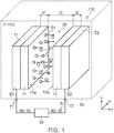
- FIG. 1 is a schematic perspective view illustrating a power generation element according to a first embodiment.
- the power generation element 110 includes a first conductive layer E1, a second conductive layer E2, a first member 11, and a second member 12.
- the first member 11 is provided between the first conductive layer E1 and the second conductive layer E2.
- the first member 11 includes, for example, a first crystal having a wurtzite structure.
- the second member 12 is provided between the first member 11 and the second conductive layer E2.
- the second member 12 is separated from the first member 11.
- the second member 12 includes a second crystal having a wurtzite structure.
- the first crystal and the second crystal are, for example, AlN.
- a gap 20 is provided between the first member 11 and the second member 12.
- the gap 20 is in a reduced-pressure state.
- a container 70 is provided.
- the first member 11 and the second member 12 are provided in the interior of the container 70.
- the interior of the container 70 is caused to be in a reduced-pressure state.
- the gap 20 is in a reduced-pressure state.
- the first member 11 is electrically connected to the first conductive layer E1.
- the second member 12 is electrically connected to the second conductive layer E2.
- a first terminal 71 and a second terminal 72 are provided.
- the first terminal 71 is electrically connected to the first conductive layer E1.
- the second terminal 72 is electrically connected to the second conductive layer E2.
- a load 30 is electrically connectable between the first terminal 71 and the second terminal 72.
- the temperature of the first conductive layer E1 (and the first member 11) is taken as a first temperature T1.
- the temperature of the second conductive layer E2 (and the second member 12) is taken as a second temperature T2.
- the temperature (the first temperature T1) of the first member 11 is caused to be higher than the temperature (the second temperature T2) of the second member 12.
- the first conductive layer E1 (and the first member 11) are connected to a heat source, etc. Thereby, the first temperature T1 becomes higher than the second temperature T2.
- electrons 51 are emitted from the first member 11.
- the electrons 51 are, for example, thermal electrons.
- the electrons 51 travel toward the second member 12.
- the electrons 51 reach the second member 12.
- the electrons 51 that reach the second member 12 flow into the load 30 via the second conductive layer E2 and the second terminal 72.
- the flow of the electrons 51 corresponds to a current.
- the temperature difference between the first conductive layer E1 (and the first member 11) and the second conductive layer E2 (and the second member 12) can be converted into a current.
- the first conductive layer E1 (and the first member 11) is, for example, an emitter.
- the second conductive layer E2 (and the second member 12) is, for example, a collector.
- a direction from the first member 11 toward the second member 12 is taken as a Z-axis direction.
- the Z-axis direction corresponds to the direction from the first conductive layer E1 toward the second conductive layer E2.
- One direction perpendicular to the Z-axis direction is taken as an X-axis direction.
- a direction perpendicular to the Z-axis direction and the X-axis direction is taken as a Y-axis direction.
- first member 11 and the second member 12 have film configurations spreading along the X-Y plane.
- the configurations of the first member 11 and the second member 12 are arbitrary.
- At least one of the first crystal or the second crystal includes, for example, nitrogen and at least one selected from the group consisting of B, Al, In, and Ga. At least one of the first crystal or the second crystal may include at least one selected from the group consisting of ZnO and ZnMgO.
- a thickness t1 of the first member 11 is, for example, not less than 100 nm and not more than 1000 nm. In the case where the first member 11 is insulative, the thickness t1 of the first member 11 is, for example, 5 nm or less. In the case where the first member 11 is insulative, it is favorable for the thickness t1 to be not less than 1 nm and not more than 2 nm.
- a thickness t2 of the second member 12 is, for example, not less than 100 nm and not more than 1000 nm. In the case where the second member 12 is insulative, the thickness t2 of the second member 12 is, for example, 5 nm or less. In the case where the second member 12 is insulative, it is favorable for the thickness t2 to be not less than 1 nm and not more than 2 nm.
- the thickness t1 and the thickness t2 are lengths along the Z-axis direction.
- a distance t3 between the first member 11 and the second member 12 is not less than 0.1 ⁇ m and not more than 50 ⁇ m. It is more favorable for the distance t3 to be 10 ⁇ m or less.
- the distance t3 is the length along the Z-axis direction. The distance t3 corresponds to the distance of the gap 20.
- the ⁇ 000-1> direction of the first crystal of the first member 11 has a component from the first member 11 toward the second member 12.
- the first member 11 has a first surface 11a.
- the first surface 11a opposes the second member 12.
- the first surface 11a is, for example, the (000-1) plane.
- the first surface 11a may be a semi-polar plane.
- the ⁇ 000-1> direction of the second crystal of the second member 12 has a component from the second member 12 toward the first member 11.
- the second member 12 has a second surface 12a.
- the second surface 12a opposes the first member 11.
- the second surface 12a is, for example, the (000-1) plane.
- the second surface 12a may be a semi-polar plane.
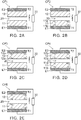
- FIG. 2A to FIG. 2E are schematic cross-sectional views illustrating the power generation element.
- first conductive layer E1 and the second conductive layer E2 are Mo layers.
- the first member 11 and the second member 12 are AlN.
- the thickness of the AlN is 2000 nm.
- the distance of the gap 20 (the length along the Z-axis direction, i.e., the distance t3) is 1 ⁇ m.
- the first member 11 and the second member 12 do not have polarizations (spontaneous polarizations).
- the first configuration CF1 corresponds to the case where the first member 11 and the second member 12 are amorphous.
- the first member 11 has a polarization.
- the first member 11 has the first surface 11a on the second member 12 side, and a surface 11b on the first conductive layer E1 side.
- the polarization is positive (+ ⁇ ) at the first surface 11a.
- the polarization is negative (- ⁇ ) at the surface 11b.
- the first surface 11a is the -c plane (the (000-1) plane).
- the surface 11b is the +c plane (the (0001) plane).
- the second member 12 does not have a polarization.
- the second member 12 has a polarization.
- the second member 12 has the second surface 12a on the first member 11 side, and a surface 12b on the second conductive layer E2 side.
- the polarization is positive (+ ⁇ ) at the second surface 12a.
- the polarization is negative (- ⁇ ) at the surface 12b.
- the second surface 12a is the -c plane (the (000-1) plane).
- the surface 12b is the +c plane (the (0001) plane).
- the first member 11 does not have a polarization.
- the first member 11 and the second member 12 have polarizations.
- the orientations of the polarizations are mutually-reversed.
- the polarization is positive (+ ⁇ ) at the first surface 11a.
- the first surface 11a is the -c plane (the (000-1) plane).
- the polarization is positive (+ ⁇ ) at the second surface 12a.
- the second surface 12a is the -c plane (the (000-1) plane).
- the first member 11 and the second member 12 have polarizations.
- the orientations of the polarizations of the fifth configuration CF5 are the reverse of the orientations of the polarizations of the fourth configuration CF4.
- FIG. 3A to FIG. 3D are schematic views illustrating characteristics of the power generation element.
- FIGS. 1 to CF5. are energy band diagrams of the first to fifth configurations CF1 to CF5.
- the first temperature T1 and the second temperature T2 are 300 K (Kelvin).
- the horizontal axis is a position pZ ( ⁇ m) along the Z-axis direction.
- the vertical axis is an energy Eg (electron volt (eV)).
- FIG. 3A A Fermi level FL1 of the first configuration CF1, a conduction band level CB1 of the first configuration CF1, a Fermi level FL2 of the second configuration CF2, and a conduction band level CB2 of the second configuration CF2 are shown in FIG. 3A . It can be seen from FIG. 3A that compared to the first configuration CF1, the energy Eg at the surface of the first member 11 (the surface between the first member 11 and the gap 20) is different for the second configuration CF2.
- FIG. 3B a Fermi level FL3 of the third configuration CF3 and a conduction band level CB3 of the third configuration CF3 are shown in addition to the Fermi level FL1 of the first configuration CF1 and the conduction band level CB1 of the first configuration CF1. It can be seen from FIG. 3B that the energy Eg at the surface of the second member 12 (the surface between the second member 12 and the gap 20) of the third configuration CF3 is different from the energy Eg of the first configuration CF1.
- a Fermi level FL4 of the fourth configuration CF4 and a conduction band level CB4 of the fourth configuration CF4 are shown in addition to the Fermi level FL1 of the first configuration CF1 and the conduction band level CB1 of the first configuration CF1. It can be seen from FIG. 3C that the energy Eg of the fourth configuration CF4 is different from the energy Eg of the first configuration CF1 at the surface of the first member 11 and the surface of the second member 12.
- a Fermi level FL5 of the fifth configuration CF5 and a conduction band level CB5 of the fifth configuration CF5 are shown in addition to the Fermi level FL1 of the first configuration CF1 and the conduction band level CB1 of the first configuration CF1 in FIG. 3D . It can be seen from FIG. 3D that compared to the first to fourth configurations CF1 to CF4, the energy Eg is markedly large for the fifth configuration CF5.
- the energy Eg of the conduction band level is markedly high in the case where the surfaces of the first member 11 and the second member 12 are the +c plane (the (0001) plane). Therefore, it is considered that the thermal electrons (the electrons 51) are not emitted easily for the fifth configuration CF5.
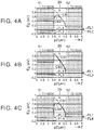
- FIG. 4A to FIG. 4C are schematic views illustrating the characteristics of the power generation element.
- FIGS. 1 to CF4 are energy band diagrams of the first to fourth configurations CF1 to CF4.
- the first temperature T1 is 800 K; and the second temperature T2 is 300 K.
- a simulation of the characteristics of the fifth configuration CF5 was attempted; but the calculated values did not converge; and the characteristics of the fifth configuration CF5 were not obtained.
- the horizontal axis is the position pZ.
- the vertical axis is the energy Eg.
- the conduction band level CB2 of the second configuration CF2 is lower than the conduction band level CB1 of the first configuration CF1 at the surface of the first member 11 (the surface between the first member 11 and the gap 20).
- the conduction band level CB3 of the third configuration CF3 is lower than the conduction band level CB1 of the first configuration CF1 at the surface of the second member 12 (the second member 12 and the gap 20).
- the conduction band level CB4 of the fourth configuration CF4 is lower than the conduction band level CB1 of the first configuration CF1 at the surface of the first member 11 and the surface of the second member 12.
- the energy Eg at the surface is low due to at least one of the first member 11 or the second member 12 having the polarization of the polarity recited above.
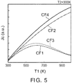
- FIG. 5 is a graph illustrating a characteristic of the power generation element.
- FIG. 5 shows simulation results of the power generation characteristics of the first to fourth configurations CF1 to CF4.
- the horizontal axis of FIG. 5 is the first temperature T1 (Kelvin (K)).
- the vertical axis is a current density Jc (arbitrary units).
- the second temperature T2 is 300 K.
- the current density Jc of the third configuration CF3 is higher than the current density Jc of the first configuration CF1.
- the current density Jc of the second configuration CF2 is higher than the current density Jc of the third configuration CF3.
- the current density Jc of the fourth configuration CF4 is higher than the current density Jc of the second configuration CF2.
- a high current density Jc is obtained by at least one of the first member 11 or the second member 12 having the polarization of the polarity recited above.
- a particularly high current density Jc (the second configuration CF2 and the fourth configuration CF4) is obtained by the first member 11 of which the temperature is caused to be relatively high having the polarization of the polarity recited above.
- a particularly high current density Jc (the fourth configuration CF4) is obtained by both the first member 11 and the second member 12 having the polarizations of the polarities recited above.
- the high current density Jc corresponds to a high efficiency.
- a high efficiency is obtained by at least one of the first member 11 or the second member 12 having the polarization of the polarity recited above.
- Such a high current density Jc is caused by the characteristics of the conduction bands described in reference to FIG. 4A to FIG. 4C .
- the characteristics of the conduction bands are the characteristics of the barrier height at the surfaces of the first member 11 and the second member 12. It is considered that the barrier height has a relationship with the electron affinity.
- the electron affinities of the materials of the first member 11 and the second member 12 themselves have a relationship with the power generation efficiency.
- An example of the power generation efficiency of the first configuration CF1 and the fourth configuration CF4 when changing the electron affinity will now be described.
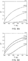
- FIG. 6A and FIG. 6B are graphs illustrating characteristics of the power generation element.
- FIG. 6A corresponds to a characteristic of the first configuration CF1.
- FIG. 6B corresponds to a characteristic of the fourth configuration CF4.
- the horizontal axis is the first temperature T1.
- the vertical axis is a power generation efficiency Ef (arbitrary units).
- the second temperature T2 is 300 K.
- electron affinities ⁇ of the first member 11 and the second member 12 are modified to 0.3, 0.45, or 0.6.
- the power generation efficiency Ef of the fourth configuration CF4 is higher than the power generation efficiency Ef of the first configuration CF1 for the same first temperature T1 when the electron affinity ⁇ is 0.3, 0.45, or 0.6.
- the improvement effect of the power generation efficiency Ef due to the fourth configuration CF4 is large when the electron affinity ⁇ is high.
- At least one of the first member 11 or the second member 12 includes a crystal having a wurtzite structure. At least one of the first member 11 or the second member 12 includes, for example, a nitride semiconductor. Or, at least one of the first member 11 or the second member 12 includes at least one selected from the group consisting of ZnO and ZnMgO.
- At least one of the first member 11 or the second member 12 may include an insulative material.
- at least one of the first member 11 or the second member 12 may include at least one selected from the group consisting of BaTiO 3 , PbTiO 3 , Pb(Zr x , Ti 1- x )O 3 , KNbO 3 , LiNbO 3 , LiTaO 3 , Na x WO 3 , Zn 2 O 3 , Ba 2 NaNb 5 O 5 , Pb 2 KNb 5 O 15 , and Li 2 B 4 O 7 .
- Pb(Zr x , Ti 1- x )O 3 is PZT (lead zirconate titanate).
- the orientation from negative to positive of the polarization of the first member 11 is from the first member 11 toward the second member 12.
- the orientation from negative to positive of the polarization of the second member 12 is from the second member 12 toward the first member 11. Even in such a case, a high efficiency is obtained.
- the thicknesses of the first member 11 and the second member 12 are thin. Thereby, the current flows easily.
- the thickness t1 of the first member 11 (the length along the direction from the first member 11 toward the second member 12) is 5 nm or less.
- the thickness t1 may be not less than 1 nm and not more than 2 nm.
- the thickness t2 (the length along the direction from the second member 12 toward the first member 11) of the second member 12 is 5 nm or less.
- the thickness t2 may be not less than 1 nm and not more than 2 nm.
- At least one of the first member 11 or the second member 12 may have an island configuration or a mesh configuration.
- At least one of the first member 11 or the second member 12 may include a semiconductor crystal.
- the semiconductor crystal includes, for example, nitrogen and at least one selected from the group consisting of B, Al, In, and Ga.
- at least one of the first member 11 or the second member 12 includes at least one selected from the group consisting of ZnO and ZnMgO.
- a second embodiment is related to a method for manufacturing a power generation element.
- the power generation element 110 according to the first embodiment can be manufactured by the manufacturing method.
- FIG. 7A to FIG. 7E are schematic cross-sectional views illustrating the method for manufacturing the power generation element according to the second embodiment.
- a first film 11F is formed on a base body 50s.
- the first film 11F is used to form at least one of the first member 11 or the second member 12.
- a Si substrate, an Al 2 O 3 substrate, a SiC substrate, or the like is used as the base body 50s.
- crystal growth of the first film 11F is performed by metal organic chemical vapor deposition (MOCVD), etc.
- MOCVD metal organic chemical vapor deposition
- the first film 11F may be formed by crystal growth using molecular beam epitaxy (MBE), etc.
- the first film 11F is, for example, a crystal of a nitride semiconductor.
- the surface (the upper surface) of the first film 11F is the +c plane.
- the lower surface (the surface on the base body 50s side) of the first film 11F is the -c plane.
- a conductive layer E0 is formed on the first film 11F.
- the conductive layer E0 is at least one of the first conductive layer E1 or the second conductive layer E2.
- the conductive layer E0 includes, for example, at least one selected from the group consisting of Mo and W.
- the conductive layer E0 is formed by vapor deposition.
- the conductive layer E0 may be Mo or W having a wafer configuration. In such a case, for example, the conductive layer E0 is bonded to the first film 11F.
- the base body 50s is removed as shown in FIG. 7C .
- the surface of the first film 11F is the -c plane.
- Such a structure body including the conductive layer E0 and the first film 11F is multiply prepared.
- the conductive layer E0 is used as the first conductive layer E1; and the first film 11F is used as the first member 11.
- the conductive layer E0 is used as the second conductive layer E2; and the first film 11F is used as the second member 12.
- the first member 11 and the second member 12 are assembled so that the first member 11 and the second member 12 oppose each other.
- the power generation element 110 according to the embodiment is made.
- FIG. 8A and FIG. 8B are schematic cross-sectional views showing a power generation module and a power generation device according to the embodiment.
- the power generation module 210 includes the power generation element 110 according to the first embodiment.
- multiple power generation elements 110 are arranged on a substrate 120.
- the power generation device 310 includes the power generation module 210 recited above. Multiple power generation modules 210 may be provided. In the example, the multiple power generation modules 210 are arranged on a substrate 220.
- FIG. 9A and FIG. 9B are schematic views showing a power generation device and a power generation system according to the embodiment.
- the power generation device 310 according to the embodiment i.e., the power generation element 110 or the power generation module 210 according to the first embodiment
- the power generation device 310 is applicable to solar thermal power generation.
- the light from the sun 61 is reflected by a heliostat 62 and is incident on the power generation device 310 (the power generation element 110 or the power generation module 210).
- the light causes the first temperature T1 of the first member 11 and the first conductive layer E1 to increase.
- the first temperature T1 becomes higher than the second temperature T2. Heat is changed into current.
- the current is transmitted by a power line 65, etc.
- the light from the sun 61 is concentrated by a concentrating mirror 63 and is incident on the power generation device 310 (the power generation element 110 or the power generation module 210).
- the heat due to the light is changed into current.
- the current is transmitted by the power line 65, etc.
- the power generation system 410 includes the power generation device 310.
- multiple power generation devices 310 are provided.
- the power generation system 410 includes the power generation devices 310 and a drive device 66.
- the drive device 66 causes the power generation devices 310 to follow the movement of the sun 61. By following the movement of the sun 61, efficient power generation can be performed.
- Highly efficient power generation can be performed by using the power generation element 110 according to the embodiment.
- the embodiments may include the following configurations (technological proposals).
- a power generation element comprising:
- the power generation element according to Configuration 1 or 2 wherein the second member includes a second crystal having a wurtzite structure, and the ⁇ 000-1> direction of the second crystal has a component from the second member toward the first member.
- the power generation element according to any one of Configurations 1 to 6, wherein the first crystal includes nitrogen and at least one selected from the group consisting of B, Al, In, and Ga.
- the power generation element according to any one of Configurations 1 to 6, wherein the first crystal includes at least one selected from the group consisting of ZnO and ZnMgO.
- a power generation element comprising:
- the second member includes at least one selected from the group consisting of BaTiO 3 , PbTiO 3 , Pb(Zr x , Ti 1-x )O 3 , KNbO 3 , LiNbO 3 , LiTaO 3 , Na x WO 3 , Zn 2 O 3 , Ba 2 NaNb 5 O 5 , Pb 2 KNb 5 O 15 , and Li 2 B 4 O 7 .
- the power generation element according to Configuration 10 wherein the second member includes a second crystal, and the second crystal includes nitrogen and at least one selected from the group consisting of B, Al, In, and Ga.
- the power generation element according to any one of Configurations 9 to 14, wherein the first member includes at least one selected from the group consisting of BaTiO 3 , PbTiO 3 , Pb(Zr x , Ti 1- x )O 3 , KNbO 3 , LiNbO 3 , LiTaO 3 , Na x WO 3 , Zn 2 O 3 , Ba 2 NaNb 5 O 5 , Pb 2 KNb 5 O 15 , and Li 2 B 4 O 7 .
- the power generation element according to Configuration 9 wherein the first member includes a first crystal, and the first crystal includes nitrogen and at least one selected from the group consisting of B, Al, In, and Ga.
- the power generation element according to any one of Configurations 1 to 18, further comprising:
- a power generation module comprising a plurality of the power generation elements according to any one of Configurations 1 to 20.
- a power generation device comprising a plurality of the power generation modules according to Configuration 21.
- a power generation system comprising:
- a power generation element, a power generation module, a power generation device, and a power generation system can be provided in which the efficiency can be increased.
- nitride semiconductor includes all compositions of semiconductors of the chemical formula B x In y Al,Ga 1- x - y - z N (0 ⁇ x ⁇ 1, 0 ⁇ y ⁇ 1, 0 ⁇ z ⁇ 1, and x + y + z ⁇ 1) for which the composition ratios x, y, and z are changed within the ranges respectively.
- N nitrogen
Landscapes
- Chemical & Material Sciences (AREA)
- Chemical Kinetics & Catalysis (AREA)
- Battery Electrode And Active Subsutance (AREA)
- Photovoltaic Devices (AREA)
Abstract
Description
- Embodiments described herein relate generally to a power generation element, a power generation module, a power generation device, and a power generation system.
- For example, there is a power generation element including an emitter electrode and a collector electrode, wherein heat from a heat source is applied to the emitter electrode, and the collector electrode captures thermal electrons from the emitter electrode. It is desirable to increase the efficiency of the power generation element.
-
-
FIG. 1 is a schematic perspective view illustrating a power generation element according to a first embodiment; -
FIG. 2A to FIG. 2E are schematic cross-sectional views illustrating the power generation element; -
FIG. 3A to FIG. 3D are schematic views illustrating characteristics of the power generation element; -
FIG. 4A to FIG. 4C are schematic views illustrating the characteristics of the power generation element; -
FIG. 5 is a graph illustrating a characteristic of the power generation element; -
FIG. 6A and FIG. 6B are graphs illustrating characteristics of the power generation element; -
FIG. 7A to FIG. 7E are schematic cross-sectional views illustrating the method for manufacturing the power generation element according to the second embodiment; -
FIG. 8A and FIG. 8B are schematic cross-sectional views showing a power generation module and a power generation device according to the embodiment; and -
FIG. 9A and FIG. 9B are schematic views showing a power generation device and a power generation system according to the embodiment. - According to one embodiment, a power generation element includes a first conductive layer, a second conductive layer, a first member, and a second member. The first member includes a first crystal and is provided between the first conductive layer and the second conductive layer. The first crystal has a wurtzite structure. The second member is separated from the first member and is provided between the first member and the second conductive layer. A <000-1> direction of the first crystal has a component from the first member toward the second member.
- According to another embodiment, a power generation element includes a first conductive layer, a second conductive layer, a first member, and a second member. The first member is provided between the first conductive layer and the second conductive layer. The second member is separated from the first member and is provided between the first member and the second conductive layer. An orientation from negative to positive of a polarization of the first member is from the first member toward the second member.
- According to another embodiment, a power generation module includes one of a plurality of the power generation elements described above.
- According to another embodiment, a power generation device includes a plurality of the power generation modules described above.
- According to another embodiment, a power generation system includes the power generation device described above and a drive device. The drive device causes the power generation device to follow a movement of the sun.
- Various embodiments will be described hereinafter with reference to the accompanying drawings.
- The drawings are schematic and conceptual; and the relationships between the thickness and width of portions, the proportions of sizes among portions, etc., are not necessarily the same as the actual values thereof. Further, the dimensions and proportions may be illustrated differently among drawings, even for identical portions.
- In the specification and drawings, components similar to those described or illustrated in a drawing thereinabove are marked with like reference numerals, and a detailed description is omitted as appropriate.
-
FIG. 1 is a schematic perspective view illustrating a power generation element according to a first embodiment. - As shown in
FIG. 1 , thepower generation element 110 according to the first embodiment includes a first conductive layer E1, a second conductive layer E2, afirst member 11, and asecond member 12. - The
first member 11 is provided between the first conductive layer E1 and the second conductive layer E2. Thefirst member 11 includes, for example, a first crystal having a wurtzite structure. Thesecond member 12 is provided between thefirst member 11 and the second conductive layer E2. Thesecond member 12 is separated from thefirst member 11. For example, thesecond member 12 includes a second crystal having a wurtzite structure. The first crystal and the second crystal are, for example, AlN. - A
gap 20 is provided between thefirst member 11 and thesecond member 12. Thegap 20 is in a reduced-pressure state. For example, acontainer 70 is provided. For example, thefirst member 11 and thesecond member 12 are provided in the interior of thecontainer 70. The interior of thecontainer 70 is caused to be in a reduced-pressure state. Thereby, thegap 20 is in a reduced-pressure state. - For example, the
first member 11 is electrically connected to the first conductive layer E1. Thesecond member 12 is electrically connected to the second conductive layer E2. Afirst terminal 71 and asecond terminal 72 are provided. Thefirst terminal 71 is electrically connected to the first conductive layer E1. Thesecond terminal 72 is electrically connected to the second conductive layer E2. Aload 30 is electrically connectable between thefirst terminal 71 and thesecond terminal 72. - For example, the temperature of the first conductive layer E1 (and the first member 11) is taken as a first temperature T1. The temperature of the second conductive layer E2 (and the second member 12) is taken as a second temperature T2. For example, the temperature (the first temperature T1) of the
first member 11 is caused to be higher than the temperature (the second temperature T2) of thesecond member 12. For example, the first conductive layer E1 (and the first member 11) are connected to a heat source, etc. Thereby, the first temperature T1 becomes higher than the second temperature T2. Thereby,electrons 51 are emitted from thefirst member 11. Theelectrons 51 are, for example, thermal electrons. Theelectrons 51 travel toward thesecond member 12. Theelectrons 51 reach thesecond member 12. - The
electrons 51 that reach thesecond member 12 flow into theload 30 via the second conductive layer E2 and thesecond terminal 72. The flow of theelectrons 51 corresponds to a current. - Thus, in the
power generation element 110, the temperature difference between the first conductive layer E1 (and the first member 11) and the second conductive layer E2 (and the second member 12) can be converted into a current. - The first conductive layer E1 (and the first member 11) is, for example, an emitter. The second conductive layer E2 (and the second member 12) is, for example, a collector.
- A direction from the
first member 11 toward thesecond member 12 is taken as a Z-axis direction. The Z-axis direction corresponds to the direction from the first conductive layer E1 toward the second conductive layer E2. One direction perpendicular to the Z-axis direction is taken as an X-axis direction. A direction perpendicular to the Z-axis direction and the X-axis direction is taken as a Y-axis direction. - In the example, the
first member 11 and thesecond member 12 have film configurations spreading along the X-Y plane. In the embodiment, the configurations of thefirst member 11 and thesecond member 12 are arbitrary. - At least one of the first crystal or the second crystal includes, for example, nitrogen and at least one selected from the group consisting of B, Al, In, and Ga. At least one of the first crystal or the second crystal may include at least one selected from the group consisting of ZnO and ZnMgO.
- In the case where the
first member 11 is a semiconductor, a thickness t1 of thefirst member 11 is, for example, not less than 100 nm and not more than 1000 nm. In the case where thefirst member 11 is insulative, the thickness t1 of thefirst member 11 is, for example, 5 nm or less. In the case where thefirst member 11 is insulative, it is favorable for the thickness t1 to be not less than 1 nm and not more than 2 nm. - In the case where the
second member 12 is a semiconductor, a thickness t2 of thesecond member 12 is, for example, not less than 100 nm and not more than 1000 nm. In the case where thesecond member 12 is insulative, the thickness t2 of thesecond member 12 is, for example, 5 nm or less. In the case where thesecond member 12 is insulative, it is favorable for the thickness t2 to be not less than 1 nm and not more than 2 nm. The thickness t1 and the thickness t2 are lengths along the Z-axis direction. - A distance t3 between the
first member 11 and thesecond member 12 is not less than 0.1 µm and not more than 50 µm. It is more favorable for the distance t3 to be 10 µm or less. The distance t3 is the length along the Z-axis direction. The distance t3 corresponds to the distance of thegap 20. - In the embodiment, the <000-1> direction of the first crystal of the
first member 11 has a component from thefirst member 11 toward thesecond member 12. For example, thefirst member 11 has afirst surface 11a. Thefirst surface 11a opposes thesecond member 12. Thefirst surface 11a is, for example, the (000-1) plane. Thefirst surface 11a may be a semi-polar plane. - In the embodiment, for example, the <000-1> direction of the second crystal of the
second member 12 has a component from thesecond member 12 toward thefirst member 11. For example, thesecond member 12 has asecond surface 12a. Thesecond surface 12a opposes thefirst member 11. Thesecond surface 12a is, for example, the (000-1) plane. Thesecond surface 12a may be a semi-polar plane. - It was found that a high power generation efficiency is obtained by the first member 11 (and the second member 12) having polarities such as those recited above.
- An example of simulation results of the characteristics of the power generation element will now be described.
-
FIG. 2A to FIG. 2E are schematic cross-sectional views illustrating the power generation element. - These drawings show the configuration that is used in the simulation. In the simulation, the first conductive layer E1 and the second conductive layer E2 are Mo layers. The
first member 11 and thesecond member 12 are AlN. The thickness of the AlN is 2000 nm. The distance of the gap 20 (the length along the Z-axis direction, i.e., the distance t3) is 1 µm. - In a first configuration CF1 shown in
FIG. 2A , thefirst member 11 and thesecond member 12 do not have polarizations (spontaneous polarizations). For example, the first configuration CF1 corresponds to the case where thefirst member 11 and thesecond member 12 are amorphous. - In a second configuration CF2 shown in
FIG. 2B , thefirst member 11 has a polarization. Thefirst member 11 has thefirst surface 11a on thesecond member 12 side, and asurface 11b on the first conductive layer E1 side. The polarization is positive (+σ) at thefirst surface 11a. The polarization is negative (-σ) at thesurface 11b. Thefirst surface 11a is the -c plane (the (000-1) plane). Thesurface 11b is the +c plane (the (0001) plane). In the second configuration CF2, thesecond member 12 does not have a polarization. - In a third configuration CF3 shown in
FIG. 2C , thesecond member 12 has a polarization. Thesecond member 12 has thesecond surface 12a on thefirst member 11 side, and asurface 12b on the second conductive layer E2 side. The polarization is positive (+σ) at thesecond surface 12a. The polarization is negative (-σ) at thesurface 12b. Thesecond surface 12a is the -c plane (the (000-1) plane). Thesurface 12b is the +c plane (the (0001) plane). In the third configuration CF3, thefirst member 11 does not have a polarization. - In a fourth configuration CF4 shown in
FIG. 2D , thefirst member 11 and thesecond member 12 have polarizations. The orientations of the polarizations are mutually-reversed. The polarization is positive (+σ) at thefirst surface 11a. Thefirst surface 11a is the -c plane (the (000-1) plane). The polarization is positive (+σ) at thesecond surface 12a. Thesecond surface 12a is the -c plane (the (000-1) plane). - In a fifth configuration CF5 shown in
FIG. 2E as well, thefirst member 11 and thesecond member 12 have polarizations. The orientations of the polarizations of the fifth configuration CF5 are the reverse of the orientations of the polarizations of the fourth configuration CF4. -
FIG. 3A to FIG. 3D are schematic views illustrating characteristics of the power generation element. - These figures are energy band diagrams of the first to fifth configurations CF1 to CF5. For these configurations, the first temperature T1 and the second temperature T2 are 300 K (Kelvin). In these drawings, the horizontal axis is a position pZ (µm) along the Z-axis direction. The vertical axis is an energy Eg (electron volt (eV)).
- A Fermi level FL1 of the first configuration CF1, a conduction band level CB1 of the first configuration CF1, a Fermi level FL2 of the second configuration CF2, and a conduction band level CB2 of the second configuration CF2 are shown in
FIG. 3A . It can be seen fromFIG. 3A that compared to the first configuration CF1, the energy Eg at the surface of the first member 11 (the surface between thefirst member 11 and the gap 20) is different for the second configuration CF2. - In
FIG. 3B , a Fermi level FL3 of the third configuration CF3 and a conduction band level CB3 of the third configuration CF3 are shown in addition to the Fermi level FL1 of the first configuration CF1 and the conduction band level CB1 of the first configuration CF1. It can be seen fromFIG. 3B that the energy Eg at the surface of the second member 12 (the surface between thesecond member 12 and the gap 20) of the third configuration CF3 is different from the energy Eg of the first configuration CF1. - In
FIG. 3C , a Fermi level FL4 of the fourth configuration CF4 and a conduction band level CB4 of the fourth configuration CF4 are shown in addition to the Fermi level FL1 of the first configuration CF1 and the conduction band level CB1 of the first configuration CF1. It can be seen fromFIG. 3C that the energy Eg of the fourth configuration CF4 is different from the energy Eg of the first configuration CF1 at the surface of thefirst member 11 and the surface of thesecond member 12. - A Fermi level FL5 of the fifth configuration CF5 and a conduction band level CB5 of the fifth configuration CF5 are shown in addition to the Fermi level FL1 of the first configuration CF1 and the conduction band level CB1 of the first configuration CF1 in
FIG. 3D . It can be seen fromFIG. 3D that compared to the first to fourth configurations CF1 to CF4, the energy Eg is markedly large for the fifth configuration CF5. - It can be seen from
FIG. 3A to FIG. 3C that in the case where the surface of thefirst member 11 or thesecond member 12 is the -c plane (the (000-1) plane), the energy Eg of the conduction band level is low at these surfaces. - On the other hand, as shown in
FIG. 3D , the energy Eg of the conduction band level is markedly high in the case where the surfaces of thefirst member 11 and thesecond member 12 are the +c plane (the (0001) plane). Therefore, it is considered that the thermal electrons (the electrons 51) are not emitted easily for the fifth configuration CF5. - An example of characteristics when the first temperature T1 is set to be higher than the second temperature T2 will now be described.
-
FIG. 4A to FIG. 4C are schematic views illustrating the characteristics of the power generation element. - These figures are energy band diagrams of the first to fourth configurations CF1 to CF4. For these configurations, the first temperature T1 is 800 K; and the second temperature T2 is 300 K. A simulation of the characteristics of the fifth configuration CF5 was attempted; but the calculated values did not converge; and the characteristics of the fifth configuration CF5 were not obtained. In these drawings, the horizontal axis is the position pZ. The vertical axis is the energy Eg.
- As shown in
FIG. 4A , the conduction band level CB2 of the second configuration CF2 is lower than the conduction band level CB1 of the first configuration CF1 at the surface of the first member 11 (the surface between thefirst member 11 and the gap 20). - As shown in
FIG. 4B , the conduction band level CB3 of the third configuration CF3 is lower than the conduction band level CB1 of the first configuration CF1 at the surface of the second member 12 (thesecond member 12 and the gap 20). - As shown in
FIG. 4C , the conduction band level CB4 of the fourth configuration CF4 is lower than the conduction band level CB1 of the first configuration CF1 at the surface of thefirst member 11 and the surface of thesecond member 12. - Thus, the energy Eg at the surface is low due to at least one of the
first member 11 or thesecond member 12 having the polarization of the polarity recited above. -
FIG. 5 is a graph illustrating a characteristic of the power generation element. -
FIG. 5 shows simulation results of the power generation characteristics of the first to fourth configurations CF1 to CF4. The horizontal axis ofFIG. 5 is the first temperature T1 (Kelvin (K)). The vertical axis is a current density Jc (arbitrary units). In the example, the second temperature T2 is 300 K. - As shown in
FIG. 5 , the current density Jc of the third configuration CF3 is higher than the current density Jc of the first configuration CF1. The current density Jc of the second configuration CF2 is higher than the current density Jc of the third configuration CF3. The current density Jc of the fourth configuration CF4 is higher than the current density Jc of the second configuration CF2. - Thus, a high current density Jc is obtained by at least one of the
first member 11 or thesecond member 12 having the polarization of the polarity recited above. In particular, a particularly high current density Jc (the second configuration CF2 and the fourth configuration CF4) is obtained by thefirst member 11 of which the temperature is caused to be relatively high having the polarization of the polarity recited above. For example, a particularly high current density Jc (the fourth configuration CF4) is obtained by both thefirst member 11 and thesecond member 12 having the polarizations of the polarities recited above. The high current density Jc corresponds to a high efficiency. A high efficiency is obtained by at least one of thefirst member 11 or thesecond member 12 having the polarization of the polarity recited above. - For example, it is considered that such a high current density Jc is caused by the characteristics of the conduction bands described in reference to
FIG. 4A to FIG. 4C . The characteristics of the conduction bands are the characteristics of the barrier height at the surfaces of thefirst member 11 and thesecond member 12. It is considered that the barrier height has a relationship with the electron affinity. - In the power generation element, it is considered that the electron affinities of the materials of the
first member 11 and thesecond member 12 themselves have a relationship with the power generation efficiency. An example of the power generation efficiency of the first configuration CF1 and the fourth configuration CF4 when changing the electron affinity will now be described. -
FIG. 6A and FIG. 6B are graphs illustrating characteristics of the power generation element. -
FIG. 6A corresponds to a characteristic of the first configuration CF1.FIG. 6B corresponds to a characteristic of the fourth configuration CF4. In these figures, the horizontal axis is the first temperature T1. The vertical axis is a power generation efficiency Ef (arbitrary units). In the simulation of these figures, the second temperature T2 is 300 K. In the simulation, electron affinities χ of thefirst member 11 and thesecond member 12 are modified to 0.3, 0.45, or 0.6. - As shown in
FIG. 6A and FIG. 6B , the power generation efficiency Ef of the fourth configuration CF4 is higher than the power generation efficiency Ef of the first configuration CF1 for the same first temperature T1 when the electron affinity χ is 0.3, 0.45, or 0.6. In particular, the improvement effect of the power generation efficiency Ef due to the fourth configuration CF4 is large when the electron affinity χ is high. - In the embodiment as described above, at least one of the
first member 11 or thesecond member 12 includes a crystal having a wurtzite structure. At least one of thefirst member 11 or thesecond member 12 includes, for example, a nitride semiconductor. Or, at least one of thefirst member 11 or thesecond member 12 includes at least one selected from the group consisting of ZnO and ZnMgO. - In the embodiment, at least one of the
first member 11 or thesecond member 12 may include an insulative material. For example, at least one of thefirst member 11 or thesecond member 12 may include at least one selected from the group consisting of BaTiO3, PbTiO3, Pb(Zr x , Ti1-x )O3, KNbO3, LiNbO3, LiTaO3, Na x WO3, Zn2O3, Ba2NaNb5O5, Pb2KNb5O15, and Li2B4O7. Pb(Zr x , Ti1-x )O3 is PZT (lead zirconate titanate). - In such a case, for example, the orientation from negative to positive of the polarization of the
first member 11 is from thefirst member 11 toward thesecond member 12. For example, the orientation from negative to positive of the polarization of thesecond member 12 is from thesecond member 12 toward thefirst member 11. Even in such a case, a high efficiency is obtained. - In the case where the
first member 11 and thesecond member 12 include an insulative material, the thicknesses of thefirst member 11 and thesecond member 12 are thin. Thereby, the current flows easily. For example, the thickness t1 of the first member 11 (the length along the direction from thefirst member 11 toward the second member 12) is 5 nm or less. The thickness t1 may be not less than 1 nm and not more than 2 nm. For example, the thickness t2 (the length along the direction from thesecond member 12 toward the first member 11) of thesecond member 12 is 5 nm or less. The thickness t2 may be not less than 1 nm and not more than 2 nm. At least one of thefirst member 11 or thesecond member 12 may have an island configuration or a mesh configuration. - In the embodiment as described above, at least one of the
first member 11 or thesecond member 12 may include a semiconductor crystal. The semiconductor crystal includes, for example, nitrogen and at least one selected from the group consisting of B, Al, In, and Ga. Or, at least one of thefirst member 11 or thesecond member 12 includes at least one selected from the group consisting of ZnO and ZnMgO. Even in such a case, the orientation from negative to positive of the polarization of thefirst member 11 is from thefirst member 11 toward thesecond member 12. For example, the orientation from negative to positive of the polarization of thesecond member 12 is from thesecond member 12 toward thefirst member 11. A high efficiency is obtained. - A second embodiment is related to a method for manufacturing a power generation element. For example, the
power generation element 110 according to the first embodiment can be manufactured by the manufacturing method. -
FIG. 7A to FIG. 7E are schematic cross-sectional views illustrating the method for manufacturing the power generation element according to the second embodiment. - As shown in
FIG. 7A , afirst film 11F is formed on abase body 50s. Thefirst film 11F is used to form at least one of thefirst member 11 or thesecond member 12. For example, a Si substrate, an Al2O3 substrate, a SiC substrate, or the like is used as thebase body 50s. For example, crystal growth of thefirst film 11F is performed by metal organic chemical vapor deposition (MOCVD), etc. Thefirst film 11F may be formed by crystal growth using molecular beam epitaxy (MBE), etc. Thefirst film 11F is, for example, a crystal of a nitride semiconductor. The surface (the upper surface) of thefirst film 11F is the +c plane. The lower surface (the surface on thebase body 50s side) of thefirst film 11F is the -c plane. - As shown in
FIG. 7B , a conductive layer E0 is formed on thefirst film 11F. The conductive layer E0 is at least one of the first conductive layer E1 or the second conductive layer E2. The conductive layer E0 includes, for example, at least one selected from the group consisting of Mo and W. For example, the conductive layer E0 is formed by vapor deposition. For example, the conductive layer E0 may be Mo or W having a wafer configuration. In such a case, for example, the conductive layer E0 is bonded to thefirst film 11F. - The
base body 50s is removed as shown inFIG. 7C . - As shown in
FIG. 7D , the surface of thefirst film 11F is the -c plane. Such a structure body including the conductive layer E0 and thefirst film 11F is multiply prepared. In one of the multiple structure bodies, the conductive layer E0 is used as the first conductive layer E1; and thefirst film 11F is used as thefirst member 11. In another one of the multiple structure bodies, the conductive layer E0 is used as the second conductive layer E2; and thefirst film 11F is used as thesecond member 12. - As shown in
FIG. 7E , thefirst member 11 and thesecond member 12 are assembled so that thefirst member 11 and thesecond member 12 oppose each other. Thereby, thepower generation element 110 according to the embodiment is made. -
FIG. 8A and FIG. 8B are schematic cross-sectional views showing a power generation module and a power generation device according to the embodiment. - As shown in
FIG. 8A , thepower generation module 210 according to the embodiment includes thepower generation element 110 according to the first embodiment. In the example, multiplepower generation elements 110 are arranged on asubstrate 120. - As shown in
FIG. 8B , thepower generation device 310 according to the embodiment includes thepower generation module 210 recited above. Multiplepower generation modules 210 may be provided. In the example, the multiplepower generation modules 210 are arranged on asubstrate 220. -
FIG. 9A and FIG. 9B are schematic views showing a power generation device and a power generation system according to the embodiment. - As shown in
FIG. 9A and FIG. 9B , thepower generation device 310 according to the embodiment (i.e., thepower generation element 110 or thepower generation module 210 according to the first embodiment) is applicable to solar thermal power generation. - As shown in
FIG. 8A , for example, the light from thesun 61 is reflected by aheliostat 62 and is incident on the power generation device 310 (thepower generation element 110 or the power generation module 210). The light causes the first temperature T1 of thefirst member 11 and the first conductive layer E1 to increase. The first temperature T1 becomes higher than the second temperature T2. Heat is changed into current. The current is transmitted by apower line 65, etc. - As shown in
FIG. 8B , for example, the light from thesun 61 is concentrated by a concentratingmirror 63 and is incident on the power generation device 310 (thepower generation element 110 or the power generation module 210). The heat due to the light is changed into current. The current is transmitted by thepower line 65, etc. - For example, the
power generation system 410 includes thepower generation device 310. In the example, multiplepower generation devices 310 are provided. In the example, thepower generation system 410 includes thepower generation devices 310 and a drive device 66. The drive device 66 causes thepower generation devices 310 to follow the movement of thesun 61. By following the movement of thesun 61, efficient power generation can be performed. - Highly efficient power generation can be performed by using the
power generation element 110 according to the embodiment. - The embodiments may include the following configurations (technological proposals).
- A power generation element, comprising:
- a first conductive layer;
- a second conductive layer;
- a first member including a first crystal and being provided between the first conductive layer and the second conductive layer, the first crystal having a wurtzite structure; and
- a second member separated from the first member and provided between the first member and the second conductive layer,
- the <000-1> direction of the first crystal having a component from the first member toward the second member.
- The power generation element according to
Configuration 1, wherein
the first member has a first surface opposing the second member, and
the first surface is the (000-1) plane. - The power generation element according to
Configuration
the second member includes a second crystal having a wurtzite structure, and
the <000-1> direction of the second crystal has a component from the second member toward the first member. - The power generation element according to
Configuration 3, wherein
the second member has a second surface opposing the first member, and
the second surface is the (000-1) plane. - The power generation element according to
Configuration - The power generation element according to
Configuration - The power generation element according to any one of
Configurations 1 to 6, wherein the first crystal includes nitrogen and at least one selected from the group consisting of B, Al, In, and Ga. - The power generation element according to any one of
Configurations 1 to 6, wherein the first crystal includes at least one selected from the group consisting of ZnO and ZnMgO. - A power generation element, comprising:
- a first conductive layer;
- a second conductive layer;
- a first member provided between the first conductive layer and the second conductive layer; and
- a second member separated from the first member and provided between the first member and the second conductive layer,
- an orientation from negative to positive of a polarization of the first member being from the first member toward the second member.
- The power generation element according to Configuration 9, wherein an orientation from negative to positive of a polarization of the second member is from the second member toward the first member.
- The power generation element according to Configuration 10, wherein the second member includes at least one selected from the group consisting of BaTiO3, PbTiO3, Pb(Zr x , Ti1-x)O3, KNbO3, LiNbO3, LiTaO3, Na x WO3, Zn2O3, Ba2NaNb5O5, Pb2KNb5O15, and Li2B4O7.
- The power generation element according to
Configuration 11, wherein a thickness of the second member along a direction from the second member toward the first member is 5 nm or less. - The power generation element according to
Configuration 11, wherein the second member has an island configuration or a mesh configuration. - The power generation element according to Configuration 10, wherein
the second member includes a second crystal, and
the second crystal includes nitrogen and at least one selected from the group consisting of B, Al, In, and Ga. - The power generation element according to any one of Configurations 9 to 14, wherein the first member includes at least one selected from the group consisting of BaTiO3, PbTiO3, Pb(Zr x , Ti1-x )O3, KNbO3, LiNbO3, LiTaO3, Na x WO3, Zn2O3, Ba2NaNb5O5, Pb2KNb5O15, and Li2B4O7.
- The power generation element according to Configuration 15, wherein a thickness of the first member along a direction from the first member toward the second member is 5 nm or less.
- The power generation element according to Configuration 15, wherein the first member has an island configuration or a mesh configuration.
- The power generation element according to Configuration 9, wherein
the first member includes a first crystal, and
the first crystal includes nitrogen and at least one selected from the group consisting of B, Al, In, and Ga. - The power generation element according to any one of
Configurations 1 to 18, further comprising: - a first terminal electrically connected to the first conductive layer; and
- a second terminal electrically connected to the second conductive layer,
- a load being electrically connectable between the first terminal and the second terminal.
- The power generation element according to any one of
Configurations 1 to 19, wherein
when a temperature of the first member is higher than a temperature of the second member, - electrons are emitted from the first member, and
- the electrons reach the second member.
- A power generation module, comprising a plurality of the power generation elements according to any one of
Configurations 1 to 20. - A power generation device, comprising a plurality of the power generation modules according to Configuration 21.
- A power generation system, comprising:
- the power generation device according to Configuration 22; and
- a drive device,
- the drive device causing the power generation device to follow a movement of the sun.
- According to the embodiments, a power generation element, a power generation module, a power generation device, and a power generation system can be provided in which the efficiency can be increased.
- In the specification, "nitride semiconductor" includes all compositions of semiconductors of the chemical formula B x In y Al,Ga1-x-y-z N (0 ≤ x ≤ 1, 0 ≤ y ≤ 1, 0 ≤ z ≤ 1, and x+y+z ≤ 1) for which the composition ratios x, y, and z are changed within the ranges respectively. "Nitride semiconductor" further includes group V elements other than N (nitrogen) in the chemical formula recited above, various elements added to control various properties such as the conductivity type and the like, and various elements included unintentionally.
- Hereinabove, exemplary embodiments of the invention are described with reference to specific examples. However, the embodiments of the invention are not limited to these specific examples. For example, one skilled in the art may similarly practice the invention by appropriately selecting specific configurations of components included in power generation elements such as conductive layers, members, terminals, etc., from known art. Such practice is included in the scope of the invention to the extent that similar effects thereto are obtained.
- Further, any two or more components of the specific examples may be combined within the extent of technical feasibility and are included in the scope of the invention to the extent that the purport of the invention is included.
- Moreover, all power generation elements, power generation modules, power generation devices, and power generation systems practicable by an appropriate design modification by one skilled in the art based on the power generation elements, the power generation modules, the power generation devices, and the power generation systems described above as embodiments of the invention also are within the scope of the invention to the extent that the spirit of the invention is included.
- Various other variations and modifications can be conceived by those skilled in the art within the spirit of the invention, and it is understood that such variations and modifications are also encompassed within the scope of the invention.
- While certain embodiments have been described, these embodiments have been presented by way of example only, and are not intended to limit the scope of the inventions. Indeed, the novel embodiments described herein may be embodied in a variety of other forms; furthermore, various omissions, substitutions and changes in the form of the embodiments described herein may be made without departing from the spirit of the inventions. The accompanying claims and their equivalents are intended to cover such forms or modifications as would fall within the scope and spirit of the invention.
Claims (15)
- A power generation element (110), comprising:a first conductive layer (E1);a second conductive layer (E2);a first member (11) including a first crystal and being provided between the first conductive layer (E1) and the second conductive layer (E2), the first crystal having a wurtzite structure; anda second member (12) separated from the first member (11) and provided between the first member (11) and the second conductive layer (E2),a <000-1> direction of the first crystal having a component from the first member (11) toward the second member (12).
- The element (110) according to claim 1, wherein
the first member (11) has a first surface (11a) opposing the second member (12), and
the first surface (11a) is a (000-1) plane. - The element (110) according to one of claims 1-2, wherein
the second member (12) includes a second crystal having a wurtzite structure, and
a <000-1> direction of the second crystal has a component from the second member (12) toward the first member (11). - The element (110) according to claim 3, wherein
the second member (12) has a second surface (12a) opposing the first member (11), and
the second surface (12a) is a (000-1) plane. - The element (110) according to one of claims 3-4, wherein the second crystal includes nitrogen and at least one selected from the group consisting of B, Al, In, and Ga.
- The element (110) according to one of claims 3-4, wherein the second crystal includes at least one selected from the group consisting of ZnO and ZnMgO.
- The element (110) according to one of claims 1-6, wherein the first crystal includes nitrogen and at least one selected from the group consisting of B, Al, In, and Ga.
- The element (110) according to one of claims 1-6, wherein the first crystal includes at least one selected from the group consisting of ZnO and ZnMgO.
- A power generation element (110), comprising:a first conductive layer (E1);a second conductive layer (E2);a first member (11) provided between the first conductive layer (E1) and the second conductive layer (E2); anda second member (12) separated from the first member (11) and provided between the first member (11) and the second conductive layer (E2),an orientation from negative to positive of a polarization of the first member (11) being from the first member (11) toward the second member (12).
- The element (110) according to claim 9, wherein an orientation from negative to positive of a polarization of the second member (12) is from the second member (12) toward the first member (11).
- The element (110) according to claim 10, wherein the second member (12) includes at least one selected from the group consisting of BaTiO3, PbTiO3, Pb(Zr x , Ti1-x )O3, KNbO3, LiNbO3, LiTaO3, Na x WO3, Zn2O3, Ba2NaNb5O5, Pb2KNb5O15, and Li2B4O7.
- The element (110) according to claim 10, wherein
the second member (12) includes a second crystal, and the second crystal includes nitrogen and at least one selected from the group consisting of B, Al, In, and Ga. - A power generation module (210), comprising a plurality of the power generation elements (110) according to one of claims 1-12.
- A power generation device (310), comprising a plurality of the power generation modules (210) according to claim 13.
- A power generation system (410), comprising:the power generation device (310) according to claim 14; anda drive device (66),the drive device causing the power generation device (310) to follow a movement of the sun.
Applications Claiming Priority (1)
| Application Number | Priority Date | Filing Date | Title |
|---|---|---|---|
| JP2017101164A JP6749283B2 (en) | 2017-05-22 | 2017-05-22 | Power generation element, power generation module, power generation device, and power generation system |
Publications (2)
| Publication Number | Publication Date |
|---|---|
| EP3407374A1 true EP3407374A1 (en) | 2018-11-28 |
| EP3407374B1 EP3407374B1 (en) | 2020-01-08 |
Family
ID=61386703
Family Applications (1)
| Application Number | Title | Priority Date | Filing Date |
|---|---|---|---|
| EP18158146.3A Active EP3407374B1 (en) | 2017-05-22 | 2018-02-22 | Power generation device for generating electricity using heat |
Country Status (5)
| Country | Link |
|---|---|
| US (1) | US10707396B2 (en) |
| EP (1) | EP3407374B1 (en) |
| JP (1) | JP6749283B2 (en) |
| CN (1) | CN108933548B (en) |
| ES (1) | ES2779039T3 (en) |
Families Citing this family (10)
| Publication number | Priority date | Publication date | Assignee | Title |
|---|---|---|---|---|
| JP6957420B2 (en) | 2018-07-18 | 2021-11-02 | 株式会社東芝 | Power generation elements, power generation modules, power generation equipment and power generation systems |
| JP7249193B2 (en) * | 2019-04-03 | 2023-03-30 | 株式会社東芝 | Power generation element, power generation module, power generation device, power generation system, and method for manufacturing power generation element |
| CN111181444A (en) * | 2020-01-11 | 2020-05-19 | 东南大学 | Hot electron power generation device and working method thereof |
| JP7428573B2 (en) | 2020-04-06 | 2024-02-06 | 株式会社東芝 | Power generation elements, power generation modules, power generation devices, and power generation systems |
| JP7360360B2 (en) | 2020-06-05 | 2023-10-12 | 株式会社東芝 | power generation element |
| JP7397760B2 (en) | 2020-06-09 | 2023-12-13 | 株式会社東芝 | power generation element |
| JP7407690B2 (en) | 2020-11-02 | 2024-01-04 | 株式会社東芝 | Electron-emitting devices and power-generating devices |
| JP7490536B2 (en) * | 2020-11-09 | 2024-05-27 | 株式会社東芝 | Power generation element and power generation system |
| RU2755795C1 (en) * | 2020-12-16 | 2021-09-21 | Акционерное Общество "Ордена Ленина Научно-Исследовательский И Конструкторский Институт Энерготехники Имени Н.А. Доллежаля" | Steam generator of working fluid for thermionic converter reactor of space nuclear power plant |
| JP2023157549A (en) * | 2022-04-15 | 2023-10-26 | 株式会社illuminus | power generator |
Citations (1)
| Publication number | Priority date | Publication date | Assignee | Title |
|---|---|---|---|---|
| US6509669B1 (en) * | 1998-02-26 | 2003-01-21 | Sandia Corporation | Microminiature thermionic converters |
Family Cites Families (28)
| Publication number | Priority date | Publication date | Assignee | Title |
|---|---|---|---|---|
| CA1155871A (en) | 1980-10-16 | 1983-10-25 | Gencorp Inc. | Method for treating polypropylene ether and poly-1,2- butylene ether polyols |
| JP3305991B2 (en) | 1996-09-13 | 2002-07-24 | 株式会社小松製作所 | Thermoelectric semiconductor material, method for producing the same, thermoelectric module using the same, and hot forging method |
| WO1998011612A1 (en) | 1996-09-13 | 1998-03-19 | Komatsu Ltd. | Thermoelectric semiconductor material, manufacture process therefor, and method of hot forging thermoelectric module using the same |
| JP2001319565A (en) * | 2000-05-11 | 2001-11-16 | Hamamatsu Photonics Kk | Photocathode |
| JP2002329898A (en) | 2001-05-02 | 2002-11-15 | Komatsu Ltd | Thermoelectric element manufacturing method and thermoelectric module |
| JP2006147518A (en) * | 2004-10-22 | 2006-06-08 | National Univ Corp Shizuoka Univ | Nitride semiconductor resonant tunneling electron-emitting devices |
| JP2006286417A (en) * | 2005-03-31 | 2006-10-19 | National Univ Corp Shizuoka Univ | Electron emitter |
| JP2007288923A (en) * | 2006-04-17 | 2007-11-01 | Toyota Industries Corp | Power generation device and power generation method |
| GB2463117A (en) * | 2008-09-08 | 2010-03-10 | Landa Lab Ltd | Generating electricity from the thermal motion of gas molecules |
| US8415761B2 (en) * | 2008-11-06 | 2013-04-09 | Carrier Corporation | Polarization aligned and polarization graded thermoelectric materials and method of forming thereof |
| BRPI0923926A2 (en) * | 2009-01-02 | 2016-01-12 | Tempronics Inc | device for power conversion, electrical switching, and thermal switching |
| MX2012002417A (en) * | 2009-08-27 | 2012-06-19 | Landa Labs 2012 Ltd | Method and device for generating electricity and method of fabrication thereof. |
| JP5450022B2 (en) | 2009-12-11 | 2014-03-26 | 株式会社デンソー | Thermoelectric generator |
| JP5471526B2 (en) * | 2010-01-30 | 2014-04-16 | Jfeスチール株式会社 | Thermoelectric generator |
| US8916824B2 (en) | 2011-10-31 | 2014-12-23 | Seiko Epson Corporation | Pyroelectric light detector, pyroelectric light detecting device, and electronic device |
| KR102075337B1 (en) | 2012-01-04 | 2020-02-10 | 제이엔씨 주식회사 | Heat dissipation plate, electronic device and battery |
| JP5915336B2 (en) | 2012-03-30 | 2016-05-11 | 富士通株式会社 | Biometric authentication apparatus, biometric authentication method, and biometric authentication computer program |
| JP5915356B2 (en) * | 2012-04-24 | 2016-05-11 | 株式会社デンソー | Thermoelectric generator |
| CN103354240A (en) | 2012-11-13 | 2013-10-16 | 国家纳米科学中心 | A kind of composite nanogenerator and preparation method thereof |
| JP5983382B2 (en) * | 2012-12-11 | 2016-08-31 | 株式会社デンソー | Method for manufacturing a thermoelectric generator |
| JP6232047B2 (en) * | 2013-03-19 | 2017-11-22 | 仙台スマートマシーンズ株式会社 | Static induction type vibration power generator and method of manufacturing the same |
| JP6165000B2 (en) * | 2013-09-13 | 2017-07-19 | 株式会社デンソー | Thermoelectric generator |
| JP6265075B2 (en) | 2014-07-18 | 2018-01-24 | 株式会社デンソー | Heat transfer device, temperature control device, internal combustion engine, internal combustion engine exhaust system, and melting furnace |
| JP2016171246A (en) | 2015-03-13 | 2016-09-23 | 株式会社デンソー | THERMOELECTRIC POWER GENERATOR AND MANUFACTURING METHOD THEREOF |
| WO2016182080A1 (en) * | 2015-05-14 | 2016-11-17 | 国立大学法人山口大学 | Vacuum channel transistor and method for manufacturing same |
| JP6511958B2 (en) * | 2015-05-25 | 2019-05-15 | 株式会社豊田中央研究所 | Thermoelectric generator module and solar thermoelectric generator |
| JP2017059657A (en) * | 2015-09-16 | 2017-03-23 | 株式会社東芝 | Photoelectric conversion element and solar cell |
| CN205195598U (en) | 2015-12-22 | 2016-04-27 | 北京纳米能源与系统研究所 | Composite nanowire generator |
-
2017
- 2017-05-22 JP JP2017101164A patent/JP6749283B2/en active Active
-
2018
- 2018-02-22 ES ES18158146T patent/ES2779039T3/en active Active
- 2018-02-22 EP EP18158146.3A patent/EP3407374B1/en active Active
- 2018-02-26 US US15/904,557 patent/US10707396B2/en active Active
- 2018-02-27 CN CN201810160328.8A patent/CN108933548B/en active Active
Patent Citations (1)
| Publication number | Priority date | Publication date | Assignee | Title |
|---|---|---|---|---|
| US6509669B1 (en) * | 1998-02-26 | 2003-01-21 | Sandia Corporation | Microminiature thermionic converters |
Non-Patent Citations (2)
| Title |
|---|
| ABDUL KHALID KAMARUL AIZAT ET AL: "Review on Thermionic Energy Converters", IEEE TRANSACTIONS ON ELECTRON DEVICES, IEEE SERVICE CENTER, PISACATAWAY, NJ, US, vol. 63, no. 6, 1 June 2016 (2016-06-01), pages 2231 - 2241, XP011610703, ISSN: 0018-9383, [retrieved on 20160519], DOI: 10.1109/TED.2016.2556751 * |
| FABIO BERNARDINI ET AL: "Spontaneous polarization and piezoelectric constants of III-V nitrides", ARXIV.ORG, CORNELL UNIVERSITY LIBRARY, 201 OLIN LIBRARY CORNELL UNIVERSITY ITHACA, NY 14853, 12 May 1997 (1997-05-12), XP080613098, DOI: 10.1103/PHYSREVB.56.R10024 * |
Also Published As
| Publication number | Publication date |
|---|---|
| US10707396B2 (en) | 2020-07-07 |
| US20180337317A1 (en) | 2018-11-22 |
| ES2779039T3 (en) | 2020-08-13 |
| CN108933548B (en) | 2020-06-19 |
| EP3407374B1 (en) | 2020-01-08 |
| CN108933548A (en) | 2018-12-04 |
| JP6749283B2 (en) | 2020-09-02 |
| JP2018195790A (en) | 2018-12-06 |
Similar Documents
| Publication | Publication Date | Title |
|---|---|---|
| EP3407374B1 (en) | Power generation device for generating electricity using heat | |
| EP2495777B1 (en) | Electrical energy generator | |
| US8680514B2 (en) | Electric energy generator | |
| US10886747B2 (en) | Power generation element, power generation module, power generation device, and power generation system | |
| Wang et al. | Piezotronics and piezo-phototronics based on a-axis nano/microwires: fundamentals and applications | |
| US8853519B2 (en) | Thermoelectric conversion device and method of manufacturing the same, and electronic apparatus | |
| JP5603495B2 (en) | Thermoelectric module including thermoelectric element doped with nanoparticles and method for manufacturing the same | |
| US20200321502A1 (en) | Power generation element, power generation module, power generation device, power generation system, and method for manufacturing power generation element | |
| TWI478406B (en) | Device, system and method for generating power from heat | |
| US11476354B2 (en) | Power generation element | |
| US11805698B2 (en) | Power generation element and power generation system | |
| KR102235528B1 (en) | Thermo- and piezo-electric hybrid energy harvesting systems based on multilayered structures made of different thin films and the method of making the same | |
| US11758812B2 (en) | Power generation element, power generation module, power generation device, and power generation system | |
| Proshchenko et al. | Modulation of semiconductor superlattice thermopower through symmetry and strain | |
| JP2020009848A (en) | Layered material laminated structure and manufacturing method thereof | |
| Kaur et al. | Quantum materials in advanced energy conversion: Pathways to future technologies | |
| CN121645932A (en) | Polarized superjunction field-effect transistors, semiconductor stacked structures, and electrical devices | |
| KR20160092305A (en) | Thin film typed thermoelectric device having porous substrate |
Legal Events
| Date | Code | Title | Description |
|---|---|---|---|
| PUAI | Public reference made under article 153(3) epc to a published international application that has entered the european phase |
Free format text: ORIGINAL CODE: 0009012 |
|
| STAA | Information on the status of an ep patent application or granted ep patent |
Free format text: STATUS: REQUEST FOR EXAMINATION WAS MADE |
|
| 17P | Request for examination filed |
Effective date: 20180222 |
|
| AK | Designated contracting states |
Kind code of ref document: A1 Designated state(s): AL AT BE BG CH CY CZ DE DK EE ES FI FR GB GR HR HU IE IS IT LI LT LU LV MC MK MT NL NO PL PT RO RS SE SI SK SM TR |
|
| AX | Request for extension of the european patent |
Extension state: BA ME |
|
| RIC1 | Information provided on ipc code assigned before grant |
Ipc: H01J 45/00 20060101AFI20190624BHEP Ipc: H02N 3/00 20060101ALI20190624BHEP Ipc: H01L 35/02 20060101ALI20190624BHEP |
|
| GRAP | Despatch of communication of intention to grant a patent |
Free format text: ORIGINAL CODE: EPIDOSNIGR1 |
|
| STAA | Information on the status of an ep patent application or granted ep patent |
Free format text: STATUS: GRANT OF PATENT IS INTENDED |
|
| INTG | Intention to grant announced |
Effective date: 20190828 |
|
| GRAS | Grant fee paid |
Free format text: ORIGINAL CODE: EPIDOSNIGR3 |
|
| GRAA | (expected) grant |
Free format text: ORIGINAL CODE: 0009210 |
|
| STAA | Information on the status of an ep patent application or granted ep patent |
Free format text: STATUS: THE PATENT HAS BEEN GRANTED |
|
| AK | Designated contracting states |
Kind code of ref document: B1 Designated state(s): AL AT BE BG CH CY CZ DE DK EE ES FI FR GB GR HR HU IE IS IT LI LT LU LV MC MK MT NL NO PL PT RO RS SE SI SK SM TR |
|
| REG | Reference to a national code |
Ref country code: GB Ref legal event code: FG4D |
|
| REG | Reference to a national code |
Ref country code: CH Ref legal event code: EP |
|
| REG | Reference to a national code |
Ref country code: DE Ref legal event code: R096 Ref document number: 602018001938 Country of ref document: DE |
|
| REG | Reference to a national code |
Ref country code: IE Ref legal event code: FG4D |
|
| REG | Reference to a national code |
Ref country code: AT Ref legal event code: REF Ref document number: 1223721 Country of ref document: AT Kind code of ref document: T Effective date: 20200215 |
|
| REG | Reference to a national code |
Ref country code: NL Ref legal event code: MP Effective date: 20200108 |
|
| REG | Reference to a national code |
Ref country code: LT Ref legal event code: MG4D |
|
| PG25 | Lapsed in a contracting state [announced via postgrant information from national office to epo] |
Ref country code: FI Free format text: LAPSE BECAUSE OF FAILURE TO SUBMIT A TRANSLATION OF THE DESCRIPTION OR TO PAY THE FEE WITHIN THE PRESCRIBED TIME-LIMIT Effective date: 20200108 Ref country code: LT Free format text: LAPSE BECAUSE OF FAILURE TO SUBMIT A TRANSLATION OF THE DESCRIPTION OR TO PAY THE FEE WITHIN THE PRESCRIBED TIME-LIMIT Effective date: 20200108 Ref country code: NL Free format text: LAPSE BECAUSE OF FAILURE TO SUBMIT A TRANSLATION OF THE DESCRIPTION OR TO PAY THE FEE WITHIN THE PRESCRIBED TIME-LIMIT Effective date: 20200108 Ref country code: PT Free format text: LAPSE BECAUSE OF FAILURE TO SUBMIT A TRANSLATION OF THE DESCRIPTION OR TO PAY THE FEE WITHIN THE PRESCRIBED TIME-LIMIT Effective date: 20200531 Ref country code: RS Free format text: LAPSE BECAUSE OF FAILURE TO SUBMIT A TRANSLATION OF THE DESCRIPTION OR TO PAY THE FEE WITHIN THE PRESCRIBED TIME-LIMIT Effective date: 20200108 Ref country code: NO Free format text: LAPSE BECAUSE OF FAILURE TO SUBMIT A TRANSLATION OF THE DESCRIPTION OR TO PAY THE FEE WITHIN THE PRESCRIBED TIME-LIMIT Effective date: 20200408 |
|
| REG | Reference to a national code |
Ref country code: ES Ref legal event code: FG2A Ref document number: 2779039 Country of ref document: ES Kind code of ref document: T3 Effective date: 20200813 |
|
| PG25 | Lapsed in a contracting state [announced via postgrant information from national office to epo] |
Ref country code: GR Free format text: LAPSE BECAUSE OF FAILURE TO SUBMIT A TRANSLATION OF THE DESCRIPTION OR TO PAY THE FEE WITHIN THE PRESCRIBED TIME-LIMIT Effective date: 20200409 Ref country code: BG Free format text: LAPSE BECAUSE OF FAILURE TO SUBMIT A TRANSLATION OF THE DESCRIPTION OR TO PAY THE FEE WITHIN THE PRESCRIBED TIME-LIMIT Effective date: 20200408 Ref country code: HR Free format text: LAPSE BECAUSE OF FAILURE TO SUBMIT A TRANSLATION OF THE DESCRIPTION OR TO PAY THE FEE WITHIN THE PRESCRIBED TIME-LIMIT Effective date: 20200108 Ref country code: LV Free format text: LAPSE BECAUSE OF FAILURE TO SUBMIT A TRANSLATION OF THE DESCRIPTION OR TO PAY THE FEE WITHIN THE PRESCRIBED TIME-LIMIT Effective date: 20200108 Ref country code: IS Free format text: LAPSE BECAUSE OF FAILURE TO SUBMIT A TRANSLATION OF THE DESCRIPTION OR TO PAY THE FEE WITHIN THE PRESCRIBED TIME-LIMIT Effective date: 20200508 Ref country code: SE Free format text: LAPSE BECAUSE OF FAILURE TO SUBMIT A TRANSLATION OF THE DESCRIPTION OR TO PAY THE FEE WITHIN THE PRESCRIBED TIME-LIMIT Effective date: 20200108 |
|
| REG | Reference to a national code |
Ref country code: DE Ref legal event code: R097 Ref document number: 602018001938 Country of ref document: DE |
|
| REG | Reference to a national code |
Ref country code: BE Ref legal event code: MM Effective date: 20200229 |
|
| PG25 | Lapsed in a contracting state [announced via postgrant information from national office to epo] |
Ref country code: MC Free format text: LAPSE BECAUSE OF FAILURE TO SUBMIT A TRANSLATION OF THE DESCRIPTION OR TO PAY THE FEE WITHIN THE PRESCRIBED TIME-LIMIT Effective date: 20200108 Ref country code: CZ Free format text: LAPSE BECAUSE OF FAILURE TO SUBMIT A TRANSLATION OF THE DESCRIPTION OR TO PAY THE FEE WITHIN THE PRESCRIBED TIME-LIMIT Effective date: 20200108 Ref country code: DK Free format text: LAPSE BECAUSE OF FAILURE TO SUBMIT A TRANSLATION OF THE DESCRIPTION OR TO PAY THE FEE WITHIN THE PRESCRIBED TIME-LIMIT Effective date: 20200108 Ref country code: EE Free format text: LAPSE BECAUSE OF FAILURE TO SUBMIT A TRANSLATION OF THE DESCRIPTION OR TO PAY THE FEE WITHIN THE PRESCRIBED TIME-LIMIT Effective date: 20200108 Ref country code: SM Free format text: LAPSE BECAUSE OF FAILURE TO SUBMIT A TRANSLATION OF THE DESCRIPTION OR TO PAY THE FEE WITHIN THE PRESCRIBED TIME-LIMIT Effective date: 20200108 Ref country code: SK Free format text: LAPSE BECAUSE OF FAILURE TO SUBMIT A TRANSLATION OF THE DESCRIPTION OR TO PAY THE FEE WITHIN THE PRESCRIBED TIME-LIMIT Effective date: 20200108 Ref country code: RO Free format text: LAPSE BECAUSE OF FAILURE TO SUBMIT A TRANSLATION OF THE DESCRIPTION OR TO PAY THE FEE WITHIN THE PRESCRIBED TIME-LIMIT Effective date: 20200108 Ref country code: LU Free format text: LAPSE BECAUSE OF NON-PAYMENT OF DUE FEES Effective date: 20200222 |
|
| PLBE | No opposition filed within time limit |
Free format text: ORIGINAL CODE: 0009261 |
|
| STAA | Information on the status of an ep patent application or granted ep patent |
Free format text: STATUS: NO OPPOSITION FILED WITHIN TIME LIMIT |
|
| REG | Reference to a national code |
Ref country code: AT Ref legal event code: MK05 Ref document number: 1223721 Country of ref document: AT Kind code of ref document: T Effective date: 20200108 |
|
| 26N | No opposition filed |
Effective date: 20201009 |
|
| PG25 | Lapsed in a contracting state [announced via postgrant information from national office to epo] |
Ref country code: AT Free format text: LAPSE BECAUSE OF FAILURE TO SUBMIT A TRANSLATION OF THE DESCRIPTION OR TO PAY THE FEE WITHIN THE PRESCRIBED TIME-LIMIT Effective date: 20200108 Ref country code: IE Free format text: LAPSE BECAUSE OF NON-PAYMENT OF DUE FEES Effective date: 20200222 |
|
| PG25 | Lapsed in a contracting state [announced via postgrant information from national office to epo] |
Ref country code: PL Free format text: LAPSE BECAUSE OF FAILURE TO SUBMIT A TRANSLATION OF THE DESCRIPTION OR TO PAY THE FEE WITHIN THE PRESCRIBED TIME-LIMIT Effective date: 20200108 Ref country code: BE Free format text: LAPSE BECAUSE OF NON-PAYMENT OF DUE FEES Effective date: 20200229 Ref country code: SI Free format text: LAPSE BECAUSE OF FAILURE TO SUBMIT A TRANSLATION OF THE DESCRIPTION OR TO PAY THE FEE WITHIN THE PRESCRIBED TIME-LIMIT Effective date: 20200108 |
|
| PG25 | Lapsed in a contracting state [announced via postgrant information from national office to epo] |
Ref country code: CH Free format text: LAPSE BECAUSE OF NON-PAYMENT OF DUE FEES Effective date: 20210228 Ref country code: LI Free format text: LAPSE BECAUSE OF NON-PAYMENT OF DUE FEES Effective date: 20210228 |
|
| PG25 | Lapsed in a contracting state [announced via postgrant information from national office to epo] |
Ref country code: TR Free format text: LAPSE BECAUSE OF FAILURE TO SUBMIT A TRANSLATION OF THE DESCRIPTION OR TO PAY THE FEE WITHIN THE PRESCRIBED TIME-LIMIT Effective date: 20200108 Ref country code: MT Free format text: LAPSE BECAUSE OF FAILURE TO SUBMIT A TRANSLATION OF THE DESCRIPTION OR TO PAY THE FEE WITHIN THE PRESCRIBED TIME-LIMIT Effective date: 20200108 Ref country code: CY Free format text: LAPSE BECAUSE OF FAILURE TO SUBMIT A TRANSLATION OF THE DESCRIPTION OR TO PAY THE FEE WITHIN THE PRESCRIBED TIME-LIMIT Effective date: 20200108 |
|
| PG25 | Lapsed in a contracting state [announced via postgrant information from national office to epo] |
Ref country code: MK Free format text: LAPSE BECAUSE OF FAILURE TO SUBMIT A TRANSLATION OF THE DESCRIPTION OR TO PAY THE FEE WITHIN THE PRESCRIBED TIME-LIMIT Effective date: 20200108 Ref country code: AL Free format text: LAPSE BECAUSE OF FAILURE TO SUBMIT A TRANSLATION OF THE DESCRIPTION OR TO PAY THE FEE WITHIN THE PRESCRIBED TIME-LIMIT Effective date: 20200108 |
|
| PGFP | Annual fee paid to national office [announced via postgrant information from national office to epo] |
Ref country code: FR Payment date: 20251231 Year of fee payment: 9 |
|
| PGFP | Annual fee paid to national office [announced via postgrant information from national office to epo] |
Ref country code: GB Payment date: 20260106 Year of fee payment: 9 |
|
| PGFP | Annual fee paid to national office [announced via postgrant information from national office to epo] |
Ref country code: ES Payment date: 20260305 Year of fee payment: 9 |
|
| PGFP | Annual fee paid to national office [announced via postgrant information from national office to epo] |
Ref country code: DE Payment date: 20251230 Year of fee payment: 9 |
|
| PGFP | Annual fee paid to national office [announced via postgrant information from national office to epo] |
Ref country code: IT Payment date: 20260122 Year of fee payment: 9 |