EP3405993B1 - Wireless communications device - Google Patents
Wireless communications device Download PDFInfo
- Publication number
- EP3405993B1 EP3405993B1 EP17704576.2A EP17704576A EP3405993B1 EP 3405993 B1 EP3405993 B1 EP 3405993B1 EP 17704576 A EP17704576 A EP 17704576A EP 3405993 B1 EP3405993 B1 EP 3405993B1
- Authority
- EP
- European Patent Office
- Prior art keywords
- housing
- wireless communications
- antennas
- communications device
- distribution plate
- Prior art date
- Legal status (The legal status is an assumption and is not a legal conclusion. Google has not performed a legal analysis and makes no representation as to the accuracy of the status listed.)
- Active
Links
Images







Classifications
-
- H—ELECTRICITY
- H04—ELECTRIC COMMUNICATION TECHNIQUE
- H04B—TRANSMISSION
- H04B1/00—Details of transmission systems, not covered by a single one of groups H04B3/00 - H04B13/00; Details of transmission systems not characterised by the medium used for transmission
- H04B1/38—Transceivers, i.e. devices in which transmitter and receiver form a structural unit and in which at least one part is used for functions of transmitting and receiving
- H04B1/3827—Portable transceivers
-
- H—ELECTRICITY
- H04—ELECTRIC COMMUNICATION TECHNIQUE
- H04B—TRANSMISSION
- H04B7/00—Radio transmission systems, i.e. using radiation field
- H04B7/02—Diversity systems; Multi-antenna system, i.e. transmission or reception using multiple antennas
- H04B7/04—Diversity systems; Multi-antenna system, i.e. transmission or reception using multiple antennas using two or more spaced independent antennas
- H04B7/0413—MIMO systems
-
- H—ELECTRICITY
- H01—ELECTRIC ELEMENTS
- H01Q—ANTENNAS, i.e. RADIO AERIALS
- H01Q1/00—Details of, or arrangements associated with, antennas
- H01Q1/12—Supports; Mounting means
- H01Q1/22—Supports; Mounting means by structural association with other equipment or articles
- H01Q1/2291—Supports; Mounting means by structural association with other equipment or articles used in Bluetooth® or Wi-Fi® devices of Wireless Local Area Networks [WLAN]
-
- H—ELECTRICITY
- H01—ELECTRIC ELEMENTS
- H01Q—ANTENNAS, i.e. RADIO AERIALS
- H01Q1/00—Details of, or arrangements associated with, antennas
- H01Q1/12—Supports; Mounting means
- H01Q1/22—Supports; Mounting means by structural association with other equipment or articles
- H01Q1/24—Supports; Mounting means by structural association with other equipment or articles with receiving set
- H01Q1/241—Supports; Mounting means by structural association with other equipment or articles with receiving set used in mobile communications, e.g. GSM
-
- H—ELECTRICITY
- H01—ELECTRIC ELEMENTS
- H01Q—ANTENNAS, i.e. RADIO AERIALS
- H01Q1/00—Details of, or arrangements associated with, antennas
- H01Q1/52—Means for reducing coupling between antennas; Means for reducing coupling between an antenna and another structure
- H01Q1/521—Means for reducing coupling between antennas; Means for reducing coupling between an antenna and another structure reducing the coupling between adjacent antennas
-
- H—ELECTRICITY
- H01—ELECTRIC ELEMENTS
- H01Q—ANTENNAS, i.e. RADIO AERIALS
- H01Q21/00—Antenna arrays or systems
- H01Q21/28—Combinations of substantially independent non-interacting antenna units or systems
-
- H—ELECTRICITY
- H01—ELECTRIC ELEMENTS
- H01Q—ANTENNAS, i.e. RADIO AERIALS
- H01Q5/00—Arrangements for simultaneous operation of antennas on two or more different wavebands, e.g. dual-band or multi-band arrangements
- H01Q5/50—Feeding or matching arrangements for broad-band or multi-band operation
-
- H—ELECTRICITY
- H04—ELECTRIC COMMUNICATION TECHNIQUE
- H04M—TELEPHONIC COMMUNICATION
- H04M1/00—Substation equipment, e.g. for use by subscribers
- H04M1/02—Constructional features of telephone sets
- H04M1/0202—Portable telephone sets, e.g. cordless phones, mobile phones or bar type handsets
- H04M1/0206—Portable telephones comprising a plurality of mechanically joined movable body parts, e.g. hinged housings
- H04M1/0241—Portable telephones comprising a plurality of mechanically joined movable body parts, e.g. hinged housings using relative motion of the body parts to change the operational status of the telephone set, e.g. switching on/off, answering incoming call
- H04M1/0245—Portable telephones comprising a plurality of mechanically joined movable body parts, e.g. hinged housings using relative motion of the body parts to change the operational status of the telephone set, e.g. switching on/off, answering incoming call using open/close detection
-
- H—ELECTRICITY
- H05—ELECTRIC TECHNIQUES NOT OTHERWISE PROVIDED FOR
- H05K—PRINTED CIRCUITS; CASINGS OR CONSTRUCTIONAL DETAILS OF ELECTRIC APPARATUS; MANUFACTURE OF ASSEMBLAGES OF ELECTRICAL COMPONENTS
- H05K13/00—Apparatus or processes specially adapted for manufacturing or adjusting assemblages of electric components
-
- H—ELECTRICITY
- H05—ELECTRIC TECHNIQUES NOT OTHERWISE PROVIDED FOR
- H05K—PRINTED CIRCUITS; CASINGS OR CONSTRUCTIONAL DETAILS OF ELECTRIC APPARATUS; MANUFACTURE OF ASSEMBLAGES OF ELECTRICAL COMPONENTS
- H05K5/00—Casings, cabinets or drawers for electric apparatus
- H05K5/02—Details
- H05K5/0213—Venting apertures; Constructional details thereof
-
- H—ELECTRICITY
- H05—ELECTRIC TECHNIQUES NOT OTHERWISE PROVIDED FOR
- H05K—PRINTED CIRCUITS; CASINGS OR CONSTRUCTIONAL DETAILS OF ELECTRIC APPARATUS; MANUFACTURE OF ASSEMBLAGES OF ELECTRICAL COMPONENTS
- H05K5/00—Casings, cabinets or drawers for electric apparatus
- H05K5/02—Details
- H05K5/0217—Mechanical details of casings
- H05K5/0226—Hinges
-
- H—ELECTRICITY
- H05—ELECTRIC TECHNIQUES NOT OTHERWISE PROVIDED FOR
- H05K—PRINTED CIRCUITS; CASINGS OR CONSTRUCTIONAL DETAILS OF ELECTRIC APPARATUS; MANUFACTURE OF ASSEMBLAGES OF ELECTRICAL COMPONENTS
- H05K7/00—Constructional details common to different types of electric apparatus
- H05K7/20—Modifications to facilitate cooling, ventilating, or heating
- H05K7/2039—Modifications to facilitate cooling, ventilating, or heating characterised by the heat transfer by conduction from the heat generating element to a dissipating body
-
- H—ELECTRICITY
- H01—ELECTRIC ELEMENTS
- H01Q—ANTENNAS, i.e. RADIO AERIALS
- H01Q1/00—Details of, or arrangements associated with, antennas
- H01Q1/12—Supports; Mounting means
- H01Q1/1235—Collapsible supports; Means for erecting a rigid antenna
-
- H—ELECTRICITY
- H04—ELECTRIC COMMUNICATION TECHNIQUE
- H04W—WIRELESS COMMUNICATION NETWORKS
- H04W88/00—Devices specially adapted for wireless communication networks, e.g. terminals, base stations or access point devices
- H04W88/08—Access point devices
- H04W88/10—Access point devices adapted for operation in multiple networks, e.g. multi-mode access points
Definitions
- a computing device includes an antenna suite having multiple different kinds of antennas.
- An antenna zone for the antenna suite may be established along a particular edge of the computing device.
- Non-interfering materials e.g., RF transparent material
- other materials e.g., metal
- the multiple different kinds of antennas in the antenna suite may then be disposed within the established antenna zone.
- the antennas may be placed to minimize interference between antennas and/or achieve performance objective for the suite of antennas.
- US 2011/0045881 A1 describes a wireless communication module, comprising a substrate and at least one wireless module, disposed on the substrate.
- a portable device has a display part comprising a communication module, and a host part coupled to the display part.
- the communication module is deposited on top of the display part.
- US 2012/0224329 A1 describes a portable electronic device including a circuit board, a heat sink, a hinge and a heat dissipating plate.
- the circuit board is equipped with a heat generating component.
- the heat sink is for dissipating heat generated by the heat generating component.
- the heat dissipating plate is pivotably connected to the heat sink by the hinge for helping with the heat dissipation of the heat sink.
- US 2009/0207569 A1 describes a portable electronic apparatus including a first unit, a second unit, and a hinge unit.
- the first unit includes a first housing, a heat generating component inside the first housing, a first heat diffusing member disposed inside the first housing and diffusing heat from the heat generating component, and a heat dissipating part dissipating heat diffused by the first heat diffusing member to the outside of the first housing.
- the second unit includes a second housing, a second heat diffusing member disposed inside the second housing and diffusing heat inside the second housing, and a heat receiving part conducting heat from the heat dissipating part to the second heat diffusing member upon the heat receiving part being in contact with the heat dissipating part.
- US 2004/0042184 A1 describes an electronic apparatus including a housing which accommodates a heat generating component.
- a heat receiving portion thermally connected to the heat generating component is connected to a heat radiating portion via a circulating path through which a liquid coolant is circulated.
- the housing accommodates a heat sink which is separate from the heat radiating portion, and a fan. Part of heat from the heat generating component conducted to the heat receiving portion is conducted to the heat sink via a heat transferring member. The fan blows a cooling air against the heat sink.
- WO 2014/014140 A1 discloses a wireless router device which can be attached to the back of a wireless terminal.
- Personal computing devices including laptops and tablets may not have onboard wireless data capabilities, such as 3G or LTE transceivers and antennas, and are therefore connected to the Internet when the devices have access to Local Area Networks (LANs), such as via Wi-Fi or wired Ethernet.
- LANs Local Area Networks
- a user may connect the device to a mobile data network using a wireless communications device, also known as a wireless hotspot.
- the connection between the personal computing device and the wireless communications device may be affected through a USB port such as a USB-C port, wirelessly (such as via a Wi-Fi network established by the wireless communications device), via a Bluetooth connection, or according to other wired or wireless protocols.
- a wireless communications device disclosed herein provides a worldwide LTE mobile wireless data connection to personal computing devices in a very small form factor.
- Worldwide connectivity and a small form factor may be accomplished using double-band or triple-band LTE antennas diplexed or triplexed, respectively, into an LTE modem via a single PCB trace instead of a coaxial cable to economize the consumption of physical space on the device.
- the small form factor may be permitted by locating heat-producing or interfering components in separate housings moveable with respect to each other between a closed position and one or more open positions. Moving the wireless communications device from the closed position to the one or more open positions physically separates the two housings and one or more of the heat-producing or interfering components contained therein.
- the physical separation of the housings decreases thermal proximity between potentially heat-producing components, such as a battery, battery charger, antenna(s), transceiver(s), and/or modem(s), and other on board electronics.
- the one or more open positions permits improved cooling due to increased air or surface contact on the housings that may be further improved according to active or passive cooling systems as described herein.
- the physical separation of the housings and components contained therein further reduces or eliminates undesirable interference between components disposed in the housings.
- the wireless communications device is a clamshell design including two housings pivotally joined at a hinge assembly.
- the wireless communications device is closed when the two housings are in contact lengthwise and angle at the hinge assembly is approximately zero degrees.
- the wireless communications device is in the one or more open positions when the angle measured in degrees between the first and second housings is nonzero.
- the housings of the wireless communications device are slideably coupled, such that a housing is disposed above another housing in the closed position, and the housings are disposed substantially adjacent to one another lengthwise in the one or more open positions.
- a housing is enclosed inside another housing when the wireless communications device is in the closed position, and the housings are slideably coupled, such that a housing extends partially or completely beyond the distal end of another housing in the open position.
- the wireless communications device employs additional heat dissipation materials such as copper spreaders on the first and second housings.
- the hinge assembly may be formed from a thermally conductive material to act as a heat sink with respect to the first and second housings or the hinge assembly may contain heat dissipation materials, such as a copper spreader in thermal contact with either one or both of the copper spreaders on the first and second housings.
- the wireless communications device may advantageously allow a memory for on board storage of user files received via a wired or wireless connection to the personal computing device.
- the wireless communications device may contain a processor configured to execute code stored on the memory such as operating system code or code downloaded to the hot spot over a digital communications channel.
- the wireless communications device may further advantageously contain a glass display to determine or display to the user any of the following: the power status of the battery, the current wireless data signal strength, the name of the current wireless carrier, or a current network throughput.
- FIG. 1 illustrates an example wireless communications device 100 that includes a first housing 102 and a second housing 104 pivotally joined by a separation interface.
- the separation interface is hinge assembly 106.
- hinge assembly 106 permits the movement of first housing 102 and second housing 104 with respect to each other through an angle (e.g., angles 108, 110) in a "clamshell" configuration.
- angles 108, 110 may range from 0°, corresponding to a closed position, to 180°, corresponding to a fully open position.
- Other angles of hinge assembly 106 are available, such as the approximately 110° of angle 108 shown in FIG. 1 . In the closed position corresponding to a 0° angle of hinge assembly 106, the hinge assembly extends beyond the edge of first housing 102 and second housing 104.
- First housing 102 and second housing 104 may be constructed from a variety of suitable materials.
- first housing 102 and second housing 104 are polycarbonate.
- first housing 102 and second housing 104 are formed from black plastic.
- Hinge assembly 106 may also be constructed from polycarbonate or black plastic.
- hinge assembly 106 is a heat sink relative to first housing 102 and second housing 104 and may be constructed from a material with a higher thermal conductivity than the materials used to construct first housing 102 and second housing 104. Heat dissipation in wireless communications device 100 is explained in more detail below with reference to FIG. 9 .
- second housing 104 includes a display 112 for displaying information relevant to the wireless communications device to a user including a mobile signal strength indicator, a battery level indicator, the name of a wireless carrier, a network throughput indicator, and a connectivity indicator indicating whether and how the wireless communications device is communicatively connected to a personal computing device.
- wireless communications device 100 may cause the display of the aforementioned relevant information on the screen of a connected personal computing device instead of on display 112. In the implementation shown in FIG.
- the portion of second housing 104 including display 112 is approximately twice as thick as first housing 102, and creates a flush surface between first housing 102 and display 112 when the angle of hinge assembly 105 is approximately 0°, corresponding to the closed position of wireless communications device 100.
- Display 112 may be enclosed in a black gloss or glass display housing.
- display 112 is raised above second housing 104 by an amount roughly equal to the thickness of first housing 102 such that, when wireless communications device 100 is in the closed position, display 112 and first housing 102 sit flush with respect to one another.
- second housing 104 may measure approximately 6mm by 72mm by 74.5mm, except in the area of display 112 where the thickness is double, approximately 12mm.
- First housing 102 in this implementation may measure 6mm by 72mm by an amount such that first housing 102 and display 112 equal approximately 74.5 mm.
- wireless communications device 100 in this implementation when wireless communications device 100 in this implementation is in the closed position, its dimensions are approximately 12mm by 72mm by 74.5mm and, when wireless communications device 100 is in the fully open position, i.e., when angle 108 equals approximately 180°, its dimensions are approximately 12mm by 72mm by 144mm.
- a display 112 may include a power switch.
- a dedicated power switch may activate the device.
- the device may be awoken or powered on remotely such as by connecting a cable or wirelessly via a Bluetooth connection, Wi-Fi connection, NFC communications, activation of an on board sensor such as an accelerometer, heat sensor, noise sensor, or temperature sensor.
- the wireless communications device may be powered on or awoken based on a timer or according to a date and time schedule, which may depend on one or more conditions such as remaining battery life or status of connected personal computing devices.
- the wireless communications device may include a position sensor that indicates the orientation of the first housing with respect to the second housing or indicates whether the angle between the two housings is greater than a predetermined minimum angle.
- the position sensor could be activated if the angle between the first and second housings is greater than 45 degrees.
- the position sensor is a Hall effect sensor.
- FIG. 2 illustrates another implementation of wireless communications device 200.
- a first housing 202 and a second housing 204 are more rectangular with dimensions measuring 7.5mm by 90mm by 57mm for each housing.
- First housing 202 and second housing 204 are pivotally joined by a separation interface, hinge assembly 206, permitting rotation with respect to each other through angle 210.
- the wireless communications device 200 is closed when angle 210 measures approximately 0°, and is in the one or more open positions when angle 210 measures a nonzero number of degrees.
- hinge assembly 206 extends beyond the edge of first housing 202 and second housing 204.
- the wireless communications device 200 is in the fully open position when angle 210 measures approximately 180°.
- second housing 204 integrates display 208.
- One or both of the inward facing surfaces of first housing 202 and second housing 204 may be formed of a transparent material such as a black gloss display lens to facilitate viewing display 208.
- Display 208 may display information relevant to the wireless communications device to a user including a mobile signal strength indicator, a battery level indicator, the name of a wireless carrier, a network throughput indicator, and a connectivity indicator indicating whether and how the wireless communications device is communicatively connected to a personal computing device.
- Display 208's integration into second housing 204 permits both first housing 202 and second housing 204 to have approximately equal dimensions, in contrast to the implementation shown in FIG.
- first housing 102 causes second housing 104 to have a double thickness in the area of display 112 and first housing 102 is consequently shorter than second housing 104 by an amount suitable to permit housing 102 and display 112 to sit flush when wireless communications device 100 is in the closed position.
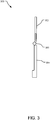
- FIG. 3 is a side view of a wireless communications device 300.
- first housing 302 and second housing 304 are pivotally joined via a separation interface, hinge assembly 306.
- Second housing 304 is approximately twice as thick at the lower end to accommodate a display (not shown), and first housing 302 is accordingly shorter than second housing 304 to permit a flush surface between first housing 302 and the display when the device 300 is in the closed position.
- hinge assembly 306 extends beyond the tops of first housing 302 and second housing 304 as shown in FIG. 4 , another side view of wireless communications device 400, illustrating first housing 402 mating with second housing 404 by pivoting around separation interface hinge assembly 406.
- FIG. 5 is a schematic diagram of the contents of a wireless communications device 500.
- Wireless communication device 500 includes a first housing 502 and second housing 504 pivotally joined by separation interface hinge assembly 506.
- first housing 502 contains a first network communication protocol assembly.
- first network communication protocol assembly includes LTE antennas 510 communicatively coupled to an LTE modem 512.
- the first network communications assembly may include other types of antennas, such as 3G or other cellular antennas or any other type of communications protocol.
- multiple bands from LTE antennas 510 may be diplexed or triplexed into LTE modem 512 according to a single PCB trace rather than via a coaxial cable as explained in more detail below with reference to Figs. 6-8 .
- LTE antennas 510 may be located on the same side of a printed circuit board.
- First housing 502 may contain memory device 514, processor 516, and additional memory device 518 including without limitation a dual SIM, nano SIM, or flash storage.
- the elements shown in this implementation contained in first housing 502 are electronically coupled to the elements contained in second housing 504 via a flex circuit across hinge assembly 506 (not shown).
- the flex circuit may include a flexible substrate with one or more printed circuits on one or both sides of the substrate, and may electronically connect any component housed in first housing 502 to any component housed in second housing 504.
- Second housing 504 contains, in this implementation, elements including battery 520, battery charger 528, and a second network communications assembly 522, 524, 526.
- the second network communications assembly includes USB port 526, which may be a USB-C port, Wi-Fi unit 524, and Wi-Fi antennas 522.
- Second network communications assembly may also include network interfaces to any other type of communications protocol.
- a user of device 500 connects a personal computing device to the wireless communications device 500 via second network assembly 522, 524, 526.
- the user of a personal computing device may connect via a wired connection to USB port 526 or via a wireless connection to Wi-Fi unit 524.
- Second housing 504 also in this implementation includes a display 504.
- a power switch to enable the user to power the device on and off may be incorporated into display 508.
- battery 520 may be a 1500 mAh battery.
- LTE antennas 510 may have dimensions of 20mm by 15mm with a 20mm separation.
- LTE modem may measure 1,240mm 2 .
- Memory 514 may measure 240mm 2 .
- Wi-Fi antennas 508 may measure 15mm by 8mm or, in the case of antennas that support only the 5 GHz band, and not 2.4 GHz, Wi-Fi antennas may measure 5mm by 3mm.
- FIG. 6 illustrates another example wireless communications device 600.
- antennas 602 may be communicatively coupled to a single printed circuit board (PCB) transmission line trace, which eliminates the need for a coaxial cable and does not suffer from issues related to the use of multiple transmission line traces such as configurations where the antennas 602 are located at different physical distances from the modem or transceiver.
- the antenna interface is communicatively coupled to at least one antenna feed and may be configured to filter frequency bands from an antenna signal received from at least one antenna.
- the antennas are further configured to amplify each of the frequency bands and multiplex the filtered and amplified frequency bands so that all of the frequency bands may share a single transmission line trace.
- wireless communications device 600 includes antennas 602, a switch bank circuitry 608, an LTE modem 606, antenna interfaces 606, and transmission line traces 610.
- the antennas 602 may be a main or a diversity antenna of the wireless communications device 600.
- a main or primary antenna is an antenna that transmits and receives wireless signals to and from base stations, satellites, and other wireless communications systems.
- the antenna interfaces 606 include a combination of one or more filters and low noise amplifiers (LNAs) that are communicatively coupled to the antennas 602 and transmission line traces 610.
- LNAs low noise amplifiers
- the antenna interfaces 606 may be printed or constructed on a chip that may be installed between the antennas 602 and a transmission line trace using multiple communication interfaces (e.g., one or more ports) that allow for the communication of signals.
- the combination of one or more filters and low noise amplifiers on the antenna interfaces 606 allow for an antenna signal received from antennas 602 to be communicated across the transmission line trace 610 without significant insertion loss along the trace 606. Furthermore, the antenna interfaces 606 may allow the signals to be communicated between the antennas 602 and the switch bank circuitry without the use of a bulky coaxial cable. Because the antenna signal is transmitted along a single transmission line trace (e.g., transmission line traces 610), issues related to using multiple traces may be eliminated.
- the switch bank circuitry 608 is a system of discrete electronic components configured to selectively communicate sub-bands of the frequency bands (e.g., high, middle, and low frequency bands) to and from the LTE modem 606 or to and from a transceiver.
- switch bank circuitry 608 may receive an antenna signal from the transmission line trace 610 and selectively communicate a desired sub-band of the antenna signal to an interface (not shown) at the LTE modem 606.
- a sub-band signal path 612 may include a band-pass filter (not shown), which is used to pass the selected frequencies within a certain range to the LTE modem 606 or to a transceiver.
- the LTE modem 606 and/or transceiver receives sub-bands of antenna signals from the switch bank circuitry 608 and sends sub-bands of antenna signals from communication channels of the wireless communications device 600 to the switch bank circuitry 608.
- the LTE modem 606 and/or transceiver is communicatively coupled to the communications channels of the wireless communications device 600 such as Wi-Fi antennas a Wi-Fi subsystem, a USB port, or any other communications assembly of the wireless communications device 600.
- wireless communications device 600 is shown having only one LTE modem 606 and/or transceiver, but it should be understood that the device may have more than one LTE modem or transceiver and it may have more than one type of modem and/or transceiver.
- FIG. 7 is a detail view schematic of an antenna subsystem with multiple bands triplexed into a single PCB trace connected to an LTE modem.
- the circuitry 700 can be designed on a chip or may be constructed on a printed circuit board assembly (PCBA).
- the circuitry 700 includes a full band antenna 702, an antenna interface circuitry 722, a transmission line trace 714, a radiofrequency (RF) switch bank 716, and a transceiver and/or LTE modem 720.
- RF radiofrequency
- the full band antenna 702 may be a three feed antenna that may send and receive high, middle, and low RF bands of antenna signals.
- the antenna is illustrated as being a single component but it should be understood that the antenna 702 may use a combination of single and/or multifeed antennas.
- the antenna interface circuitry 722 may include a number of filters (e.g., filters 724, 726, and 728) and three low noise amplifiers (LNAs) (e.g., LNAs 730, 732, and 734), each LNA configured for a particular frequency band of antenna signal.
- the antenna interface circuitry 722 may be communicatively coupled to the antenna 702 and transmission line trace 714 via one or more ports (e.g., ports 734 and 736) or other communications interfaces.
- the antenna interface circuitry 722 may be printed on a chip.
- the filters (e.g., 724, 726, and 728) may be RLC (resistor-inductor-capacitor) circuit configured to filter a particular frequency band from an antenna signal received from antenna 702.
- filters 724, 726, and 728 form a triplexer 704 that receives an antenna signal from the full band antenna 702 and filters the antenna signal to yield three separate signals: a filtered high band RF signal that is directed to a signal path 738; a filtered middle band signal that is directed to a signal path 740; and a filtered low band RF signal that is directed to a signal path 742.
- the LNA 706 is a high band LNA that receives the filtered high band RF signal from the triplexer 704 and amplifies the filtered high band RF and transmits the amplified high band RF signal to three filters (e.g., filters 730, 732, and 734) that form triplexer 712.
- the LNA 708 is a middle band LNA that receives the filtered middle band RF signal from the triplexer 704 and amplifies the filtered middle band RF signal, and transmits the amplified filtered middle band RF signal to the triplexer 712.
- the LNA 710 is a low band LNA that receives the filtered low band RF signal from the triplexer 704 and transmits the amplified filtered low band RF signal to the triplexer 712.
- the triplexer 712 receives each of the three amplified filtered band RF signals and multiplexes the three signals and outputs the signals to the transmission line trace 714.
- the triplexer 712 may be directly coupled to the transmission line trace 714 or may be coupled to transmission line trace 714 via a port or other communication interface (e.g., the port 734). Because each separate filtered frequency band is amplified and then multiplexed, there may be less noise in the signal when compared to other configurations.
- the transmission line trace 714 is a conductive trace that electrically connects the triplexer 712 with the RF switch bank 716.
- the transmission line trace 714 may be part of a printed circuit board assembly (PCBA). Because of the configuration of the antenna interface circuitry 722, all three of the filtered amplified frequency bands of antenna signals are able to use the transmission line trace 714. This configuration may significantly reduce insertion loss of the signal without the use of a bulky coaxial cable.
- the transmission line trace 714 is communicatively coupled to the switch bank circuitry 716.
- the switch bank circuitry 716 is a system of discrete electronic components configured to selectively communicate sub-bands of the frequency bands (e.g., high, middle, and low frequency bands) to and from LTE modem 720 and/or a transceiver.
- switch bank circuitry 716 may receive an antenna signal from the transmission line trace 714 and selectively communicate a desired sub-band of the antenna signal to a port at the LTE modem 720 and/or transceiver.
- a sub-band signal path may include one or more band-pass filters 718, which are used to pass the selected frequencies within a certain range to the LTE modem 720 and/or transceiver.
- more than one antenna 702 may be communicatively coupled to circuitry 722.
- a high- and middle-band antenna may be diplexed into filters 724 and 726 via a first port and a low-band antenna may be coupled to filter 728 via a second port.
- the three antenna signals may then be triplexed via triplexer 712 into the single transmission line trace 714.
- FIG. 8 is a schematic diagram of a wireless communications device 800 with LTE antennas 808 disposed in a first housing 802.
- Wireless communication device 800's antennas 808 may be spiral feed MIMO monopole antennas including without limitation a grounded coupling structure.
- Antennas 808 may in other implementations include PIFA antennas, dielectrics, loops, capacitive coupled antennas, inductive coupled antennas, apertune tuned antennas, and/or adaptive matching antennas.
- the first housing 802 is pivotally joined via hinge assembly 806 to a second housing 804.
- Wireless communication device 800 includes antenna interface circuitry 810 such as the antenna interface circuitry described with respect to FIG. 7 disposed on a first housing 802.
- Antenna interface circuitry 810 may include with multiple bands triplexed or diplexed into a single PCB trace connected to an LTE modem 814 and/or transceiver via a switching assembly 816 and one or more band-pass filters 818.
- FIG. 9 is a side view of a wireless communications device 900 with heat dissipating spreaders.
- Contents of wireless communications device 900 such as an LTE modem inside housing 902 or a battery system and/or a network communications assembly in second housing 904 could generate heat during operation. As the operating specifications for these components have upper temperature limits, it may be necessary to introduce active or passive cooling features into device 900.
- a first heat dissipating plate 910 may be included in first housing 902
- a second heat dissipating plate 914 may be included in second housing 904, and/or a third heat dissipating plate 912 in separation interface hinge assembly 906.
- first heat dissipating plate 914 may be a 0.15mm Copper spreader
- second heat dissipation plate 914 may be a 0.2mm Copper spreader
- third heat dissipation plate 912 may be a 0.2mm Copper connector.
- Third heat dissipation plate 912 is in thermal contact with first heat dissipation plate 910 and/or second heat dissipation plate 914.
- connecting wire 908 may include a thermally conductive element to create a thermal connection between first heat dissipation plate 910 and second heat dissipation plate 914.
- first housing 902 and second housing 904 may also be increased to facilitate cooling of the components housed therein.
- angle between first housing 902 and second housing 904 must be at least 45° to permit operation of foldable wireless communications device 900.
- hinge assembly 906 is a heat sink formed of materials with higher thermal conductivities than the first housing 902 and second housing 904. In this configuration, heat can flow to hinge assembly 906 via first housing 902 and second housing 904 or via thermal dissipation plates placed therein.
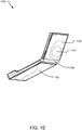
- FIG. 10 is a thermal view one side of a wireless communications device 1000 in operation.
- the thermal view illustrates a sample range of temperatures during operation across the surfaces of wireless communications device 1000. In an implementation, these temperatures were observed to range from 29.2 degrees Celsius to 56.7 degrees Celsius.
- a solid temperature of approximately 54.350 degrees Celsius was observed in the region 1004 on the back of wireless communications device 1000.
- Another solid temperature of approximately 49.807 was observed in region 1006, and a solid temperature of approximately 49.101degrees Celsius was observed in the region 1002.
- a locus of relatively higher temperature is centered on region 1004 with lower temperatures in the surrounding areas.
- a separation interface, hinge assembly 1008, is implemented as a heat sink relative to the two adjoining housings, and maintains a solid temperature roughly the same as the adjacent portions of the adjoining housings with which it is in thermal contact.
- FIG. 11 is another thermal view of wireless communications device 1100 in operation.
- solid temperatures were observed in the range of approximately 29.2 to 56.7 degrees Celsius.
- a local maximum solid temperature of approximately 55.795 degrees Celsius was observed in the region 1106 with lower solid temperatures in the surrounding regions.
- Solid temperatures of approximately 50.153 degrees Celsius and approximately 48.285 degrees Celsius were observed in the regions 1102 and 1104, respectively.
- Regions 1102 and 1004 are also roughly local maximums with the surrounding regions measuring lower relative solid temperatures as indicated by the heat map lines of FIG. 11 .
- FIG. 12 is a side view of another implementation of a wireless communications device 1200.
- Wireless communications device 1200 includes a first housing 1202 disposed above a second housing 1204. The two housings are moveable with respect to each other around a separation interface 1206 from a closed position into an open position as shown in FIG. 12 .
- Separation interface 1206 permits slidable movement in direction 1208 of first housing 1202 with respect to second housing 1204.
- separation interface 1206 further permits vertical movement 1206 of first housing 1202 with respect to second housing 1204, such that the two housings sit flush with respect to one another.
- separation interface 1206 may be a cantilever interface to facilitate movement of wireless communications device 1200 between the open and closed positions.
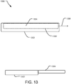
- FIG. 13 is a side view of another implementation of a wireless communications device 1300.
- Wireless communications device 1300 includes a second housing 1304 dispose inside of a first housing 1302.
- wireless communications device 1300 includes a separation interface 1308 to facilitate movement of second housing 1304 in direction 1306 with respect to first housing 1302. Separation interface 1308 may slidably couple the two housings using a friction fit and track interface between the two housings. In the open position, second housing 1304 may extend partially or completely beyond the end of first housing 1302 in direction 1306 as shown in FIG. 13 .
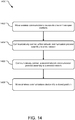
- FIG. 14 illustrates example operations 1400 for providing network data communications to a personal computing device via a wireless communications device.
- one or more antennas, an LTE modem, and/or Wi-Fi antennas may provide network data communications to the personal computing device.
- a moving operation 1402 moves a wireless communications device into one or more open positions.
- a user of the wireless communications device may manually move the device into one or more open positions.
- a hinge assembly may move a first housing including at least a first network communication protocol assembly with respect to a second housing including at least a second network communications protocol assembly.
- a separation interface may move a first housing including at least a first network communication protocol assembly with respect to a second housing including at least a second network communications protocol assembly.
- the wireless communications device may be moveable according to a separation interface, including without limitation a hinge assembly, a cantilever assembly, a friction fit interface, and/or a track and roller interface.
- the wireless communications device includes at least a first network communications protocol assembly with one or more antennas or ports configured to communicatively connect to a first network according to the first network protocol.
- a connecting operation 1404 communicatively connects the first network communications protocol to the first network.
- the first network protocol assembly may be an LTE modem and a plurality of LTE antennas.
- the LTE modem may communicatively connect the first network communication protocol assembly to a first network.
- the first network communications assembly may be connected in a number of ways.
- the device may execute instructions stored on an onboard memory to connect to available wireless networks automatically upon detection.
- the wireless communications device may cause a control panel interface to appear on a connected personal computing device to display a user interface suitable for controlling the wireless communications device and receiving user input to cause the LTE modem to connect to an available wireless data network.
- the wireless communications device includes at least a second network communications protocol assembly with one or more antennas or ports configured to communicatively connect to a second network according to the second network protocol, which is a network protocol different from the first network protocol.
- Another connecting operation 1406 communicatively connect the second network communication protocol assembly to the second network.
- the second network communications assembly connects to a personal computing device according to a Wi-Fi protocol.
- the second network communications assembly may be connected by a user selecting a Wi-Fi SSID broadcast by the wireless communications device on a personal computing device desired to be connected. A user may select the Wi-Fi network manually according to the interface of the personal computing device.
- the user may perform this connecting operation 1406 according other wireless communications protocols in the same way, such as Bluetooth or NFC.
- the user may connect the second network communications assembly to a personal computing device by configuring the personal computing device to automatically connect to Wi-Fi networks that have been previously connected to the device such as a Wi-Fi network broadcast by the wireless communications device.
- a moving operation 1408 moves the wireless communications device into a closed position.
- FIG. 15 illustrates example operations for 1500 manufacturing a wireless communications device.
- a connection operation 1502 connects a first housing to an LTE modem and a plurality of LTE antennas. Manufacturing devices including injection molding, extruding, and/or other manufacturing devices may perform connection operation 1502 and/or other connecting operations disclosed herein.
- the first housing may be formed of materials including black plastic or polycarbonate. In an implementation, the first housing may be formed using equipment including any one or more of a reactor, holding tank, centrifuge, demineralizer, concentrator, extruder, and pelletizer. The polycarbonate material may be extruded into the desired shape of the first.
- Another connection operation 1504 connects a second housing to at least one network assembly. Manufacturing devices including injection molding, extruding, and/or other manufacturing devices may perform connection operation 1504 and/or other connecting operations disclosed herein.
- Yet another connecting operation 1506 connects the first housing to the second housing movably via a separation interface, such that the first housing and second housing move with respect to each other between a closed position and one or more open positions.
- the one or more open positions may be characterized by an increased thermal separation between the components disposed within the first and second housings, respectively.
- the separation interface is a hinge assembly.
- the hinge may be constructed according any rotational hinge designs including a free fit or friction fit design.
- Manufacturing a wireless communications device may further include any combination of attaching a first thermal dissipation plate, a second heat dissipation plate, and/or a third heat dissipation plate to the first housing, second housing, and/or hinge assembly, respectively.
- Making a wireless communications device may further include forming one or more heat vent openings in the body of the first and/or second housings.
- Manufacturing a wireless communications device may further include forming a second housing including a display screen and/or a power switch, which may be integrated into, or a part of, the display screen.
Landscapes
- Engineering & Computer Science (AREA)
- Computer Networks & Wireless Communication (AREA)
- Microelectronics & Electronic Packaging (AREA)
- Signal Processing (AREA)
- Manufacturing & Machinery (AREA)
- Physics & Mathematics (AREA)
- Thermal Sciences (AREA)
- Telephone Set Structure (AREA)
- Transceivers (AREA)
- Mobile Radio Communication Systems (AREA)
Description
-
US 2014/0135060 A1 describes antenna placement techniques. A computing device includes an antenna suite having multiple different kinds of antennas. An antenna zone for the antenna suite may be established along a particular edge of the computing device. Non-interfering materials (e.g., RF transparent material) may be used within the antenna zone and other materials (e.g., metal) may be employed for other regions of the device. The multiple different kinds of antennas in the antenna suite may then be disposed within the established antenna zone. The antennas may be placed to minimize interference between antennas and/or achieve performance objective for the suite of antennas. -
US 2011/0045881 A1 describes a wireless communication module, comprising a substrate and at least one wireless module, disposed on the substrate. A portable device has a display part comprising a communication module, and a host part coupled to the display part. The communication module is deposited on top of the display part. -
US 2012/0224329 A1 describes a portable electronic device including a circuit board, a heat sink, a hinge and a heat dissipating plate. The circuit board is equipped with a heat generating component. The heat sink is for dissipating heat generated by the heat generating component. The heat dissipating plate is pivotably connected to the heat sink by the hinge for helping with the heat dissipation of the heat sink. -
US 2009/0207569 A1 describes a portable electronic apparatus including a first unit, a second unit, and a hinge unit. The first unit includes a first housing, a heat generating component inside the first housing, a first heat diffusing member disposed inside the first housing and diffusing heat from the heat generating component, and a heat dissipating part dissipating heat diffused by the first heat diffusing member to the outside of the first housing. The second unit includes a second housing, a second heat diffusing member disposed inside the second housing and diffusing heat inside the second housing, and a heat receiving part conducting heat from the heat dissipating part to the second heat diffusing member upon the heat receiving part being in contact with the heat dissipating part. -
US 2004/0042184 A1 describes an electronic apparatus including a housing which accommodates a heat generating component. A heat receiving portion thermally connected to the heat generating component is connected to a heat radiating portion via a circulating path through which a liquid coolant is circulated. The housing accommodates a heat sink which is separate from the heat radiating portion, and a fan. Part of heat from the heat generating component conducted to the heat receiving portion is conducted to the heat sink via a heat transferring member. The fan blows a cooling air against the heat sink. -
US 2007/146212 A1 ,US 2012/120322 A1 ,US 2014/333504 A1 disclose various ways for achieving a multi-band operation of an antenna. -
WO 2014/014140 A1 discloses a wireless router device which can be attached to the back of a wireless terminal. - The invention is defined by the appended claims.
-
FIG. 1 illustrates an example folding wireless communications device. -
FIG. 2 illustrates an alternative implementation of a folding wireless communications device. -
FIG. 3 is a side view of an implementation of a folding wireless communications device. -
FIG. 4 is another side view of an implementation of a folding wireless communications device. -
FIG. 5 is a schematic diagram of the contents of a folding wireless communications device. -
FIG. 6 illustrates another example folding wireless communications device. -
FIG. 7 illustrates an example circuitry for signal transmission between at least one antenna and a transceiver of a wireless communications device. -
FIG. 8 is a schematic diagram of a wireless communications device including spiral feed monopole LTE antennas with a grounded coupled structure with multiple bands triplexed into a single PCB trace connected to an LTE modem. -
FIG. 9 is a side view of a wireless communications device with heat dissipating spreaders. -
FIG. 10 is a thermal view one side of a folding wireless communications device in operation. -
FIG. 11 is a thermal view of another side of a folding wireless communications device in operation. -
FIG. 12 is a side view of another implementation of a wireless communications device. -
FIG. 13 is a side view of another implementation of a wireless communications device. -
FIG. 14 illustrates example operations for providing network data communications to a personal computing device via a wireless communications device. -
FIG. 15 illustrates example operations for manufacturing a wireless communications device. - Personal computing devices including laptops and tablets may not have onboard wireless data capabilities, such as 3G or LTE transceivers and antennas, and are therefore connected to the Internet when the devices have access to Local Area Networks (LANs), such as via Wi-Fi or wired Ethernet. To extend the range of network connectivity for these devices, a user may connect the device to a mobile data network using a wireless communications device, also known as a wireless hotspot. The connection between the personal computing device and the wireless communications device may be affected through a USB port such as a USB-C port, wirelessly (such as via a Wi-Fi network established by the wireless communications device), via a Bluetooth connection, or according to other wired or wireless protocols.
- A wireless communications device disclosed herein provides a worldwide LTE mobile wireless data connection to personal computing devices in a very small form factor. Worldwide connectivity and a small form factor may be accomplished using double-band or triple-band LTE antennas diplexed or triplexed, respectively, into an LTE modem via a single PCB trace instead of a coaxial cable to economize the consumption of physical space on the device. Further, the small form factor may be permitted by locating heat-producing or interfering components in separate housings moveable with respect to each other between a closed position and one or more open positions. Moving the wireless communications device from the closed position to the one or more open positions physically separates the two housings and one or more of the heat-producing or interfering components contained therein. By moving the wireless communications device into the one or more open positions, the physical separation of the housings decreases thermal proximity between potentially heat-producing components, such as a battery, battery charger, antenna(s), transceiver(s), and/or modem(s), and other on board electronics. The one or more open positions permits improved cooling due to increased air or surface contact on the housings that may be further improved according to active or passive cooling systems as described herein. The physical separation of the housings and components contained therein further reduces or eliminates undesirable interference between components disposed in the housings.
- In one implementation, the wireless communications device is a clamshell design including two housings pivotally joined at a hinge assembly. In an implementation, the wireless communications device is closed when the two housings are in contact lengthwise and angle at the hinge assembly is approximately zero degrees. The wireless communications device is in the one or more open positions when the angle measured in degrees between the first and second housings is nonzero. In other implementations, the housings of the wireless communications device are slideably coupled, such that a housing is disposed above another housing in the closed position, and the housings are disposed substantially adjacent to one another lengthwise in the one or more open positions. In another implementation, a housing is enclosed inside another housing when the wireless communications device is in the closed position, and the housings are slideably coupled, such that a housing extends partially or completely beyond the distal end of another housing in the open position.
- The wireless communications device : employs additional heat dissipation materials such as copper spreaders on the first and second housings. For further heat dissipation, the hinge assembly may be formed from a thermally conductive material to act as a heat sink with respect to the first and second housings or the hinge assembly may contain heat dissipation materials, such as a copper spreader in thermal contact with either one or both of the copper spreaders on the first and second housings.
- The wireless communications device may advantageously allow a memory for on board storage of user files received via a wired or wireless connection to the personal computing device. The wireless communications device may contain a processor configured to execute code stored on the memory such as operating system code or code downloaded to the hot spot over a digital communications channel. The wireless communications device may further advantageously contain a glass display to determine or display to the user any of the following: the power status of the battery, the current wireless data signal strength, the name of the current wireless carrier, or a current network throughput.
-
FIG. 1 illustrates an examplewireless communications device 100 that includes afirst housing 102 and asecond housing 104 pivotally joined by a separation interface. In an implementation, the separation interface ishinge assembly 106. In the implementation ofFIG. 1 ,hinge assembly 106 permits the movement offirst housing 102 andsecond housing 104 with respect to each other through an angle (e.g.,angles 108, 110) in a "clamshell" configuration. In this implementation,angles hinge assembly 106 are available, such as the approximately 110° ofangle 108 shown inFIG. 1 . In the closed position corresponding to a 0° angle ofhinge assembly 106, the hinge assembly extends beyond the edge offirst housing 102 andsecond housing 104. -
First housing 102 andsecond housing 104 may be constructed from a variety of suitable materials. In one implementation,first housing 102 andsecond housing 104 are polycarbonate. In another implementation,first housing 102 andsecond housing 104 are formed from black plastic.Hinge assembly 106 may also be constructed from polycarbonate or black plastic. In an implementation,hinge assembly 106 is a heat sink relative tofirst housing 102 andsecond housing 104 and may be constructed from a material with a higher thermal conductivity than the materials used to constructfirst housing 102 andsecond housing 104. Heat dissipation inwireless communications device 100 is explained in more detail below with reference toFIG. 9 . - In an implementation,
second housing 104 includes adisplay 112 for displaying information relevant to the wireless communications device to a user including a mobile signal strength indicator, a battery level indicator, the name of a wireless carrier, a network throughput indicator, and a connectivity indicator indicating whether and how the wireless communications device is communicatively connected to a personal computing device. In an alternative implementation,wireless communications device 100 may cause the display of the aforementioned relevant information on the screen of a connected personal computing device instead of ondisplay 112. In the implementation shown inFIG. 1 , the portion ofsecond housing 104 includingdisplay 112 is approximately twice as thick asfirst housing 102, and creates a flush surface betweenfirst housing 102 anddisplay 112 when the angle of hinge assembly 105 is approximately 0°, corresponding to the closed position ofwireless communications device 100.Display 112 may be enclosed in a black gloss or glass display housing. - In the implementation shown in
FIG. 1 ,display 112 is raised abovesecond housing 104 by an amount roughly equal to the thickness offirst housing 102 such that, whenwireless communications device 100 is in the closed position,display 112 andfirst housing 102 sit flush with respect to one another. In this implementation,second housing 104 may measure approximately 6mm by 72mm by 74.5mm, except in the area ofdisplay 112 where the thickness is double, approximately 12mm.First housing 102 in this implementation may measure 6mm by 72mm by an amount such thatfirst housing 102 and display 112 equal approximately 74.5 mm. Therefore whenwireless communications device 100 in this implementation is in the closed position, its dimensions are approximately 12mm by 72mm by 74.5mm and, whenwireless communications device 100 is in the fully open position, i.e., whenangle 108 equals approximately 180°, its dimensions are approximately 12mm by 72mm by 144mm. - In an implementation, a
display 112 may include a power switch. In another implementation, a dedicated power switch may activate the device. In yet another implementation, the device may be awoken or powered on remotely such as by connecting a cable or wirelessly via a Bluetooth connection, Wi-Fi connection, NFC communications, activation of an on board sensor such as an accelerometer, heat sensor, noise sensor, or temperature sensor. In yet another implementation, the wireless communications device may be powered on or awoken based on a timer or according to a date and time schedule, which may depend on one or more conditions such as remaining battery life or status of connected personal computing devices. The wireless communications device may include a position sensor that indicates the orientation of the first housing with respect to the second housing or indicates whether the angle between the two housings is greater than a predetermined minimum angle. For example, the position sensor could be activated if the angle between the first and second housings is greater than 45 degrees. In another implementation, the position sensor is a Hall effect sensor. -
FIG. 2 illustrates another implementation ofwireless communications device 200. In the implementation ofFIG. 2 , afirst housing 202 and asecond housing 204 are more rectangular with dimensions measuring 7.5mm by 90mm by 57mm for each housing.First housing 202 andsecond housing 204 are pivotally joined by a separation interface,hinge assembly 206, permitting rotation with respect to each other throughangle 210. Thewireless communications device 200 is closed whenangle 210 measures approximately 0°, and is in the one or more open positions whenangle 210 measures a nonzero number of degrees. Whenwireless communications device 200 is in the closed position in thisimplementation hinge assembly 206 extends beyond the edge offirst housing 202 andsecond housing 204. Thewireless communications device 200 is in the fully open position whenangle 210 measures approximately 180°. - In the implementation shown in
FIG. 2 ,second housing 204 integratesdisplay 208. One or both of the inward facing surfaces offirst housing 202 andsecond housing 204 may be formed of a transparent material such as a black gloss display lens to facilitateviewing display 208.Display 208 may display information relevant to the wireless communications device to a user including a mobile signal strength indicator, a battery level indicator, the name of a wireless carrier, a network throughput indicator, and a connectivity indicator indicating whether and how the wireless communications device is communicatively connected to a personal computing device. Display 208's integration intosecond housing 204 permits bothfirst housing 202 andsecond housing 204 to have approximately equal dimensions, in contrast to the implementation shown inFIG. 1 where the raiseddisplay 112 causessecond housing 104 to have a double thickness in the area ofdisplay 112 andfirst housing 102 is consequently shorter thansecond housing 104 by an amount suitable to permithousing 102 anddisplay 112 to sit flush whenwireless communications device 100 is in the closed position. -
FIG. 3 is a side view of awireless communications device 300. In this implementation,first housing 302 andsecond housing 304 are pivotally joined via a separation interface,hinge assembly 306.Second housing 304 is approximately twice as thick at the lower end to accommodate a display (not shown), andfirst housing 302 is accordingly shorter thansecond housing 304 to permit a flush surface betweenfirst housing 302 and the display when thedevice 300 is in the closed position. Also in the closed position, hingeassembly 306 extends beyond the tops offirst housing 302 andsecond housing 304 as shown inFIG. 4 , another side view ofwireless communications device 400, illustratingfirst housing 402 mating withsecond housing 404 by pivoting around separationinterface hinge assembly 406. -
FIG. 5 is a schematic diagram of the contents of awireless communications device 500.Wireless communication device 500 includes afirst housing 502 andsecond housing 504 pivotally joined by separationinterface hinge assembly 506. In this implementation,first housing 502 contains a first network communication protocol assembly. In an implementation, first network communication protocol assembly includesLTE antennas 510 communicatively coupled to anLTE modem 512. The first network communications assembly may include other types of antennas, such as 3G or other cellular antennas or any other type of communications protocol. In an implementation, multiple bands fromLTE antennas 510 may be diplexed or triplexed intoLTE modem 512 according to a single PCB trace rather than via a coaxial cable as explained in more detail below with reference toFigs. 6-8 .LTE antennas 510 may be located on the same side of a printed circuit board.First housing 502 may containmemory device 514,processor 516, andadditional memory device 518 including without limitation a dual SIM, nano SIM, or flash storage. The elements shown in this implementation contained infirst housing 502 are electronically coupled to the elements contained insecond housing 504 via a flex circuit across hinge assembly 506 (not shown). The flex circuit may include a flexible substrate with one or more printed circuits on one or both sides of the substrate, and may electronically connect any component housed infirst housing 502 to any component housed insecond housing 504. -
Second housing 504 contains, in this implementation,elements including battery 520,battery charger 528, and a secondnetwork communications assembly USB port 526, which may be a USB-C port, Wi-Fi unit 524, and Wi-Fi antennas 522. Second network communications assembly may also include network interfaces to any other type of communications protocol. A user ofdevice 500 connects a personal computing device to thewireless communications device 500 viasecond network assembly USB port 526 or via a wireless connection to Wi-Fi unit 524. Other types of connections to thesecond network assembly Second housing 504 also in this implementation includes adisplay 504. A power switch to enable the user to power the device on and off may be incorporated intodisplay 508. - In an implementation,
battery 520 may be a 1500 mAh battery.LTE antennas 510 may have dimensions of 20mm by 15mm with a 20mm separation. LTE modem may measure 1,240mm2.Memory 514 may measure 240mm2. Wi-Fi antennas 508 may measure 15mm by 8mm or, in the case of antennas that support only the 5 GHz band, and not 2.4 GHz, Wi-Fi antennas may measure 5mm by 3mm. -
FIG. 6 illustrates another examplewireless communications device 600. In this implementation,antennas 602 may be communicatively coupled to a single printed circuit board (PCB) transmission line trace, which eliminates the need for a coaxial cable and does not suffer from issues related to the use of multiple transmission line traces such as configurations where theantennas 602 are located at different physical distances from the modem or transceiver. The antenna interface is communicatively coupled to at least one antenna feed and may be configured to filter frequency bands from an antenna signal received from at least one antenna. The antennas are further configured to amplify each of the frequency bands and multiplex the filtered and amplified frequency bands so that all of the frequency bands may share a single transmission line trace. Antennas in this configuration may be positioned with respect to one another closer than 1/4 of the wavelength of the lowest frequency band supported by the LTE antennas. In this implementation,wireless communications device 600 includesantennas 602, aswitch bank circuitry 608, anLTE modem 606, antenna interfaces 606, and transmission line traces 610. - The
antennas 602 may be a main or a diversity antenna of thewireless communications device 600. A main or primary antenna is an antenna that transmits and receives wireless signals to and from base stations, satellites, and other wireless communications systems. The antenna interfaces 606 include a combination of one or more filters and low noise amplifiers (LNAs) that are communicatively coupled to theantennas 602 and transmission line traces 610. The antenna interfaces 606 may be printed or constructed on a chip that may be installed between theantennas 602 and a transmission line trace using multiple communication interfaces (e.g., one or more ports) that allow for the communication of signals. The combination of one or more filters and low noise amplifiers on the antenna interfaces 606 allow for an antenna signal received fromantennas 602 to be communicated across thetransmission line trace 610 without significant insertion loss along thetrace 606. Furthermore, the antenna interfaces 606 may allow the signals to be communicated between theantennas 602 and the switch bank circuitry without the use of a bulky coaxial cable. Because the antenna signal is transmitted along a single transmission line trace (e.g., transmission line traces 610), issues related to using multiple traces may be eliminated. - The
switch bank circuitry 608 is a system of discrete electronic components configured to selectively communicate sub-bands of the frequency bands (e.g., high, middle, and low frequency bands) to and from theLTE modem 606 or to and from a transceiver. For example,switch bank circuitry 608 may receive an antenna signal from thetransmission line trace 610 and selectively communicate a desired sub-band of the antenna signal to an interface (not shown) at theLTE modem 606. Furthermore, a sub-band signal path 612 may include a band-pass filter (not shown), which is used to pass the selected frequencies within a certain range to theLTE modem 606 or to a transceiver. - The
LTE modem 606 and/or transceiver receives sub-bands of antenna signals from theswitch bank circuitry 608 and sends sub-bands of antenna signals from communication channels of thewireless communications device 600 to theswitch bank circuitry 608. TheLTE modem 606 and/or transceiver is communicatively coupled to the communications channels of thewireless communications device 600 such as Wi-Fi antennas a Wi-Fi subsystem, a USB port, or any other communications assembly of thewireless communications device 600.wireless communications device 600 is shown having only oneLTE modem 606 and/or transceiver, but it should be understood that the device may have more than one LTE modem or transceiver and it may have more than one type of modem and/or transceiver. - The above-described antenna configurations and interfaces can be used to transmit signals along a single transmission line trace without the use of a coaxial cable or multiple transmission line traces. These configurations and interfaces are described further with respect to
FIG. 7. FIG. 7 is a detail view schematic of an antenna subsystem with multiple bands triplexed into a single PCB trace connected to an LTE modem. It should be understood that thecircuitry 700 can be designed on a chip or may be constructed on a printed circuit board assembly (PCBA). Thecircuitry 700 includes afull band antenna 702, anantenna interface circuitry 722, atransmission line trace 714, a radiofrequency (RF)switch bank 716, and a transceiver and/orLTE modem 720. Thefull band antenna 702 may be a three feed antenna that may send and receive high, middle, and low RF bands of antenna signals. The antenna is illustrated as being a single component but it should be understood that theantenna 702 may use a combination of single and/or multifeed antennas. - The
antenna interface circuitry 722 may include a number of filters (e.g., filters 724, 726, and 728) and three low noise amplifiers (LNAs) (e.g.,LNAs antenna interface circuitry 722 may be communicatively coupled to theantenna 702 andtransmission line trace 714 via one or more ports (e.g.,ports 734 and 736) or other communications interfaces. Theantenna interface circuitry 722 may be printed on a chip. The filters (e.g., 724, 726, and 728) may be RLC (resistor-inductor-capacitor) circuit configured to filter a particular frequency band from an antenna signal received fromantenna 702. In this example implementation, filters 724, 726, and 728 form atriplexer 704 that receives an antenna signal from thefull band antenna 702 and filters the antenna signal to yield three separate signals: a filtered high band RF signal that is directed to asignal path 738; a filtered middle band signal that is directed to asignal path 740; and a filtered low band RF signal that is directed to asignal path 742. - In this example implementation, the
LNA 706 is a high band LNA that receives the filtered high band RF signal from thetriplexer 704 and amplifies the filtered high band RF and transmits the amplified high band RF signal to three filters (e.g., filters 730, 732, and 734) that formtriplexer 712. TheLNA 708 is a middle band LNA that receives the filtered middle band RF signal from thetriplexer 704 and amplifies the filtered middle band RF signal, and transmits the amplified filtered middle band RF signal to thetriplexer 712. TheLNA 710 is a low band LNA that receives the filtered low band RF signal from thetriplexer 704 and transmits the amplified filtered low band RF signal to thetriplexer 712. Thetriplexer 712 receives each of the three amplified filtered band RF signals and multiplexes the three signals and outputs the signals to thetransmission line trace 714. Thetriplexer 712 may be directly coupled to thetransmission line trace 714 or may be coupled totransmission line trace 714 via a port or other communication interface (e.g., the port 734). Because each separate filtered frequency band is amplified and then multiplexed, there may be less noise in the signal when compared to other configurations. - The
transmission line trace 714 is a conductive trace that electrically connects thetriplexer 712 with theRF switch bank 716. Thetransmission line trace 714 may be part of a printed circuit board assembly (PCBA). Because of the configuration of theantenna interface circuitry 722, all three of the filtered amplified frequency bands of antenna signals are able to use thetransmission line trace 714. This configuration may significantly reduce insertion loss of the signal without the use of a bulky coaxial cable. - The
transmission line trace 714 is communicatively coupled to theswitch bank circuitry 716. Theswitch bank circuitry 716 is a system of discrete electronic components configured to selectively communicate sub-bands of the frequency bands (e.g., high, middle, and low frequency bands) to and fromLTE modem 720 and/or a transceiver. For example,switch bank circuitry 716 may receive an antenna signal from thetransmission line trace 714 and selectively communicate a desired sub-band of the antenna signal to a port at theLTE modem 720 and/or transceiver. Furthermore, a sub-band signal path may include one or more band-pass filters 718, which are used to pass the selected frequencies within a certain range to theLTE modem 720 and/or transceiver. - In another implementation, more than one
antenna 702 may be communicatively coupled tocircuitry 722. For example, a high- and middle-band antenna may be diplexed intofilters triplexer 712 into the singletransmission line trace 714. -
FIG. 8 is a schematic diagram of awireless communications device 800 withLTE antennas 808 disposed in afirst housing 802.Wireless communication device 800'santennas 808 may be spiral feed MIMO monopole antennas including without limitation a grounded coupling structure.Antennas 808 may in other implementations include PIFA antennas, dielectrics, loops, capacitive coupled antennas, inductive coupled antennas, apertune tuned antennas, and/or adaptive matching antennas. Thefirst housing 802 is pivotally joined viahinge assembly 806 to asecond housing 804.Wireless communication device 800 includesantenna interface circuitry 810 such as the antenna interface circuitry described with respect toFIG. 7 disposed on afirst housing 802.Antenna interface circuitry 810 may include with multiple bands triplexed or diplexed into a single PCB trace connected to an LTE modem 814 and/or transceiver via a switchingassembly 816 and one or more band-pass filters 818. -
FIG. 9 is a side view of awireless communications device 900 with heat dissipating spreaders. Contents ofwireless communications device 900 such as an LTE modem insidehousing 902 or a battery system and/or a network communications assembly insecond housing 904 could generate heat during operation. As the operating specifications for these components have upper temperature limits, it may be necessary to introduce active or passive cooling features intodevice 900. - In one implementation, a first
heat dissipating plate 910 may be included infirst housing 902, a secondheat dissipating plate 914 may be included insecond housing 904, and/or a thirdheat dissipating plate 912 in separationinterface hinge assembly 906. In an implementation, firstheat dissipating plate 914 may be a 0.15mm Copper spreader, secondheat dissipation plate 914 may be a 0.2mm Copper spreader, and thirdheat dissipation plate 912 may be a 0.2mm Copper connector. Thirdheat dissipation plate 912 is in thermal contact with firstheat dissipation plate 910 and/or secondheat dissipation plate 914. In anotherimplementation connecting wire 908 may include a thermally conductive element to create a thermal connection between firstheat dissipation plate 910 and secondheat dissipation plate 914. - The angle between
first housing 902 andsecond housing 904 may also be increased to facilitate cooling of the components housed therein. In one implementation the angle betweenfirst housing 902 andsecond housing 904 must be at least 45° to permit operation of foldablewireless communications device 900. - In another implementation,
hinge assembly 906 is a heat sink formed of materials with higher thermal conductivities than thefirst housing 902 andsecond housing 904. In this configuration, heat can flow to hingeassembly 906 viafirst housing 902 andsecond housing 904 or via thermal dissipation plates placed therein. -
FIG. 10 is a thermal view one side of awireless communications device 1000 in operation. The thermal view illustrates a sample range of temperatures during operation across the surfaces ofwireless communications device 1000. In an implementation, these temperatures were observed to range from 29.2 degrees Celsius to 56.7 degrees Celsius. In the implementation ofFIG. 10 , a solid temperature of approximately 54.350 degrees Celsius was observed in theregion 1004 on the back ofwireless communications device 1000. Another solid temperature of approximately 49.807 was observed inregion 1006, and a solid temperature of approximately 49.101degrees Celsius was observed in theregion 1002. It should be appreciated from this thermal view that a locus of relatively higher temperature is centered onregion 1004 with lower temperatures in the surrounding areas. It should also be appreciated that a separation interface,hinge assembly 1008, is implemented as a heat sink relative to the two adjoining housings, and maintains a solid temperature roughly the same as the adjacent portions of the adjoining housings with which it is in thermal contact. -
FIG. 11 is another thermal view ofwireless communications device 1100 in operation. In this implementation, solid temperatures were observed in the range of approximately 29.2 to 56.7 degrees Celsius. In this implementation, a local maximum solid temperature of approximately 55.795 degrees Celsius was observed in theregion 1106 with lower solid temperatures in the surrounding regions. Solid temperatures of approximately 50.153 degrees Celsius and approximately 48.285 degrees Celsius were observed in theregions Regions FIG. 11 . -
FIG. 12 is a side view of another implementation of awireless communications device 1200.Wireless communications device 1200 includes afirst housing 1202 disposed above asecond housing 1204. The two housings are moveable with respect to each other around aseparation interface 1206 from a closed position into an open position as shown inFIG. 12 .Separation interface 1206 permits slidable movement indirection 1208 offirst housing 1202 with respect tosecond housing 1204. In an implementation,separation interface 1206 further permitsvertical movement 1206 offirst housing 1202 with respect tosecond housing 1204, such that the two housings sit flush with respect to one another. In an implementation,separation interface 1206 may be a cantilever interface to facilitate movement ofwireless communications device 1200 between the open and closed positions. -
FIG. 13 is a side view of another implementation of awireless communications device 1300.Wireless communications device 1300 includes asecond housing 1304 dispose inside of afirst housing 1302. In an implementation,wireless communications device 1300 includes aseparation interface 1308 to facilitate movement ofsecond housing 1304 indirection 1306 with respect tofirst housing 1302.Separation interface 1308 may slidably couple the two housings using a friction fit and track interface between the two housings. In the open position,second housing 1304 may extend partially or completely beyond the end offirst housing 1302 indirection 1306 as shown inFIG. 13 . -
FIG. 14 illustratesexample operations 1400 for providing network data communications to a personal computing device via a wireless communications device. In implementations, one or more antennas, an LTE modem, and/or Wi-Fi antennas may provide network data communications to the personal computing device. A movingoperation 1402 moves a wireless communications device into one or more open positions. A user of the wireless communications device may manually move the device into one or more open positions. In implementations, a hinge assembly may move a first housing including at least a first network communication protocol assembly with respect to a second housing including at least a second network communications protocol assembly. In other implementations, a separation interface may move a first housing including at least a first network communication protocol assembly with respect to a second housing including at least a second network communications protocol assembly. The wireless communications device may be moveable according to a separation interface, including without limitation a hinge assembly, a cantilever assembly, a friction fit interface, and/or a track and roller interface. The wireless communications device includes at least a first network communications protocol assembly with one or more antennas or ports configured to communicatively connect to a first network according to the first network protocol. A connectingoperation 1404 communicatively connects the first network communications protocol to the first network. In an implementation, the first network protocol assembly may be an LTE modem and a plurality of LTE antennas. In implementations, the LTE modem may communicatively connect the first network communication protocol assembly to a first network. The first network communications assembly may be connected in a number of ways. The device may execute instructions stored on an onboard memory to connect to available wireless networks automatically upon detection. In an implementation, the wireless communications device may cause a control panel interface to appear on a connected personal computing device to display a user interface suitable for controlling the wireless communications device and receiving user input to cause the LTE modem to connect to an available wireless data network. - In one implementation, the wireless communications device includes at least a second network communications protocol assembly with one or more antennas or ports configured to communicatively connect to a second network according to the second network protocol, which is a network protocol different from the first network protocol. Another connecting
operation 1406 communicatively connect the second network communication protocol assembly to the second network. In one implementation, the second network communications assembly connects to a personal computing device according to a Wi-Fi protocol. In another implementation, the second network communications assembly may be connected by a user selecting a Wi-Fi SSID broadcast by the wireless communications device on a personal computing device desired to be connected. A user may select the Wi-Fi network manually according to the interface of the personal computing device. The user may perform this connectingoperation 1406 according other wireless communications protocols in the same way, such as Bluetooth or NFC. In an implementation, the user may connect the second network communications assembly to a personal computing device by configuring the personal computing device to automatically connect to Wi-Fi networks that have been previously connected to the device such as a Wi-Fi network broadcast by the wireless communications device. A movingoperation 1408 moves the wireless communications device into a closed position. -
FIG. 15 illustrates example operations for 1500 manufacturing a wireless communications device. Aconnection operation 1502 connects a first housing to an LTE modem and a plurality of LTE antennas. Manufacturing devices including injection molding, extruding, and/or other manufacturing devices may performconnection operation 1502 and/or other connecting operations disclosed herein. The first housing may be formed of materials including black plastic or polycarbonate. In an implementation, the first housing may be formed using equipment including any one or more of a reactor, holding tank, centrifuge, demineralizer, concentrator, extruder, and pelletizer. The polycarbonate material may be extruded into the desired shape of the first. Anotherconnection operation 1504 connects a second housing to at least one network assembly. Manufacturing devices including injection molding, extruding, and/or other manufacturing devices may performconnection operation 1504 and/or other connecting operations disclosed herein. - Yet another connecting
operation 1506 connects the first housing to the second housing movably via a separation interface, such that the first housing and second housing move with respect to each other between a closed position and one or more open positions. The one or more open positions may be characterized by an increased thermal separation between the components disposed within the first and second housings, respectively. In an embodiment, the separation interface is a hinge assembly. The hinge may be constructed according any rotational hinge designs including a free fit or friction fit design. Manufacturing a wireless communications device may further include any combination of attaching a first thermal dissipation plate, a second heat dissipation plate, and/or a third heat dissipation plate to the first housing, second housing, and/or hinge assembly, respectively. Making a wireless communications device may further include forming one or more heat vent openings in the body of the first and/or second housings. Manufacturing a wireless communications device may further include forming a second housing including a display screen and/or a power switch, which may be integrated into, or a part of, the display screen. - The above specification, examples, and data provide a complete description of the structure and use of exemplary embodiments of the invention. Since many embodiments of the invention can be made without departing from the scope of the invention, the invention resides in the claims hereinafter appended.
Claims (12)
- A wireless communications device comprising:a first housing (902) including an LTE modem (512) and a plurality of LTE antennas (510);a second housing (904) including at least one network communications assembly comprising a Wi-Fi unit (524) and Wi-Fi antennas (522),wherein a first thermal distribution plate (910) is affixed to the first housing and a second thermal distribution plate (914) is affixed to the second housing, andthe first housing (902) and second housing (904) are moveably joined via a separation interface (906) permitting movement of the first housing and second housing with respect to each other between a closed position and one or more open positions,wherein a third thermal distribution plate (912) is affixed to the separation interface (906) wherein the third thermal distribution plate (912) is thermally coupled to the first (910) and/or second (914) thermal distribution plate in at least one of the one or more open positions.
- The device of claim 1 wherein the plurality of LTE antennas are communicatively coupled via at least two feeds diplexed into a single PCB trace into the LTE modem.
- The device of claim 2 wherein the plurality of LTE antennas (808) are communicatively coupled via at least three feeds triplexed into a single PCB trace (812) into the LTE modem.
- The device of claim 1 wherein the separation interface is a hinge assembly (906).
- The device of claim 4 wherein the hinge assembly includes a flex circuit electronically coupling the contents of the first housing to the contents of the second housing.
- The device of claim 1 wherein the separation interface (906) is a heat sink between the first housing (902) and second housing (904).
- The device of claim 1 wherein the first housing and second housing each measure substantially 90mm in width by 57mm in length.
- The device of claim 1 wherein at least two of the plurality of LTE antennas are positioned with respect to one another closer than 1/4 of the wavelength of the lowest frequency band supported by the LTE antennas.
- The device of claim 1 wherein the wireless communications device includes a position sensor activated when the device is in the one or more open positions.
- The device of claim 1 wherein the first housing includes a memory operable to store digital files received from the personal computing device via the network communications assembly.
- A method of manufacturing a wireless communications device comprising:connecting (1502) a first housing to an LTE modem and a plurality of LTE antennas;connecting (1504) a second housing to at least one network communications assembly comprising a Wi-Fi unit (524) and Wi-Fi antennas (522);connecting (1506) the first housing to the second housing via a separation interface such that the first housing and second housing are moveable with respect to each other between a closed position and one or more open positions;
the method further comprising affixing a first thermal distribution plate to the first housing, affixing a second thermal distribution plate to the second housing, and affixing a third thermal distribution plate (912) to the separation interface (906) wherein the third thermal distribution plate (912) is thermally coupled to the first (910) and/or second (914) thermal distribution plate in at least one of the one or more open positions. - The method of claim 11 wherein a display (112) screen disposed in the second housing includes at least one of: a mobile signal strength indicator, a battery level indicator, the name of a wireless carrier, and a network throughput indicator.
Applications Claiming Priority (2)
| Application Number | Priority Date | Filing Date | Title |
|---|---|---|---|
| US15/001,093 US10778289B2 (en) | 2016-01-19 | 2016-01-19 | Wireless communications device |
| PCT/US2017/013574 WO2017127309A2 (en) | 2016-01-19 | 2017-01-13 | Wireless communications device |
Publications (2)
| Publication Number | Publication Date |
|---|---|
| EP3405993A2 EP3405993A2 (en) | 2018-11-28 |
| EP3405993B1 true EP3405993B1 (en) | 2021-03-03 |
Family
ID=58016800
Family Applications (1)
| Application Number | Title | Priority Date | Filing Date |
|---|---|---|---|
| EP17704576.2A Active EP3405993B1 (en) | 2016-01-19 | 2017-01-13 | Wireless communications device |
Country Status (4)
| Country | Link |
|---|---|
| US (2) | US10778289B2 (en) |
| EP (1) | EP3405993B1 (en) |
| CN (1) | CN108432039B (en) |
| WO (1) | WO2017127309A2 (en) |
Families Citing this family (6)
| Publication number | Priority date | Publication date | Assignee | Title |
|---|---|---|---|---|
| US10418829B2 (en) * | 2017-01-18 | 2019-09-17 | Futurewei Technologies, Inc. | Charger having retractable cooling surface |
| CN109167150B (en) * | 2018-08-29 | 2021-02-26 | Oppo广东移动通信有限公司 | Electronic equipment |
| CN112639671A (en) * | 2018-09-14 | 2021-04-09 | 深圳市柔宇科技股份有限公司 | Electronic device |
| WO2021045272A1 (en) | 2019-09-05 | 2021-03-11 | 엘지전자 주식회사 | Mobile terminal and auxiliary device coupled thereto |
| US11843185B2 (en) * | 2021-06-07 | 2023-12-12 | Dell Products L.P. | Distributed, tunable radiating element |
| EP4432046B1 (en) * | 2022-03-02 | 2025-12-10 | Samsung Electronics Co., Ltd. | Electronic device and method for displaying information of a plurality of batteries of the electronic device |
Family Cites Families (34)
| Publication number | Priority date | Publication date | Assignee | Title |
|---|---|---|---|---|
| US6469669B1 (en) * | 1999-02-16 | 2002-10-22 | Qualcomm Incorporated | Hybrid antenna system for a portable wireless communication device |
| US6392883B1 (en) * | 2000-06-30 | 2002-05-21 | Intel Corporation | Heat exchanger having phase change material for a portable computing device |
| JP3673249B2 (en) | 2002-08-27 | 2005-07-20 | 株式会社東芝 | Electronic equipment and cooling device |
| WO2005069757A2 (en) | 2004-01-12 | 2005-08-04 | Ortronics, Inc. | Wi-access point device and system |
| US7274340B2 (en) | 2005-12-28 | 2007-09-25 | Nokia Corporation | Quad-band coupling element antenna structure |
| US9941588B2 (en) * | 2007-08-20 | 2018-04-10 | Ethertronics, Inc. | Antenna with multiple coupled regions |
| JP4888413B2 (en) | 2008-02-14 | 2012-02-29 | 富士通株式会社 | Portable electronic device |
| US7746631B2 (en) * | 2008-08-29 | 2010-06-29 | Apple Inc. | Methods and apparatus for cooling electronic devices using thermally conductive hinge assemblies |
| JP2010067225A (en) * | 2008-09-12 | 2010-03-25 | Toshiba Corp | Information processor |
| CN101562864B (en) | 2009-05-12 | 2011-02-02 | 华为终端有限公司 | Hot spot device |
| JP2011015345A (en) | 2009-07-06 | 2011-01-20 | Panasonic Corp | Portable wireless device |
| US9058152B2 (en) | 2009-08-24 | 2015-06-16 | Ralink Technology Corporation | Wireless communication module, portable device using the same and method for manufacturing the same |
| USD654917S1 (en) | 2009-08-31 | 2012-02-28 | Novatel Wireless Inc. | Personal wireless hotspot device |
| TWI507116B (en) * | 2009-11-30 | 2015-11-01 | Radiation element and potable electronic device using same | |
| US8344836B2 (en) * | 2010-09-17 | 2013-01-01 | Apple Inc. | Protective cover for a tablet computer |
| CN102655729A (en) | 2011-03-02 | 2012-09-05 | 鸿富锦精密工业(深圳)有限公司 | Portable electronic device |
| CN102790872B (en) | 2011-05-20 | 2016-11-16 | 南京中兴软件有限责任公司 | Method and system for realizing video conferencing |
| US8860619B2 (en) | 2011-09-20 | 2014-10-14 | Netgear, Inc. | Wireless device and multi-antenna system having dual open-slot radiators |
| US9351237B2 (en) * | 2011-09-27 | 2016-05-24 | Z124 | Displaying of charging status on dual screen device |
| TWI430684B (en) | 2011-10-18 | 2014-03-11 | Quanta Comp Inc | Combinatorial mobile hotspot device and network service provision method, network access device and wireless service power supply device thereof |
| FI20116089A7 (en) | 2011-11-04 | 2013-05-05 | Lite On Mobile Oyj | An antenna arrangement and an electronic device |
| US9182794B2 (en) * | 2011-11-30 | 2015-11-10 | Google Inc. | Notebook metal hinge as heat sink element |
| US20130195088A1 (en) | 2012-01-30 | 2013-08-01 | Novatel Wireless, Inc. | Mobile hotspot device and battery |
| WO2014014140A1 (en) | 2012-07-18 | 2014-01-23 | (주)인포마크 | Case and assembly of wireless router and wireless terminal combined by means of case |
| CN102833878B (en) | 2012-08-20 | 2019-02-15 | 中兴通讯股份有限公司 | Mobile hotspot device and method for accessing network |
| US9148979B2 (en) * | 2012-10-08 | 2015-09-29 | Qualcomm Incorporated | Heat dissipating apparatus for folding electronic devices |
| US8654030B1 (en) | 2012-10-16 | 2014-02-18 | Microsoft Corporation | Antenna placement |
| GB2509519B (en) * | 2013-01-04 | 2018-02-14 | Broadcom Corp | Methods and apparatuses for managing acknowledgements |
| US20140253024A1 (en) | 2013-03-06 | 2014-09-11 | Nokia Corporation | Method and apparatus for wirelessly charging mobile devices |
| KR101712976B1 (en) * | 2013-06-26 | 2017-03-22 | 인텔 아이피 코포레이션 | Bulk acoustic wave resonator tuner circuits |
| US10230424B2 (en) * | 2013-09-23 | 2019-03-12 | Maxlinear, Inc. | Microwave backhaul system supporting multiple installation configurations |
| US9398637B2 (en) | 2013-11-21 | 2016-07-19 | Apple Inc. | Hotspot device |
| US8843178B1 (en) | 2014-01-28 | 2014-09-23 | Gigastone America Corp | Wireless hotspot device capable of sharing video picture |
| US9513672B2 (en) * | 2015-05-05 | 2016-12-06 | Apple Inc. | Electronic device with dynamic hinge gap cover |
-
2016
- 2016-01-19 US US15/001,093 patent/US10778289B2/en active Active
-
2017
- 2017-01-13 EP EP17704576.2A patent/EP3405993B1/en active Active
- 2017-01-13 WO PCT/US2017/013574 patent/WO2017127309A2/en not_active Ceased
- 2017-01-13 CN CN201780004813.XA patent/CN108432039B/en active Active
-
2020
- 2020-08-12 US US16/991,409 patent/US10903879B2/en active Active
Non-Patent Citations (1)
| Title |
|---|
| None * |
Also Published As
| Publication number | Publication date |
|---|---|
| US10903879B2 (en) | 2021-01-26 |
| WO2017127309A3 (en) | 2017-10-05 |
| US20170207829A1 (en) | 2017-07-20 |
| US10778289B2 (en) | 2020-09-15 |
| CN108432039A (en) | 2018-08-21 |
| EP3405993A2 (en) | 2018-11-28 |
| CN108432039B (en) | 2022-04-08 |
| US20200373971A1 (en) | 2020-11-26 |
| WO2017127309A2 (en) | 2017-07-27 |
Similar Documents
| Publication | Publication Date | Title |
|---|---|---|
| US10903879B2 (en) | Wireless communications device | |
| US8922442B2 (en) | Low-profile multiband antenna for a wireless communication device | |
| CN102544753B (en) | Antenna system with antenna swapping and antenna tuning | |
| CN102570027B (en) | Antenna system with receiver diversity and tunable matching circuit | |
| TWI555267B (en) | Adjustable antenna system with receiver diversity | |
| WO2019144914A1 (en) | Antenna device and mimo antenna arrays for electronic device | |
| CN102394372B (en) | Electronic device and tunable antenna system | |
| US9948002B2 (en) | Antenna apparatus with an integrated proximity sensor and methods | |
| US8781522B2 (en) | Adaptable antenna system | |
| CN111416197B (en) | Foldable housing assembly and foldable electronic device | |
| EP2022132A2 (en) | Multi-band antenna for gsm, umts, and wifi applications | |
| CN101821755A (en) | Multipart Distributed Antenna Arrangement | |
| US10069209B2 (en) | Capacitively coupled antenna apparatus and methods | |
| US20160276748A1 (en) | Antenna apparatus and methods for providing mimo and carrier aggregation for mobile devices | |
| US6437745B1 (en) | Expansion card for wireless data transmission and antenna structure for the same | |
| US9496603B2 (en) | Electronic apparatus | |
| WO2011067640A1 (en) | A wireless communication terminal with a split multi-band antenna having a single rf feed node | |
| CN104183926B (en) | A kind of slot antenna and intelligent terminal | |
| KR20220027182A (en) | Electronic devices equipped with 5G antennas | |
| KR101832147B1 (en) | Antenna device | |
| CN114284695A (en) | Antenna unit and communication apparatus | |
| JP4554655B2 (en) | Mobile communication system, card device, and mobile communication terminal | |
| KR20210099165A (en) | Electronic device having connector | |
| Ikonen et al. | Multi-feed RF front-ends and cellular antennas for next generation smartphones | |
| KR101892027B1 (en) | Dtg apparatus having embedded rf antenna |
Legal Events
| Date | Code | Title | Description |
|---|---|---|---|
| STAA | Information on the status of an ep patent application or granted ep patent |
Free format text: STATUS: UNKNOWN |
|
| STAA | Information on the status of an ep patent application or granted ep patent |
Free format text: STATUS: THE INTERNATIONAL PUBLICATION HAS BEEN MADE |
|
| PUAI | Public reference made under article 153(3) epc to a published international application that has entered the european phase |
Free format text: ORIGINAL CODE: 0009012 |
|
| STAA | Information on the status of an ep patent application or granted ep patent |
Free format text: STATUS: REQUEST FOR EXAMINATION WAS MADE |
|
| 17P | Request for examination filed |
Effective date: 20180525 |
|
| AK | Designated contracting states |
Kind code of ref document: A2 Designated state(s): AL AT BE BG CH CY CZ DE DK EE ES FI FR GB GR HR HU IE IS IT LI LT LU LV MC MK MT NL NO PL PT RO RS SE SI SK SM TR |
|
| AX | Request for extension of the european patent |
Extension state: BA ME |
|
| DAV | Request for validation of the european patent (deleted) | ||
| DAX | Request for extension of the european patent (deleted) | ||
| STAA | Information on the status of an ep patent application or granted ep patent |
Free format text: STATUS: EXAMINATION IS IN PROGRESS |
|
| 17Q | First examination report despatched |
Effective date: 20200218 |
|
| GRAP | Despatch of communication of intention to grant a patent |
Free format text: ORIGINAL CODE: EPIDOSNIGR1 |
|
| STAA | Information on the status of an ep patent application or granted ep patent |
Free format text: STATUS: GRANT OF PATENT IS INTENDED |
|
| INTG | Intention to grant announced |
Effective date: 20200924 |
|
| RAP1 | Party data changed (applicant data changed or rights of an application transferred) |
Owner name: MICROSOFT TECHNOLOGY LICENSING LLC |
|
| GRAS | Grant fee paid |
Free format text: ORIGINAL CODE: EPIDOSNIGR3 |
|
| GRAA | (expected) grant |
Free format text: ORIGINAL CODE: 0009210 |
|
| STAA | Information on the status of an ep patent application or granted ep patent |
Free format text: STATUS: THE PATENT HAS BEEN GRANTED |
|
| AK | Designated contracting states |
Kind code of ref document: B1 Designated state(s): AL AT BE BG CH CY CZ DE DK EE ES FI FR GB GR HR HU IE IS IT LI LT LU LV MC MK MT NL NO PL PT RO RS SE SI SK SM TR |
|
| REG | Reference to a national code |
Ref country code: GB Ref legal event code: FG4D |
|
| REG | Reference to a national code |
Ref country code: AT Ref legal event code: REF Ref document number: 1368224 Country of ref document: AT Kind code of ref document: T Effective date: 20210315 Ref country code: CH Ref legal event code: EP |
|
| REG | Reference to a national code |
Ref country code: DE Ref legal event code: R096 Ref document number: 602017033757 Country of ref document: DE |
|
| REG | Reference to a national code |
Ref country code: IE Ref legal event code: FG4D |
|
| REG | Reference to a national code |
Ref country code: DE Ref legal event code: R081 Ref document number: 602017033757 Country of ref document: DE Owner name: MICROSOFT TECHNOLOGY LICENSING LLC, REDMOND, US Free format text: FORMER OWNER: MICROSOFT TECHNOLOGY LICENSING, LLC, REDMOND, WA, US |
|
| REG | Reference to a national code |
Ref country code: LT Ref legal event code: MG9D |
|
| PG25 | Lapsed in a contracting state [announced via postgrant information from national office to epo] |
Ref country code: LT Free format text: LAPSE BECAUSE OF FAILURE TO SUBMIT A TRANSLATION OF THE DESCRIPTION OR TO PAY THE FEE WITHIN THE PRESCRIBED TIME-LIMIT Effective date: 20210303 Ref country code: BG Free format text: LAPSE BECAUSE OF FAILURE TO SUBMIT A TRANSLATION OF THE DESCRIPTION OR TO PAY THE FEE WITHIN THE PRESCRIBED TIME-LIMIT Effective date: 20210603 Ref country code: FI Free format text: LAPSE BECAUSE OF FAILURE TO SUBMIT A TRANSLATION OF THE DESCRIPTION OR TO PAY THE FEE WITHIN THE PRESCRIBED TIME-LIMIT Effective date: 20210303 Ref country code: GR Free format text: LAPSE BECAUSE OF FAILURE TO SUBMIT A TRANSLATION OF THE DESCRIPTION OR TO PAY THE FEE WITHIN THE PRESCRIBED TIME-LIMIT Effective date: 20210604 Ref country code: HR Free format text: LAPSE BECAUSE OF FAILURE TO SUBMIT A TRANSLATION OF THE DESCRIPTION OR TO PAY THE FEE WITHIN THE PRESCRIBED TIME-LIMIT Effective date: 20210303 Ref country code: NO Free format text: LAPSE BECAUSE OF FAILURE TO SUBMIT A TRANSLATION OF THE DESCRIPTION OR TO PAY THE FEE WITHIN THE PRESCRIBED TIME-LIMIT Effective date: 20210603 |
|
| REG | Reference to a national code |
Ref country code: NL Ref legal event code: MP Effective date: 20210303 |
|
| REG | Reference to a national code |
Ref country code: AT Ref legal event code: MK05 Ref document number: 1368224 Country of ref document: AT Kind code of ref document: T Effective date: 20210303 |
|
| PG25 | Lapsed in a contracting state [announced via postgrant information from national office to epo] |
Ref country code: SE Free format text: LAPSE BECAUSE OF FAILURE TO SUBMIT A TRANSLATION OF THE DESCRIPTION OR TO PAY THE FEE WITHIN THE PRESCRIBED TIME-LIMIT Effective date: 20210303 Ref country code: LV Free format text: LAPSE BECAUSE OF FAILURE TO SUBMIT A TRANSLATION OF THE DESCRIPTION OR TO PAY THE FEE WITHIN THE PRESCRIBED TIME-LIMIT Effective date: 20210303 Ref country code: PL Free format text: LAPSE BECAUSE OF FAILURE TO SUBMIT A TRANSLATION OF THE DESCRIPTION OR TO PAY THE FEE WITHIN THE PRESCRIBED TIME-LIMIT Effective date: 20210303 Ref country code: RS Free format text: LAPSE BECAUSE OF FAILURE TO SUBMIT A TRANSLATION OF THE DESCRIPTION OR TO PAY THE FEE WITHIN THE PRESCRIBED TIME-LIMIT Effective date: 20210303 |
|
| PG25 | Lapsed in a contracting state [announced via postgrant information from national office to epo] |
Ref country code: NL Free format text: LAPSE BECAUSE OF FAILURE TO SUBMIT A TRANSLATION OF THE DESCRIPTION OR TO PAY THE FEE WITHIN THE PRESCRIBED TIME-LIMIT Effective date: 20210303 |
|
| PG25 | Lapsed in a contracting state [announced via postgrant information from national office to epo] |
Ref country code: SM Free format text: LAPSE BECAUSE OF FAILURE TO SUBMIT A TRANSLATION OF THE DESCRIPTION OR TO PAY THE FEE WITHIN THE PRESCRIBED TIME-LIMIT Effective date: 20210303 Ref country code: AT Free format text: LAPSE BECAUSE OF FAILURE TO SUBMIT A TRANSLATION OF THE DESCRIPTION OR TO PAY THE FEE WITHIN THE PRESCRIBED TIME-LIMIT Effective date: 20210303 Ref country code: CZ Free format text: LAPSE BECAUSE OF FAILURE TO SUBMIT A TRANSLATION OF THE DESCRIPTION OR TO PAY THE FEE WITHIN THE PRESCRIBED TIME-LIMIT Effective date: 20210303 Ref country code: EE Free format text: LAPSE BECAUSE OF FAILURE TO SUBMIT A TRANSLATION OF THE DESCRIPTION OR TO PAY THE FEE WITHIN THE PRESCRIBED TIME-LIMIT Effective date: 20210303 |
|
| RAP4 | Party data changed (patent owner data changed or rights of a patent transferred) |
Owner name: MICROSOFT TECHNOLOGY LICENSING, LLC |
|
| PG25 | Lapsed in a contracting state [announced via postgrant information from national office to epo] |
Ref country code: PT Free format text: LAPSE BECAUSE OF FAILURE TO SUBMIT A TRANSLATION OF THE DESCRIPTION OR TO PAY THE FEE WITHIN THE PRESCRIBED TIME-LIMIT Effective date: 20210705 Ref country code: RO Free format text: LAPSE BECAUSE OF FAILURE TO SUBMIT A TRANSLATION OF THE DESCRIPTION OR TO PAY THE FEE WITHIN THE PRESCRIBED TIME-LIMIT Effective date: 20210303 Ref country code: SK Free format text: LAPSE BECAUSE OF FAILURE TO SUBMIT A TRANSLATION OF THE DESCRIPTION OR TO PAY THE FEE WITHIN THE PRESCRIBED TIME-LIMIT Effective date: 20210303 Ref country code: IS Free format text: LAPSE BECAUSE OF FAILURE TO SUBMIT A TRANSLATION OF THE DESCRIPTION OR TO PAY THE FEE WITHIN THE PRESCRIBED TIME-LIMIT Effective date: 20210703 |
|
| REG | Reference to a national code |
Ref country code: DE Ref legal event code: R097 Ref document number: 602017033757 Country of ref document: DE |
|
| PLBE | No opposition filed within time limit |
Free format text: ORIGINAL CODE: 0009261 |
|
| STAA | Information on the status of an ep patent application or granted ep patent |
Free format text: STATUS: NO OPPOSITION FILED WITHIN TIME LIMIT |
|
| PG25 | Lapsed in a contracting state [announced via postgrant information from national office to epo] |
Ref country code: ES Free format text: LAPSE BECAUSE OF FAILURE TO SUBMIT A TRANSLATION OF THE DESCRIPTION OR TO PAY THE FEE WITHIN THE PRESCRIBED TIME-LIMIT Effective date: 20210303 Ref country code: AL Free format text: LAPSE BECAUSE OF FAILURE TO SUBMIT A TRANSLATION OF THE DESCRIPTION OR TO PAY THE FEE WITHIN THE PRESCRIBED TIME-LIMIT Effective date: 20210303 Ref country code: DK Free format text: LAPSE BECAUSE OF FAILURE TO SUBMIT A TRANSLATION OF THE DESCRIPTION OR TO PAY THE FEE WITHIN THE PRESCRIBED TIME-LIMIT Effective date: 20210303 |
|
| 26N | No opposition filed |
Effective date: 20211206 |
|
| PG25 | Lapsed in a contracting state [announced via postgrant information from national office to epo] |
Ref country code: SI Free format text: LAPSE BECAUSE OF FAILURE TO SUBMIT A TRANSLATION OF THE DESCRIPTION OR TO PAY THE FEE WITHIN THE PRESCRIBED TIME-LIMIT Effective date: 20210303 |
|
| PG25 | Lapsed in a contracting state [announced via postgrant information from national office to epo] |
Ref country code: IT Free format text: LAPSE BECAUSE OF FAILURE TO SUBMIT A TRANSLATION OF THE DESCRIPTION OR TO PAY THE FEE WITHIN THE PRESCRIBED TIME-LIMIT Effective date: 20210303 |
|
| PG25 | Lapsed in a contracting state [announced via postgrant information from national office to epo] |
Ref country code: IS Free format text: LAPSE BECAUSE OF FAILURE TO SUBMIT A TRANSLATION OF THE DESCRIPTION OR TO PAY THE FEE WITHIN THE PRESCRIBED TIME-LIMIT Effective date: 20210703 |
|
| PG25 | Lapsed in a contracting state [announced via postgrant information from national office to epo] |
Ref country code: MC Free format text: LAPSE BECAUSE OF FAILURE TO SUBMIT A TRANSLATION OF THE DESCRIPTION OR TO PAY THE FEE WITHIN THE PRESCRIBED TIME-LIMIT Effective date: 20210303 |
|
| REG | Reference to a national code |
Ref country code: CH Ref legal event code: PL |
|
| REG | Reference to a national code |
Ref country code: BE Ref legal event code: MM Effective date: 20220131 |
|
| PG25 | Lapsed in a contracting state [announced via postgrant information from national office to epo] |
Ref country code: LU Free format text: LAPSE BECAUSE OF NON-PAYMENT OF DUE FEES Effective date: 20220113 |
|
| PG25 | Lapsed in a contracting state [announced via postgrant information from national office to epo] |
Ref country code: BE Free format text: LAPSE BECAUSE OF NON-PAYMENT OF DUE FEES Effective date: 20220131 |
|
| PG25 | Lapsed in a contracting state [announced via postgrant information from national office to epo] |
Ref country code: LI Free format text: LAPSE BECAUSE OF NON-PAYMENT OF DUE FEES Effective date: 20220131 Ref country code: CH Free format text: LAPSE BECAUSE OF NON-PAYMENT OF DUE FEES Effective date: 20220131 |
|
| PG25 | Lapsed in a contracting state [announced via postgrant information from national office to epo] |
Ref country code: IE Free format text: LAPSE BECAUSE OF NON-PAYMENT OF DUE FEES Effective date: 20220113 |
|
| P01 | Opt-out of the competence of the unified patent court (upc) registered |
Effective date: 20230512 |
|
| PGFP | Annual fee paid to national office [announced via postgrant information from national office to epo] |
Ref country code: FR Payment date: 20231219 Year of fee payment: 8 |
|
| PG25 | Lapsed in a contracting state [announced via postgrant information from national office to epo] |
Ref country code: HU Free format text: LAPSE BECAUSE OF FAILURE TO SUBMIT A TRANSLATION OF THE DESCRIPTION OR TO PAY THE FEE WITHIN THE PRESCRIBED TIME-LIMIT; INVALID AB INITIO Effective date: 20170113 |
|
| PG25 | Lapsed in a contracting state [announced via postgrant information from national office to epo] |
Ref country code: MK Free format text: LAPSE BECAUSE OF FAILURE TO SUBMIT A TRANSLATION OF THE DESCRIPTION OR TO PAY THE FEE WITHIN THE PRESCRIBED TIME-LIMIT Effective date: 20210303 Ref country code: CY Free format text: LAPSE BECAUSE OF FAILURE TO SUBMIT A TRANSLATION OF THE DESCRIPTION OR TO PAY THE FEE WITHIN THE PRESCRIBED TIME-LIMIT Effective date: 20210303 |
|
| PG25 | Lapsed in a contracting state [announced via postgrant information from national office to epo] |
Ref country code: MT Free format text: LAPSE BECAUSE OF FAILURE TO SUBMIT A TRANSLATION OF THE DESCRIPTION OR TO PAY THE FEE WITHIN THE PRESCRIBED TIME-LIMIT Effective date: 20210303 |
|
| PG25 | Lapsed in a contracting state [announced via postgrant information from national office to epo] |
Ref country code: FR Free format text: LAPSE BECAUSE OF NON-PAYMENT OF DUE FEES Effective date: 20250131 |
|
| PG25 | Lapsed in a contracting state [announced via postgrant information from national office to epo] |
Ref country code: TR Free format text: LAPSE BECAUSE OF FAILURE TO SUBMIT A TRANSLATION OF THE DESCRIPTION OR TO PAY THE FEE WITHIN THE PRESCRIBED TIME-LIMIT Effective date: 20210303 |
|
| PGFP | Annual fee paid to national office [announced via postgrant information from national office to epo] |
Ref country code: GB Payment date: 20251219 Year of fee payment: 10 |
|
| PGFP | Annual fee paid to national office [announced via postgrant information from national office to epo] |
Ref country code: DE Payment date: 20251217 Year of fee payment: 10 |