EP3404767A1 - High frequency system, communication link - Google Patents
High frequency system, communication link Download PDFInfo
- Publication number
- EP3404767A1 EP3404767A1 EP18165924.4A EP18165924A EP3404767A1 EP 3404767 A1 EP3404767 A1 EP 3404767A1 EP 18165924 A EP18165924 A EP 18165924A EP 3404767 A1 EP3404767 A1 EP 3404767A1
- Authority
- EP
- European Patent Office
- Prior art keywords
- microchip
- radiating element
- frequency
- wire board
- operate
- Prior art date
- Legal status (The legal status is an assumption and is not a legal conclusion. Google has not performed a legal analysis and makes no representation as to the accuracy of the status listed.)
- Granted
Links
Images


Classifications
-
- H—ELECTRICITY
- H05—ELECTRIC TECHNIQUES NOT OTHERWISE PROVIDED FOR
- H05K—PRINTED CIRCUITS; CASINGS OR CONSTRUCTIONAL DETAILS OF ELECTRIC APPARATUS; MANUFACTURE OF ASSEMBLAGES OF ELECTRICAL COMPONENTS
- H05K1/00—Printed circuits
- H05K1/02—Details
- H05K1/0213—Electrical arrangements not otherwise provided for
- H05K1/0237—High frequency adaptations
-
- H—ELECTRICITY
- H01—ELECTRIC ELEMENTS
- H01Q—ANTENNAS, i.e. RADIO AERIALS
- H01Q1/00—Details of, or arrangements associated with, antennas
- H01Q1/52—Means for reducing coupling between antennas; Means for reducing coupling between an antenna and another structure
- H01Q1/521—Means for reducing coupling between antennas; Means for reducing coupling between an antenna and another structure reducing the coupling between adjacent antennas
- H01Q1/523—Means for reducing coupling between antennas; Means for reducing coupling between an antenna and another structure reducing the coupling between adjacent antennas between antennas of an array
-
- H—ELECTRICITY
- H01—ELECTRIC ELEMENTS
- H01Q—ANTENNAS, i.e. RADIO AERIALS
- H01Q1/00—Details of, or arrangements associated with, antennas
- H01Q1/12—Supports; Mounting means
- H01Q1/22—Supports; Mounting means by structural association with other equipment or articles
- H01Q1/2283—Supports; Mounting means by structural association with other equipment or articles mounted in or on the surface of a semiconductor substrate as a chip-type antenna or integrated with other components into an IC package
-
- H—ELECTRICITY
- H01—ELECTRIC ELEMENTS
- H01Q—ANTENNAS, i.e. RADIO AERIALS
- H01Q1/00—Details of, or arrangements associated with, antennas
- H01Q1/36—Structural form of radiating elements, e.g. cone, spiral, umbrella; Particular materials used therewith
- H01Q1/38—Structural form of radiating elements, e.g. cone, spiral, umbrella; Particular materials used therewith formed by a conductive layer on an insulating support
-
- H—ELECTRICITY
- H01—ELECTRIC ELEMENTS
- H01Q—ANTENNAS, i.e. RADIO AERIALS
- H01Q21/00—Antenna arrays or systems
- H01Q21/28—Combinations of substantially independent non-interacting antenna units or systems
-
- H—ELECTRICITY
- H01—ELECTRIC ELEMENTS
- H01Q—ANTENNAS, i.e. RADIO AERIALS
- H01Q5/00—Arrangements for simultaneous operation of antennas on two or more different wavebands, e.g. dual-band or multi-band arrangements
- H01Q5/30—Arrangements for providing operation on different wavebands
- H01Q5/307—Individual or coupled radiating elements, each element being fed in an unspecified way
-
- H—ELECTRICITY
- H04—ELECTRIC COMMUNICATION TECHNIQUE
- H04B—TRANSMISSION
- H04B1/00—Details of transmission systems, not covered by a single one of groups H04B3/00 - H04B13/00; Details of transmission systems not characterised by the medium used for transmission
- H04B1/005—Details of transmission systems, not covered by a single one of groups H04B3/00 - H04B13/00; Details of transmission systems not characterised by the medium used for transmission adapting radio receivers, transmitters andtransceivers for operation on two or more bands, i.e. frequency ranges
-
- H—ELECTRICITY
- H04—ELECTRIC COMMUNICATION TECHNIQUE
- H04B—TRANSMISSION
- H04B1/00—Details of transmission systems, not covered by a single one of groups H04B3/00 - H04B13/00; Details of transmission systems not characterised by the medium used for transmission
- H04B1/38—Transceivers, i.e. devices in which transmitter and receiver form a structural unit and in which at least one part is used for functions of transmitting and receiving
- H04B1/40—Circuits
-
- H—ELECTRICITY
- H04—ELECTRIC COMMUNICATION TECHNIQUE
- H04B—TRANSMISSION
- H04B1/00—Details of transmission systems, not covered by a single one of groups H04B3/00 - H04B13/00; Details of transmission systems not characterised by the medium used for transmission
- H04B1/38—Transceivers, i.e. devices in which transmitter and receiver form a structural unit and in which at least one part is used for functions of transmitting and receiving
- H04B1/40—Circuits
- H04B1/401—Circuits for selecting or indicating operating mode
-
- H—ELECTRICITY
- H05—ELECTRIC TECHNIQUES NOT OTHERWISE PROVIDED FOR
- H05K—PRINTED CIRCUITS; CASINGS OR CONSTRUCTIONAL DETAILS OF ELECTRIC APPARATUS; MANUFACTURE OF ASSEMBLAGES OF ELECTRICAL COMPONENTS
- H05K1/00—Printed circuits
- H05K1/02—Details
- H05K1/0213—Electrical arrangements not otherwise provided for
- H05K1/0237—High frequency adaptations
- H05K1/0243—Printed circuits associated with mounted high frequency components
-
- H—ELECTRICITY
- H10—SEMICONDUCTOR DEVICES; ELECTRIC SOLID-STATE DEVICES NOT OTHERWISE PROVIDED FOR
- H10W—GENERIC PACKAGES, INTERCONNECTIONS, CONNECTORS OR OTHER CONSTRUCTIONAL DETAILS OF DEVICES COVERED BY CLASS H10
- H10W90/00—Package configurations
- H10W90/20—Configurations of stacked chips
- H10W90/293—Configurations of stacked chips characterised by non-galvanic coupling between the chips, e.g. capacitive coupling
-
- H—ELECTRICITY
- H10—SEMICONDUCTOR DEVICES; ELECTRIC SOLID-STATE DEVICES NOT OTHERWISE PROVIDED FOR
- H10W—GENERIC PACKAGES, INTERCONNECTIONS, CONNECTORS OR OTHER CONSTRUCTIONAL DETAILS OF DEVICES COVERED BY CLASS H10
- H10W70/00—Package substrates; Interposers; Redistribution layers [RDL]
- H10W70/60—Insulating or insulated package substrates; Interposers; Redistribution layers
- H10W70/62—Insulating or insulated package substrates; Interposers; Redistribution layers characterised by their interconnections
- H10W70/63—Vias, e.g. via plugs
-
- H—ELECTRICITY
- H10—SEMICONDUCTOR DEVICES; ELECTRIC SOLID-STATE DEVICES NOT OTHERWISE PROVIDED FOR
- H10W—GENERIC PACKAGES, INTERCONNECTIONS, CONNECTORS OR OTHER CONSTRUCTIONAL DETAILS OF DEVICES COVERED BY CLASS H10
- H10W90/00—Package configurations
- H10W90/701—Package configurations characterised by the relative positions of pads or connectors relative to package parts
- H10W90/721—Package configurations characterised by the relative positions of pads or connectors relative to package parts of bump connectors
- H10W90/724—Package configurations characterised by the relative positions of pads or connectors relative to package parts of bump connectors between a chip and a stacked insulating package substrate, interposer or RDL
Definitions
- High frequency (HF) electromagnetic wave emitting or receiving devices may be provided in form of one or more integrated circuits.
- the integrated circuits may be arranged on a wiring board, e.g., a printed circuit board (PCB).
- An emission or a reception antenna that is suitably coupled to the integrated circuits may be arranged on the wiring board or be integrated therein.
- the wiring board may comprise one or more conductive layers and one or more isolating layers arranged atop each other in an alternating manner so that there is an isolating layer between each pair of adjacent conductive layers.
- Various electronic components such as conductors, capacitors, inductors, or microstrip lines may be integrated in the conductive layers.
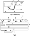
- Figure 1 illustrates at least a part of a typical PCB 100 including two microchips 104, 106.
- the first microchip 104 is connected to the second microchip 106 through a metallic wire 108.
- the empty space on the PCB 100 may be covered with a metallic layer 112 which may help reduce radio frequency (RF) interference.
- RF radio frequency
- a high frequency signal needs to be transmitted from the first microchip 104 to the second microchip 106 and this transmission is effectuated using the connecting wire 108.
- An example of this communication may be a distribution of local oscillator (LO) signals.
- the PCB 100 may also include radiating elements 110 to enable a system assembled on the PCB 100 to communicate with external system or systems wirelessly.
- a device in one embodiment, includes a wire board including metallic wiring and a first microchip connected to the metallic wiring.
- the first microchip includes a first radiating element configured to operate a first frequency.
- the device further includes a second microchip connect to the metallic wiring.
- the second microchip includes a second radiating element configured to operate at the first frequency.
- a main radiating element is also included.
- the main radiating element is configured to operate at a second radio frequency.
- the first microchip and the second microchip are physically placed such that the first radiating element faces the second radiating element.
- a device in another embodiment, includes a first wire board including a first metallic wiring and a second wire board including a second metallic wiring.
- the second wire board is not connected to the first wire board using metallic wires.
- the first wire board includes a first microchip connected to the first metallic wiring and the first microchip includes a first radiating element configured to operate a first frequency.
- the second wire board includes a second microchip connect to the second metallic wiring and the second microchip includes a second radiating element configured to operate at the first frequency.
- the second wire board further includes a main radiating element that is configured to operate at a second radio frequency. The first wire board and the second wire board are physically placed such that the first radiating element faces the second radiating element.
- the first frequency is N times greater than the second frequency, where N is an integer.
- the value of N may be selected from 2 to 10. In some embodiments, the value of N may be predetermined based on tests to minimize an interference between a signal having the first frequency and a signal having the second frequency.
- the first microchip is not connected to the second microchip using a metallic wire.
- the first microchip is connected to the second microchip using a metallic wire for low frequency communication.
- the wire board has a top side and an underside and the underside faces an opposing direction and the main radiating element is located on the underside while the first microchip is located on the top side.
- the wire board has a top side and an underside and the underside faces an opposing direction and wherein the main radiating element are located on the top side a connector array on the underside.
- the second microchip includes a third radiating element that is placed and configured to communicate with the main radiating element through a hole in the wire board.
- Figure 2 illustrates a cross section of a part of a printed circuit board or wiring board 202 of a device 200.
- the PCB 202 may be a multilayer structure having layers of conducting material isolated by non-conducting material. Toward the top, the PCB 202 may be at least partially covered by a material that helps reduce interference in a radio frequency (RF) communication.
- RF radio frequency
- a first microchip 204 and a second microchip 206 are shown to be connected to the conducting wiring through bond wires, interconnects or solder balls 214.
- the first microchip 204 and the second microchip 206 are shown to be Wafer Level Chip Scale Packaging (WLCSP) or Embedded Wafer Level Ball (eWLB) packaging. However, in other embodiments, conventional microchips with a plurality of pins may also be used.
- the first microchip 204 including a first radiating element 208 and the second microchip 206 includes a second radiating element 210.
- a radiating element is a small antenna that can transmit and receive radio signals.
- the first microchip 204 and the second microchip 206 include signal transmitters and receivers coupled to the radiating elements 208 and 210 respectively.
- the first microchip 204 may be connected to the second microchip 206 using a metallic wiring. If so connected, the wired connection is not used for high frequency transmission in the range greater than 500 megahertz, for example. In an embodiment, a wired connection is not used for a signal with a frequency at which a transmission through a wired connection causes an amount of parasitic radiation that interferes with the operations of the system 200 thus reducing the performance of the system 200. Instead, those high frequency signals are transmitted from the first microchip 204 to the second microchip 206 (or vice versa) wirelessly through the radiating elements 208, 210.
- the first microchip 204 and the second microchip 206 are oriented and placed on the PCB 202 such a way that the radiating elements 208, 210 align and there are no physical obstructions between them.
- the communication through the radiant elements 208, 210 may be used for local oscillator (LO) distribution for clock synchronizing the first microchip 204 and the second microchip 206.
- the frequency of the LO signal may be in the giga hertz range in applications such as radar sensors.
- a main radiating element or elements 212 may be fabricated using standard PCB manufacturing methods and the main radiating element 212 is used for transmitting or receiving signals from external devices.
- the radiating element 212 may be used for sensing radar signals if the device 200 is a radar sensor.
- the radiating elements 208, 210 may be of vivaldi antenna class or type.
- a Vivaldi antenna is a co-planar broadband-antenna, which may be made from a dielectric plate metalized on both sides.
- the radiating elements 208, 210 can be made for linear polarized waves or using two devices arranged in orthogonal direction for transmitting or receiving both polarization orientations.
- the radiating elements may be fed with 90-degree phase-shifted signals to transmit/receive circular-oriented electromagnetic waves.
- the PCB 202 may be double sided, that is, the PCB 202 includes active components on both sides. A use of double sided PCBs may help reduce overall device size.
- an array of connectors may be provided on the underside of the PCB 202. The connectors may be electrically connected to the top side of the PCB 202 through metallic interconnect fabricated through the thickness of the PCB 202.
- high frequency circuitry may be placed on one side and low frequency circuitry on the other side to reduce interference.
- a ball grid array 218 may be included on the underside of the PCB 202. The ball grid array 218 is designed to enable high density connections to be made more easily to integrated circuits by allowing the underside of a chip package to be used for the connectivity with other devices or systems.
- the carrier frequency at which the radiating elements 208, 210 operate may be in the whole positive multiples of the operating frequency of the main radiating element 212.
- the radiating elements 208, 210 may be configured to operate at the frequency N x f x , where N is an integer. Using a greater frequency cause no impact of the transmission pattern of the main radiating element 212. Further, the use of higher frequencies for the microchip to microchip communication does not cause spurious signals.
- Figure 3 shows a device 300 which employs a same or similar microchip to microchip commutation as described in Figure 2 .
- the device 300 includes a PCB 302 (or a section thereof) that includes a top side and an underside.
- the PCB 302 may be a multi-layered circuit board having multiple metallic layers isolated by non-conducting layers and having interconnects to selectively electrically connect metallic layers.
- a main radiating element 316 is incorporated on the underside. This arrangement effectively segregate radiating elements operating at different frequencies to reduce interference.
- the top side includes a microchip 308 that includes a first radiating element 312.
- the first microchip 308 is connected to other components (not shown) through solder balls or interconnect and a metallic layer of the top side of the PCB 302.
- the top side of the PCB 302 also includes a second microchip 306 that includes a second radiating element 314 that is oriented to provide communication with the first microchip 308.
- the second microchip 306 further includes a third radiating element 310 that is oriented to transmit signals towards the underside of the PCB 302.
- a hole is formed in the PCB 302 through its entire width.
- the second microchip 306 is placed on the top side such that the third radiating element 310 is located directly above the hole.
- the hole is covered either fully or partially by the main radiating element 316.
- another microchip with a radiating element may be placed on the hole on the underside.
- This microchip can receive signals from the third radiating element 310 transmit the received signals externally using the main radiating element 316.
- a microchip to main radiating element communication is also wireless.
- the size of the main radiating element 316 may depend of its operating frequency. Lower operating frequencies may require larger radiating elements. Therefore, having the main radiating element on the underside may provide greater design choices and compact devices operating at different frequencies because the underside may provide greater surface area for fabricating a bigger main radiating element 316.
- Figure 4 depicts the device 300 of Figure 3 in a different embodiment in which the first microchip 308 and the second microchip 306 are configured to communicate both wirelessly, as described above, as well as using a metallic wire 318. As described above, high frequency communication may be effectuated wirelessly and other communication may be performed through the metallic wire 318.
- Figure 5 discloses the device 400 that includes two separate PCBs, a first PCB 402 and a second PCB 410.
- the PCB 402 and the PCB 410 may not be connected to each other using any metallic wiring.
- the first PCB 402 includes a microchip 408 and the second PCB 410 includes a second microchip 406.
- the first microchip 408 includes a first radiating element and similarly the second microchip 406 includes a second radiating element.
- the PCB 402 and the PCB 410 may be oriented such that the first radiating element and the second radiating element faces each other and configured to transmit and receive signals.
- This embodiment provides a greater device design flexibility and is advantageous because the subsystems fabricated on both PCBs may be designed and manufactured separately and then may be easily assembled to form the device 400.
- This embodiment may be employed in radar application.
- the distance between the first radiating element and the second radiating element be in tens of multiples of the wavelength of the operating frequency of the two radiating elements.
Landscapes
- Engineering & Computer Science (AREA)
- Microelectronics & Electronic Packaging (AREA)
- Computer Networks & Wireless Communication (AREA)
- Signal Processing (AREA)
- Transceivers (AREA)
- Variable-Direction Aerials And Aerial Arrays (AREA)
Abstract
Description
- High frequency (HF) electromagnetic wave emitting or receiving devices may be provided in form of one or more integrated circuits. The integrated circuits may be arranged on a wiring board, e.g., a printed circuit board (PCB). An emission or a reception antenna that is suitably coupled to the integrated circuits may be arranged on the wiring board or be integrated therein. The wiring board may comprise one or more conductive layers and one or more isolating layers arranged atop each other in an alternating manner so that there is an isolating layer between each pair of adjacent conductive layers. Various electronic components such as conductors, capacitors, inductors, or microstrip lines may be integrated in the conductive layers.
-
Figure 1 illustrates at least a part of atypical PCB 100 including twomicrochips first microchip 104 is connected to thesecond microchip 106 through ametallic wire 108. The empty space on thePCB 100 may be covered with ametallic layer 112 which may help reduce radio frequency (RF) interference. In some applications, a high frequency signal needs to be transmitted from thefirst microchip 104 to thesecond microchip 106 and this transmission is effectuated using the connectingwire 108. An example of this communication may be a distribution of local oscillator (LO) signals. The PCB 100 may also includeradiating elements 110 to enable a system assembled on the PCB 100 to communicate with external system or systems wirelessly. - This Summary is provided to introduce a selection of concepts in a simplified form that are further described below in the Detailed Description. This Summary is not intended to identify key features or essential features of the claimed subject matter, nor is it intended to be used to limit the scope of the claimed subject matter.
- In one embodiment a device is disclosed. The device includes a wire board including metallic wiring and a first microchip connected to the metallic wiring. The first microchip includes a first radiating element configured to operate a first frequency. The device further includes a second microchip connect to the metallic wiring. The second microchip includes a second radiating element configured to operate at the first frequency. A main radiating element is also included. The main radiating element is configured to operate at a second radio frequency. The first microchip and the second microchip are physically placed such that the first radiating element faces the second radiating element.
- In another embodiment, a device is disclosed that includes a first wire board including a first metallic wiring and a second wire board including a second metallic wiring. The second wire board is not connected to the first wire board using metallic wires. The first wire board includes a first microchip connected to the first metallic wiring and the first microchip includes a first radiating element configured to operate a first frequency. The second wire board includes a second microchip connect to the second metallic wiring and the second microchip includes a second radiating element configured to operate at the first frequency. The second wire board further includes a main radiating element that is configured to operate at a second radio frequency. The first wire board and the second wire board are physically placed such that the first radiating element faces the second radiating element.
- In some embodiments, there is no physical obstacle between the first radiating element and the second radiating element and the first frequency is higher than the second frequency. The first frequency is N times greater than the second frequency, where N is an integer. The value of N may be selected from 2 to 10. In some embodiments, the value of N may be predetermined based on tests to minimize an interference between a signal having the first frequency and a signal having the second frequency.
- In some embodiments, the first microchip is not connected to the second microchip using a metallic wire. However, in some other embodiments, the first microchip is connected to the second microchip using a metallic wire for low frequency communication. The wire board has a top side and an underside and the underside faces an opposing direction and the main radiating element is located on the underside while the first microchip is located on the top side.
- In some other embodiments, the wire board has a top side and an underside and the underside faces an opposing direction and wherein the main radiating element are located on the top side a connector array on the underside. The second microchip includes a third radiating element that is placed and configured to communicate with the main radiating element through a hole in the wire board.
- So that the manner in which the above recited features of the present invention can be understood in detail, a more particular description of the invention, briefly summarized above, may be had by reference to embodiments, some of which are illustrated in the appended drawings. It is to be noted, however, that the appended drawings illustrate only typical embodiments of this invention and are therefore not to be considered limiting of its scope, for the invention may admit to other equally effective embodiments. Advantages of the subject matter claimed will become apparent to those skilled in the art upon reading this description in conjunction with the accompanying drawings, in which like reference numerals have been used to designate like elements, and in which:
-
FIG. 1 shows a layout of a typical printed circuit board (PCB) or wiring board; and -
FIGS. 2 and5 depict, in various embodiments, a cross section of a PCB including microchips with radiating elements and arranged on the PCB to communicate with each other wirelessly in accordance with one or more embodiments of the present disclosure. - Note that figures are not drawn to scale. Intermediate steps between figure transitions have been omitted so as not to obfuscate the disclosure. Those intermediate steps are known to a person skilled in the art.
- Many well-known manufacturing steps, components, and connectors have been omitted or not described in details in the description so as not to obfuscate the present disclosure.
-
Figure 2 illustrates a cross section of a part of a printed circuit board orwiring board 202 of adevice 200. The PCB 202 may be a multilayer structure having layers of conducting material isolated by non-conducting material. Toward the top, thePCB 202 may be at least partially covered by a material that helps reduce interference in a radio frequency (RF) communication. On the top surface of the PCB 202, there may be conducting wirings to interconnect microchips and other electronic components. Afirst microchip 204 and asecond microchip 206 are shown to be connected to the conducting wiring through bond wires, interconnects orsolder balls 214. Thefirst microchip 204 and thesecond microchip 206 are shown to be Wafer Level Chip Scale Packaging (WLCSP) or Embedded Wafer Level Ball (eWLB) packaging. However, in other embodiments, conventional microchips with a plurality of pins may also be used. Thefirst microchip 204 including a first radiatingelement 208 and thesecond microchip 206 includes a second radiatingelement 210. A radiating element is a small antenna that can transmit and receive radio signals. Thefirst microchip 204 and thesecond microchip 206 include signal transmitters and receivers coupled to theradiating elements - Additionally, in some embodiments, the
first microchip 204 may be connected to thesecond microchip 206 using a metallic wiring. If so connected, the wired connection is not used for high frequency transmission in the range greater than 500 megahertz, for example. In an embodiment, a wired connection is not used for a signal with a frequency at which a transmission through a wired connection causes an amount of parasitic radiation that interferes with the operations of thesystem 200 thus reducing the performance of thesystem 200. Instead, those high frequency signals are transmitted from thefirst microchip 204 to the second microchip 206 (or vice versa) wirelessly through theradiating elements first microchip 204 and thesecond microchip 206 are oriented and placed on thePCB 202 such a way that theradiating elements radiant elements first microchip 204 and thesecond microchip 206. In some embodiments, the frequency of the LO signal may be in the giga hertz range in applications such as radar sensors. A main radiating element orelements 212 may be fabricated using standard PCB manufacturing methods and themain radiating element 212 is used for transmitting or receiving signals from external devices. For example, the radiatingelement 212 may be used for sensing radar signals if thedevice 200 is a radar sensor. A person skilled in the art, however, would appreciate that the embodiments described herein may be used in other high frequency applications. - In some embodiments, the radiating
elements elements - In some embodiments, the
PCB 202 may be double sided, that is, thePCB 202 includes active components on both sides. A use of double sided PCBs may help reduce overall device size. Alternatively, an array of connectors may be provided on the underside of thePCB 202. The connectors may be electrically connected to the top side of thePCB 202 through metallic interconnect fabricated through the thickness of thePCB 202. In some embodiments, high frequency circuitry may be placed on one side and low frequency circuitry on the other side to reduce interference. In one embodiment, aball grid array 218 may be included on the underside of thePCB 202. Theball grid array 218 is designed to enable high density connections to be made more easily to integrated circuits by allowing the underside of a chip package to be used for the connectivity with other devices or systems. - It may be noted that the carrier frequency at which the radiating
elements main radiating element 212. Hence, if themain radiating element 212 operates at the frequency fx then the radiatingelements main radiating element 212. Further, the use of higher frequencies for the microchip to microchip communication does not cause spurious signals. -
Figure 3 shows adevice 300 which employs a same or similar microchip to microchip commutation as described inFigure 2 . As depicted, thedevice 300 includes a PCB 302 (or a section thereof) that includes a top side and an underside. ThePCB 302 may be a multi-layered circuit board having multiple metallic layers isolated by non-conducting layers and having interconnects to selectively electrically connect metallic layers. In this embodiment, amain radiating element 316 is incorporated on the underside. This arrangement effectively segregate radiating elements operating at different frequencies to reduce interference. The top side includes amicrochip 308 that includes afirst radiating element 312. Thefirst microchip 308 is connected to other components (not shown) through solder balls or interconnect and a metallic layer of the top side of thePCB 302. - The top side of the
PCB 302 also includes asecond microchip 306 that includes asecond radiating element 314 that is oriented to provide communication with thefirst microchip 308. Thesecond microchip 306 further includes athird radiating element 310 that is oriented to transmit signals towards the underside of thePCB 302. A hole is formed in thePCB 302 through its entire width. Thesecond microchip 306 is placed on the top side such that thethird radiating element 310 is located directly above the hole. In one embodiment, on the underside the hole is covered either fully or partially by themain radiating element 316. In another embodiment, another microchip with a radiating element may be placed on the hole on the underside. This microchip can receive signals from thethird radiating element 310 transmit the received signals externally using themain radiating element 316. Contrary to the embodiment ofFigure 2 in which thesecond microchip 206 is connected to themain radiating element 212 through a wire, in this embodiment, a microchip to main radiating element communication is also wireless. The size of themain radiating element 316 may depend of its operating frequency. Lower operating frequencies may require larger radiating elements. Therefore, having the main radiating element on the underside may provide greater design choices and compact devices operating at different frequencies because the underside may provide greater surface area for fabricating a biggermain radiating element 316. -
Figure 4 depicts thedevice 300 ofFigure 3 in a different embodiment in which thefirst microchip 308 and thesecond microchip 306 are configured to communicate both wirelessly, as described above, as well as using ametallic wire 318. As described above, high frequency communication may be effectuated wirelessly and other communication may be performed through themetallic wire 318. -
Figure 5 discloses thedevice 400 that includes two separate PCBs, afirst PCB 402 and asecond PCB 410. ThePCB 402 and thePCB 410 may not be connected to each other using any metallic wiring. Thefirst PCB 402 includes amicrochip 408 and thesecond PCB 410 includes asecond microchip 406. Thefirst microchip 408 includes a first radiating element and similarly thesecond microchip 406 includes a second radiating element. In thedevice 400, thePCB 402 and thePCB 410 may be oriented such that the first radiating element and the second radiating element faces each other and configured to transmit and receive signals. This embodiment provides a greater device design flexibility and is advantageous because the subsystems fabricated on both PCBs may be designed and manufactured separately and then may be easily assembled to form thedevice 400. This embodiment may be employed in radar application. The distance between the first radiating element and the second radiating element be in tens of multiples of the wavelength of the operating frequency of the two radiating elements. - Since the embodiments described herein do not use an
interconnect 108 such as shown inFigure 1 , more compact devices can be designed because of a relative of ease of placement of themicrochips PCB 202. - Some or all of these embodiments may be combined, some may be omitted altogether, and additional process steps can be added while still achieving the products described herein. Thus, the subject matter described herein can be embodied in many different variations, and all such variations are contemplated to be within the scope of what is claimed.
- While one or more implementations have been described by way of example and in terms of the specific embodiments, it is to be understood that one or more implementations are not limited to the disclosed embodiments. To the contrary, it is intended to cover various modifications and similar arrangements as would be apparent to those skilled in the art. Therefore, the scope of the appended claims should be accorded the broadest interpretation so as to encompass all such modifications and similar arrangements.
- The use of the terms "a" and "an" and "the" and similar referents in the context of describing the subject matter (particularly in the context of the following claims) are to be construed to cover both the singular and the plural, unless otherwise indicated herein or clearly contradicted by context. Recitation of ranges of values herein are merely intended to serve as a shorthand method of referring individually to each separate value falling within the range, unless otherwise indicated herein, and each separate value is incorporated into the specification as if it were individually recited herein. Furthermore, the foregoing description is for the purpose of illustration only, and not for the purpose of limitation, as the scope of protection sought is defined by the claims as set forth hereinafter together with any equivalents thereof entitled to. The use of any and all examples, or exemplary language (e.g., "such as") provided herein, is intended merely to better illustrate the subject matter and does not pose a limitation on the scope of the subject matter unless otherwise claimed. The use of the term "based on" and other like phrases indicating a condition for bringing about a result, both in the claims and in the written description, is not intended to foreclose any other conditions that bring about that result. No language in the specification should be construed as indicating any non-claimed element as essential to the practice of the invention as claimed.
- Preferred embodiments are described herein, including the best mode known to the inventor for carrying out the claimed subject matter. Of course, variations of those preferred embodiments will become apparent to those of ordinary skill in the art upon reading the foregoing description. The inventor expects skilled artisans to employ such variations as appropriate, and the inventor intends for the claimed subject matter to be practiced otherwise than as specifically described herein. Accordingly, this claimed subject matter includes all modifications and equivalents of the subject matter recited in the claims appended hereto as permitted by applicable law. Moreover, any combination of the above-described elements in all possible variations thereof is encompassed unless otherwise indicated herein or otherwise clearly contradicted by context.
Claims (15)
- A device, comprising:a wire board (202, 302) including metallic wiring;a first microchip (204, 308) connected to the metallic wiring, wherein the first microchip (204, 308) includes a first radiating element (208, 312) configured to operate a first frequency;a second microchip (206, 306) connect to the metallic wiring, wherein the second microchip (206, 306) includes a second radiating element (210, 314) configured to operate at the first frequency;a main radiating element (212, 316) that is configured to operate at a second radio frequency,wherein the first microchip (204, 308) and the second microchip (206, 306) are physically placed such that the first radiating element (208, 312) faces the second radiating element (210, 314).
- The device of claim 1, wherein there is no physical obstacle between the first radiating element (208, 312) and the second radiating element (210, 314).
- The device of claim 1 or claim 2, wherein the first frequency is higher than the second frequency.
- The device of any one of the claims 1 to 3, wherein the first frequency is N times greater than the second frequency, where N is an integer.
- The device of claim 4, wherein a value of N may be predetermined based on tests to minimize an interference between a signal having the first frequency and a signal having the second frequency.
- The device of any one of the claims 1 to 5, wherein the first microchip (204, 308) is not connected to the second microchip (206, 306) using a metallic wire.
- The device of any one of the claims 1 to 5, wherein the first microchip (204, 308) is connected to the second microchip (206, 306) using a metallic wire (318) for low frequency communication.
- The device of any one of the claims 1 to 7, wherein the wire board (202, 302) have a top side and an underside,wherein the underside faces an opposing direction and wherein the main radiating element (212, 316) is located on the underside while the first microchip (204, 308) is located on the top side; orwherein the main radiating element (212, 316) are located on the top side.
- The device of claim 8, wherein the second microchip (206, 306) includes a third radiating element (310) that is placed and configured to communicate with the main radiating element (212, 316) through a hole through thickness of the wire board (202, 302).
- The device of claim 9, wherein the wire board (202, 302) includes a connector array on the underside.
- A device, comprising:a first wire board (402) including a first metallic wiring;a second wire board (410) including a second metallic wiring, wherein the second wire board (410) is not connected to the first wire board (402) using metallic wires;wherein, the first wire board (402) includes a first microchip (408) connected to the first metallic wiring, wherein the first microchip (408) includes a first radiating element configured to operate a first frequency;wherein the second wire board (410) includes a second microchip (406) connect to the second metallic wiring, wherein the second microchip includes a second radiating element configured to operate at the first frequency, wherein the second wire board (410) further includes a main radiating element that is configured to operate at a second radio frequency,wherein the first wire board (402) and the second wire board (410) are physically placed such that the first radiating element faces the second radiating element.
- The device of claim 11, wherein there is no physical obstacle between the first radiating element and the second radiating element.
- The device of claim 11 or claim 12, wherein the first frequency is higher than the second frequency.
- The device of any one of the claims 11 to 13, wherein the first frequency is N times greater than the second frequency, where N is an integer.
- The device of claim 14, wherein a value of N may be predetermined based on tests to minimize an interference between a signal having the first frequency and a signal having the second frequency.
Applications Claiming Priority (1)
| Application Number | Priority Date | Filing Date | Title |
|---|---|---|---|
| US15/597,532 US10516207B2 (en) | 2017-05-17 | 2017-05-17 | High frequency system, communication link |
Publications (2)
| Publication Number | Publication Date |
|---|---|
| EP3404767A1 true EP3404767A1 (en) | 2018-11-21 |
| EP3404767B1 EP3404767B1 (en) | 2021-06-09 |
Family
ID=61911432
Family Applications (1)
| Application Number | Title | Priority Date | Filing Date |
|---|---|---|---|
| EP18165924.4A Active EP3404767B1 (en) | 2017-05-17 | 2018-04-05 | High frequency system, communication link |
Country Status (3)
| Country | Link |
|---|---|
| US (1) | US10516207B2 (en) |
| EP (1) | EP3404767B1 (en) |
| CN (1) | CN108966480B (en) |
Families Citing this family (1)
| Publication number | Priority date | Publication date | Assignee | Title |
|---|---|---|---|---|
| CN116826368A (en) * | 2023-07-25 | 2023-09-29 | 加特兰微电子科技(上海)有限公司 | An antenna system, radar sensor system and electronic device |
Citations (2)
| Publication number | Priority date | Publication date | Assignee | Title |
|---|---|---|---|---|
| US20080293446A1 (en) * | 2007-05-23 | 2008-11-27 | Broadcom Corporation | Fully integrated RF transceiver integrated circuit |
| US20120263244A1 (en) * | 2011-03-24 | 2012-10-18 | Waveconnex, Inc. | Integrated circuit with electromagnetic communication |
Family Cites Families (33)
| Publication number | Priority date | Publication date | Assignee | Title |
|---|---|---|---|---|
| JPS5728401A (en) | 1980-07-29 | 1982-02-16 | Nec Corp | Waveguide spacer and its manufacture |
| JP2743391B2 (en) | 1988-08-25 | 1998-04-22 | ソニー株式会社 | Method for manufacturing semiconductor memory |
| US6154176A (en) | 1998-08-07 | 2000-11-28 | Sarnoff Corporation | Antennas formed using multilayer ceramic substrates |
| US6713685B1 (en) | 1998-09-10 | 2004-03-30 | Viasystems Group, Inc. | Non-circular micro-via |
| WO2000016443A1 (en) | 1998-09-10 | 2000-03-23 | Viasystems Group, Inc. | Non-circular micro-via |
| US6297551B1 (en) | 1999-09-22 | 2001-10-02 | Agere Systems Guardian Corp. | Integrated circuit packages with improved EMI characteristics |
| US20040018599A1 (en) | 2002-07-24 | 2004-01-29 | Rabinowitz Israel N. | Enhanced production from almond hulls of products such as inositol and inositol phosphates |
| US7126542B2 (en) | 2002-11-19 | 2006-10-24 | Farrokh Mohamadi | Integrated antenna module with micro-waveguide |
| JP2006217047A (en) * | 2005-02-01 | 2006-08-17 | Chant Sincere Co Ltd | Method for manufacturing microchip antenna |
| EP1949491B1 (en) | 2005-11-14 | 2011-07-06 | VEGA Grieshaber KG | Waveguide junction |
| US8478344B2 (en) * | 2006-06-21 | 2013-07-02 | Broadcom Corporation | Power recovery circuit based on partial standing waves |
| US8032089B2 (en) * | 2006-12-30 | 2011-10-04 | Broadcom Corporation | Integrated circuit/printed circuit board substrate structure and communications |
| US7974587B2 (en) * | 2006-12-30 | 2011-07-05 | Broadcom Corporation | Local wireless communications within a device |
| US8289944B2 (en) | 2007-01-31 | 2012-10-16 | Broadcom Corporation | Apparatus for configuration of wireless operation |
| US8116294B2 (en) * | 2007-01-31 | 2012-02-14 | Broadcom Corporation | RF bus controller |
| WO2008129923A1 (en) | 2007-04-13 | 2008-10-30 | Kyocera Corporation | High frequency circuit board, high frequency circuit module, and radar device |
| US7952531B2 (en) | 2007-07-13 | 2011-05-31 | International Business Machines Corporation | Planar circularly polarized antennas |
| US7908420B2 (en) * | 2007-07-31 | 2011-03-15 | Broadcom Corporation | Processing system with millimeter wave host interface and method for use therewith |
| WO2009041696A1 (en) | 2007-09-27 | 2009-04-02 | Kyocera Corporation | High frequency module and wiring board |
| US7579997B2 (en) | 2007-10-03 | 2009-08-25 | The Boeing Company | Advanced antenna integrated printed wiring board with metallic waveguide plate |
| JP4827825B2 (en) | 2007-12-03 | 2011-11-30 | 日立オートモティブシステムズ株式会社 | High frequency module |
| US8278749B2 (en) | 2009-01-30 | 2012-10-02 | Infineon Technologies Ag | Integrated antennas in wafer level package |
| US7977785B2 (en) | 2009-03-05 | 2011-07-12 | Freescale Semiconductor, Inc. | Electronic device including dies, a dielectric layer, and a encapsulating layer |
| DE112010001453B4 (en) | 2009-03-31 | 2017-06-22 | Kyocera Corp. | Circuit board, waveguide structure, high frequency module and radar device |
| KR101038236B1 (en) * | 2009-09-16 | 2011-06-01 | 삼성전기주식회사 | printed circuit board having electromagnetic bandgap structure |
| JP5375719B2 (en) * | 2010-04-01 | 2013-12-25 | Tdk株式会社 | ANTENNA DEVICE AND RADIO COMMUNICATION DEVICE USING THE SAME |
| US8451618B2 (en) | 2010-10-28 | 2013-05-28 | Infineon Technologies Ag | Integrated antennas in wafer level package |
| JP5724538B2 (en) | 2011-03-31 | 2015-05-27 | ソニー株式会社 | Signal transmission device, communication device, electronic device, and signal transmission method |
| KR101796341B1 (en) * | 2011-05-12 | 2017-11-10 | 키사, 아이엔씨. | Scalable high-bandwidth connectivity |
| EP2832192B1 (en) * | 2012-03-28 | 2017-09-27 | Keyssa, Inc. | Redirection of electromagnetic signals using substrate structures |
| WO2014108744A1 (en) * | 2013-01-09 | 2014-07-17 | Freescale Semiconductor, Inc. | Electronic high frequency device and manufacturing method |
| EP2860757B1 (en) * | 2013-09-11 | 2019-12-11 | Nxp B.V. | Integrated circuit |
| US9887449B2 (en) * | 2014-08-29 | 2018-02-06 | Nxp Usa, Inc. | Radio frequency coupling structure and a method of manufacturing thereof |
-
2017
- 2017-05-17 US US15/597,532 patent/US10516207B2/en active Active
-
2018
- 2018-04-05 EP EP18165924.4A patent/EP3404767B1/en active Active
- 2018-05-17 CN CN201810476780.5A patent/CN108966480B/en active Active
Patent Citations (2)
| Publication number | Priority date | Publication date | Assignee | Title |
|---|---|---|---|---|
| US20080293446A1 (en) * | 2007-05-23 | 2008-11-27 | Broadcom Corporation | Fully integrated RF transceiver integrated circuit |
| US20120263244A1 (en) * | 2011-03-24 | 2012-10-18 | Waveconnex, Inc. | Integrated circuit with electromagnetic communication |
Also Published As
| Publication number | Publication date |
|---|---|
| US20180337448A1 (en) | 2018-11-22 |
| EP3404767B1 (en) | 2021-06-09 |
| US10516207B2 (en) | 2019-12-24 |
| CN108966480B (en) | 2023-01-10 |
| CN108966480A (en) | 2018-12-07 |
Similar Documents
| Publication | Publication Date | Title |
|---|---|---|
| KR102099578B1 (en) | Radio frequency device packages and methods of formation thereof | |
| US7764235B2 (en) | Semiconductor device | |
| US8089107B2 (en) | Three-dimensional integrated device | |
| US9705204B2 (en) | Low-profile wireless connectors | |
| US8917218B2 (en) | Circuit board and circuit module | |
| US11715886B2 (en) | Low-cost, IPD and laminate based antenna array module | |
| EP3041087B1 (en) | Wireless communication device | |
| US9698482B2 (en) | Antenna device | |
| CN110506367A (en) | Anneta module and communication device | |
| CN105703066A (en) | Switchable transmit and receive phased array antenna | |
| KR102414981B1 (en) | Radio-frequency module | |
| CN104145335B (en) | Semiconductor module with integrated antenna structure | |
| KR20080106354A (en) | Antenna device and RF communication equipment | |
| US20230411870A1 (en) | Antenna module and communication apparatus equipped with the same | |
| JP2016502262A (en) | Electronic devices and land grid array modules | |
| US10516207B2 (en) | High frequency system, communication link | |
| US7352056B2 (en) | Semiconductor package structure with microstrip antennan | |
| US20110109521A1 (en) | Electronic device comprising a semiconductor component integrating an antenna | |
| CN107180819B (en) | Signal isolation structure for electromagnetic communication | |
| US20050167797A1 (en) | Structure package | |
| US10505276B2 (en) | Wireless communications assembly with integrated active phased-array antenna | |
| US20240047853A1 (en) | Antenna module | |
| EP3755127A1 (en) | A printed circuit board (pcb) module comprising an embedded radiofrequency semiconductor die | |
| US10454526B1 (en) | Structures for cross-talk reduction | |
| JP2006319867A (en) | Antenna module and wireless device using the same |
Legal Events
| Date | Code | Title | Description |
|---|---|---|---|
| PUAI | Public reference made under article 153(3) epc to a published international application that has entered the european phase |
Free format text: ORIGINAL CODE: 0009012 |
|
| STAA | Information on the status of an ep patent application or granted ep patent |
Free format text: STATUS: THE APPLICATION HAS BEEN PUBLISHED |
|
| AK | Designated contracting states |
Kind code of ref document: A1 Designated state(s): AL AT BE BG CH CY CZ DE DK EE ES FI FR GB GR HR HU IE IS IT LI LT LU LV MC MK MT NL NO PL PT RO RS SE SI SK SM TR |
|
| AX | Request for extension of the european patent |
Extension state: BA ME |
|
| STAA | Information on the status of an ep patent application or granted ep patent |
Free format text: STATUS: REQUEST FOR EXAMINATION WAS MADE |
|
| 17P | Request for examination filed |
Effective date: 20190521 |
|
| RBV | Designated contracting states (corrected) |
Designated state(s): AL AT BE BG CH CY CZ DE DK EE ES FI FR GB GR HR HU IE IS IT LI LT LU LV MC MK MT NL NO PL PT RO RS SE SI SK SM TR |
|
| STAA | Information on the status of an ep patent application or granted ep patent |
Free format text: STATUS: EXAMINATION IS IN PROGRESS |
|
| 17Q | First examination report despatched |
Effective date: 20200414 |
|
| GRAP | Despatch of communication of intention to grant a patent |
Free format text: ORIGINAL CODE: EPIDOSNIGR1 |
|
| STAA | Information on the status of an ep patent application or granted ep patent |
Free format text: STATUS: GRANT OF PATENT IS INTENDED |
|
| INTG | Intention to grant announced |
Effective date: 20201215 |
|
| GRAJ | Information related to disapproval of communication of intention to grant by the applicant or resumption of examination proceedings by the epo deleted |
Free format text: ORIGINAL CODE: EPIDOSDIGR1 |
|
| STAA | Information on the status of an ep patent application or granted ep patent |
Free format text: STATUS: EXAMINATION IS IN PROGRESS |
|
| INTC | Intention to grant announced (deleted) | ||
| GRAP | Despatch of communication of intention to grant a patent |
Free format text: ORIGINAL CODE: EPIDOSNIGR1 |
|
| STAA | Information on the status of an ep patent application or granted ep patent |
Free format text: STATUS: GRANT OF PATENT IS INTENDED |
|
| GRAS | Grant fee paid |
Free format text: ORIGINAL CODE: EPIDOSNIGR3 |
|
| GRAA | (expected) grant |
Free format text: ORIGINAL CODE: 0009210 |
|
| STAA | Information on the status of an ep patent application or granted ep patent |
Free format text: STATUS: THE PATENT HAS BEEN GRANTED |
|
| INTG | Intention to grant announced |
Effective date: 20210414 |
|
| AK | Designated contracting states |
Kind code of ref document: B1 Designated state(s): AL AT BE BG CH CY CZ DE DK EE ES FI FR GB GR HR HU IE IS IT LI LT LU LV MC MK MT NL NO PL PT RO RS SE SI SK SM TR |
|
| REG | Reference to a national code |
Ref country code: GB Ref legal event code: FG4D |
|
| REG | Reference to a national code |
Ref country code: CH Ref legal event code: EP Ref country code: AT Ref legal event code: REF Ref document number: 1401237 Country of ref document: AT Kind code of ref document: T Effective date: 20210615 |
|
| REG | Reference to a national code |
Ref country code: DE Ref legal event code: R096 Ref document number: 602018018232 Country of ref document: DE |
|
| REG | Reference to a national code |
Ref country code: IE Ref legal event code: FG4D |
|
| REG | Reference to a national code |
Ref country code: LT Ref legal event code: MG9D |
|
| PG25 | Lapsed in a contracting state [announced via postgrant information from national office to epo] |
Ref country code: FI Free format text: LAPSE BECAUSE OF FAILURE TO SUBMIT A TRANSLATION OF THE DESCRIPTION OR TO PAY THE FEE WITHIN THE PRESCRIBED TIME-LIMIT Effective date: 20210609 Ref country code: LT Free format text: LAPSE BECAUSE OF FAILURE TO SUBMIT A TRANSLATION OF THE DESCRIPTION OR TO PAY THE FEE WITHIN THE PRESCRIBED TIME-LIMIT Effective date: 20210609 Ref country code: HR Free format text: LAPSE BECAUSE OF FAILURE TO SUBMIT A TRANSLATION OF THE DESCRIPTION OR TO PAY THE FEE WITHIN THE PRESCRIBED TIME-LIMIT Effective date: 20210609 Ref country code: BG Free format text: LAPSE BECAUSE OF FAILURE TO SUBMIT A TRANSLATION OF THE DESCRIPTION OR TO PAY THE FEE WITHIN THE PRESCRIBED TIME-LIMIT Effective date: 20210909 |
|
| REG | Reference to a national code |
Ref country code: AT Ref legal event code: MK05 Ref document number: 1401237 Country of ref document: AT Kind code of ref document: T Effective date: 20210609 |
|
| REG | Reference to a national code |
Ref country code: NL Ref legal event code: MP Effective date: 20210609 |
|
| PG25 | Lapsed in a contracting state [announced via postgrant information from national office to epo] |
Ref country code: GR Free format text: LAPSE BECAUSE OF FAILURE TO SUBMIT A TRANSLATION OF THE DESCRIPTION OR TO PAY THE FEE WITHIN THE PRESCRIBED TIME-LIMIT Effective date: 20210910 Ref country code: SE Free format text: LAPSE BECAUSE OF FAILURE TO SUBMIT A TRANSLATION OF THE DESCRIPTION OR TO PAY THE FEE WITHIN THE PRESCRIBED TIME-LIMIT Effective date: 20210609 Ref country code: RS Free format text: LAPSE BECAUSE OF FAILURE TO SUBMIT A TRANSLATION OF THE DESCRIPTION OR TO PAY THE FEE WITHIN THE PRESCRIBED TIME-LIMIT Effective date: 20210609 Ref country code: LV Free format text: LAPSE BECAUSE OF FAILURE TO SUBMIT A TRANSLATION OF THE DESCRIPTION OR TO PAY THE FEE WITHIN THE PRESCRIBED TIME-LIMIT Effective date: 20210609 Ref country code: NO Free format text: LAPSE BECAUSE OF FAILURE TO SUBMIT A TRANSLATION OF THE DESCRIPTION OR TO PAY THE FEE WITHIN THE PRESCRIBED TIME-LIMIT Effective date: 20210909 |
|
| PG25 | Lapsed in a contracting state [announced via postgrant information from national office to epo] |
Ref country code: ES Free format text: LAPSE BECAUSE OF FAILURE TO SUBMIT A TRANSLATION OF THE DESCRIPTION OR TO PAY THE FEE WITHIN THE PRESCRIBED TIME-LIMIT Effective date: 20210609 Ref country code: EE Free format text: LAPSE BECAUSE OF FAILURE TO SUBMIT A TRANSLATION OF THE DESCRIPTION OR TO PAY THE FEE WITHIN THE PRESCRIBED TIME-LIMIT Effective date: 20210609 Ref country code: SK Free format text: LAPSE BECAUSE OF FAILURE TO SUBMIT A TRANSLATION OF THE DESCRIPTION OR TO PAY THE FEE WITHIN THE PRESCRIBED TIME-LIMIT Effective date: 20210609 Ref country code: SM Free format text: LAPSE BECAUSE OF FAILURE TO SUBMIT A TRANSLATION OF THE DESCRIPTION OR TO PAY THE FEE WITHIN THE PRESCRIBED TIME-LIMIT Effective date: 20210609 Ref country code: AT Free format text: LAPSE BECAUSE OF FAILURE TO SUBMIT A TRANSLATION OF THE DESCRIPTION OR TO PAY THE FEE WITHIN THE PRESCRIBED TIME-LIMIT Effective date: 20210609 Ref country code: CZ Free format text: LAPSE BECAUSE OF FAILURE TO SUBMIT A TRANSLATION OF THE DESCRIPTION OR TO PAY THE FEE WITHIN THE PRESCRIBED TIME-LIMIT Effective date: 20210609 Ref country code: NL Free format text: LAPSE BECAUSE OF FAILURE TO SUBMIT A TRANSLATION OF THE DESCRIPTION OR TO PAY THE FEE WITHIN THE PRESCRIBED TIME-LIMIT Effective date: 20210609 Ref country code: PT Free format text: LAPSE BECAUSE OF FAILURE TO SUBMIT A TRANSLATION OF THE DESCRIPTION OR TO PAY THE FEE WITHIN THE PRESCRIBED TIME-LIMIT Effective date: 20211011 Ref country code: RO Free format text: LAPSE BECAUSE OF FAILURE TO SUBMIT A TRANSLATION OF THE DESCRIPTION OR TO PAY THE FEE WITHIN THE PRESCRIBED TIME-LIMIT Effective date: 20210609 |
|
| PG25 | Lapsed in a contracting state [announced via postgrant information from national office to epo] |
Ref country code: PL Free format text: LAPSE BECAUSE OF FAILURE TO SUBMIT A TRANSLATION OF THE DESCRIPTION OR TO PAY THE FEE WITHIN THE PRESCRIBED TIME-LIMIT Effective date: 20210609 |
|
| REG | Reference to a national code |
Ref country code: DE Ref legal event code: R097 Ref document number: 602018018232 Country of ref document: DE |
|
| PLBE | No opposition filed within time limit |
Free format text: ORIGINAL CODE: 0009261 |
|
| STAA | Information on the status of an ep patent application or granted ep patent |
Free format text: STATUS: NO OPPOSITION FILED WITHIN TIME LIMIT |
|
| PG25 | Lapsed in a contracting state [announced via postgrant information from national office to epo] |
Ref country code: DK Free format text: LAPSE BECAUSE OF FAILURE TO SUBMIT A TRANSLATION OF THE DESCRIPTION OR TO PAY THE FEE WITHIN THE PRESCRIBED TIME-LIMIT Effective date: 20210609 |
|
| 26N | No opposition filed |
Effective date: 20220310 |
|
| PG25 | Lapsed in a contracting state [announced via postgrant information from national office to epo] |
Ref country code: AL Free format text: LAPSE BECAUSE OF FAILURE TO SUBMIT A TRANSLATION OF THE DESCRIPTION OR TO PAY THE FEE WITHIN THE PRESCRIBED TIME-LIMIT Effective date: 20210609 |
|
| PG25 | Lapsed in a contracting state [announced via postgrant information from national office to epo] |
Ref country code: IT Free format text: LAPSE BECAUSE OF FAILURE TO SUBMIT A TRANSLATION OF THE DESCRIPTION OR TO PAY THE FEE WITHIN THE PRESCRIBED TIME-LIMIT Effective date: 20210609 |
|
| REG | Reference to a national code |
Ref country code: CH Ref legal event code: PL |
|
| REG | Reference to a national code |
Ref country code: BE Ref legal event code: MM Effective date: 20220430 |
|
| PG25 | Lapsed in a contracting state [announced via postgrant information from national office to epo] |
Ref country code: MC Free format text: LAPSE BECAUSE OF FAILURE TO SUBMIT A TRANSLATION OF THE DESCRIPTION OR TO PAY THE FEE WITHIN THE PRESCRIBED TIME-LIMIT Effective date: 20210609 Ref country code: LU Free format text: LAPSE BECAUSE OF NON-PAYMENT OF DUE FEES Effective date: 20220405 Ref country code: LI Free format text: LAPSE BECAUSE OF NON-PAYMENT OF DUE FEES Effective date: 20220430 Ref country code: CH Free format text: LAPSE BECAUSE OF NON-PAYMENT OF DUE FEES Effective date: 20220430 |
|
| PG25 | Lapsed in a contracting state [announced via postgrant information from national office to epo] |
Ref country code: BE Free format text: LAPSE BECAUSE OF NON-PAYMENT OF DUE FEES Effective date: 20220430 |
|
| PG25 | Lapsed in a contracting state [announced via postgrant information from national office to epo] |
Ref country code: IE Free format text: LAPSE BECAUSE OF NON-PAYMENT OF DUE FEES Effective date: 20220405 |
|
| P01 | Opt-out of the competence of the unified patent court (upc) registered |
Effective date: 20230725 |
|
| PG25 | Lapsed in a contracting state [announced via postgrant information from national office to epo] |
Ref country code: HU Free format text: LAPSE BECAUSE OF FAILURE TO SUBMIT A TRANSLATION OF THE DESCRIPTION OR TO PAY THE FEE WITHIN THE PRESCRIBED TIME-LIMIT; INVALID AB INITIO Effective date: 20180405 |
|
| PG25 | Lapsed in a contracting state [announced via postgrant information from national office to epo] |
Ref country code: MK Free format text: LAPSE BECAUSE OF FAILURE TO SUBMIT A TRANSLATION OF THE DESCRIPTION OR TO PAY THE FEE WITHIN THE PRESCRIBED TIME-LIMIT Effective date: 20210609 Ref country code: CY Free format text: LAPSE BECAUSE OF FAILURE TO SUBMIT A TRANSLATION OF THE DESCRIPTION OR TO PAY THE FEE WITHIN THE PRESCRIBED TIME-LIMIT Effective date: 20210609 |
|
| PG25 | Lapsed in a contracting state [announced via postgrant information from national office to epo] |
Ref country code: MT Free format text: LAPSE BECAUSE OF FAILURE TO SUBMIT A TRANSLATION OF THE DESCRIPTION OR TO PAY THE FEE WITHIN THE PRESCRIBED TIME-LIMIT Effective date: 20210609 |
|
| PGFP | Annual fee paid to national office [announced via postgrant information from national office to epo] |
Ref country code: DE Payment date: 20250319 Year of fee payment: 8 |
|
| PG25 | Lapsed in a contracting state [announced via postgrant information from national office to epo] |
Ref country code: TR Free format text: LAPSE BECAUSE OF FAILURE TO SUBMIT A TRANSLATION OF THE DESCRIPTION OR TO PAY THE FEE WITHIN THE PRESCRIBED TIME-LIMIT Effective date: 20210609 |
|
| PGFP | Annual fee paid to national office [announced via postgrant information from national office to epo] |
Ref country code: GB Payment date: 20260319 Year of fee payment: 9 |
|
| PGFP | Annual fee paid to national office [announced via postgrant information from national office to epo] |
Ref country code: FR Payment date: 20260320 Year of fee payment: 9 |