EP3404507A1 - Double-threaded connector - Google Patents
Double-threaded connector Download PDFInfo
- Publication number
- EP3404507A1 EP3404507A1 EP18172980.7A EP18172980A EP3404507A1 EP 3404507 A1 EP3404507 A1 EP 3404507A1 EP 18172980 A EP18172980 A EP 18172980A EP 3404507 A1 EP3404507 A1 EP 3404507A1
- Authority
- EP
- European Patent Office
- Prior art keywords
- cylindrical
- outer body
- component
- double
- stage
- Prior art date
- Legal status (The legal status is an assumption and is not a legal conclusion. Google has not performed a legal analysis and makes no representation as to the accuracy of the status listed.)
- Granted
Links
Images


Classifications
-
- H—ELECTRICITY
- H01—ELECTRIC ELEMENTS
- H01R—ELECTRICALLY-CONDUCTIVE CONNECTIONS; STRUCTURAL ASSOCIATIONS OF A PLURALITY OF MUTUALLY-INSULATED ELECTRICAL CONNECTING ELEMENTS; COUPLING DEVICES; CURRENT COLLECTORS
- H01R12/00—Structural associations of a plurality of mutually-insulated electrical connecting elements, specially adapted for printed circuits, e.g. printed circuit boards [PCB], flat or ribbon cables, or like generally planar structures, e.g. terminal strips, terminal blocks; Coupling devices specially adapted for printed circuits, flat or ribbon cables, or like generally planar structures; Terminals specially adapted for contact with, or insertion into, printed circuits, flat or ribbon cables, or like generally planar structures
- H01R12/70—Coupling devices
- H01R12/71—Coupling devices for rigid printing circuits or like structures
- H01R12/72—Coupling devices for rigid printing circuits or like structures coupling with the edge of the rigid printed circuits or like structures
- H01R12/73—Coupling devices for rigid printing circuits or like structures coupling with the edge of the rigid printed circuits or like structures connecting to other rigid printed circuits or like structures
-
- H—ELECTRICITY
- H05—ELECTRIC TECHNIQUES NOT OTHERWISE PROVIDED FOR
- H05K—PRINTED CIRCUITS; CASINGS OR CONSTRUCTIONAL DETAILS OF ELECTRIC APPARATUS; MANUFACTURE OF ASSEMBLAGES OF ELECTRICAL COMPONENTS
- H05K1/00—Printed circuits
- H05K1/02—Details
- H05K1/14—Structural association of two or more printed circuits
- H05K1/141—One or more single auxiliary printed circuits mounted on a main printed circuit, e.g. modules, adapters
-
- F—MECHANICAL ENGINEERING; LIGHTING; HEATING; WEAPONS; BLASTING
- F16—ENGINEERING ELEMENTS AND UNITS; GENERAL MEASURES FOR PRODUCING AND MAINTAINING EFFECTIVE FUNCTIONING OF MACHINES OR INSTALLATIONS; THERMAL INSULATION IN GENERAL
- F16B—DEVICES FOR FASTENING OR SECURING CONSTRUCTIONAL ELEMENTS OR MACHINE PARTS TOGETHER, e.g. NAILS, BOLTS, CIRCLIPS, CLAMPS, CLIPS OR WEDGES; JOINTS OR JOINTING
- F16B37/00—Nuts or like thread-engaging members
- F16B37/12—Nuts or like thread-engaging members with thread-engaging surfaces formed by inserted coil-springs, discs, or the like; Independent pieces of wound wire used as nuts; Threaded inserts for holes
- F16B37/122—Threaded inserts, e.g. "rampa bolts"
- F16B37/125—Threaded inserts, e.g. "rampa bolts" the external surface of the insert being threaded
- F16B37/127—Threaded inserts, e.g. "rampa bolts" the external surface of the insert being threaded and self-tapping
-
- G—PHYSICS
- G06—COMPUTING OR CALCULATING; COUNTING
- G06F—ELECTRIC DIGITAL DATA PROCESSING
- G06F1/00—Details not covered by groups G06F3/00 - G06F13/00 and G06F21/00
- G06F1/16—Constructional details or arrangements
- G06F1/18—Packaging or power distribution
- G06F1/183—Internal mounting support structures, e.g. for supporting printed circuit boards
- G06F1/185—Mounting of expansion boards
-
- H—ELECTRICITY
- H01—ELECTRIC ELEMENTS
- H01R—ELECTRICALLY-CONDUCTIVE CONNECTIONS; STRUCTURAL ASSOCIATIONS OF A PLURALITY OF MUTUALLY-INSULATED ELECTRICAL CONNECTING ELEMENTS; COUPLING DEVICES; CURRENT COLLECTORS
- H01R12/00—Structural associations of a plurality of mutually-insulated electrical connecting elements, specially adapted for printed circuits, e.g. printed circuit boards [PCB], flat or ribbon cables, or like generally planar structures, e.g. terminal strips, terminal blocks; Coupling devices specially adapted for printed circuits, flat or ribbon cables, or like generally planar structures; Terminals specially adapted for contact with, or insertion into, printed circuits, flat or ribbon cables, or like generally planar structures
- H01R12/70—Coupling devices
- H01R12/71—Coupling devices for rigid printing circuits or like structures
- H01R12/72—Coupling devices for rigid printing circuits or like structures coupling with the edge of the rigid printed circuits or like structures
- H01R12/721—Coupling devices for rigid printing circuits or like structures coupling with the edge of the rigid printed circuits or like structures cooperating directly with the edge of the rigid printed circuits
-
- H—ELECTRICITY
- H05—ELECTRIC TECHNIQUES NOT OTHERWISE PROVIDED FOR
- H05K—PRINTED CIRCUITS; CASINGS OR CONSTRUCTIONAL DETAILS OF ELECTRIC APPARATUS; MANUFACTURE OF ASSEMBLAGES OF ELECTRICAL COMPONENTS
- H05K3/00—Apparatus or processes for manufacturing printed circuits
- H05K3/36—Assembling printed circuits with other printed circuits
- H05K3/368—Assembling printed circuits with other printed circuits parallel to each other
-
- H—ELECTRICITY
- H05—ELECTRIC TECHNIQUES NOT OTHERWISE PROVIDED FOR
- H05K—PRINTED CIRCUITS; CASINGS OR CONSTRUCTIONAL DETAILS OF ELECTRIC APPARATUS; MANUFACTURE OF ASSEMBLAGES OF ELECTRICAL COMPONENTS
- H05K7/00—Constructional details common to different types of electric apparatus
- H05K7/14—Mounting supporting structure in casing or on frame or rack
- H05K7/1417—Mounting supporting structure in casing or on frame or rack having securing means for mounting boards, plates or wiring boards
- H05K7/142—Spacers not being card guides
-
- F—MECHANICAL ENGINEERING; LIGHTING; HEATING; WEAPONS; BLASTING
- F16—ENGINEERING ELEMENTS AND UNITS; GENERAL MEASURES FOR PRODUCING AND MAINTAINING EFFECTIVE FUNCTIONING OF MACHINES OR INSTALLATIONS; THERMAL INSULATION IN GENERAL
- F16B—DEVICES FOR FASTENING OR SECURING CONSTRUCTIONAL ELEMENTS OR MACHINE PARTS TOGETHER, e.g. NAILS, BOLTS, CIRCLIPS, CLAMPS, CLIPS OR WEDGES; JOINTS OR JOINTING
- F16B2200/00—Constructional details of connections not covered for in other groups of this subclass
- F16B2200/93—Fastener comprising feature for establishing a good electrical connection, e.g. electrostatic discharge or insulation feature
-
- F—MECHANICAL ENGINEERING; LIGHTING; HEATING; WEAPONS; BLASTING
- F16—ENGINEERING ELEMENTS AND UNITS; GENERAL MEASURES FOR PRODUCING AND MAINTAINING EFFECTIVE FUNCTIONING OF MACHINES OR INSTALLATIONS; THERMAL INSULATION IN GENERAL
- F16B—DEVICES FOR FASTENING OR SECURING CONSTRUCTIONAL ELEMENTS OR MACHINE PARTS TOGETHER, e.g. NAILS, BOLTS, CIRCLIPS, CLAMPS, CLIPS OR WEDGES; JOINTS OR JOINTING
- F16B5/00—Joining sheets or plates, e.g. panels, to one another or to strips or bars parallel to them
- F16B5/02—Joining sheets or plates, e.g. panels, to one another or to strips or bars parallel to them by means of fastening members using screw-thread
- F16B5/0283—Joining sheets or plates, e.g. panels, to one another or to strips or bars parallel to them by means of fastening members using screw-thread with an externally threaded sleeve around the neck or the head of the screw-threaded element for adjustably fastening a plate or frame or the like to a fixed element
-
- F—MECHANICAL ENGINEERING; LIGHTING; HEATING; WEAPONS; BLASTING
- F16—ENGINEERING ELEMENTS AND UNITS; GENERAL MEASURES FOR PRODUCING AND MAINTAINING EFFECTIVE FUNCTIONING OF MACHINES OR INSTALLATIONS; THERMAL INSULATION IN GENERAL
- F16B—DEVICES FOR FASTENING OR SECURING CONSTRUCTIONAL ELEMENTS OR MACHINE PARTS TOGETHER, e.g. NAILS, BOLTS, CIRCLIPS, CLAMPS, CLIPS OR WEDGES; JOINTS OR JOINTING
- F16B5/00—Joining sheets or plates, e.g. panels, to one another or to strips or bars parallel to them
- F16B5/06—Joining sheets or plates, e.g. panels, to one another or to strips or bars parallel to them by means of clamps or clips
- F16B5/0607—Joining sheets or plates, e.g. panels, to one another or to strips or bars parallel to them by means of clamps or clips joining sheets or plates to each other
- F16B5/0621—Joining sheets or plates, e.g. panels, to one another or to strips or bars parallel to them by means of clamps or clips joining sheets or plates to each other in parallel relationship
- F16B5/065—Joining sheets or plates, e.g. panels, to one another or to strips or bars parallel to them by means of clamps or clips joining sheets or plates to each other in parallel relationship the plates being one on top of the other and distanced from each other, e.g. by using protrusions to keep contact and distance
-
- H—ELECTRICITY
- H05—ELECTRIC TECHNIQUES NOT OTHERWISE PROVIDED FOR
- H05K—PRINTED CIRCUITS; CASINGS OR CONSTRUCTIONAL DETAILS OF ELECTRIC APPARATUS; MANUFACTURE OF ASSEMBLAGES OF ELECTRICAL COMPONENTS
- H05K2201/00—Indexing scheme relating to printed circuits covered by H05K1/00
- H05K2201/04—Assemblies of printed circuits
- H05K2201/042—Stacked spaced PCBs; Planar parts of folded flexible circuits having mounted components in between or spaced from each other
-
- H—ELECTRICITY
- H05—ELECTRIC TECHNIQUES NOT OTHERWISE PROVIDED FOR
- H05K—PRINTED CIRCUITS; CASINGS OR CONSTRUCTIONAL DETAILS OF ELECTRIC APPARATUS; MANUFACTURE OF ASSEMBLAGES OF ELECTRICAL COMPONENTS
- H05K2201/00—Indexing scheme relating to printed circuits covered by H05K1/00
- H05K2201/10—Details of components or other objects attached to or integrated in a printed circuit board
- H05K2201/10227—Other objects, e.g. metallic pieces
- H05K2201/10409—Screws
Definitions
- the present disclosure relates to a connector or spacer for use within an electronic assembly to provide mounting and fixation capability in general for any kind of daughter cards, specifically a double-threaded connector or spacer.
- an Industrial Personal Computer may be constructed and designed either with a monolithic PCBA (Printed Circuit Board Assembly) or may have modularity.
- a modular design may have a (Computer-on-Module) COM Express ® Module, a carrier (e.g., a PCBA), which may provide Input/Output (IO) connectivity, and various daughter cards.
- FIG. 1 illustrates examples of a standard daughter M.2 modules, which are merely provided herein for reference, but the disclosure is not limited to use only with M.2 modules. That is, the principles described herein may applicable to any daughter module installation on a carrier.
- M.2 modules are available in different sizes, such as 42mm, 60m and 80mm. The modularity and the exchangeability are great advantages of those modules.
- FIG. 2 illustrates the installation of a module to a carrier.
- the fixation of the exemplary module is realized with a solder in nut and a screw, which clamps the module.
- a carrier e.g., a printed circuit board (PCB) 210 includes plurality of components, including plurality of mounting holes 214.
- the mounting holes 214 have different locations on the PCB 210 to accommodate different sized modules.
- an "off the shelf' solder in nut is installed using a surface-mount technology (SMT) soldering process.
- SMT surface-mount technology
- solder in nut 216 is provided in the PCB 210 for the mounting of the module.
- the module 212 which may include a half-circle cut out at one end for mounting, is placed to abut the nut, pressed into place, and a screw 218 is inserted into the nut to secure the module.
- this disclosure in one aspect, relates to a component for installation on a carrier that includes an outer body; a cylindrical cap on the outer body and having a width less than a width of the outer body; a cylindrical stage extending from the outer body in a direction opposite the cylindrical cap; a threaded bore extending through the cylindrical cap and outer body and into the cylindrical stage; and an outer thread extending on an external surface of the cylindrical stage.
- the disclosure relates to a printed circuit board, comprising a carrier having at least one mounting hole there through; a daughter board having a mounting recess along a side thereof; a component extending through one of the at least one mounting holes; the component comprising: an outer body; a cylindrical cap on the outer body and having a diameter less than a width of the outer body; a cylindrical stage extending from the outer body in a direction opposite the cylindrical cap and having a diameter less than a width of the outer body; a threaded bore extending through the cylindrical cap and outer body and into the cylindrical stage; an outer thread extending on an external surface of the cylindrical stage; and a screw extending through the threaded bore; wherein a portion of the daughter board contacts the component.
- the disclosure relates to a method of installing a daughter board on a mother board, comprising threading a component into a mounting hole on the mother board, the component comprising: an outer body; a cylindrical cap on the outer body and having a diameter less than a width of the outer body; a cylindrical stage extending from the outer body in a direction opposite the cylindrical cap and having a diameter less than a width the outer body ; a threaded bore extending through the cylindrical cap and outer body and terminating within the cylindrical stage; an outer thread extending on an external surface of the cylindrical stage; providing a daughter card adjacent the component; and applying a screw in the threaded bore causing the component to removably clamp the daughter board to the component.
- An advantage of the present disclosure is to provide an adaptable, multiple application system for attaching a daughter module to a carrier. Advantages of the present disclosure include post-factory ("in the field") removal and installation of modules without having to remove soldered-in pieces or causing damage to the modules or boards or other components.
- FIG. 3 illustrates a double-threaded connector or spacer according to principles of the present disclosure that allow for installation and replacement of modules of various sizes on a carrier. While the term “spacer” is used herein to refer to the component detailed herein, the component is not limited to performing a spacer function and is not required to perform a spacing function.
- an exemplary double-threaded connector, spacer or component according to principles of the present disclosure includes at least the following geometrical features: an outer body 1, a cylindrical stage 2, a recess 3 between the outer body 1 and an outer thread 4, a cylindrical stage 5, and a bore hole 6 may include inner threads (not shown). The inner thread may be of pitch to receive an "off the shelf' screw of predetermined diameter and thread, but is not so limited.
- the outer body 1 may be hexagonal to accommodate a hexagon spanner.
- the cylindrical stage 2 is sized to align with a half-circle cut out at one end of a module for mounting (see FIG. 5 ).
- the cylindrical stage 5 is sized in relation to a mounting hole diameter in the PCB.
- the cylindrical stage 5 enables the right angled / upright installation of the double-threaded connector or spacer into the PCB.
- the cylindrical stage 2 may provide for adjustment of the daughter card relative to the connector and the double-threaded connector or spacer.
- the double-threaded connector or spacer according to principles of the present disclosure may be self-threading such that insertion into a mounting hole in a PCB will cause the interior of the mounting hole to become threaded to match the double-threaded connector or spacer, for example, by deforming the material of the PCB.
- the self-threading feature of the double-threaded connector or spacer according to principles of the present disclosure may include a plurality of distal thread (or threads) 7 at a distal end of the double-threaded connector or spacer, where the plurality of distal thread (or threads) 7 may be compatible with regularly (e.g., "off-the-shelf') machined threads.
- Such regularly machined threads may be for use with a solder in nut on the underside of the carrier, such as a PCB.
- the distal threads 7 may be a smooth cylinder adjacent a plurality of proximal outer threads 8.
- the self-threading feature of the double-threaded connector or spacer may be facilitated by hills of the distal thread (or threads) 7 having a circular or arcuate topology at a distal end of cylindrical stage 5 of the double-threaded connector or spacer such that the thread (or threads) assists in first movement of the cylindrical stage 5 into a PCB mounting hole (not shown in FIG. 3 ).
- the proximal outer thread (or threads) 8 in the proximal portion of the cylindrical stage 5 may have the same profile as or a different profile than the distal thread (or threads) 7 in the distal portion of the double-threaded connector or spacer.
- all of the threads of the may be "circular” or “arcuate” or "off-the-shelf or angular. That is, the outer thread 4 may have a thread so that the double-threaded connector or spacer can be screwed into a solder in nut, for example, mounted on the underside of the carrier or PCB.
- the diameter of the proximal outer thread (or threads) 8 would be 3.75mm, but this disclosure is not so limited and the thread diameter may range, for example, from 3.5mm to 3.8mm.
- FIG. 4A illustrates a cross-sectional view of an example of the double-threaded connector or spacer according to principles of the present disclosure.
- FIG. 4B illustrates a side view of an example of the double-threaded connector or spacer according to principles of the present disclosure.
- FIG. 4C illustrates a side view of an example of the double-threaded connector or spacer without threads according to principles of the present disclosure.
- FIG. 4D illustrates a top view of an example of the double-threaded connector or spacer according to principles of the present disclosure.
- FIG. 4E illustrates an alternative example of the present disclosure in which some threads are replaced by a substantially smooth cylinder.
- an exemplary double-threaded connector or spacer or component includes at least the following geometrical features: an outer body 1, a cylindrical stage 2, a recess 3 between the outer body 1, a cylindrical stage 5, a bore hole 6 which may include inner thread (or threads) (not shown), distal outer thread (or threads) 7 and proximal outer thread (or threads) 8.
- FIG. 5 illustrates the usage of the double-threaded connector or spacer according to principles of the present disclosure.
- a daughter card/module 9 a connector 10, a carrier 11, a double-threaded connector or spacer 12, and a screw 18 is shown.
- the double-threaded connector or spacer 12 can be installed to the required position depending on the size of the daughter card (e.g., M.2 Module).
- the double-threaded connector or spacer 12 is screwed directly into the carrier or PCB 11, for example, into a mounting hole 14.
- the mounting holes may be located in the carrier to accommodate various daughter card sizes, which may be commercial or standard, such as 42mm, 60mm and 80mm.
- the mounting hole diameter in the PCB is in relation to the outer thread 4. That is, the outer thread (or threads) 4 of the double-threaded connector or spacer are sized to be accommodated appropriately in the mounting holes 14.
- a screw 13 is used to clamp the daughter card 9 to the double-threaded connector or spacer 12.
- the mounting holes in the carrier or PCB 11 may be plated with conductive metal, such as copper or other known conductive metal, or may be unplated, to facilitate reliable electrical contact for grounding of the daughter card to the mother card or other purpose.
- the mounting hole may be electrically connected pad at the top side if the daughter card needs grounding.
- the diameter of the mounting hole will depend on the interior mounting hole finish (e.g., plated or not).
- the diameter of the mounting hole is a function of the torque force to be applied during installation and the tightness of the installed double-threaded connector or spacer.
- the acceptable deformation in the PCB and the mounting hole also is considered in determining the diameter of the mounting hole.
- FIGs. 6A and 6B illustrate a cut-away section of the PCB 11 at a mounting hole 14.
- the mounting hole 14 of the carrier for example, a PCB
- the diameter of the board hole may range from about 3.5mm to about 3.8mm, but need not be so limited and may be as appropriate for the carrier used and the daughter card or board chosen for mounting.
- the cylinder 16 includes a center hole or central opening17. As illustrated in FIG.
- the size (diameter) of the center hole 17 may be substantially matched to the size (diameter) of the mounting hole 14 in the carrier 11.
- the center hole 17 size (diameter) may be larger than the size (diameter) of the mounting hole 14 such that a "gap ring" 18 of carrier may exist around the mounting hole.
- the cylinder 16 may be made of metal or metal alloy or other electrically conductive material or may be made of any suitable material that is coated with metal to create an electrically conductive contact.
- the cylinder may be fully or partially plated with an electrically conductive material to form an electrically conductive layer on an outer surface of the cylinder or cylindrical stage, as determined by the application of the device.
- torque force is applied to the double-threaded connector or spacer for insertion into a mounting hole 14 having a cylinder 16 such that the bottom surface of the outer body 1 of the double-threaded connector or spacer makes contact with an upper surface of the cylinder 16 to create an electrical contact between the cylinder and the double-threaded connector or spacer, which itself is in electrical contact with daughter card/module 9.
- the double-threaded connector or spacer may be made of metal, as illustrated in FIG. 7 , or may be made of any other suitable material, electrically conductive or not. If the material making up the double-threaded connector or spacer is not electrically conductive, or is not sufficiently electrically conductive, the surface of the double-threaded connector or spacer may be fully or partially electrically conductive, as determined by the application of the device. The surface may be made electrically conductive, by, for example, coating or plating on the surface of the double-threaded connector or spacer. FIG.
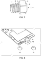
- FIG. 7 illustrates an outer body 1, a cylindrical stage 2, a recess 3 between the outer body 1, a cylindrical stage 5, a bore hole 6 which may include inner thread (or threads) (not shown), distal outer thread (or threads) 7 and proximal outer thread (or threads) 8.
- the distal outer thread 7 and the proximal outer thread 8, which together may make up an outer thread may extend on an outer surface of the cylindrical stage an entire length of the cylindrical stage 5 or less than the entire length of the cylindrical stage 5.
- the double-threaded connector or spacer in accordance with principles of the present disclosure facilitates exchange of the daughter card on a PCB. That is, the double-threaded connector or spacer can be removed from the PCB from the "top" side of the carrier without having to remove solder or to access the "under” side of the carrier simply be unscrewing or otherwise detaching the double-threaded connector or spacer from the top side. Thus a different size / length daughter card can be reinstalled at the new position using the double-threaded connector or spacer. The exchange can be done from one side. It is not necessary to disassemble the carrier in order to get access from the bottom.
- FIG. 8 illustrates the installation of a daughter card to a carrier using a double-threaded connector or spacer according to principles of the present disclosure.
- a double-threaded connector or spacer 12 is installed in a mounting hole 14 of a carrier 11.
- a "half circle" portion 15 of daughter card 9 is held in place between the double-threaded connector or spacer 12 and screw 13.
- the half circle portion 15 of the daughter card is plated to make electrical contact with the double-threaded connector or spacer 12, for example, to allow for grounding of the daughter card 9 via the carrier 11, e.g., PCB.
- an outer surface of the cylindrical stage may include an outer surface electrically conductive layer and the daughter board may include a daughter board electrically conductive region 15 so that the daughter board 9 is electrically connected to the mother board 11 via the daughter board electrically conductive region 15, the outer surface electrically conductive layer of the double-threaded connector 12 and the cylindrical plate 16.
Landscapes
- Engineering & Computer Science (AREA)
- Microelectronics & Electronic Packaging (AREA)
- General Engineering & Computer Science (AREA)
- Theoretical Computer Science (AREA)
- Manufacturing & Machinery (AREA)
- Mechanical Engineering (AREA)
- Computer Hardware Design (AREA)
- Power Engineering (AREA)
- Human Computer Interaction (AREA)
- Physics & Mathematics (AREA)
- General Physics & Mathematics (AREA)
- Coupling Device And Connection With Printed Circuit (AREA)
Abstract
Description
- The present disclosure relates to a connector or spacer for use within an electronic assembly to provide mounting and fixation capability in general for any kind of daughter cards, specifically a double-threaded connector or spacer.
- Electronic devices and electronic assemblies often have a modular concept. The benefit of a modular concept is flexibility and specialization. For example, an Industrial Personal Computer (IPC), may be constructed and designed either with a monolithic PCBA (Printed Circuit Board Assembly) or may have modularity. One example of a modular design may have a (Computer-on-Module) COM Express ® Module, a carrier (e.g., a PCBA), which may provide Input/Output (IO) connectivity, and various daughter cards.
-
FIG. 1 illustrates examples of a standard daughter M.2 modules, which are merely provided herein for reference, but the disclosure is not limited to use only with M.2 modules. That is, the principles described herein may applicable to any daughter module installation on a carrier. M.2 modules are available in different sizes, such as 42mm, 60m and 80mm. The modularity and the exchangeability are great advantages of those modules. -
FIG. 2 illustrates the installation of a module to a carrier. The fixation of the exemplary module is realized with a solder in nut and a screw, which clamps the module. That is, as illustrated in the example ofFIG. 2 , a carrier, e.g., a printed circuit board (PCB) 210 includes plurality of components, including plurality ofmounting holes 214. Themounting holes 214 have different locations on thePCB 210 to accommodate different sized modules. To mount anexemplary module 212 on the PCB, an "off the shelf' solder in nut is installed using a surface-mount technology (SMT) soldering process. In such process, solder innut 216 is provided in thePCB 210 for the mounting of the module. Themodule 212, which may include a half-circle cut out at one end for mounting, is placed to abut the nut, pressed into place, and ascrew 218 is inserted into the nut to secure the module. - This is approach works well as long the size of module required is known in advance of the SMT soldering process. For example, it is difficult to exchange a module once it is installed to replace it with a module of a different size, e.g., for a larger or smaller module. The difficulty arises because the solder in nut would need to be moved in order to the position the new module of different size. Such solder removal is nearly impossible to do in the field and could result in damage to the module, the board or the nut. Therefore, such "in-the-field" module change is impractical. Moreover, it is difficult to provide in advance all the solder in nuts in the board to accommodate later module change because the provided solder in nuts would interfere with the location and positioning of the modules. Other solutions on the market with spacers and nuts are not user-friendly because they require access from both sides of the carrier.
- In accordance with the purpose(s) of this disclosure, as embodied and broadly described herein, this disclosure, in one aspect, relates to a component for installation on a carrier that includes an outer body; a cylindrical cap on the outer body and having a width less than a width of the outer body; a cylindrical stage extending from the outer body in a direction opposite the cylindrical cap; a threaded bore extending through the cylindrical cap and outer body and into the cylindrical stage; and an outer thread extending on an external surface of the cylindrical stage.
- In an aspect, the disclosure relates to a printed circuit board, comprising a carrier having at least one mounting hole there through; a daughter board having a mounting recess along a side thereof; a component extending through one of the at least one mounting holes; the component comprising: an outer body; a cylindrical cap on the outer body and having a diameter less than a width of the outer body; a cylindrical stage extending from the outer body in a direction opposite the cylindrical cap and having a diameter less than a width of the outer body; a threaded bore extending through the cylindrical cap and outer body and into the cylindrical stage; an outer thread extending on an external surface of the cylindrical stage; and a screw extending through the threaded bore; wherein a portion of the daughter board contacts the component.
- In an aspect, the disclosure relates to a method of installing a daughter board on a mother board, comprising threading a component into a mounting hole on the mother board, the component comprising: an outer body; a cylindrical cap on the outer body and having a diameter less than a width of the outer body; a cylindrical stage extending from the outer body in a direction opposite the cylindrical cap and having a diameter less than a width the outer body ; a threaded bore extending through the cylindrical cap and outer body and terminating within the cylindrical stage; an outer thread extending on an external surface of the cylindrical stage; providing a daughter card adjacent the component; and applying a screw in the threaded bore causing the component to removably clamp the daughter board to the component.
- Additional advantages of the disclosure will be set forth in part in the description which follows, and in part will be obvious from the description, or may be learned by practice of the disclosure. The advantages of the disclosure will be realized and attained by means of the elements and combinations particularly pointed out in the appended claims. It is to be understood that both the foregoing general description and the following detailed description are exemplary and explanatory only and are not restrictive of the disclosure, as claimed.
- An advantage of the present disclosure is to provide an adaptable, multiple application system for attaching a daughter module to a carrier. Advantages of the present disclosure include post-factory ("in the field") removal and installation of modules without having to remove soldered-in pieces or causing damage to the modules or boards or other components.
- Further examples, features, and advantages of the double-threaded spacer, as well as the structure and operation of the various examples of the double-threaded spacer, are described in detail below with reference to the accompanying drawings.
- It is to be understood that both the foregoing general description and the following detailed description are exemplary and explanatory only, and are not restrictive of the claims.
- The accompanying figures, which are incorporated herein and form part of the specification, illustrate the double-threaded connector. Together with the description, the figures further serve to explain the principles of the double-threaded connector described herein and thereby enable a person skilled in the pertinent art to make and use the double-threaded connector.
-
FIG. 1 is illustrates non-limiting examples of daughter card modules that can be mounted through use of an example of the present. -
FIG. 2 illustrates the installation of a short daughter cared on a carrier. -
FIG. 3 illustrates a double-threaded connector according to principles of the present disclosure. -
FIG. 4A illustrates a cross-sectional view of an example of the double-threaded connector according to principles of the present disclosure. -
FIG. 4B illustrates a side view of an example of the double-threaded connector according to principles of the present disclosure. -
FIG. 4C illustrates a side view of an example of the double-threaded connector without threads according to principles of the present disclosure. -
FIG. 4D illustrates a top view of an example of the double-threaded connector according to principles of the present disclosure. -
FIG. 4E illustrates an alternative example of the present disclosure in which some threads are replaced by a smooth cylinder. -
FIG. 5 illustrates the usage of the double-threaded spacer according to principles of the present disclosure. -
FIGs. 6A and B illustrate aspects of the electrically conductive cylinder on the carrier. -
FIG. 7 illustrates an example of the present disclosure; -
FIG. 8 illustrates the installation of a daughter card to a carrier using a double-threaded connector according to principles of the present disclosure. - Reference will now be made in detail to examples of the double-threaded connector or spacer with reference to the accompanying figures, in which like reference numerals indicate like elements.
- It will be apparent to those skilled in the art that various modifications and variations can be made in the present disclosure without departing from the spirit or scope of the disclosure. Thus, it is intended that the present disclosure cover the modifications and variations of this disclosure provided they come within the scope of the appended claims and their equivalents.
-
FIG. 3 illustrates a double-threaded connector or spacer according to principles of the present disclosure that allow for installation and replacement of modules of various sizes on a carrier. While the term "spacer" is used herein to refer to the component detailed herein, the component is not limited to performing a spacer function and is not required to perform a spacing function. As illustrated in theFIG. 3 , an exemplary double-threaded connector, spacer or component according to principles of the present disclosure includes at least the following geometrical features: anouter body 1, acylindrical stage 2, arecess 3 between theouter body 1 and anouter thread 4, acylindrical stage 5, and abore hole 6 may include inner threads (not shown). The inner thread may be of pitch to receive an "off the shelf' screw of predetermined diameter and thread, but is not so limited. Theouter body 1 may be hexagonal to accommodate a hexagon spanner. - The
cylindrical stage 2 is sized to align with a half-circle cut out at one end of a module for mounting (seeFIG. 5 ). Thecylindrical stage 5 is sized in relation to a mounting hole diameter in the PCB. Thecylindrical stage 5 enables the right angled / upright installation of the double-threaded connector or spacer into the PCB. Thecylindrical stage 2 may provide for adjustment of the daughter card relative to the connector and the double-threaded connector or spacer. - The double-threaded connector or spacer according to principles of the present disclosure may be self-threading such that insertion into a mounting hole in a PCB will cause the interior of the mounting hole to become threaded to match the double-threaded connector or spacer, for example, by deforming the material of the PCB. As illustrated in
FIG. 4 , the self-threading feature of the double-threaded connector or spacer according to principles of the present disclosure may include a plurality of distal thread (or threads) 7 at a distal end of the double-threaded connector or spacer, where the plurality of distal thread (or threads) 7 may be compatible with regularly (e.g., "off-the-shelf') machined threads. Such regularly machined threads may be for use with a solder in nut on the underside of the carrier, such as a PCB. In place of thedistal threads 7 may be a smooth cylinder adjacent a plurality of proximalouter threads 8. The self-threading feature of the double-threaded connector or spacer may be facilitated by hills of the distal thread (or threads) 7 having a circular or arcuate topology at a distal end ofcylindrical stage 5 of the double-threaded connector or spacer such that the thread (or threads) assists in first movement of thecylindrical stage 5 into a PCB mounting hole (not shown inFIG. 3 ). The proximal outer thread (or threads) 8 in the proximal portion of thecylindrical stage 5 may have the same profile as or a different profile than the distal thread (or threads) 7 in the distal portion of the double-threaded connector or spacer. In other examples, all of the threads of the may be "circular" or "arcuate" or "off-the-shelf or angular. That is, theouter thread 4 may have a thread so that the double-threaded connector or spacer can be screwed into a solder in nut, for example, mounted on the underside of the carrier or PCB. In an example for mounting an M4 board, the diameter of the proximal outer thread (or threads) 8 would be 3.75mm, but this disclosure is not so limited and the thread diameter may range, for example, from 3.5mm to 3.8mm. - The double-threaded connector or spacer according to principles of the present disclosure is further illustrated in
FIGs. 4A-D. FIG. 4A illustrates a cross-sectional view of an example of the double-threaded connector or spacer according to principles of the present disclosure.FIG. 4B illustrates a side view of an example of the double-threaded connector or spacer according to principles of the present disclosure.FIG. 4C illustrates a side view of an example of the double-threaded connector or spacer without threads according to principles of the present disclosure.FIG. 4D illustrates a top view of an example of the double-threaded connector or spacer according to principles of the present disclosure.FIG. 4E illustrates an alternative example of the present disclosure in which some threads are replaced by a substantially smooth cylinder. As illustrated inFIGS. 4A-D , an exemplary double-threaded connector or spacer or component according to principles of the present disclosure includes at least the following geometrical features: anouter body 1, acylindrical stage 2, arecess 3 between theouter body 1, acylindrical stage 5, abore hole 6 which may include inner thread (or threads) (not shown), distal outer thread (or threads) 7 and proximal outer thread (or threads) 8. -
FIG. 5 illustrates the usage of the double-threaded connector or spacer according to principles of the present disclosure. As illustrated in cross-section, a daughter card/module 9, aconnector 10, acarrier 11, a double-threaded connector orspacer 12, and ascrew 18 is shown. The double-threaded connector orspacer 12 can be installed to the required position depending on the size of the daughter card (e.g., M.2 Module). According to principles of the present disclosure, the double-threaded connector orspacer 12 is screwed directly into the carrier orPCB 11, for example, into a mountinghole 14. As illustrated inFIG. 4 , the mounting holes may be located in the carrier to accommodate various daughter card sizes, which may be commercial or standard, such as 42mm, 60mm and 80mm. The mounting hole diameter in the PCB is in relation to theouter thread 4. That is, the outer thread (or threads) 4 of the double-threaded connector or spacer are sized to be accommodated appropriately in the mounting holes 14. A screw 13 is used to clamp thedaughter card 9 to the double-threaded connector orspacer 12. - The mounting holes in the carrier or
PCB 11 may be plated with conductive metal, such as copper or other known conductive metal, or may be unplated, to facilitate reliable electrical contact for grounding of the daughter card to the mother card or other purpose. The mounting hole may be electrically connected pad at the top side if the daughter card needs grounding. The diameter of the mounting hole will depend on the interior mounting hole finish (e.g., plated or not). In addition, the diameter of the mounting hole is a function of the torque force to be applied during installation and the tightness of the installed double-threaded connector or spacer. Also, the acceptable deformation in the PCB and the mounting hole also is considered in determining the diameter of the mounting hole. -
FIGs. 6A and 6B illustrate a cut-away section of thePCB 11 at a mountinghole 14. As illustrated inFIGs. 6A and 6B , the mountinghole 14 of thecarrier 11, for example, a PCB, may include a metalizedcylinder 16 or cylindrical plate that makes contact with the underside of the double-threaded connector or spacer (not shown) when the double-threaded connector or spacer (not shown) is mounted on the carrier/PCB. The diameter of the board hole may range from about 3.5mm to about 3.8mm, but need not be so limited and may be as appropriate for the carrier used and the daughter card or board chosen for mounting. Thecylinder 16 includes a center hole or central opening17. As illustrated inFIG. 6A , the size (diameter) of thecenter hole 17 may be substantially matched to the size (diameter) of the mountinghole 14 in thecarrier 11. In an aspect, thecenter hole 17 size (diameter) may be larger than the size (diameter) of the mountinghole 14 such that a "gap ring" 18 of carrier may exist around the mounting hole. Thecylinder 16 may be made of metal or metal alloy or other electrically conductive material or may be made of any suitable material that is coated with metal to create an electrically conductive contact. If the material making up the cylinder is not electrically conductive, or is not sufficiently electrically conductive, the cylinder may be fully or partially plated with an electrically conductive material to form an electrically conductive layer on an outer surface of the cylinder or cylindrical stage, as determined by the application of the device. In some aspects, torque force is applied to the double-threaded connector or spacer for insertion into a mountinghole 14 having acylinder 16 such that the bottom surface of theouter body 1 of the double-threaded connector or spacer makes contact with an upper surface of thecylinder 16 to create an electrical contact between the cylinder and the double-threaded connector or spacer, which itself is in electrical contact with daughter card/module 9. - The double-threaded connector or spacer may be made of metal, as illustrated in
FIG. 7 , or may be made of any other suitable material, electrically conductive or not. If the material making up the double-threaded connector or spacer is not electrically conductive, or is not sufficiently electrically conductive, the surface of the double-threaded connector or spacer may be fully or partially electrically conductive, as determined by the application of the device. The surface may be made electrically conductive, by, for example, coating or plating on the surface of the double-threaded connector or spacer.FIG. 7 illustrates anouter body 1, acylindrical stage 2, arecess 3 between theouter body 1, acylindrical stage 5, abore hole 6 which may include inner thread (or threads) (not shown), distal outer thread (or threads) 7 and proximal outer thread (or threads) 8. As illustrated, the distalouter thread 7 and the proximalouter thread 8, which together may make up an outer thread, may extend on an outer surface of the cylindrical stage an entire length of thecylindrical stage 5 or less than the entire length of thecylindrical stage 5. - In use, the double-threaded connector or spacer in accordance with principles of the present disclosure facilitates exchange of the daughter card on a PCB. That is, the double-threaded connector or spacer can be removed from the PCB from the "top" side of the carrier without having to remove solder or to access the "under" side of the carrier simply be unscrewing or otherwise detaching the double-threaded connector or spacer from the top side. Thus a different size / length daughter card can be reinstalled at the new position using the double-threaded connector or spacer. The exchange can be done from one side. It is not necessary to disassemble the carrier in order to get access from the bottom.
-
FIG. 8 illustrates the installation of a daughter card to a carrier using a double-threaded connector or spacer according to principles of the present disclosure. As shown, a double-threaded connector orspacer 12 is installed in a mountinghole 14 of acarrier 11. A "half circle" portion 15 ofdaughter card 9 is held in place between the double-threaded connector orspacer 12 and screw 13. As can be seen, the half circle portion 15 of the daughter card is plated to make electrical contact with the double-threaded connector orspacer 12, for example, to allow for grounding of thedaughter card 9 via thecarrier 11, e.g., PCB. For example, an outer surface of the cylindrical stage may include an outer surface electrically conductive layer and the daughter board may include a daughter board electrically conductive region 15 so that thedaughter board 9 is electrically connected to themother board 11 via the daughter board electrically conductive region 15, the outer surface electrically conductive layer of the double-threadedconnector 12 and thecylindrical plate 16. - While various examples of the present disclosure have been described above, it should be understood that they have been presented by way of example only, and not limitation. Thus, the breadth and scope of the present disclosure should not be limited by any of the above-described exemplary examples, but should be defined in accordance with the following claims and their equivalents.
Claims (15)
- A component for installation on a carrier, comprising:an outer body;a cylindrical cap on the outer body and having a width less than a width of the outer body;a cylindrical stage extending from the outer body in a direction opposite the cylindrical cap;a threaded bore extending through the cylindrical cap and outer body and into the cylindrical stage; andan outer thread extending on an external surface of the cylindrical stage.
- The component of claim 1, wherein the threaded bore terminates within the cylindrical stage.
- The component of claim 1, further comprising an electrically conductive layer on at least a portion of an outer surface of the cylindrical stage.
- The component of claim 1, further comprising:
a recess between the outer body and the outer thread. - The component of claim 1, wherein the outer thread extends on a portion of an outer surface of the cylindrical stage less than an entire length of the cylindrical stage, wherein a distal portion of the external surface of the cylindrical stage does not include the outer thread.
- A printed circuit board, comprising:a carrier having at least one mounting hole there through;a daughter board having a mounting recess along a side thereof;a component extending through one of the at least one mounting holes; the component comprising:an outer body;a cylindrical cap on the outer body and having a diameter less than a width of the outer body;a cylindrical stage extending from the outer body in a direction opposite the cylindrical cap and having a diameter less than a width of the outer body;a threaded bore extending through the cylindrical cap and outer body and into the cylindrical stage; andan outer thread extending on an external surface of the cylindrical stage; anda screw extending through the threaded bore;wherein a portion of the daughter board contacts the component.
- The printed circuit board of claim 6, wherein the portion of the daughter board that contacts the component is the mounting recess.
- The printed circuit board of claim 6, wherein the cylindrical cap of the component contacts the daughter board and/or the outer body of the component contacts the daughter board.
- The printed circuit board of claim 6, further comprising a cylindrical plate having a central opening on an upper surface of the carrier.
- The printed circuit board of claim 9, wherein a diameter of the at least one mounting hole corresponds to a diameter of the central opening of the cylindrical plate or the diameter of the at least one mounting hole is less than a diameter of the central opening of the cylindrical plate.
- A method of installing a daughter board on a mother board, comprising:threading a component into a mounting hole on the mother board, the component comprising:an outer body; a cylindrical cap on the outer body and having a diameter less than a width of the outer body;a cylindrical stage extending from the outer body in a direction opposite the cylindrical cap and having a diameter less than a width the outer body;a threaded bore extending through the cylindrical cap and outer body and into the cylindrical stage;an outer thread extending on an external surface of the cylindrical stage;providing a daughter board adjacent the component; andapplying a screw in the threaded bore causing the component to removably clamp the daughter board to the component.
- The method of claim 11, further comprising an electrically conductive layer on at least a portion of an outer surface of the cylindrical stage.
- The method of claim 11, wherein the mother board includes a cylindrical plate having a central opening on an upper surface of the mother board.
- The method of claim 13, wherein a diameter of the mounting hole corresponds to a diameter of the central opening of the cylindrical plate or is less than a diameter of the central opening of the cylindrical plate.
- The method of claim 13, wherein an outer surface of the cylindrical stage includes an outer surface electrically conductive layer and the daughter board includes a daughter board electrically conductive region, the method further comprising electrically connecting the daughter board to the mother board via the daughter board electrically conductive region, the outer surface electrically conductive layer and the cylindrical plate.
Applications Claiming Priority (1)
| Application Number | Priority Date | Filing Date | Title |
|---|---|---|---|
| US15/597,957 US10103466B1 (en) | 2017-05-17 | 2017-05-17 | Double-threaded connector |
Publications (2)
| Publication Number | Publication Date |
|---|---|
| EP3404507A1 true EP3404507A1 (en) | 2018-11-21 |
| EP3404507B1 EP3404507B1 (en) | 2024-12-25 |
Family
ID=62222403
Family Applications (1)
| Application Number | Title | Priority Date | Filing Date |
|---|---|---|---|
| EP18172980.7A Active EP3404507B1 (en) | 2017-05-17 | 2018-05-17 | Double-threaded connector and spacer |
Country Status (2)
| Country | Link |
|---|---|
| US (1) | US10103466B1 (en) |
| EP (1) | EP3404507B1 (en) |
Cited By (1)
| Publication number | Priority date | Publication date | Assignee | Title |
|---|---|---|---|---|
| EP4621251A1 (en) * | 2024-03-18 | 2025-09-24 | TE Connectivity Solutions GmbH | Threaded insert and contact assembly with threaded insert |
Families Citing this family (8)
| Publication number | Priority date | Publication date | Assignee | Title |
|---|---|---|---|---|
| US10488893B1 (en) * | 2018-05-23 | 2019-11-26 | Dell Products L.P. | Expansion module system |
| CN112533369B (en) * | 2019-09-18 | 2022-08-09 | 华为技术有限公司 | Circuit assembly and electronic device |
| JP7315500B2 (en) * | 2020-03-03 | 2023-07-26 | Necパーソナルコンピュータ株式会社 | Portable information equipment and substrates |
| US11262813B2 (en) * | 2020-05-05 | 2022-03-01 | Quanta Computer Inc. | Double-sided and tool-less M.2 module design |
| CN111867246A (en) * | 2020-08-11 | 2020-10-30 | 东莞市卓品电子科技有限公司 | A PCB module structure and circuit board assembly |
| FR3126068B1 (en) * | 2021-08-04 | 2023-06-30 | Safran Electronics & Defense | DEVICE FOR STIFFENING AN M.2 TYPE CONNECTOR |
| DE102021127209A1 (en) | 2021-10-20 | 2023-04-20 | Fujitsu Client Computing Limited | Circuit board, computer assembly and connector |
| US20240021333A1 (en) * | 2022-07-18 | 2024-01-18 | Westinghouse Electric Company Llc | Devices, systems, and methods for enhancing the implementation of control circuits for nuclear instrumentation and control systems |
Citations (6)
| Publication number | Priority date | Publication date | Assignee | Title |
|---|---|---|---|---|
| EP2354826A1 (en) * | 2010-02-04 | 2011-08-10 | Corning Cable Systems LLC | Communications equipment housings, assemblies, and related alignment features and methods |
| US20120168584A1 (en) * | 2010-12-29 | 2012-07-05 | Hon Hai Precision Industry Co., Ltd. | Fixing device for circuit board |
| US20130259601A1 (en) * | 2012-03-30 | 2013-10-03 | Alcatel-Lucent Canada, Inc. | Low Profile Standoff With Tool Stop |
| US20140211432A1 (en) * | 2013-01-30 | 2014-07-31 | Apple Inc. | Multipurpose fastener for electronic devices |
| US20150144376A1 (en) * | 2013-11-28 | 2015-05-28 | Fujitsu Limited | Electronic device and spacing tube |
| US20170131748A1 (en) * | 2015-11-06 | 2017-05-11 | Kabushiki Kaisha Toshiba | Length-adjustable storage device |
Family Cites Families (11)
| Publication number | Priority date | Publication date | Assignee | Title |
|---|---|---|---|---|
| US5173842A (en) | 1991-09-27 | 1992-12-22 | International Business Machines Corporation | Electrical assembly with deformable bridge printed circuit board |
| EP0608221B1 (en) | 1991-10-17 | 1996-12-11 | Itt Industries, Inc. | Interconnector |
| US6280202B1 (en) * | 1999-09-01 | 2001-08-28 | Thomas & Betts International, Inc. | Board-to-board alignment and securement device |
| US6493233B1 (en) * | 2001-08-21 | 2002-12-10 | Intel Corporation | PCB-to-chassis mounting schemes |
| US6875940B2 (en) | 2003-07-25 | 2005-04-05 | Leviton Manufacturing Co., Inc. | Robust rocker switch mechanism |
| US8366745B2 (en) | 2007-05-01 | 2013-02-05 | Jackson Roger P | Dynamic stabilization assembly having pre-compressed spacers with differential displacements |
| JP2012104600A (en) | 2010-11-09 | 2012-05-31 | Nifco Inc | Spacer device |
| DE112014005338T5 (en) * | 2013-11-22 | 2016-09-29 | Samtec, Inc. | Two-piece solution-supporting spacer |
| TWM475794U (en) * | 2013-12-02 | 2014-04-01 | Giga Byte Tech Co Ltd | Stud |
| DE102013114213B4 (en) | 2013-12-17 | 2022-10-13 | Infineon Technologies Ag | Probe card and method of manufacturing a probe card |
| CN105305309B (en) | 2015-09-01 | 2017-09-15 | 孝感先源电力有限责任公司 | Circuit obstacle crossing type driving |
-
2017
- 2017-05-17 US US15/597,957 patent/US10103466B1/en active Active
-
2018
- 2018-05-17 EP EP18172980.7A patent/EP3404507B1/en active Active
Patent Citations (6)
| Publication number | Priority date | Publication date | Assignee | Title |
|---|---|---|---|---|
| EP2354826A1 (en) * | 2010-02-04 | 2011-08-10 | Corning Cable Systems LLC | Communications equipment housings, assemblies, and related alignment features and methods |
| US20120168584A1 (en) * | 2010-12-29 | 2012-07-05 | Hon Hai Precision Industry Co., Ltd. | Fixing device for circuit board |
| US20130259601A1 (en) * | 2012-03-30 | 2013-10-03 | Alcatel-Lucent Canada, Inc. | Low Profile Standoff With Tool Stop |
| US20140211432A1 (en) * | 2013-01-30 | 2014-07-31 | Apple Inc. | Multipurpose fastener for electronic devices |
| US20150144376A1 (en) * | 2013-11-28 | 2015-05-28 | Fujitsu Limited | Electronic device and spacing tube |
| US20170131748A1 (en) * | 2015-11-06 | 2017-05-11 | Kabushiki Kaisha Toshiba | Length-adjustable storage device |
Cited By (2)
| Publication number | Priority date | Publication date | Assignee | Title |
|---|---|---|---|---|
| EP4621251A1 (en) * | 2024-03-18 | 2025-09-24 | TE Connectivity Solutions GmbH | Threaded insert and contact assembly with threaded insert |
| JP2025143229A (en) * | 2024-03-18 | 2025-10-01 | ティーイー コネクティビティ ソリューソンズ ゲーエムベーハー | Threaded insert and contact assembly having threaded insert - Patent application |
Also Published As
| Publication number | Publication date |
|---|---|
| US10103466B1 (en) | 2018-10-16 |
| EP3404507B1 (en) | 2024-12-25 |
Similar Documents
| Publication | Publication Date | Title |
|---|---|---|
| EP3404507B1 (en) | Double-threaded connector and spacer | |
| US7575443B2 (en) | Combined fastening and contacting system for electrical components on superimposed circuit boards | |
| DE102007001407B4 (en) | Mounting arrangement for fixing superposed printed circuit boards in a housing | |
| US9520658B1 (en) | Fastener assembly | |
| US6416330B1 (en) | Canted coil spring conductor electrical circuit connector | |
| US8929077B2 (en) | Thermal connector | |
| EP2083489A1 (en) | Connection element to electrically connect an LED | |
| US20150211718A1 (en) | Flexible printed circuit board for electrically contacting and mechanically fixing a lamp in a luminaire | |
| US20130265731A1 (en) | Circuit board system | |
| EP2347639A1 (en) | Illumination device comprising two printed circuit boards | |
| WO2006056512A1 (en) | Electronic device | |
| US20060037776A1 (en) | Securable electronic module | |
| US9590329B2 (en) | Pin attach converter | |
| CN202468638U (en) | PCB (Printed Circuit Board) welding nut and circuit board | |
| DE102016000762A1 (en) | electrical appliance | |
| US20170164491A1 (en) | Surface Mounted Fastener | |
| CN115732950B (en) | Connector and method for connecting a circuit board to at least one conductor | |
| US6404650B1 (en) | System for connecting a module comprising a plurality of electronic cards to a backplane | |
| EP2911487A1 (en) | Circuit board mounting arrangement | |
| JP3072629U (en) | Electrical equipment using flat flexible substrates | |
| US9402320B2 (en) | Electronic component assembly | |
| US7364441B2 (en) | Low-profile PCI adapter cards with high port counts | |
| JP2013179011A (en) | Circuit board | |
| EP1589618A1 (en) | Electronic device with a contact pin and method for producing such a device | |
| US8939791B2 (en) | Primary circuit board non-conductive void having different planar dimensions through board thickness to secure non-conducting locking member of holder |
Legal Events
| Date | Code | Title | Description |
|---|---|---|---|
| PUAI | Public reference made under article 153(3) epc to a published international application that has entered the european phase |
Free format text: ORIGINAL CODE: 0009012 |
|
| STAA | Information on the status of an ep patent application or granted ep patent |
Free format text: STATUS: THE APPLICATION HAS BEEN PUBLISHED |
|
| AK | Designated contracting states |
Kind code of ref document: A1 Designated state(s): AL AT BE BG CH CY CZ DE DK EE ES FI FR GB GR HR HU IE IS IT LI LT LU LV MC MK MT NL NO PL PT RO RS SE SI SK SM TR |
|
| AX | Request for extension of the european patent |
Extension state: BA ME |
|
| STAA | Information on the status of an ep patent application or granted ep patent |
Free format text: STATUS: REQUEST FOR EXAMINATION WAS MADE |
|
| 17P | Request for examination filed |
Effective date: 20190520 |
|
| RBV | Designated contracting states (corrected) |
Designated state(s): AL AT BE BG CH CY CZ DE DK EE ES FI FR GB GR HR HU IE IS IT LI LT LU LV MC MK MT NL NO PL PT RO RS SE SI SK SM TR |
|
| RAP1 | Party data changed (applicant data changed or rights of an application transferred) |
Owner name: INTELLIGENT PLATFORMS, LLC |
|
| STAA | Information on the status of an ep patent application or granted ep patent |
Free format text: STATUS: EXAMINATION IS IN PROGRESS |
|
| 17Q | First examination report despatched |
Effective date: 20220421 |
|
| GRAP | Despatch of communication of intention to grant a patent |
Free format text: ORIGINAL CODE: EPIDOSNIGR1 |
|
| STAA | Information on the status of an ep patent application or granted ep patent |
Free format text: STATUS: GRANT OF PATENT IS INTENDED |
|
| INTG | Intention to grant announced |
Effective date: 20240718 |
|
| GRAS | Grant fee paid |
Free format text: ORIGINAL CODE: EPIDOSNIGR3 |
|
| GRAA | (expected) grant |
Free format text: ORIGINAL CODE: 0009210 |
|
| STAA | Information on the status of an ep patent application or granted ep patent |
Free format text: STATUS: THE PATENT HAS BEEN GRANTED |
|
| AK | Designated contracting states |
Kind code of ref document: B1 Designated state(s): AL AT BE BG CH CY CZ DE DK EE ES FI FR GB GR HR HU IE IS IT LI LT LU LV MC MK MT NL NO PL PT RO RS SE SI SK SM TR |
|
| REG | Reference to a national code |
Ref country code: GB Ref legal event code: FG4D |
|
| REG | Reference to a national code |
Ref country code: CH Ref legal event code: EP |
|
| REG | Reference to a national code |
Ref country code: DE Ref legal event code: R096 Ref document number: 602018077879 Country of ref document: DE |
|
| REG | Reference to a national code |
Ref country code: IE Ref legal event code: FG4D |
|
| REG | Reference to a national code |
Ref country code: LT Ref legal event code: MG9D |
|
| PG25 | Lapsed in a contracting state [announced via postgrant information from national office to epo] |
Ref country code: HR Free format text: LAPSE BECAUSE OF FAILURE TO SUBMIT A TRANSLATION OF THE DESCRIPTION OR TO PAY THE FEE WITHIN THE PRESCRIBED TIME-LIMIT Effective date: 20241225 |
|
| PG25 | Lapsed in a contracting state [announced via postgrant information from national office to epo] |
Ref country code: FI Free format text: LAPSE BECAUSE OF FAILURE TO SUBMIT A TRANSLATION OF THE DESCRIPTION OR TO PAY THE FEE WITHIN THE PRESCRIBED TIME-LIMIT Effective date: 20241225 |
|
| PG25 | Lapsed in a contracting state [announced via postgrant information from national office to epo] |
Ref country code: BG Free format text: LAPSE BECAUSE OF FAILURE TO SUBMIT A TRANSLATION OF THE DESCRIPTION OR TO PAY THE FEE WITHIN THE PRESCRIBED TIME-LIMIT Effective date: 20241225 |
|
| PG25 | Lapsed in a contracting state [announced via postgrant information from national office to epo] |
Ref country code: NO Free format text: LAPSE BECAUSE OF FAILURE TO SUBMIT A TRANSLATION OF THE DESCRIPTION OR TO PAY THE FEE WITHIN THE PRESCRIBED TIME-LIMIT Effective date: 20250325 |
|
| PG25 | Lapsed in a contracting state [announced via postgrant information from national office to epo] |
Ref country code: GR Free format text: LAPSE BECAUSE OF FAILURE TO SUBMIT A TRANSLATION OF THE DESCRIPTION OR TO PAY THE FEE WITHIN THE PRESCRIBED TIME-LIMIT Effective date: 20250326 Ref country code: LV Free format text: LAPSE BECAUSE OF FAILURE TO SUBMIT A TRANSLATION OF THE DESCRIPTION OR TO PAY THE FEE WITHIN THE PRESCRIBED TIME-LIMIT Effective date: 20241225 |
|
| PG25 | Lapsed in a contracting state [announced via postgrant information from national office to epo] |
Ref country code: RS Free format text: LAPSE BECAUSE OF FAILURE TO SUBMIT A TRANSLATION OF THE DESCRIPTION OR TO PAY THE FEE WITHIN THE PRESCRIBED TIME-LIMIT Effective date: 20250325 |
|
| REG | Reference to a national code |
Ref country code: NL Ref legal event code: MP Effective date: 20241225 |
|
| PG25 | Lapsed in a contracting state [announced via postgrant information from national office to epo] |
Ref country code: NL Free format text: LAPSE BECAUSE OF FAILURE TO SUBMIT A TRANSLATION OF THE DESCRIPTION OR TO PAY THE FEE WITHIN THE PRESCRIBED TIME-LIMIT Effective date: 20241225 |
|
| REG | Reference to a national code |
Ref country code: AT Ref legal event code: MK05 Ref document number: 1754728 Country of ref document: AT Kind code of ref document: T Effective date: 20241225 |
|
| PG25 | Lapsed in a contracting state [announced via postgrant information from national office to epo] |
Ref country code: SM Free format text: LAPSE BECAUSE OF FAILURE TO SUBMIT A TRANSLATION OF THE DESCRIPTION OR TO PAY THE FEE WITHIN THE PRESCRIBED TIME-LIMIT Effective date: 20241225 |
|
| PG25 | Lapsed in a contracting state [announced via postgrant information from national office to epo] |
Ref country code: PL Free format text: LAPSE BECAUSE OF FAILURE TO SUBMIT A TRANSLATION OF THE DESCRIPTION OR TO PAY THE FEE WITHIN THE PRESCRIBED TIME-LIMIT Effective date: 20241225 |
|
| PG25 | Lapsed in a contracting state [announced via postgrant information from national office to epo] |
Ref country code: ES Free format text: LAPSE BECAUSE OF FAILURE TO SUBMIT A TRANSLATION OF THE DESCRIPTION OR TO PAY THE FEE WITHIN THE PRESCRIBED TIME-LIMIT Effective date: 20241225 |
|
| PG25 | Lapsed in a contracting state [announced via postgrant information from national office to epo] |
Ref country code: IS Free format text: LAPSE BECAUSE OF FAILURE TO SUBMIT A TRANSLATION OF THE DESCRIPTION OR TO PAY THE FEE WITHIN THE PRESCRIBED TIME-LIMIT Effective date: 20250425 |
|
| PG25 | Lapsed in a contracting state [announced via postgrant information from national office to epo] |
Ref country code: PT Free format text: LAPSE BECAUSE OF FAILURE TO SUBMIT A TRANSLATION OF THE DESCRIPTION OR TO PAY THE FEE WITHIN THE PRESCRIBED TIME-LIMIT Effective date: 20250428 |
|
| PG25 | Lapsed in a contracting state [announced via postgrant information from national office to epo] |
Ref country code: EE Free format text: LAPSE BECAUSE OF FAILURE TO SUBMIT A TRANSLATION OF THE DESCRIPTION OR TO PAY THE FEE WITHIN THE PRESCRIBED TIME-LIMIT Effective date: 20241225 |
|
| PG25 | Lapsed in a contracting state [announced via postgrant information from national office to epo] |
Ref country code: AT Free format text: LAPSE BECAUSE OF FAILURE TO SUBMIT A TRANSLATION OF THE DESCRIPTION OR TO PAY THE FEE WITHIN THE PRESCRIBED TIME-LIMIT Effective date: 20241225 Ref country code: RO Free format text: LAPSE BECAUSE OF FAILURE TO SUBMIT A TRANSLATION OF THE DESCRIPTION OR TO PAY THE FEE WITHIN THE PRESCRIBED TIME-LIMIT Effective date: 20241225 |
|
| PG25 | Lapsed in a contracting state [announced via postgrant information from national office to epo] |
Ref country code: SK Free format text: LAPSE BECAUSE OF FAILURE TO SUBMIT A TRANSLATION OF THE DESCRIPTION OR TO PAY THE FEE WITHIN THE PRESCRIBED TIME-LIMIT Effective date: 20241225 |
|
| PG25 | Lapsed in a contracting state [announced via postgrant information from national office to epo] |
Ref country code: CZ Free format text: LAPSE BECAUSE OF FAILURE TO SUBMIT A TRANSLATION OF THE DESCRIPTION OR TO PAY THE FEE WITHIN THE PRESCRIBED TIME-LIMIT Effective date: 20241225 |
|
| PG25 | Lapsed in a contracting state [announced via postgrant information from national office to epo] |
Ref country code: IT Free format text: LAPSE BECAUSE OF FAILURE TO SUBMIT A TRANSLATION OF THE DESCRIPTION OR TO PAY THE FEE WITHIN THE PRESCRIBED TIME-LIMIT Effective date: 20241225 |
|
| PG25 | Lapsed in a contracting state [announced via postgrant information from national office to epo] |
Ref country code: SE Free format text: LAPSE BECAUSE OF FAILURE TO SUBMIT A TRANSLATION OF THE DESCRIPTION OR TO PAY THE FEE WITHIN THE PRESCRIBED TIME-LIMIT Effective date: 20241225 |
|
| REG | Reference to a national code |
Ref country code: DE Ref legal event code: R097 Ref document number: 602018077879 Country of ref document: DE |
|
| PG25 | Lapsed in a contracting state [announced via postgrant information from national office to epo] |
Ref country code: DK Free format text: LAPSE BECAUSE OF FAILURE TO SUBMIT A TRANSLATION OF THE DESCRIPTION OR TO PAY THE FEE WITHIN THE PRESCRIBED TIME-LIMIT Effective date: 20241225 |
|
| PLBE | No opposition filed within time limit |
Free format text: ORIGINAL CODE: 0009261 |
|
| STAA | Information on the status of an ep patent application or granted ep patent |
Free format text: STATUS: NO OPPOSITION FILED WITHIN TIME LIMIT |
|
| REG | Reference to a national code |
Ref country code: CH Ref legal event code: L10 Free format text: ST27 STATUS EVENT CODE: U-0-0-L10-L00 (AS PROVIDED BY THE NATIONAL OFFICE) Effective date: 20251105 |
|
| REG | Reference to a national code |
Ref country code: DE Ref legal event code: R119 Ref document number: 602018077879 Country of ref document: DE |
|
| 26N | No opposition filed |
Effective date: 20250926 |
|
| REG | Reference to a national code |
Ref country code: CH Ref legal event code: H13 Free format text: ST27 STATUS EVENT CODE: U-0-0-H10-H13 (AS PROVIDED BY THE NATIONAL OFFICE) Effective date: 20251223 |
|
| PG25 | Lapsed in a contracting state [announced via postgrant information from national office to epo] |
Ref country code: LU Free format text: LAPSE BECAUSE OF NON-PAYMENT OF DUE FEES Effective date: 20250517 |
|
| PG25 | Lapsed in a contracting state [announced via postgrant information from national office to epo] |
Ref country code: CH Free format text: LAPSE BECAUSE OF NON-PAYMENT OF DUE FEES Effective date: 20250531 |
|
| GBPC | Gb: european patent ceased through non-payment of renewal fee |
Effective date: 20250517 |
|
| REG | Reference to a national code |
Ref country code: BE Ref legal event code: MM Effective date: 20250531 |
|
| PG25 | Lapsed in a contracting state [announced via postgrant information from national office to epo] |
Ref country code: MC Free format text: LAPSE BECAUSE OF FAILURE TO SUBMIT A TRANSLATION OF THE DESCRIPTION OR TO PAY THE FEE WITHIN THE PRESCRIBED TIME-LIMIT Effective date: 20241225 |
|
| PG25 | Lapsed in a contracting state [announced via postgrant information from national office to epo] |
Ref country code: GB Free format text: LAPSE BECAUSE OF NON-PAYMENT OF DUE FEES Effective date: 20250517 |
|
| PG25 | Lapsed in a contracting state [announced via postgrant information from national office to epo] |
Ref country code: IE Free format text: LAPSE BECAUSE OF NON-PAYMENT OF DUE FEES Effective date: 20250517 Ref country code: DE Free format text: LAPSE BECAUSE OF NON-PAYMENT OF DUE FEES Effective date: 20251202 |
|
| PG25 | Lapsed in a contracting state [announced via postgrant information from national office to epo] |
Ref country code: BE Free format text: LAPSE BECAUSE OF NON-PAYMENT OF DUE FEES Effective date: 20250531 |
|
| PG25 | Lapsed in a contracting state [announced via postgrant information from national office to epo] |
Ref country code: FR Free format text: LAPSE BECAUSE OF NON-PAYMENT OF DUE FEES Effective date: 20250531 |
|
| PG25 | Lapsed in a contracting state [announced via postgrant information from national office to epo] |
Ref country code: LT Free format text: LAPSE BECAUSE OF FAILURE TO SUBMIT A TRANSLATION OF THE DESCRIPTION OR TO PAY THE FEE WITHIN THE PRESCRIBED TIME-LIMIT Effective date: 20241225 |
|
| PG25 | Lapsed in a contracting state [announced via postgrant information from national office to epo] |
Ref country code: CY Free format text: LAPSE BECAUSE OF FAILURE TO SUBMIT A TRANSLATION OF THE DESCRIPTION OR TO PAY THE FEE WITHIN THE PRESCRIBED TIME-LIMIT Effective date: 20241225 |