EP3404448A1 - Systems and methods for improved collimation sensitivity - Google Patents
Systems and methods for improved collimation sensitivity Download PDFInfo
- Publication number
- EP3404448A1 EP3404448A1 EP18170660.7A EP18170660A EP3404448A1 EP 3404448 A1 EP3404448 A1 EP 3404448A1 EP 18170660 A EP18170660 A EP 18170660A EP 3404448 A1 EP3404448 A1 EP 3404448A1
- Authority
- EP
- European Patent Office
- Prior art keywords
- detector
- pinhole
- collimator
- pixels
- virtual sub
- Prior art date
- Legal status (The legal status is an assumption and is not a legal conclusion. Google has not performed a legal analysis and makes no representation as to the accuracy of the status listed.)
- Granted
Links
- 230000035945 sensitivity Effects 0.000 title claims description 23
- 238000000034 method Methods 0.000 title description 14
- 239000004065 semiconductor Substances 0.000 claims abstract description 84
- 238000012545 processing Methods 0.000 claims abstract description 51
- 238000010521 absorption reaction Methods 0.000 claims description 33
- 239000007787 solid Substances 0.000 claims description 24
- 230000005855 radiation Effects 0.000 claims description 18
- 238000003384 imaging method Methods 0.000 description 54
- 230000033001 locomotion Effects 0.000 description 35
- 230000015654 memory Effects 0.000 description 13
- 238000009206 nuclear medicine Methods 0.000 description 12
- 238000013459 approach Methods 0.000 description 10
- QWUZMTJBRUASOW-UHFFFAOYSA-N cadmium tellanylidenezinc Chemical compound [Zn].[Cd].[Te] QWUZMTJBRUASOW-UHFFFAOYSA-N 0.000 description 9
- 239000000969 carrier Substances 0.000 description 9
- 230000004044 response Effects 0.000 description 9
- 238000003491 array Methods 0.000 description 8
- 230000000694 effects Effects 0.000 description 5
- 230000006870 function Effects 0.000 description 5
- 239000010410 layer Substances 0.000 description 5
- 238000002603 single-photon emission computed tomography Methods 0.000 description 5
- 238000002591 computed tomography Methods 0.000 description 4
- 239000000463 material Substances 0.000 description 4
- 238000004590 computer program Methods 0.000 description 3
- 230000000712 assembly Effects 0.000 description 2
- 238000000429 assembly Methods 0.000 description 2
- 230000003247 decreasing effect Effects 0.000 description 2
- 238000010586 diagram Methods 0.000 description 2
- 230000035515 penetration Effects 0.000 description 2
- 230000008569 process Effects 0.000 description 2
- 235000012431 wafers Nutrition 0.000 description 2
- 238000010146 3D printing Methods 0.000 description 1
- 206010009244 Claustrophobia Diseases 0.000 description 1
- 230000006978 adaptation Effects 0.000 description 1
- 230000000903 blocking effect Effects 0.000 description 1
- 230000015556 catabolic process Effects 0.000 description 1
- 238000004891 communication Methods 0.000 description 1
- 230000000295 complement effect Effects 0.000 description 1
- 239000002131 composite material Substances 0.000 description 1
- 238000013170 computed tomography imaging Methods 0.000 description 1
- 238000012937 correction Methods 0.000 description 1
- 238000013500 data storage Methods 0.000 description 1
- 238000006731 degradation reaction Methods 0.000 description 1
- 230000000593 degrading effect Effects 0.000 description 1
- 238000013461 design Methods 0.000 description 1
- 238000001514 detection method Methods 0.000 description 1
- 238000002059 diagnostic imaging Methods 0.000 description 1
- 230000007717 exclusion Effects 0.000 description 1
- 239000011159 matrix material Substances 0.000 description 1
- 230000007246 mechanism Effects 0.000 description 1
- 238000012986 modification Methods 0.000 description 1
- 230000004048 modification Effects 0.000 description 1
- 230000003287 optical effect Effects 0.000 description 1
- 208000019899 phobic disease Diseases 0.000 description 1
- 229940121896 radiopharmaceutical Drugs 0.000 description 1
- 239000012217 radiopharmaceutical Substances 0.000 description 1
- 230000002799 radiopharmaceutical effect Effects 0.000 description 1
- 230000009467 reduction Effects 0.000 description 1
- 239000002356 single layer Substances 0.000 description 1
- 238000010408 sweeping Methods 0.000 description 1
- 238000002604 ultrasonography Methods 0.000 description 1
Images


Classifications
-
- A—HUMAN NECESSITIES
- A61—MEDICAL OR VETERINARY SCIENCE; HYGIENE
- A61B—DIAGNOSIS; SURGERY; IDENTIFICATION
- A61B6/00—Apparatus for radiation diagnosis, e.g. combined with radiation therapy equipment
- A61B6/40—Apparatus for radiation diagnosis, e.g. combined with radiation therapy equipment with arrangements for generating radiation specially adapted for radiation diagnosis
-
- G—PHYSICS
- G01—MEASURING; TESTING
- G01T—MEASUREMENT OF NUCLEAR OR X-RADIATION
- G01T1/00—Measuring X-radiation, gamma radiation, corpuscular radiation, or cosmic radiation
- G01T1/16—Measuring radiation intensity
-
- A—HUMAN NECESSITIES
- A61—MEDICAL OR VETERINARY SCIENCE; HYGIENE
- A61B—DIAGNOSIS; SURGERY; IDENTIFICATION
- A61B6/00—Apparatus for radiation diagnosis, e.g. combined with radiation therapy equipment
- A61B6/42—Apparatus for radiation diagnosis, e.g. combined with radiation therapy equipment with arrangements for detecting radiation specially adapted for radiation diagnosis
-
- G—PHYSICS
- G01—MEASURING; TESTING
- G01T—MEASUREMENT OF NUCLEAR OR X-RADIATION
- G01T1/00—Measuring X-radiation, gamma radiation, corpuscular radiation, or cosmic radiation
- G01T1/16—Measuring radiation intensity
- G01T1/24—Measuring radiation intensity with semiconductor detectors
- G01T1/244—Auxiliary details, e.g. casings, cooling, damping or insulation against damage by, e.g. heat, pressure or the like
-
- G—PHYSICS
- G01—MEASURING; TESTING
- G01T—MEASUREMENT OF NUCLEAR OR X-RADIATION
- G01T1/00—Measuring X-radiation, gamma radiation, corpuscular radiation, or cosmic radiation
- G01T1/16—Measuring radiation intensity
- G01T1/24—Measuring radiation intensity with semiconductor detectors
- G01T1/249—Measuring radiation intensity with semiconductor detectors specially adapted for use in SPECT or PET
-
- H—ELECTRICITY
- H01—ELECTRIC ELEMENTS
- H01L—SEMICONDUCTOR DEVICES NOT COVERED BY CLASS H10
- H01L27/00—Devices consisting of a plurality of semiconductor or other solid-state components formed in or on a common substrate
- H01L27/14—Devices consisting of a plurality of semiconductor or other solid-state components formed in or on a common substrate including semiconductor components sensitive to infrared radiation, light, electromagnetic radiation of shorter wavelength or corpuscular radiation and specially adapted either for the conversion of the energy of such radiation into electrical energy or for the control of electrical energy by such radiation
- H01L27/144—Devices controlled by radiation
- H01L27/1446—Devices controlled by radiation in a repetitive configuration
-
- H—ELECTRICITY
- H01—ELECTRIC ELEMENTS
- H01L—SEMICONDUCTOR DEVICES NOT COVERED BY CLASS H10
- H01L31/00—Semiconductor devices sensitive to infrared radiation, light, electromagnetic radiation of shorter wavelength or corpuscular radiation and specially adapted either for the conversion of the energy of such radiation into electrical energy or for the control of electrical energy by such radiation; Processes or apparatus specially adapted for the manufacture or treatment thereof or of parts thereof; Details thereof
- H01L31/0248—Semiconductor devices sensitive to infrared radiation, light, electromagnetic radiation of shorter wavelength or corpuscular radiation and specially adapted either for the conversion of the energy of such radiation into electrical energy or for the control of electrical energy by such radiation; Processes or apparatus specially adapted for the manufacture or treatment thereof or of parts thereof; Details thereof characterised by their semiconductor bodies
- H01L31/0256—Semiconductor devices sensitive to infrared radiation, light, electromagnetic radiation of shorter wavelength or corpuscular radiation and specially adapted either for the conversion of the energy of such radiation into electrical energy or for the control of electrical energy by such radiation; Processes or apparatus specially adapted for the manufacture or treatment thereof or of parts thereof; Details thereof characterised by their semiconductor bodies characterised by the material
- H01L31/0264—Inorganic materials
- H01L31/0296—Inorganic materials including, apart from doping material or other impurities, only AIIBVI compounds, e.g. CdS, ZnS, HgCdTe
Definitions
- NM Nuclear Medicine
- NM imaging systems with multiple detectors or detector heads may be used to image a subject, such as to scan a region of interest.
- the detectors may be positioned adjacent the subject to acquire NM data, which is used to generate a three-dimensional (3D) image of the subject.
- Single Photon Emission Computed Tomography (SPECT) systems may have moving detector heads, such as gamma detectors positioned to focus on a region of interest. For example, a number of gamma cameras may be moved (e.g., rotated) to different angular positions for acquiring image data. The acquired image data is then used to generate the 3D images.
- moving detector heads such as gamma detectors positioned to focus on a region of interest. For example, a number of gamma cameras may be moved (e.g., rotated) to different angular positions for acquiring image data. The acquired image data is then used to generate the 3D images.
- the size of the detector heads may limit an available usable area for the placement of detectors, such as Cadmium Zinc Telluride (CZT) wafers.
- CZT Cadmium Zinc Telluride
- the sensitivity e.g., the proportion of radiation received relative to the radiation emitted
- Conventional approaches to improving sensitivity may use thicker detectors, or detectors arranged in generally identical or similar layers stacked directly one on top of each other. Such conventional approaches may not provide a desired or required sensitivity.
- a detector assembly in one embodiment, includes a semiconductor detector, a pinhole collimator, and a processing unit.
- the semiconductor detector has a first surface and a second surface opposed to each other.
- the first surface includes pixels
- the second surface includes a cathode electrode.
- the pinhole collimator includes an array of pinhole openings corresponding to the pixels.
- Each pinhole opening is associated with a single pixel of the semiconductor detector, and the area of each pinhole opening is smaller than a corresponding area of the corresponding pixel, which is exposed to radiation. (It may be noted that the pixel area less the radiation blocking area of the collimator immediately above the pixel is exposed to radiation in some embodiments).
- the processing unit is operably coupled to the semiconductor detector and configured to identify detected events within virtual sub-pixels distributed along a length and width of the semiconductor detector.
- Each pixel includes (e.g., has associated therewith) a plurality of corresponding virtual sub-pixels (as interpreted by the processing unit), wherein absorbed photons are counted as events in a corresponding virtual sub-pixel.
- a detector assembly in another embodiment, includes a semiconductor detector, a collimator, and a processing unit.
- the semiconductor detector has a first surface and a second surface opposed to each other.
- the first surface includes pixels (which in turn comprise corresponding pixelated anodes), and the second surface includes a cathode electrode.
- the collimator includes openings. Each opening is associated with a single corresponding pixelated anode of the semiconductor detector.
- the processing unit is configured to identify detected events within virtual sub-pixels distributed along a length and width of the semiconductor detector.
- Each pixel includes (e.g., has associated therewith) a plurality of corresponding virtual sub-pixels. Absorbed photons are counted as events in a corresponding virtual sub-pixel, with absorbed photons counted as events within a thickness of the semiconductor detector at a distance corresponding to one over an absorption coefficient of the detector.
- a detector assembly in another embodiment, includes a semiconductor detector, a collimator and a processing unit.
- the semiconductor detector has a first surface and a second surface opposed to each other.
- the first surface includes pixels (which in turn comprise corresponding pixelated anodes), and the second surface includes a cathode electrode.
- the collimator includes openings, with each opening associated with a single corresponding pixel of the semiconductor detector.
- the processing unit is configured to identify detected events within virtual sub-pixels distributed along a length and width of the semiconductor detector.
- Each pixel includes (e.g., has associated therewith) a plurality of corresponding virtual sub-pixels, with absorbed photons are counted as events in a corresponding virtual sub-pixel. Absorbed photons are counted as events within a thickness of the semiconductor detector at a distance corresponding to an energy window width used to identify the events as photon impacts.
- the functional blocks are not necessarily indicative of the division between hardware circuitry.
- one or more of the functional blocks e.g., processors or memories
- the programs may be stand alone programs, may be incorporated as subroutines in an operating system, may be functions in an installed software package, and the like. It should be understood that the various embodiments are not limited to the arrangements and instrumentality shown in the drawings.
- a module, unit, or system may include a hardware and/or software system that operates to perform one or more functions.
- a module, unit, or system may include a computer processor, controller, or other logic-based device that performs operations based on instructions stored on a tangible and non-transitory computer readable storage medium, such as a computer memory.
- a module, unit, or system may include a hard-wired device that performs operations based on hard-wired logic of the device.
- Various modules or units shown in the attached figures may represent the hardware that operates based on software or hardwired instructions, the software that directs hardware to perform the operations, or a combination thereof.
- Systems may include or represent hardware and associated instructions (e.g., software stored on a tangible and non-transitory computer readable storage medium, such as a computer hard drive, ROM, RAM, or the like) that perform one or more operations described herein.
- the hardware may include electronic circuits that include and/or are connected to one or more logic-based devices, such as microprocessors, processors, controllers, or the like. These devices may be off-the-shelf devices that are appropriately programmed or instructed to perform operations described herein from the instructions described above. Additionally or alternatively, one or more of these devices may be hard-wired with logic circuits to perform these operations.
- Various embodiments provide systems and methods for improving the sensitivity of image acquisition, for example in Nuclear Medicine (NM) imaging applications.
- Various embodiments provide one or more different approaches for improving sensitivity and/or other aspects of detector performance.
- an array of pinhole openings are used in a collimator for a detector system.
- all events are identified as being absorbed at a location and/or within a range corresponding to an absorption coefficient of the detector (e.g., one over the absorption coefficient of the detector).
- all events are identified as being absorbed at a location and/or within a range that ensures that the energy of the events is measured within the energy window used for imaging. It may be noted that each of the three approaches discussed above in this paragraph may be employed with the use of virtual sub-pixels (or virtual division of the detector) along X and Y directions (or along the width and length of the detector).
- a pinhole collimator includes an array of pinholes that defines multiples cells. Each cell includes or corresponds to only a single physical pixel of the detector and only a single pinhole of the array.
- radiation from a given pinhole also referred to herein as a pinhole opening
- the physical pixel may be viewed as including a number of virtual sub-pixels by a processing unit. Each event detected in the physical pixel is counted as related to one of the virtual sub-pixels into which the physical pixel is divided to.
- the virtual sub-pixel to which the event belongs to is determined by the location of the event within the physical pixel that includes the virtual sub-pixels.
- There are known methods to derive the location of the event within the physical pixel such as the method described in US Patent application No. 15/280640 entitled “SYSTEMS AND METHODS FOR SUB-PIXEL LOCATION DETERMINATION” filed September 29, 2016.
- the pinhole collimator provides improved image quality and spatial resolution as is explained below in reference to Figure 8 .
- a pinhole array instead of a parallel hole array in various embodiments provides for a smaller area of opening that collects radiation.
- the size of a pinhole opening may be 1/3 of the width (or 1/9 of the area) of a pixel, whereas an opening of a parallel hole array may be the pixel size less the septa thickness.
- the opening size in a parallel hole array may be dictated by the pixel size and wall (or septa) thickness; however, in various embodiments employing a pinhole array, the opening size may be selected as desired (e.g., to provide a desired sensitivity and/or collimator height).
- an opening size for a pinhole array may be selected to provide a desired height (e.g., 1/3 of the height of a comparable parallel hole array).
- thicker septa may be used for a pinhole array in comparison to a parallel hole array.
- physical pixels may be divided in multiple virtual sub-pixels (e.g., an associated processing unit may assign virtual sub-pixels to each physical pixel) along X and Y directions (or length and width of a detector), while having a single layer in the Z direction (or thickness).
- multiple virtual sub-pixels may be employed along the Z direction (or thickness).
- various embodiments provide flexibility to selected collimator height while maintaining a desired sensitivity, by adjusting the size of the openings of a pinhole array, regardless of pixel size or pitch.
- Such flexibility is especially advantageous when using a collimator within a swiveling detector head.
- the collimator height may dictate or influence the radius reserved for each head for swiveling motion. The shorter the collimator is, the smaller is the required radius. Accordingly, for a shorter collimator provided by a pinhole array, more heads may be placed around the object being imaged providing improved sensitivity and image quality in comparison with a taller parallel hole collimator.
- the collimator openings produce solid angles through which the virtual pixels observe the object being imaged, with the smaller size of the pinhole openings providing larger and more separated solid angles for the virtual sub-pixels, with less overlap between the solid angles for the virtual sub-pixels of a physical pixel. Accordingly, the use of such pinhole openings improves spatial resolution, or may be used to maintain a desired resolution with a shorter collimator to increase sensitivity and improve image quality. Further, still, the use of thicker septa or walls helps prevent radiation penetriation from a given collimator opening to non-associated pixels (or pixels other than a pixel immediately below the opening), thereby improving image quality.
- use of many sub-voxels over the thickness of a detector may reduce the number of events for each volume of interest, thereby increasing statistical noise and degrading image quality.
- using only one location (or range) or layer along the Z direction (or thickness) reduces statistical noise and improves image quality.
- a single Z layer, location, or range may be used to identify events along a thickness of a detector.
- a Z position-range for all events may be defined at or around an average absorption depth of 1/ ⁇ , where ⁇ is the absorption coefficient for a specific photon energy for a particular detector material.
- events may be distributed linearly, as one example, or exponentially, as another example, within a range centered about or otherwise corresponding to distance of 1/ ⁇ from the cathode.
- a Z position-range for all events may be defined within a range corresponding to energies of the energy window used for imaging.
- the events may be distributed linearly, as one example, or exponentially, as another example.
- use of such Z position-ranges in contrast, for example, to multiple virtual sub-pixels along a detector thickness helps to reduce statistical noise and to improve image quality. Also, it may be noted that use of such Z position-ranges may be accomplished with simpler hardwarde or software (in compariston to, for example, use of multiple virtual sub-pixels along a detector thickness), providing for easier implementation and/or lower cost.
- a technical effect provided by various embodiments includes increased sensitivity of a detector system, such as a NM imaging detector system.
- the detector system may be provided in a rotating head detector module that may be used as part of a group of similar rotating head detector modules in an imaging system.
- a technical effect of various embodiments includes improved image quality and spatial resolution.
- a technical effect of various embodiments includes reduced collimator height allowing for less room needed to allow a detector head to pivot, allowing more detector heads to be placed closely to an object being imaged.
- a technical effect of various embodiments includes reduced penetration by radiation to pixels other than a pixel associated with (e.g., located directly below) a collimator opening.
- a technical effect of various embodiments included reduced statistical noise.
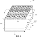
- Figure 1 provides a schematic block view of a detector assembly 100 in accordance with various embodiments
- Figure 2 provides an exploded view of aspects of the detector assembly 100
- Figure 3 provides a sectional view taken along line 3-3 of Figure 1
- the detector assembly 100 includes a semiconductor detector 110, a pinhole collimator 130, and a processing unit 150, which for the clarity of the drawings is shown only in Figure 1 .
- the semiconductor detector 110 produces signals in response to absorption events (e.g., photons produced in response to a radiopharmaceutical that has been administered to an object being imaged that impact the semiconductor detector 110).
- the signals are provided to the processing unit 150, which uses identified events to reconstruct an image of the object being imaged and to derive the location of the event inside the physical pixel as described, for example in US Patent Application Serial No. 15/280640 .
- the pinhole collimator 130 guides photons to the semiconductor detector 110, and limits the angular range of approach of photons to a given pixel or portion of the semiconductor detector 110, helping to allow for accurate determination of the portion of the object being imaged from which a given detected event originated.
- the semiconductor detector 110 has a first surface 112 and a second surface 114.
- the second surface 114 is opposed to the first surface 112 (and, likewise, the first surface 112 is opposed to the second surface 114).
- the semiconductor detector 110 is configured to generate electrical signal in response to photon impacts, and may be made of, for example, Cadmium Zinc Telluride (CZT).
- CZT Cadmium Zinc Telluride
- the second surface 114 includes pixelated anodes 116 disposed thereon, and the first surface 112 includes a cathode electrode 118 disposed thereon.
- the cathode electrode 118 may be a monolithic, or single, cathode.
- the cathode electrode 118 collects an opposite electrical charge of the pixelated anodes 116, and the pixelated anodes 116 are used to generate signals in response to charges generated by the semiconductor detector 110 responsive to photon impacts.
- the pixelated anodes 116 may be arranged in a grid, with the location of one or more pixelated anodes 116 at which a signal is generated responsive to a photon impact used to determine a corresponding location in the object corresponding to the photon impact.
- the pinhole collimator 130 is interposed between the semiconductor detector 110 and an object being imaged (not shown), and is used to control passage of radiation from the object being imaged to the semiconductor detector 110 via the pinhole collimator 130.
- the pinhole collimator 130 guides photons to the semiconductor detector 110, limiting an angular range of approach for photons that impact the semiconductor detector 110.
- the pinhole collimator 130 includes an array 132 of pinhole openings 134 corresponding to the pixelated anodes 116 on the second surface 114.
- the array 132 of pinhole openings 134 has a 1:1 correspondence with an array or grid of pixelated anodes 116, with both the pixelated anodes 116 and array 132 of pinhole openings 134 arranged in an 8 x 8 layout when the projections of openings 132 on the second surface 114 of the detector 110 are centered in the pixelated anodes 116. Accordingly, in the illustrated embodiment, each pinhole opening 134 is associated with a single pixelated anode 116 of the semiconductor detector 110.
- each pinhole opening 134 defines an area, with the area of each pinole opening 134 smaller than a corresponding area of the corresponding pixelated anode 116.
- the width of each pixelated anode 116 is greater than the width of a corresponding pinhole opening 134.
- the pixelated anode 116 and pinhole opening 134 are generally square-shaped, the area of the pixelated anode 116 is greater than the area of the pinhole opening 134. It may be noted that the depicted examples have generally square-shaped cross-sections. Other shapes of opening (e.g., circular, rectangular, or triangular, among others), may be utilized in alternate embodiments.
- the pinhole collimator 130 includes a top plate 140 through which the pinhole openings 134 pass.
- the top plate 140 is mounted to a collimator base 131.
- the pinhole collimator 130 also includes plural septa 142 (or walls) extending along a height of the collimator base 131 that define collimator cells 144 corresonding to the pinhole openings 134.
- each pinhole opening 134 is associated with a particular collimator cell 144 and a particular pixelated anode 116, with photons that pass through the pinhole opening 134 passing through the corresponding collimator cell 144 toward the corresponding pixelated anode 116.
- Each collimator cell 144 defines a cavity between the corresponding pinhole opening 134 and the corresponding pixelated anode 116.
- the septa 142 act to reduce or eliminate passage of a photon through a pinhole opening 134 to non-corresponding pixelated anodes (e.g., pixelated anodes adjacent to the particular pixelated anode that corresponds to the particular pinhole opening).
- a cell width 148 defined by the septa 142 e.g., a width between neighboring septa 142 is greater than an opening width 146 defined by the pinhole openings 134.
- the cell width 148 is 3 times or more greater than the opening width 146.
- the cell width 148 is d, and the opening width 146 is d/3, or the cell width 148 is 3 times greater than the opening width 146. It may be noted that, in contrast, an opening width and width between neighboring walls may be identical for a parallel-hole collimator.
- the septa 142 are parallel to each other and define square-shaped cross sections for each collimator cell 144; however, it may be noted that different configurations may be employed in alternate embodiments.
- the top plate 140 has a thickness 141, and the septa 142 have a thickness 143. In the depicted example, the thickness 141 of the top plate 140 is greater than the thickness 143 of the septa 142.
- the septa 142 are parallel to each other and define square-shaped cross sections for each collimator cell 144; however, it may be noted that different configurations may be employed in alternate embodiments.
- FIG. 4 illustrates a cross-section of an example embodiment of a top plate 400 (e.g., which maybe used as top plate 140) that may be used with pinhole collimator 130 in various embodiments.
- the top plate 400 includes a first surface 402 configured to be positioned proximate a semiconductor detector (e.g., semiconductor detector 110), or oriented toward an interior 410 of a collimator (e.g., pinhole collimator 130) including the top plate 400.
- the top plate 400 also includes a second surface 404 that is opposed to the first surface 402. The second surface 404 is farther away from the semiconductor detector than the first surface 402 is, or the second surface 404 is oriented toward an object 420 being imaged from which photons 422 are emitted.
- the top plate 400 includes pinhole openings 430 through which photons 422 pass toward the semiconductor detector.
- the depicted pinhole openings 430 each have a first width 432 at the first surface 402, and a second width 434 at the second surface 404.
- the first width 432 is greater than the second width 434.
- the pinhole openings 430 are tapered, and are larger at the first surface 402 than at the second surface 404. It may be noted that the taper orientation of the openings 430 in the plate 400 of Figure 4 is opposite to the taper orientation of the openings 134 in the plate 140 of Figures 1-3 .
- the tapered shape in various embodiments is configured to facilitate passage of photons over a preferred or desired angular range.
- FIG. 5 illustrates a cross-section of an example embodiment of pinhole collimator septa 500 that may be used with pinhole collimator 130 in various embodiments.
- Septa 500 include a first surface 502 proximate to a top plate (e.g., top plate 141, top plate 400; top plate not shown in Figure 5 ), and a second surface 504 proximate to a semiconductor detector (e.g., semiconductor detector 110; semiconductor detector not shown in Figure 5 ).
- Cells 506, through which photons pass, are defined between neighboring septa 500.
- the cells 506 are a first width 512 at the first surface 502, and a second width 514 at the second surface 504, with the second width 514 greater than the first width 512.
- a first width 503 of the septa 500 at the first surface 502 is greater than a second width 505 of the septa 500 at the second surface 504.
- a pitch 530 is defined by the septa 500, with the first width 512 less than the pitch 530.
- the tapered septa 500 in various embodiments may cooperate or be complementary with tapered openings (e.g., openings 434).
- the tapered septa 500 may be formed by 3D printing a collimator block.
- the tapered septa 500 provide additional thickness (e.g., relative to septa thickness of a parallel hole collimator) for improved reduction of penetration by photons into adjacent collimator cells.
- the tapered shape in various embodiments is configured to facilitate passage of photons over a preferred or desired angular range. It may be noted that while the description above includes top plate 141 or 400, the pinholes-array collimator of Figure 5 may not include a top plate at all when opening 512 is in the desired size of the pinholes openings such as the size of openings 134 and 434 of Figures 4 and 1-3 , respectively.
- pinhole collimation in various embodiments provides for reduced overlap of solid angles defined by virtual sub-pixels, thereby providing for greater independence of equations defined by the virtual sub-pixels and improved imaging by improving spatial-resolution.
- solid viewing angles defined by virtual sub-pixels 117 via corresponding pinhole openings 134 have less overlapping than solid viewing angles defined by identical virtual sub-pixels via a parallel hole collimator having a sensitivity equal to a sensitivity of the pinhole collimator 130.
- solid angles corresponding to the pinhole collimator 130 may be seen in Figure 3 .
- the solid angles defined by virtual sub-pixels may vary based on a depth (or depths) within the semiconductor detector 110 assigned to events.
- solid angles 320a, 320b, and 320c result from using a common absorption depth (e.g., 1/ ⁇ , where ⁇ is an aborption coefficient) for events from three adjacent virtual sub-pixels 117.
- solid angles 330a, 330b, and 330c result from using varying absorption depths for events from three adjacent virtual sub-pixels 117.
- the cell width 148 between septa 142 of the pinhole collimator equals d
- a height 149 of the pinhole collimator 130 is h/3
- the opening width 146 defined by the pinhole openings 134 is d/3.
- a detector system 600 includes a parallel hole collimator 602 that includes walls 610 having a common opening width 612 therebetween.
- the opening width 612 defines the width of openings 620.
- the detector system 600 also includes a detector unit 621 that includes pixelated anodes 616 having virtual sub-pixels 617 associated therewith (e.g., by a processing unit).
- solid angles 660a, 660b, and 660c result from using a common absorption depth (e.g., at the surface of the detector unit 621) for events from three adjacent virtual sub-pixels 617.
- the solid angles (solid angles 320a, 320b, and 320c and/or solid angles 330a, 330b, and 330c) for the pinhole collimator 130 have noticeably less overlap than the solid angles for parallel hole collimator 602 (solid angles 660a, 660b, and 660c).
- the width 612 between walls (as well as width of openings 620) is d, and the height 652 of the parallel hole collimator 602 is h.
- the sensitivity of a detector system using a collimator corresponds to an aspect ratio defined by the ratio of the width of a collimator opening to the height of the collimator. Accordingly, for the example embodiment illustrated in Figure 3 , the aspect ratio is (d/3)/(h/3), or d/h. Similarly for the parallel hole example of Figure 6 , the aspect ratio is d/h. Accordingly, the collimators of Figure 6 and Figure 3 have identical aspect ratios and provide similar sensitivities; however, the collimator of Figure 3 has a much shorter height (1/3 of the height of the collimator of Figure 6 ).
- the pinhole collimator 130 in various embodiments accordingly provides various benefits when compared to conventional parallel hole collimator arrangements.
- the pinhole collimator 130 provides solid viewing angles that are more tilted and have less overlap than solid viewing angles of a parallel hole collimator, thereby providing better information for reconstruction of an image and resulting in improved spatial resolution.
- the improved spatial resolution capabilities in some embodiments may be used to improve sensitivity while maintaining a same or similar spatial resolution.
- shorter collimator height allows for a more compact detector head, allowing for more detector heads to be used, to provide greater ranges of movement (e.g., rotation) of detector heads, and to reduce or eliminate collisions or interference between neighboring detector heads.
- the processing unit 150 is operably coupled to the semiconductor detector 110, and is configured to identify detected events, deriving the location of events within physical pixels 119 and based on their location, assigning them to virtual sub-pixels 117 distributed along a length 190 and width 191 of the semiconductor detector 110 to be counted there.
- the virtual sub-pixels 117 are represented by dashed lines passing through the semiconductor detector correpsonding to the location of the virtual sub-pixels 117.
- the semiconductor detector 110 includes pixels 119.
- Each pixel 119 may be understood as including a pixelated anode 116, with each pixelated anode 116 smaller (having a smaller area) than the corresponding pixel 119.
- there are 9 virtual sub-pixels 117 per pixelated anode 116 or pixel 119 e.g., a grid of 3 x 3 virtual sub-pixels 117 per pixelated anode 116 or pixel 119).
- Each pixel 119 includes a plurality of corresponding virtual sub-pixels, with absorbed photons in the semiconductor detector 110 counted as events in a corresponding virtual sub-pixel.
- the processing unit 150 includes processing circuitry configured to perform one or more tasks, functions, or steps discussed herein. It may be noted that "processing unit” as used herein is not intended to necessarily be limited to a single processor or computer. For example, the processing unit 150 may include multiple processors, ASIC's, FPGA's, and/or computers, which may be integrated in a common housing or unit, or which may distributed among various units or housings. It may be noted that operations performed by the processing unit 150 (e.g., operations corresponding to process flows or methods discussed herein, or aspects thereof) may be sufficiently complex that the operations may not be performed by a human being within a reasonable time period. For example, the determination of values of collected, non-collected, and/or combined charge signals within the time constraints associated with such signals may rely on or utilize computations that may not be completed by a person within a reasonable time period.
- signals are generated by one or more pixelated anodes 116 in response to a photon impact, with the location of the pixelated anode(s) 116 generating a signal used to determine a corresponding location in the object for which an event is counted.
- signals from adjacent pixels may be used to assign a virtual sub-pixel location within a given pixelated anode 116.
- the processing unit 150 is configured to determine an absorption location for a given absorbed phon based on non-collected signals received from pixelated anodes adjancent to a pixelated anode abosrobing the given absorbed photon.
- virtual pixels may be employed along a thickness of the semiconductor detector 110.
- Virtual pixels employed along a thickness of the semiconductor detector 110 may be used to represent different depths of absorption of photons.
- the semiconductor detector 110 has a thickness 396. Three rows of virtual pixels are distributed along the thickness 396 - a first row 390, a second row 392, and a third row 394.
- the processing unit 150 in various embodiments is configured to identify detector events with the virtual sub-pixels in the first row 390, second row 392, and third row 394 distributed alogn the thickness 396.
- different virtual sub-pixels along a thickness may be used to provide different absorption depths for identifying event locations.
- event 331a is shown at a depth corresponding to the first row 390
- event 331b is shown at a depth corresponding to the third row 394
- event 331c is shown at a depth corresponding to the second row 392.
- the processing unit 150 is configured to count absorbed photons as events within the thickness 396 of the semiconductor detector 110 at a location (e.g., a distance from the cathode 118) corresponding to one over an absorption coefficient of the semiconductor detector 110.
- photons e.g., photons at a given energy corresponding with the absorption coefficient
- photons may be counted as events at a location in the semiconductor detector a distance 395 from the second surface 112 (and/or cathode 118) along the thickness 396, as shown for event locations 321a, 321b, and 321c of Figure 3 .
- the distance 395 in various embodiments is 1/ ⁇ . It may be noted that ⁇ may vary based on photon energy.
- absorption location for each photon is defined within a range of 1/ ⁇ ⁇ 1 millimeter.
- the processing unit 150 is configured to count absorbed photons as events within the thickness 396 of the semiconductor detector 110 at a distance corresponding to an energy window width used to identify the events as photon impacts.
- the energy window width in various embodiments is a range of energies around the photopeak energy which are considered as true events.
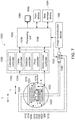
- FIG 7 is a schematic illustration of a NM imaging system 1000 having a plurality of imaging detector head assemblies mounted on a gantry (which may be mounted, for example, in rows, in an iris shape, or other configurations, such as a configuration in which the movable detector carriers 1016 are aligned radialy toward the patient-body 1010).
- a plurality of imaging detectors 1002 are mounted to a gantry 1004.
- Each detector 1002 may include, for example, collimators and detectors arranged generally similarly to the arrangements discussed in connection with Figures 1-6 .
- the imaging detectors 1002 are configured as two separate detector arrays 1006 and 1008 coupled to the gantry 1004 above and below a subject 1010 (e.g., a patient), as viewed in Figure 7 .
- the detector arrays 1006 and 1008 may be coupled directly to the gantry 1004, or may be coupled via support members 1012 to the gantry 1004 to allow movement of the entire arrays 1006 and/or 1008 relative to the gantry 1004 (e.g., transverse translating movement in the left or right direction as viewed by arrow T in Figure 7 ).
- each of the imaging detectors 1002 includes a detector unit 1014 (which may include collimator and/or detector assemblies as discussed herein in connection with Figures 1-6 ), at least some of which are mounted to a movable detector carrier 1016 (e.g., a support arm or actuator that may be driven by a motor to cause movement thereof) that extends from the gantry 1004.
- a movable detector carrier 1016 e.g., a support arm or actuator that may be driven by a motor to cause movement thereof
- the detector carriers 1016 allow movement of the detector units 1014 towards and away from the subject 1010, such as linearly.
- the detector arrays 1006 and 1008 are mounted in parallel above and below the subject 1010 and allow linear movement of the detector units 1014 in one direction (indicated by the arrow L), illustrated as perpendicular to the support member 1012 (that are coupled generally horizontally on the gantry 1004).
- the movable detector carrier 1016 may be any type of support that allows movement of the detector units 1014 relative to the support member 1012 and/or gantry 1004, which in various embodiments allows the detector units 1014 to move linearly towards and away from the support member 1012.
- Each of the imaging detectors 1002 in various embodiments is smaller than a conventional whole body or general purpose imaging detector.
- a conventional imaging detector may be large enough to image most or all of a width of a patient's body at one time and may have a diameter or a larger dimension of approximately 50 cm or more.
- each of the imaging detectors 1002 may include one or more detector units 1014 coupled to a respective detector carrier 1016 and having dimensions of, for example, 4 cm to 20 cm and may be formed of Cadmium Zinc Telluride (CZT) tiles or modules.
- CZT Cadmium Zinc Telluride
- each of the detector units 1014 may be 8x8 cm in size and be composed of a plurality of CZT pixelated modules (not shown).
- each detector unit 1014 includes a plurality of modules, such as an array of 1 x 7 modules. However, different configurations and array sizes are contemplated including, for example, detector units 1014 having multiple rows of modules.
- imaging detectors 1002 may be different sizes and/or shapes with respect to each other, such as square, rectangular, circular or other shape.
- An actual field of view (FOV) of each of the imaging detectors 1002 maybe directly proportional to the size and shape of the respective imaging detector.
- the gantry 1004 may be formed with an aperture 1018 (e.g., opening or bore) therethrough as illustrated.
- a patient table 1020 such as a patient bed, is configured with a support mechanism (not shown) to support and carry the subject 1010 in one or more of a plurality of viewing positions within the aperture 1018 and relative to the imaging detectors 1002.
- the gantry 1004 may comprise a plurality of gantry segments (not shown), each of which may independently move a support member 1012 or one or more of the imaging detectors 1002.
- the gantry 1004 may also be configured in other shapes, such as a "C", “H” and “L”, for example, and may be rotatable about the subject 1010.
- the gantry 1004 may be formed as a closed ring or circle, or as an open arc or arch which allows the subject 1010 to be easily accessed while imaging and facilitates loading and unloading of the subject 1010, as well as reducing claustrophobia in some subjects 1010.
- Additional imaging detectors may be positioned to form rows of detector arrays or an arc or ring around the subject 1010.
- image data specific for a larger FOV may be acquired more quickly.
- Each of the imaging detectors 1002 has a radiation detection face, which is directed towards the subject 1010 or a region of interest within the subject.
- multi-bore collimators may be constructed to be registered with pixels of the detector units 1014, which in one embodiment are CZT detectors. However, other materials may be used.
- Registered collimation may improve spatial resolution by forcing photons going through one bore to be collected primarily by one pixel. Additionally, registered collimation may improve sensitivity and energy response of pixelated detectors as detector area near the edges of a pixel or in-between two adjacent pixels may have reduced sensitivity or decreased energy resolution or other performance degradation. Having collimator septa directly above the edges of pixels reduces the chance of a photon impinging at these degraded-performance locations, without decreasing the overall probability of a photon passing through the collimator. As discussed herein, in various embodiments parallel-hole and/or pin-hole collimation may be employed.
- a controller unit 1030 may control the movement and positioning of the patient table 1020, imaging detectors 1002 (which maybe configured as one or more arms), gantry 1004 and/or the collimators 1022 (that move with the imaging detectors 1002 in various embodiments, being coupled thereto).
- a range of motion before or during an acquisition, or between different image acquisitions, is set to maintain the actual FOV of each of the imaging detectors 1002 directed, for example, towards or "aimed at" a particular area or region of the subject 1010 or along the entire subject 1010.
- the motion may be a combined or complex motion in multiple directions simultaneously, concurrently, or sequentially as described in more detail herein.
- the controller unit 1030 may have a gantry motor controller 1032, table controller 1034, detector controller 1036, pivot controller 1038, and collimator controller 1040.
- the controllers 1030, 1032, 1034, 1036, 1038, 1040 may be automatically commanded by a processing unit 1050, manually controlled by an operator, or a combination thereof.
- the gantry motor controller 1032 may move the imaging detectors 1002 with respect to the subject 1010, for example, individually, in segments or subsets, or simultaneously in a fixed relationship to one another.
- the gantry controller 1032 may cause the imaging detectors 1002 and/or support members 1012 to move relative to or rotate about the subject 1010, which may include motion of less than or up to 180 degrees (or more).
- the table controller 1034 may move the patient table 1020 to position the subject 1010 relative to the imaging detectors 1002.
- the patient table 1020 maybe moved in up-down directions, in-out directions, and right-left directions, for example.
- the detector controller 1036 may control movement of each of the imaging detectors 1002 to move together as a group or individually as described in more detail herein.
- the detector controller 1036 also may control movement of the imaging detectors 1002 in some embodiments to move closer to and farther from a surface of the subject 1010, such as by controlling translating movement of the detector carriers 1016 linearly towards or away from the subject 1010 (e.g., sliding or telescoping movement).
- the detector controller 1036 may control movement of the detector carriers 1016 to allow movement of the detector array 1006 or 1008.
- the detector controller 1036 may control lateral movement of the detector carriers 1016 illustrated by the T arrow (and shown as left and right as viewed in Figure 7 ). In various embodiments, the detector controller 1036 may control the detector carriers 1016 or the support members 1012 to move in different lateral directions. Detector controller 1036 may control the swiveling motion of detectors 1002 together with their collimators 1022.
- the pivot controller 1038 may control pivoting or rotating movement of the detector units 1014 at ends of the detector carriers 1016 and/or pivoting or rotating movement of the detector carrier 1016.
- one or more of the detector units 1014 or detector carriers 1016 maybe rotated about at least one axis to view the subject 1010 from a plurality of angular orientations to acquire, for example, 3D image data in a 3D SPECT or 3D imaging mode of operation.
- the collimator controller 1040 may adjust a position of an adjustable collimator, such as a collimator with adjustable strips (or vanes) or adjustable pinhole(s).
- motion of one or more imaging detectors 1002 may be in directions other than strictly axially or radially, and motions in several motion directions may be used in various embodiment. Therefore, the term "motion controller" may be used to indicate a collective name for all motion controllers. It should be noted that the various controllers may be combined, for example, the detector controller 1036 and pivot controller 1038 may be combined to provide the different movements described herein.
- the imaging detectors 1002, gantry 1004, patient table 1020 and/or collimators 1022 may be adjusted, such as to first or initial imaging positions, as well as subsequent imaging positions.
- the imaging detectors 1002 may each be positioned to image a portion of the subject 1010.
- one or more of the imaging detectors 1002 may not be used to acquire data, such as the imaging detectors 1002 at ends of the detector arrays 1006 and 1008, which as illustrated in Figure 7 are in a retracted position away from the subject 1010.
- Positioning may be accomplished manually by the operator and/or automatically, which may include using, for example, image information such as other images acquired before the current acquisition, such as by another imaging modality such as X-ray Computed Tomography (CT), MRI, X-Ray, PET or ultrasound.
- CT computed Tomography
- the additional information for positioning, such as the other images may be acquired by the same system, such as in a hybrid system (e.g., a SPECT/CT system).
- the detector units 1014 may be configured to acquire non-NM data, such as x-ray CT data.
- a multi-modality imaging system may be provided, for example, to allow performing NM or SPECT imaging, as well as x-ray CT imaging, which may include a dual-modality or gantry design as described in more detail herein.
- one or more images such as three-dimensional (3D) SPECT images are acquired using one or more of the imaging detectors 1002, which may include using a combined motion that reduces or minimizes spacing between detector units 1014.
- the image data acquired by each imaging detector 1002 may be combined and reconstructed into a composite image or 3D images in various embodiments.
- At least one of detector arrays 1006 and/or 1008, gantry 1004, patient table 1020, and/or collimators 1022 are moved after being initially positioned, which includes individual movement of one or more of the detector units 1014 (e.g., combined lateral and pivoting movement) together with the swiveling motion of detectors 1002.
- at least one of detector arrays 1006 and/or 1008 maybe moved laterally while pivoted.
- a plurality of small sized detectors, such as the detector units 1014 maybe used for 3D imaging, such as when moving or sweeping the detector units 1014 in combination with other movements.
- a data acquisition system (DAS) 1060 receives electrical signal data produced by the imaging detectors 1002 and converts this data into digital signals for subsequent processing. However, in various embodiments, digital signals are generated by the imaging detectors 1002.
- An image reconstruction device 1062 (which may be a processing device or computer) and a data storage device 1064 may be provided in addition to the processing unit 1050. It should be noted that one or more functions related to one or more of data acquisition, motion control, data processing and image reconstruction may be accomplished through hardware, software and/or by shared processing resources, which may be located within or near the imaging system 1000, or may be located remotely.
- a user input device 1066 may be provided to receive user inputs (e.g., control commands), as well as a display 1068 for displaying images.
- DAS 1060 receives the acquired images from detectors 1002 together with the corresponding lateral, vertical, rotational and swiveling coordinates of gantry 1004, support members 1012, detector units 1014, detector carriers 1016, and detectors 1002 for accurate reconstruction of an image including 3D images and their slices.
- Figure 8 illustrates a detector assembly that is similar to the detector assembly illustrated by Figure 3 with the exception that the virtual sub-pixels of Figure 8 are arranged in one layer along a Z direction.
- Figure 8 specifically refers to collimator cells 2000, with each collimator cell_confining a single pixel 119 (and corresponding pixelated anode 116), and includes a single pinhole 134.
- Each physical pixel 119 has size P that is equal to the pitch of the pixels 116, pinholes 134 and cells 2000.
- Each pixel 119 is divided into multiple virtual sub-pixels 2002.
- Figure 8 shows viewing angles 2004 as observed from virtual sub-pixels 2002 via pinholes 134 to the object being imaged (not shown). Each viewing angle 2004 belong to a different cell 2000.
- each virtual pixel 2002 corresponding to viewing angle 2004 and pinhole 134 is the same. Accordingly all the viewing angles 2004 form the same angle ⁇ with the first surface 112 and thus, are parallel to each other and are displaced from each other by a distance that is equal to the pitch of pixels 119 and pinholes 134.
- the discussion about the system (detector assembly 100) spatial-resolution will be divided into two steps: The first step analyzes the system spatial-resolution for a single cell 2000 and the second step analyzes the system-spatial resolution for an array of multiple cells 2000 closely packed and butted together into a matrix of cells (collimator 130) that each of them includes a single pinhole 134 and confines a single pixels 116.
- R s is the system spatial-resolution
- R c is the collimator (cell 2000) spatial-resolution
- d is distance 148 between the walls of cells 2000
- d/3 is the opening size of pinhole 134
- h/3 is the the height of collimator 130
- b is the distance from collimator 130 to the object being imaged (not shown)
- r i is the intrinsic resolution of virtual sub-pixels 2002 and is equal to the size of virtual sub-pixels 2002
- collimator 130 including multiple cells 2000
- parallel viewing angles 2004 are displaced from each other by a distance P, which defines the intrinsic resolution in parallel collimation.
- the system spatial-resolution is the smaller value derived either from Equation (1) or Equation (2).
- the magnification M b / (h/3) that appears in Equation (1) is the ratio between the distance b from the collimator to the imaged object and the collimator height (h/3).
- M is large. Accordingly, the value of the system spatial-resolution according to Equation (1) may be larger than the one according to Equation (2), and then the system spatial-resolution is determined by Equation (2).
- M is small, and, accordingly, the value of the system spatial-resolution according to Equation (1) may be smaller than the one according to Equation (2) and then the system spatial-resolution is determined by Equation (1).
- the system spatial-resolution of pinhole collimator 130 in accordance with various embodiments herein is the smaller of the system spatial-resolution as derived either by Equations (1) or (2).
- the system spatial-resolution according to various embodiments is better than this of a parallel hole collimator.
- P is smaller than the term r i x M.
- the system spatial-resolution according to the embodiments of the invention is better than this of a conventional pinhole collimator.
- the various embodiments may be implemented in hardware, software or a combination thereof.
- the various embodiments and/or components also may be implemented as part of one or more computers or processors.
- the computer or processor may include a computing device, an input device, a display unit and an interface, for example, for accessing the Internet.
- the computer or processor may include a microprocessor.
- the microprocessor may be connected to a communication bus.
- the computer or processor may also include a memory.
- the memory may include Random Access Memory (RAM) and Read Only Memory (ROM).
- the computer or processor further may include a storage device, which may be a hard disk drive or a removable storage drive such as a solid-state drive, optical disk drive, and the like.
- the storage device may also be other similar means for loading computer programs or other instructions into the computer or processor.
- the term "computer” or “module” may include any processor-based or microprocessor-based system including systems using microcontrollers, reduced instruction set computers (RISC), ASICs, logic circuits, and any other circuit or processor capable of executing the functions described herein.
- RISC reduced instruction set computers
- ASIC application specific integrated circuit
- logic circuits logic circuits, and any other circuit or processor capable of executing the functions described herein.
- the above examples are exemplary only, and are thus not intended to limit in any way the definition and/or meaning of the term "computer”.
- the computer or processor executes a set of instructions that are stored in one or more storage elements, in order to process input data.
- the storage elements may also store data or other information as desired or needed.
- the storage element may be in the form of an information source or a physical memory element within a processing machine.
- the set of instructions may include various commands that instruct the computer or processor as a processing machine to perform specific operations such as the methods and processes of the various embodiments.
- the set of instructions may be in the form of a software program.
- the software may be in various forms such as system software or application software and which may be embodied as a tangible and non-transitory computer readable medium. Further, the software may be in the form of a collection of separate programs or modules, a program module within a larger program or a portion of a program module.
- the software also may include modular programming in the form of object-oriented programming.
- the processing of input data by the processing machine may be in response to operator commands, or in response to results of previous processing, or in response to a request made by another processing machine.
- a structure, limitation, or element that is “configured to” perform a task or operation is particularly structurally formed, constructed, or adapted in a manner corresponding to the task or operation.
- an object that is merely capable of being modified to perform the task or operation is not “configured to” perform the task or operation as used herein.
- the use of "configured to” as used herein denotes structural adaptations or characteristics, and denotes structural requirements of any structure, limitation, or element that is described as being “configured to” perform the task or operation.
- a processing unit, processor, or computer that is "configured to" perform a task or operation may be understood as being particularly structured to perform the task or operation (e.g., having one or more programs or instructions stored thereon or used in conjunction therewith tailored or intended to perform the task or operation, and/or having an arrangement of processing circuitry tailored or intended to perform the task or operation).
- a general purpose computer which may become “configured to” perform the task or operation if appropriately programmed) is not “configured to” perform a task or operation unless or until specifically programmed or structurally modified to perform the task or operation.
- the terms "software” and “firmware” are interchangeable, and include any computer program stored in memory for execution by a computer, including RAM memory, ROM memory, EPROM memory, EEPROM memory, and nonvolatile RAM (NVRAM) memory.
- RAM memory random access memory
- ROM memory read-only memory
- EPROM memory erasable programmable read-only memory
- EEPROM memory electrically erasable programmable read-only memory
- NVRAM nonvolatile RAM
Abstract
Description
- The subject matter disclosed herein relates generally to apparatus and methods for diagnostic medical imaging, such as Nuclear Medicine (NM) imaging.
- In NM imaging, systems with multiple detectors or detector heads may be used to image a subject, such as to scan a region of interest. For example, the detectors may be positioned adjacent the subject to acquire NM data, which is used to generate a three-dimensional (3D) image of the subject.
- Single Photon Emission Computed Tomography (SPECT) systems may have moving detector heads, such as gamma detectors positioned to focus on a region of interest. For example, a number of gamma cameras may be moved (e.g., rotated) to different angular positions for acquiring image data. The acquired image data is then used to generate the 3D images.
- The size of the detector heads may limit an available usable area for the placement of detectors, such as Cadmium Zinc Telluride (CZT) wafers. The sensitivity (e.g., the proportion of radiation received relative to the radiation emitted) may be limited by the size of the detector heads and/or the arrangement of CZT wafers. Conventional approaches to improving sensitivity may use thicker detectors, or detectors arranged in generally identical or similar layers stacked directly one on top of each other. Such conventional approaches may not provide a desired or required sensitivity.
- In one embodiment, a detector assembly is provided that includes a semiconductor detector, a pinhole collimator, and a processing unit. The semiconductor detector has a first surface and a second surface opposed to each other. The first surface includes pixels, and the second surface includes a cathode electrode. The pinhole collimator includes an array of pinhole openings corresponding to the pixels. Each pinhole opening is associated with a single pixel of the semiconductor detector, and the area of each pinhole opening is smaller than a corresponding area of the corresponding pixel, which is exposed to radiation. (It may be noted that the pixel area less the radiation blocking area of the collimator immediately above the pixel is exposed to radiation in some embodiments). The processing unit is operably coupled to the semiconductor detector and configured to identify detected events within virtual sub-pixels distributed along a length and width of the semiconductor detector. Each pixel includes (e.g., has associated therewith) a plurality of corresponding virtual sub-pixels (as interpreted by the processing unit), wherein absorbed photons are counted as events in a corresponding virtual sub-pixel.
- In another embodiment, a detector assembly is provided that includes a semiconductor detector, a collimator, and a processing unit. The semiconductor detector has a first surface and a second surface opposed to each other. The first surface includes pixels (which in turn comprise corresponding pixelated anodes), and the second surface includes a cathode electrode. The collimator includes openings. Each opening is associated with a single corresponding pixelated anode of the semiconductor detector. The processing unit is configured to identify detected events within virtual sub-pixels distributed along a length and width of the semiconductor detector. Each pixel includes (e.g., has associated therewith) a plurality of corresponding virtual sub-pixels. Absorbed photons are counted as events in a corresponding virtual sub-pixel, with absorbed photons counted as events within a thickness of the semiconductor detector at a distance corresponding to one over an absorption coefficient of the detector.
- In another embodiment, a detector assembly includes a semiconductor detector, a collimator and a processing unit. The semiconductor detector has a first surface and a second surface opposed to each other. The first surface includes pixels (which in turn comprise corresponding pixelated anodes), and the second surface includes a cathode electrode. The collimator includes openings, with each opening associated with a single corresponding pixel of the semiconductor detector. The processing unit is configured to identify detected events within virtual sub-pixels distributed along a length and width of the semiconductor detector. Each pixel includes (e.g., has associated therewith) a plurality of corresponding virtual sub-pixels, with absorbed photons are counted as events in a corresponding virtual sub-pixel. Absorbed photons are counted as events within a thickness of the semiconductor detector at a distance corresponding to an energy window width used to identify the events as photon impacts.
- In the drawings:
-
Figure 1 provides a schematic block view of a detector assembly in accordance with various embodiments. -
Figure 2 provides an exploded view of aspects of the detector assembly ofFigure 1 . -
Figure 3 provides a sectional view taken along line 3-3 ofFigure 1 . -
Figure 4 illustrates a cross-section of a top plate formed in accordance with various embodiments. -
Figure 5 illustrates a cross-section of pinhole collimator septa in accordance with various embodiments. -
Figure 6 depicts examples of solid angles corresponding to use of a parallel hole collimator. -
Figure 7 is a schematic block diagram of a Nuclear Medicine (NM) imaging system in accordance with various embodiments. -
Figure 8 schematically shows parallel viewing angles of virtual sub-pixels in a configuration of detector assembly that is similar toFigure 3 but has one layer of virtual sub-pixels in a Z direction. - The following detailed description of certain embodiments will be better understood when read in conjunction with the appended drawings. To the extent that the figures illustrate diagrams of the functional blocks of various embodiments, the functional blocks are not necessarily indicative of the division between hardware circuitry. For example, one or more of the functional blocks (e.g., processors or memories) may be implemented in a single piece of hardware (e.g., a general purpose signal processor or a block of random access memory, hard disk, or the like) or multiple pieces of hardware. Similarly, the programs may be stand alone programs, may be incorporated as subroutines in an operating system, may be functions in an installed software package, and the like. It should be understood that the various embodiments are not limited to the arrangements and instrumentality shown in the drawings.
- As used herein, the terms "system," "unit," or "module" may include a hardware and/or software system that operates to perform one or more functions. For example, a module, unit, or system may include a computer processor, controller, or other logic-based device that performs operations based on instructions stored on a tangible and non-transitory computer readable storage medium, such as a computer memory. Alternatively, a module, unit, or system may include a hard-wired device that performs operations based on hard-wired logic of the device. Various modules or units shown in the attached figures may represent the hardware that operates based on software or hardwired instructions, the software that directs hardware to perform the operations, or a combination thereof.
- "Systems," "units," or "modules" may include or represent hardware and associated instructions (e.g., software stored on a tangible and non-transitory computer readable storage medium, such as a computer hard drive, ROM, RAM, or the like) that perform one or more operations described herein. The hardware may include electronic circuits that include and/or are connected to one or more logic-based devices, such as microprocessors, processors, controllers, or the like. These devices may be off-the-shelf devices that are appropriately programmed or instructed to perform operations described herein from the instructions described above. Additionally or alternatively, one or more of these devices may be hard-wired with logic circuits to perform these operations.
- As used herein, an element or step recited in the singular and preceded with the word "a" or "an" should be understood as not excluding plural of said elements or steps, unless such exclusion is explicitly stated. Furthermore, references to "one embodiment" of are not intended to be interpreted as excluding the existence of additional embodiments that also incorporate the recited features. Moreover, unless explicitly stated to the contrary, embodiments "comprising" or "having" an element or a plurality of elements having a particular property may include additional elements not having that property.
- Various embodiments provide systems and methods for improving the sensitivity of image acquisition, for example in Nuclear Medicine (NM) imaging applications. Various embodiments provide one or more different approaches for improving sensitivity and/or other aspects of detector performance. For example, in one approach, an array of pinhole openings are used in a collimator for a detector system. As another example, additionally or alternatively, in a second approach, all events are identified as being absorbed at a location and/or within a range corresponding to an absorption coefficient of the detector (e.g., one over the absorption coefficient of the detector). As one more example, in a third approach, all events are identified as being absorbed at a location and/or within a range that ensures that the energy of the events is measured within the energy window used for imaging. It may be noted that each of the three approaches discussed above in this paragraph may be employed with the use of virtual sub-pixels (or virtual division of the detector) along X and Y directions (or along the width and length of the detector).
- In various embodiments, a pinhole collimator includes an array of pinholes that defines multiples cells. Each cell includes or corresponds to only a single physical pixel of the detector and only a single pinhole of the array. In various embodiments, in contrast to certain conventional approaches, radiation from a given pinhole (also referred to herein as a pinhole opening) only arrives at one particular physical pixel corresponding to the given pinhole. It may be noted that the physical pixel may be viewed as including a number of virtual sub-pixels by a processing unit. Each event detected in the physical pixel is counted as related to one of the virtual sub-pixels into which the physical pixel is divided to. The virtual sub-pixel to which the event belongs to is determined by the location of the event within the physical pixel that includes the virtual sub-pixels. There are known methods to derive the location of the event within the physical pixel, such as the method described in
US Patent application No. 15/280640 Figure 8 . virtual sub-pixels - Further, use of a pinhole array instead of a parallel hole array in various embodiments provides for a smaller area of opening that collects radiation. For example, the size of a pinhole opening may be 1/3 of the width (or 1/9 of the area) of a pixel, whereas an opening of a parallel hole array may be the pixel size less the septa thickness. Accordingly, the opening size in a parallel hole array may be dictated by the pixel size and wall (or septa) thickness; however, in various embodiments employing a pinhole array, the opening size may be selected as desired (e.g., to provide a desired sensitivity and/or collimator height). For example, for the same sensitivity as a parallel hole collimator, an opening size for a pinhole array may be selected to provide a desired height (e.g., 1/3 of the height of a comparable parallel hole array). Additionally, in various embodiments, thicker septa may be used for a pinhole array in comparison to a parallel hole array. In some embodiments, physical pixels may be divided in multiple virtual sub-pixels (e.g., an associated processing unit may assign virtual sub-pixels to each physical pixel) along X and Y directions (or length and width of a detector), while having a single layer in the Z direction (or thickness). Alternatively, in other embodiments, multiple virtual sub-pixels may be employed along the Z direction (or thickness).
- Accordingly, various embodiments provide flexibility to selected collimator height while maintaining a desired sensitivity, by adjusting the size of the openings of a pinhole array, regardless of pixel size or pitch. Such flexibility is especially advantageous when using a collimator within a swiveling detector head. For example, the collimator height may dictate or influence the radius reserved for each head for swiveling motion. The shorter the collimator is, the smaller is the required radius. Accordingly, for a shorter collimator provided by a pinhole array, more heads may be placed around the object being imaged providing improved sensitivity and image quality in comparison with a taller parallel hole collimator. Additionally, the collimator openings produce solid angles through which the virtual pixels observe the object being imaged, with the smaller size of the pinhole openings providing larger and more separated solid angles for the virtual sub-pixels, with less overlap between the solid angles for the virtual sub-pixels of a physical pixel. Accordingly, the use of such pinhole openings improves spatial resolution, or may be used to maintain a desired resolution with a shorter collimator to increase sensitivity and improve image quality. Further, still, the use of thicker septa or walls helps prevent radiation penetriation from a given collimator opening to non-associated pixels (or pixels other than a pixel immediately below the opening), thereby improving image quality. Further still, it may be noted that use of many sub-voxels over the thickness of a detector may reduce the number of events for each volume of interest, thereby increasing statistical noise and degrading image quality. In various embodiments, using only one location (or range) or layer along the Z direction (or thickness) reduces statistical noise and improves image quality.
- It may be noted that in some embodiments, in connection with sub-pixelization along the X and Y directions, a single Z layer, location, or range may be used to identify events along a thickness of a detector. For example, a Z position-range for all events may be defined at or around an average absorption depth of 1/µ, where µ is the absorption coefficient for a specific photon energy for a particular detector material. For example, events may be distributed linearly, as one example, or exponentially, as another example, within a range centered about or otherwise corresponding to distance of 1/µ from the cathode. As another example, a Z position-range for all events may be defined within a range corresponding to energies of the energy window used for imaging. For example, in some embodiments, an absorption location for each absorbed photon within the thickness of the semiconductor detector is defined within a range such that ΔL/D = ΔE/E, where ΔL is a distance from the cathode, D is the detector thickness, ΔE is an energy window width, and E is a photopeak energy of an absorbed photon. Again, the events may be distributed linearly, as one example, or exponentially, as another example. In various embodiments, use of such Z position-ranges (in contrast, for example, to multiple virtual sub-pixels along a detector thickness) helps to reduce statistical noise and to improve image quality. Also, it may be noted that use of such Z position-ranges may be accomplished with simpler hardwarde or software (in compariston to, for example, use of multiple virtual sub-pixels along a detector thickness), providing for easier implementation and/or lower cost.
- A technical effect provided by various embodiments includes increased sensitivity of a detector system, such as a NM imaging detector system. The detector system may be provided in a rotating head detector module that may be used as part of a group of similar rotating head detector modules in an imaging system. A technical effect of various embodiments includes improved image quality and spatial resolution. A technical effect of various embodiments includes reduced collimator height allowing for less room needed to allow a detector head to pivot, allowing more detector heads to be placed closely to an object being imaged. A technical effect of various embodiments includes reduced penetration by radiation to pixels other than a pixel associated with (e.g., located directly below) a collimator opening. A technical effect of various embodiments included reduced statistical noise.
-
Figure 1 provides a schematic block view of adetector assembly 100 in accordance with various embodiments,Figure 2 provides an exploded view of aspects of thedetector assembly 100, andFigure 3 provides a sectional view taken along line 3-3 ofFigure 1 . As seen inFigures 1-3 , thedetector assembly 100 includes asemiconductor detector 110, apinhole collimator 130, and aprocessing unit 150, which for the clarity of the drawings is shown only inFigure 1 . Generally, thesemiconductor detector 110 produces signals in response to absorption events (e.g., photons produced in response to a radiopharmaceutical that has been administered to an object being imaged that impact the semiconductor detector 110). The signals are provided to theprocessing unit 150, which uses identified events to reconstruct an image of the object being imaged and to derive the location of the event inside the physical pixel as described, for example inUS Patent Application Serial No. 15/280640 . Thepinhole collimator 130 guides photons to thesemiconductor detector 110, and limits the angular range of approach of photons to a given pixel or portion of thesemiconductor detector 110, helping to allow for accurate determination of the portion of the object being imaged from which a given detected event originated. - As best seen in
Figure 3 , thesemiconductor detector 110 has afirst surface 112 and asecond surface 114. Thesecond surface 114 is opposed to the first surface 112 (and, likewise, thefirst surface 112 is opposed to the second surface 114). Thesemiconductor detector 110 is configured to generate electrical signal in response to photon impacts, and may be made of, for example, Cadmium Zinc Telluride (CZT). Thesecond surface 114 includespixelated anodes 116 disposed thereon, and thefirst surface 112 includes acathode electrode 118 disposed thereon. In some embodiments, thecathode electrode 118 may be a monolithic, or single, cathode. Thecathode electrode 118 collects an opposite electrical charge of thepixelated anodes 116, and thepixelated anodes 116 are used to generate signals in response to charges generated by thesemiconductor detector 110 responsive to photon impacts. Thepixelated anodes 116 may be arranged in a grid, with the location of one or morepixelated anodes 116 at which a signal is generated responsive to a photon impact used to determine a corresponding location in the object corresponding to the photon impact. - As seen in
Figures 1-3 , thepinhole collimator 130 is interposed between thesemiconductor detector 110 and an object being imaged (not shown), and is used to control passage of radiation from the object being imaged to thesemiconductor detector 110 via thepinhole collimator 130. For example, thepinhole collimator 130 guides photons to thesemiconductor detector 110, limiting an angular range of approach for photons that impact thesemiconductor detector 110. Thepinhole collimator 130 includes anarray 132 ofpinhole openings 134 corresponding to thepixelated anodes 116 on thesecond surface 114. In the illustrated embodiment, thearray 132 ofpinhole openings 134 has a 1:1 correspondence with an array or grid ofpixelated anodes 116, with both thepixelated anodes 116 andarray 132 ofpinhole openings 134 arranged in an 8 x 8 layout when the projections ofopenings 132 on thesecond surface 114 of thedetector 110 are centered in thepixelated anodes 116. Accordingly, in the illustrated embodiment, eachpinhole opening 134 is associated with a singlepixelated anode 116 of thesemiconductor detector 110. Accordingly, radiation that passes through a givenpinhole opening 134 is confined within a single cell ofcollimator 130 and is absorbed at a location corresponding to one and only onepixelated anode 116 that is associated with the given pinhole opening 134 (e.g., located directly beneath the pinhole opening 134). Further, eachpinhole opening 134 defines an area, with the area of eachpinole opening 134 smaller than a corresponding area of the correspondingpixelated anode 116. For example, as seen inFigure 3 , the width of eachpixelated anode 116 is greater than the width of acorresponding pinhole opening 134. Accordingly, if thepixelated anode 116 andpinhole opening 134 are generally square-shaped, the area of thepixelated anode 116 is greater than the area of thepinhole opening 134. It may be noted that the depicted examples have generally square-shaped cross-sections. Other shapes of opening (e.g., circular, rectangular, or triangular, among others), may be utilized in alternate embodiments. - As best seen in
Figures 1 and3 , in various embodiments thepinhole collimator 130 includes atop plate 140 through which thepinhole openings 134 pass. Thetop plate 140 is mounted to acollimator base 131. Thepinhole collimator 130 also includes plural septa 142 (or walls) extending along a height of thecollimator base 131 that definecollimator cells 144 corresonding to thepinhole openings 134. In the illustrated embodiment, eachpinhole opening 134 is associated with aparticular collimator cell 144 and a particularpixelated anode 116, with photons that pass through thepinhole opening 134 passing through the correspondingcollimator cell 144 toward the correspondingpixelated anode 116. Eachcollimator cell 144 defines a cavity between the corresponding pinhole opening 134 and the correspondingpixelated anode 116. Thesepta 142 act to reduce or eliminate passage of a photon through apinhole opening 134 to non-corresponding pixelated anodes (e.g., pixelated anodes adjacent to the particular pixelated anode that corresponds to the particular pinhole opening). Acell width 148 defined by the septa 142 (e.g., a width between neighboring septa 142) is greater than anopening width 146 defined by thepinhole openings 134. For example, in some embodiments, thecell width 148 is 3 times or more greater than theopening width 146. In the example illustrated inFigure 1 to 3 , thecell width 148 is d, and theopening width 146 is d/3, or thecell width 148 is 3 times greater than theopening width 146. It may be noted that, in contrast, an opening width and width between neighboring walls may be identical for a parallel-hole collimator. - In the example illustrated in
Figures 1 to 3 , thesepta 142 are parallel to each other and define square-shaped cross sections for eachcollimator cell 144; however, it may be noted that different configurations may be employed in alternate embodiments. As best seen inFigures 2 and3 , thetop plate 140 has athickness 141, and thesepta 142 have athickness 143. In the depicted example, thethickness 141 of thetop plate 140 is greater than thethickness 143 of thesepta 142. In the example illustrated inFigures 1 to 3 , thesepta 142 are parallel to each other and define square-shaped cross sections for eachcollimator cell 144; however, it may be noted that different configurations may be employed in alternate embodiments. -
Figure 4 illustrates a cross-section of an example embodiment of a top plate 400 (e.g., which maybe used as top plate 140) that may be used withpinhole collimator 130 in various embodiments. Thetop plate 400 includes afirst surface 402 configured to be positioned proximate a semiconductor detector (e.g., semiconductor detector 110), or oriented toward an interior 410 of a collimator (e.g., pinhole collimator 130) including thetop plate 400. Thetop plate 400 also includes asecond surface 404 that is opposed to thefirst surface 402. Thesecond surface 404 is farther away from the semiconductor detector than thefirst surface 402 is, or thesecond surface 404 is oriented toward anobject 420 being imaged from whichphotons 422 are emitted. Thetop plate 400 includespinhole openings 430 through whichphotons 422 pass toward the semiconductor detector. The depictedpinhole openings 430 each have afirst width 432 at thefirst surface 402, and asecond width 434 at thesecond surface 404. Thefirst width 432 is greater than thesecond width 434. Accordingly, thepinhole openings 430 are tapered, and are larger at thefirst surface 402 than at thesecond surface 404. It may be noted that the taper orientation of theopenings 430 in theplate 400 ofFigure 4 is opposite to the taper orientation of theopenings 134 in theplate 140 ofFigures 1-3 . The tapered shape in various embodiments is configured to facilitate passage of photons over a preferred or desired angular range. - Alternatively or additionally, it may be noted that pinhole collimators in various embodiments may include tapered walls.
Figure 5 illustrates a cross-section of an example embodiment ofpinhole collimator septa 500 that may be used withpinhole collimator 130 in various embodiments.Septa 500 include afirst surface 502 proximate to a top plate (e.g.,top plate 141,top plate 400; top plate not shown inFigure 5 ), and asecond surface 504 proximate to a semiconductor detector (e.g.,semiconductor detector 110; semiconductor detector not shown inFigure 5 ).Cells 506, through which photons pass, are defined between neighboringsepta 500. Thecells 506 are afirst width 512 at thefirst surface 502, and asecond width 514 at thesecond surface 504, with thesecond width 514 greater than thefirst width 512. Accoridngly, afirst width 503 of thesepta 500 at thefirst surface 502 is greater than asecond width 505 of thesepta 500 at thesecond surface 504. In the illustrated embodiment, apitch 530 is defined by thesepta 500, with thefirst width 512 less than thepitch 530. The taperedsepta 500 in various embodiments may cooperate or be complementary with tapered openings (e.g., openings 434). In various embodiments, the taperedsepta 500 may be formed by 3D printing a collimator block. The taperedsepta 500 provide additional thickness (e.g., relative to septa thickness of a parallel hole collimator) for improved reduction of penetration by photons into adjacent collimator cells. The tapered shape in various embodiments is configured to facilitate passage of photons over a preferred or desired angular range. It may be noted that while the description above includestop plate Figure 5 may not include a top plate at all when opening 512 is in the desired size of the pinholes openings such as the size ofopenings Figures 4 and1-3 , respectively. - It maybe noted that use of pinhole collimation (e.g., using pinhole collimator 130) in various embodiments provides for reduced overlap of solid angles defined by virtual sub-pixels, thereby providing for greater independence of equations defined by the virtual sub-pixels and improved imaging by improving spatial-resolution. For example, in some embodiments, solid viewing angles defined by
virtual sub-pixels 117 via correspondingpinhole openings 134 have less overlapping than solid viewing angles defined by identical virtual sub-pixels via a parallel hole collimator having a sensitivity equal to a sensitivity of thepinhole collimator 130. - Examples of solid angles corresponding to the
pinhole collimator 130 may be seen inFigure 3 . As seen inFigure 3 , the solid angles defined by virtual sub-pixels may vary based on a depth (or depths) within thesemiconductor detector 110 assigned to events. For example,solid angles virtual sub-pixels 117. As another example,solid angles virtual sub-pixels 117. InFigure 3 , thecell width 148 betweensepta 142 of the pinhole collimator equals d, a height 149 of thepinhole collimator 130 is h/3, and theopening width 146 defined by thepinhole openings 134 is d/3. - By way of comparison, examples of solid angles corresponding to use of a parallel hole collimator may be seen in
Figure 6 . InFigure 6 , adetector system 600 includes aparallel hole collimator 602 that includeswalls 610 having acommon opening width 612 therebetween. Theopening width 612 defines the width ofopenings 620. Thedetector system 600 also includes adetector unit 621 that includespixelated anodes 616 havingvirtual sub-pixels 617 associated therewith (e.g., by a processing unit). As seen inFigure 6 ,solid angles virtual sub-pixels 617. As seen inFigures 3 and6 , the solid angles (solid angles solid angles pinhole collimator 130 have noticeably less overlap than the solid angles for parallel hole collimator 602 (solid angles Figure 6 , thewidth 612 between walls (as well as width of openings 620) is d, and theheight 652 of theparallel hole collimator 602 is h. - It may be noted that the sensitivity of a detector system using a collimator corresponds to an aspect ratio defined by the ratio of the width of a collimator opening to the height of the collimator. Accordingly, for the example embodiment illustrated in
Figure 3 , the aspect ratio is (d/3)/(h/3), or d/h. Similarly for the parallel hole example ofFigure 6 , the aspect ratio is d/h. Accordingly, the collimators ofFigure 6 andFigure 3 have identical aspect ratios and provide similar sensitivities; however, the collimator ofFigure 3 has a much shorter height (1/3 of the height of the collimator ofFigure 6 ). Thepinhole collimator 130 in various embodiments accordingly provides various benefits when compared to conventional parallel hole collimator arrangements. For example, as discussed herein, thepinhole collimator 130 provides solid viewing angles that are more tilted and have less overlap than solid viewing angles of a parallel hole collimator, thereby providing better information for reconstruction of an image and resulting in improved spatial resolution. The improved spatial resolution capabilities in some embodiments may be used to improve sensitivity while maintaining a same or similar spatial resolution. Also, shorter collimator height allows for a more compact detector head, allowing for more detector heads to be used, to provide greater ranges of movement (e.g., rotation) of detector heads, and to reduce or eliminate collisions or interference between neighboring detector heads. - Returning to
Figures 1-3 , theprocessing unit 150 is operably coupled to thesemiconductor detector 110, and is configured to identify detected events, deriving the location of events withinphysical pixels 119 and based on their location, assigning them tovirtual sub-pixels 117 distributed along alength 190 andwidth 191 of thesemiconductor detector 110 to be counted there. InFigure 3 , thevirtual sub-pixels 117 are represented by dashed lines passing through the semiconductor detector correpsonding to the location of thevirtual sub-pixels 117. It may be noted that in the illustrated embodiment, thesemiconductor detector 110 includespixels 119. InFig. 3 , there are 3 virtual sub-pixels across a width of eachpixel 119. Eachpixel 119 may be understood as including apixelated anode 116, with eachpixelated anode 116 smaller (having a smaller area) than thecorresponding pixel 119. In the illustrated embodiment, there are 9virtual sub-pixels 117 perpixelated anode 116 or pixel 119 (e.g., a grid of 3 x 3virtual sub-pixels 117 perpixelated anode 116 or pixel 119). Eachpixel 119 includes a plurality of corresponding virtual sub-pixels, with absorbed photons in thesemiconductor detector 110 counted as events in a corresponding virtual sub-pixel. Additional discussion regarding virtual sub-pixels and the use of virtual sub-pixels, and the use of collected and non-collected charge signals may be found inU.S. Patent Application Serial No. 14/724,022 U.S. Patent Application Serial No. 15/280,640 U.S. Patent Application Serial No. 14/627,436 - In various embodiments the
processing unit 150 includes processing circuitry configured to perform one or more tasks, functions, or steps discussed herein. It may be noted that "processing unit" as used herein is not intended to necessarily be limited to a single processor or computer. For example, theprocessing unit 150 may include multiple processors, ASIC's, FPGA's, and/or computers, which may be integrated in a common housing or unit, or which may distributed among various units or housings. It may be noted that operations performed by the processing unit 150 (e.g., operations corresponding to process flows or methods discussed herein, or aspects thereof) may be sufficiently complex that the operations may not be performed by a human being within a reasonable time period. For example, the determination of values of collected, non-collected, and/or combined charge signals within the time constraints associated with such signals may rely on or utilize computations that may not be completed by a person within a reasonable time period. - As discussed, herein, signals are generated by one or more
pixelated anodes 116 in response to a photon impact, with the location of the pixelated anode(s) 116 generating a signal used to determine a corresponding location in the object for which an event is counted. In various embodiments, as also discussed in the 022 Application, the 640 Application, and the 436 Application, signals from adjacent pixels may be used to assign a virtual sub-pixel location within a givenpixelated anode 116. In some embodiments, theprocessing unit 150 is configured to determine an absorption location for a given absorbed phon based on non-collected signals received from pixelated anodes adjancent to a pixelated anode abosrobing the given absorbed photon. - Additionally or alternatively to the use of virtual pixels along a length and/or width of the
semiconductor detector 110, in various embodiments virtual pixels may be employed along a thickness of thesemiconductor detector 110. Virtual pixels employed along a thickness of thesemiconductor detector 110 may be used to represent different depths of absorption of photons. For example, in various emboidments, as best seen inFigure 3 , thesemiconductor detector 110 has athickness 396. Three rows of virtual pixels are distributed along the thickness 396 - afirst row 390, asecond row 392, and athird row 394. Theprocessing unit 150 in various embodiments is configured to identify detector events with the virtual sub-pixels in thefirst row 390,second row 392, andthird row 394 distributed alogn thethickness 396. Accordingly, in various embodiments, different virtual sub-pixels along a thickness may be used to provide different absorption depths for identifying event locations. For example, as seen inFigure 3 ,event 331a is shown at a depth corresponding to thefirst row 390,event 331b is shown at a depth corresponding to thethird row 394, andevent 331c is shown at a depth corresponding to thesecond row 392. - However, it may be noted that, in other embodiments that may or may not include a pinhole-array collimator, a single absorption depth may be employed. For example, in some embodiments, the
processing unit 150 is configured to count absorbed photons as events within thethickness 396 of thesemiconductor detector 110 at a location (e.g., a distance from the cathode 118) corresponding to one over an absorption coefficient of thesemiconductor detector 110. For example, with µ as the absorption coefficient, photons (e.g., photons at a given energy corresponding with the absorption coefficient) may be counted as events at a location in the semiconductor detector adistance 395 from the second surface 112 (and/or cathode 118) along thethickness 396, as shown for event locations 321a, 321b, and 321c ofFigure 3 . Thedistance 395 in various embodiments is 1/µ. It may be noted that µ may vary based on photon energy. It may further be noted that use of a single absorption depth as discussed herein and in the next paragraph may be used in connection with a pinhole collimator (e.g., pinhole collimator 130) in various embodiments, or may be used in connection with a parallel hole collimator (e.g., parallel hole collimator 602) in other embodiments. In some embodments, the absorption location for each photon is defined within a range of 1/µ ± 1 millimeter. - As another example of use of a single absorption depth, in some embodiments, the
processing unit 150 is configured to count absorbed photons as events within thethickness 396 of thesemiconductor detector 110 at a distance corresponding to an energy window width used to identify the events as photon impacts. For example, in some embodiments, an absorption location for each absorbed photon within thethickness 396 of thesemiconductor detector 110 is defined within a range such that ΔL/D = ΔE/E, where ΔL is thedistance 395 from the first surface 112 (and/or the cathode 118), D is the detector thickness (e.g., thickness 396), ΔE is an energy window width, and E is a photopeak energy of an absorbed photon. The energy window width in various embodiments is a range of energies around the photopeak energy which are considered as true events. -
Figure 7 is a schematic illustration of aNM imaging system 1000 having a plurality of imaging detector head assemblies mounted on a gantry (which may be mounted, for example, in rows, in an iris shape, or other configurations, such as a configuration in which themovable detector carriers 1016 are aligned radialy toward the patient-body 1010). In particular, a plurality ofimaging detectors 1002 are mounted to agantry 1004. Eachdetector 1002 may include, for example, collimators and detectors arranged generally similarly to the arrangements discussed in connection withFigures 1-6 . In the illustrated embodiment, theimaging detectors 1002 are configured as twoseparate detector arrays gantry 1004 above and below a subject 1010 (e.g., a patient), as viewed inFigure 7 . Thedetector arrays gantry 1004, or may be coupled viasupport members 1012 to thegantry 1004 to allow movement of theentire arrays 1006 and/or 1008 relative to the gantry 1004 (e.g., transverse translating movement in the left or right direction as viewed by arrow T inFigure 7 ). Additionally, each of theimaging detectors 1002 includes a detector unit 1014 (which may include collimator and/or detector assemblies as discussed herein in connection withFigures 1-6 ), at least some of which are mounted to a movable detector carrier 1016 (e.g., a support arm or actuator that may be driven by a motor to cause movement thereof) that extends from thegantry 1004. In some embodiments, thedetector carriers 1016 allow movement of thedetector units 1014 towards and away from the subject 1010, such as linearly. Thus, in the illustrated embodiment thedetector arrays detector units 1014 in one direction (indicated by the arrow L), illustrated as perpendicular to the support member 1012 (that are coupled generally horizontally on the gantry 1004). However, other configurations and orientations are possible as described herein. It should be noted that themovable detector carrier 1016 may be any type of support that allows movement of thedetector units 1014 relative to thesupport member 1012 and/organtry 1004, which in various embodiments allows thedetector units 1014 to move linearly towards and away from thesupport member 1012. - Each of the
imaging detectors 1002 in various embodiments is smaller than a conventional whole body or general purpose imaging detector. A conventional imaging detector may be large enough to image most or all of a width of a patient's body at one time and may have a diameter or a larger dimension of approximately 50 cm or more. In contrast, each of theimaging detectors 1002 may include one ormore detector units 1014 coupled to arespective detector carrier 1016 and having dimensions of, for example, 4 cm to 20 cm and may be formed of Cadmium Zinc Telluride (CZT) tiles or modules. For example, each of thedetector units 1014 may be 8x8 cm in size and be composed of a plurality of CZT pixelated modules (not shown). For example, each module may be 4x4 cm in size and have 16x16=256 pixels. In some embodiments, eachdetector unit 1014 includes a plurality of modules, such as an array of 1 x 7 modules. However, different configurations and array sizes are contemplated including, for example,detector units 1014 having multiple rows of modules. - It should be understood that the
imaging detectors 1002 may be different sizes and/or shapes with respect to each other, such as square, rectangular, circular or other shape. An actual field of view (FOV) of each of theimaging detectors 1002 maybe directly proportional to the size and shape of the respective imaging detector. - The
gantry 1004 may be formed with an aperture 1018 (e.g., opening or bore) therethrough as illustrated. A patient table 1020, such as a patient bed, is configured with a support mechanism (not shown) to support and carry the subject 1010 in one or more of a plurality of viewing positions within theaperture 1018 and relative to theimaging detectors 1002. Alternatively, thegantry 1004 may comprise a plurality of gantry segments (not shown), each of which may independently move asupport member 1012 or one or more of theimaging detectors 1002. - The
gantry 1004 may also be configured in other shapes, such as a "C", "H" and "L", for example, and may be rotatable about the subject 1010. For example, thegantry 1004 may be formed as a closed ring or circle, or as an open arc or arch which allows the subject 1010 to be easily accessed while imaging and facilitates loading and unloading of the subject 1010, as well as reducing claustrophobia in somesubjects 1010. - Additional imaging detectors (not shown) may be positioned to form rows of detector arrays or an arc or ring around the subject 1010. By positioning
multiple imaging detectors 1002 at multiple positions with respect to the subject 1010, such as along an imaging axis (e.g., head to toe direction of the subject 1010) image data specific for a larger FOV may be acquired more quickly. - Each of the
imaging detectors 1002 has a radiation detection face, which is directed towards the subject 1010 or a region of interest within the subject. - In various embodiments, multi-bore collimators may be constructed to be registered with pixels of the
detector units 1014, which in one embodiment are CZT detectors. However, other materials may be used. Registered collimation may improve spatial resolution by forcing photons going through one bore to be collected primarily by one pixel. Additionally, registered collimation may improve sensitivity and energy response of pixelated detectors as detector area near the edges of a pixel or in-between two adjacent pixels may have reduced sensitivity or decreased energy resolution or other performance degradation. Having collimator septa directly above the edges of pixels reduces the chance of a photon impinging at these degraded-performance locations, without decreasing the overall probability of a photon passing through the collimator. As discussed herein, in various embodiments parallel-hole and/or pin-hole collimation may be employed. - A
controller unit 1030 may control the movement and positioning of the patient table 1020, imaging detectors 1002 (which maybe configured as one or more arms),gantry 1004 and/or the collimators 1022 (that move with theimaging detectors 1002 in various embodiments, being coupled thereto). A range of motion before or during an acquisition, or between different image acquisitions, is set to maintain the actual FOV of each of theimaging detectors 1002 directed, for example, towards or "aimed at" a particular area or region of the subject 1010 or along theentire subject 1010. The motion may be a combined or complex motion in multiple directions simultaneously, concurrently, or sequentially as described in more detail herein. - The
controller unit 1030 may have agantry motor controller 1032,table controller 1034,detector controller 1036,pivot controller 1038, andcollimator controller 1040. Thecontrollers processing unit 1050, manually controlled by an operator, or a combination thereof. Thegantry motor controller 1032 may move theimaging detectors 1002 with respect to the subject 1010, for example, individually, in segments or subsets, or simultaneously in a fixed relationship to one another. For example, in some embodiments, thegantry controller 1032 may cause theimaging detectors 1002 and/orsupport members 1012 to move relative to or rotate about the subject 1010, which may include motion of less than or up to 180 degrees (or more). - The
table controller 1034 may move the patient table 1020 to position the subject 1010 relative to theimaging detectors 1002. The patient table 1020 maybe moved in up-down directions, in-out directions, and right-left directions, for example. Thedetector controller 1036 may control movement of each of theimaging detectors 1002 to move together as a group or individually as described in more detail herein. Thedetector controller 1036 also may control movement of theimaging detectors 1002 in some embodiments to move closer to and farther from a surface of the subject 1010, such as by controlling translating movement of thedetector carriers 1016 linearly towards or away from the subject 1010 (e.g., sliding or telescoping movement). Optionally, thedetector controller 1036 may control movement of thedetector carriers 1016 to allow movement of thedetector array detector controller 1036 may control lateral movement of thedetector carriers 1016 illustrated by the T arrow (and shown as left and right as viewed inFigure 7 ). In various embodiments, thedetector controller 1036 may control thedetector carriers 1016 or thesupport members 1012 to move in different lateral directions.Detector controller 1036 may control the swiveling motion ofdetectors 1002 together with theircollimators 1022. - The
pivot controller 1038 may control pivoting or rotating movement of thedetector units 1014 at ends of thedetector carriers 1016 and/or pivoting or rotating movement of thedetector carrier 1016. For example, one or more of thedetector units 1014 ordetector carriers 1016 maybe rotated about at least one axis to view the subject 1010 from a plurality of angular orientations to acquire, for example, 3D image data in a 3D SPECT or 3D imaging mode of operation. Thecollimator controller 1040 may adjust a position of an adjustable collimator, such as a collimator with adjustable strips (or vanes) or adjustable pinhole(s). - It should be noted that motion of one or
more imaging detectors 1002 may be in directions other than strictly axially or radially, and motions in several motion directions may be used in various embodiment. Therefore, the term "motion controller" may be used to indicate a collective name for all motion controllers. It should be noted that the various controllers may be combined, for example, thedetector controller 1036 andpivot controller 1038 may be combined to provide the different movements described herein. - Prior to acquiring an image of the subject 1010 or a portion of the subject 1010, the
imaging detectors 1002,gantry 1004, patient table 1020 and/orcollimators 1022 may be adjusted, such as to first or initial imaging positions, as well as subsequent imaging positions. Theimaging detectors 1002 may each be positioned to image a portion of the subject 1010. Alternatively, for example in a case of a small size subject 1010, one or more of theimaging detectors 1002 may not be used to acquire data, such as theimaging detectors 1002 at ends of thedetector arrays Figure 7 are in a retracted position away from the subject 1010. Positioning may be accomplished manually by the operator and/or automatically, which may include using, for example, image information such as other images acquired before the current acquisition, such as by another imaging modality such as X-ray Computed Tomography (CT), MRI, X-Ray, PET or ultrasound. In some embodiments, the additional information for positioning, such as the other images, may be acquired by the same system, such as in a hybrid system (e.g., a SPECT/CT system). Additionally, thedetector units 1014 may be configured to acquire non-NM data, such as x-ray CT data. In some embodiments, a multi-modality imaging system may be provided, for example, to allow performing NM or SPECT imaging, as well as x-ray CT imaging, which may include a dual-modality or gantry design as described in more detail herein. - After the
imaging detectors 1002,gantry 1004, patient table 1020, and/orcollimators 1022 are positioned, one or more images, such as three-dimensional (3D) SPECT images are acquired using one or more of theimaging detectors 1002, which may include using a combined motion that reduces or minimizes spacing betweendetector units 1014. The image data acquired by eachimaging detector 1002 may be combined and reconstructed into a composite image or 3D images in various embodiments. - In one embodiment, at least one of
detector arrays 1006 and/or 1008,gantry 1004, patient table 1020, and/orcollimators 1022 are moved after being initially positioned, which includes individual movement of one or more of the detector units 1014 (e.g., combined lateral and pivoting movement) together with the swiveling motion ofdetectors 1002. For example, at least one ofdetector arrays 1006 and/or 1008 maybe moved laterally while pivoted. Thus, in various embodiments, a plurality of small sized detectors, such as thedetector units 1014 maybe used for 3D imaging, such as when moving or sweeping thedetector units 1014 in combination with other movements. - In various embodiments, a data acquisition system (DAS) 1060 receives electrical signal data produced by the
imaging detectors 1002 and converts this data into digital signals for subsequent processing. However, in various embodiments, digital signals are generated by theimaging detectors 1002. An image reconstruction device 1062 (which may be a processing device or computer) and adata storage device 1064 may be provided in addition to theprocessing unit 1050. It should be noted that one or more functions related to one or more of data acquisition, motion control, data processing and image reconstruction may be accomplished through hardware, software and/or by shared processing resources, which may be located within or near theimaging system 1000, or may be located remotely. Additionally, auser input device 1066 may be provided to receive user inputs (e.g., control commands), as well as adisplay 1068 for displaying images.DAS 1060 receives the acquired images fromdetectors 1002 together with the corresponding lateral, vertical, rotational and swiveling coordinates ofgantry 1004,support members 1012,detector units 1014,detector carriers 1016, anddetectors 1002 for accurate reconstruction of an image including 3D images and their slices. -
Figure 8 illustrates a detector assembly that is similar to the detector assembly illustrated byFigure 3 with the exception that the virtual sub-pixels ofFigure 8 are arranged in one layer along a Z direction. In addition toFigure 3 ,Figure 8 specifically refers tocollimator cells 2000, with each collimator cell_confining a single pixel 119 (and corresponding pixelated anode 116), and includes asingle pinhole 134. Eachphysical pixel 119 has size P that is equal to the pitch of thepixels 116,pinholes 134 andcells 2000. Eachpixel 119 is divided into multiple virtual sub-pixels 2002.Figure 8 showsviewing angles 2004 as observed fromvirtual sub-pixels 2002 viapinholes 134 to the object being imaged (not shown). Eachviewing angle 2004 belong to adifferent cell 2000. In eachcell 2000, the relative position between eachvirtual pixel 2002 corresponding toviewing angle 2004 andpinhole 134 is the same. Accordingly all the viewing angles 2004 form the same angle φ with thefirst surface 112 and thus, are parallel to each other and are displaced from each other by a distance that is equal to the pitch ofpixels 119 andpinholes 134. - The discussion about the system (detector assembly 100) spatial-resolution will be divided into two steps: The first step analyzes the system spatial-resolution for a
single cell 2000 and the second step analyzes the system-spatial resolution for an array ofmultiple cells 2000 closely packed and butted together into a matrix of cells (collimator 130) that each of them includes asingle pinhole 134 and confines asingle pixels 116. - For a
single cell 2000, the system spatial-resolution is given by:
- When Rs is the system spatial-resolution, Rc is the collimator (cell 2000) spatial-resolution, d is
distance 148 between the walls ofcells 2000, d/3 is the opening size ofpinhole 134, h/3 is the the height ofcollimator 130, b is the distance fromcollimator 130 to the object being imaged (not shown), ri is the intrinsic resolution of virtual sub-pixels 2002 and is equal to the size of virtual sub-pixels 2002, and M is the magnification ofcell 2000 incollimator 130 and M = b/(h/3) - As explained above for
collimator 130 includingmultiple cells 2000,parallel viewing angles 2004 are displaced from each other by a distance P, which defines the intrinsic resolution in parallel collimation. - Accordingly, for an array of
cells 2000, the system spatial-resolution is given by:
- Accordingly, the system spatial-resolution is the smaller value derived either from Equation (1) or Equation (2).
- For conventional pinhole collimator, the mathematical term ri * M in Equation (1), which represent the contribution of the intrinsic resolution of the detector to the system spatial-resolution, is replaced by the mathematical term P x M, where P is the physical size of
pixels 119 that is also equal to the pitch between thephysical pixels 119. According toFigure 8 , eachcell 2000 having asingle opening 134 above a singlephysical pixel 119. The pitch P between thephysical pixels 119 is equal to the pitch betweenpinholes 134 cooresponding toadjacent cells 2000 in the array ofcells 2000 incollimator 130, with eachcell 2000 above a singlephysical pixel 119.Physical pixels 119 have size P and include multiplevirtual sub-pixels 2002 having size ri. Accordingly, P >> ri and the system spatial resolution according to the invention is better than that of a conventional pinhole collimator. - The magnification M = b / (h/3) that appears in Equation (1) is the ratio between the distance b from the collimator to the imaged object and the collimator height (h/3). For large distances b of the object being imaged from the collimator, M is large. Accordingly, the value of the system spatial-resolution according to Equation (1) may be larger than the one according to Equation (2), and then the system spatial-resolution is determined by Equation (2). For short distances b of the object being imaged from the collimator, M is small, and, accordingly, the value of the system spatial-resolution according to Equation (1) may be smaller than the one according to Equation (2) and then the system spatial-resolution is determined by Equation (1).
- This means that unlike conventional pinhole collimator having a pinhole above multiple physical pixels, the system spatial-resolution of
pinhole collimator 130 in accordance with various embodiments herein is the smaller of the system spatial-resolution as derived either by Equations (1) or (2). - In general, for system spatial-resolution Rs, collimator spatial-resolution Rc, height h of
collimator 130, distance b of the object being imaged fromcollimator 130, opening d ofpinhole 134, size ri ofvirtual sub-pixel 2002, and size and pitch P ofphysical pixel 119, the condition in the paragraph above can be formulated as follows:
- When C gets the smaller value of either:

- It can be seen that various embodiments have superior system spatial-resolution, relative to conventional pinhole collimator, for the following reasons: (1) The virtual sub-pixels 2002 have smaller size than the
physical pixels 119. (2) The system spatial resolution is the smaller of the one derived either from Equations (1) or (2). - When the object being imaged is close to
collimator 130, the term ri x M is smaller than P. For this situation, the system spatial-resolution according to various embodiments is better than this of a parallel hole collimator. When the object being imaged is far from the collimator, P is smaller than the term ri x M. For this situation, the system spatial-resolution according to the embodiments of the invention is better than this of a conventional pinhole collimator. Thereby the embodiments of the invention provide better image quality and spatial resolution than both, parallel-holes collimator and pinholes collimator. - It should be noted that the various embodiments may be implemented in hardware, software or a combination thereof. The various embodiments and/or components, for example, the modules, or components and controllers therein, also may be implemented as part of one or more computers or processors. The computer or processor may include a computing device, an input device, a display unit and an interface, for example, for accessing the Internet. The computer or processor may include a microprocessor. The microprocessor may be connected to a communication bus. The computer or processor may also include a memory. The memory may include Random Access Memory (RAM) and Read Only Memory (ROM). The computer or processor further may include a storage device, which may be a hard disk drive or a removable storage drive such as a solid-state drive, optical disk drive, and the like. The storage device may also be other similar means for loading computer programs or other instructions into the computer or processor.
- As used herein, the term "computer" or "module" may include any processor-based or microprocessor-based system including systems using microcontrollers, reduced instruction set computers (RISC), ASICs, logic circuits, and any other circuit or processor capable of executing the functions described herein. The above examples are exemplary only, and are thus not intended to limit in any way the definition and/or meaning of the term "computer".
- The computer or processor executes a set of instructions that are stored in one or more storage elements, in order to process input data. The storage elements may also store data or other information as desired or needed. The storage element may be in the form of an information source or a physical memory element within a processing machine.
- The set of instructions may include various commands that instruct the computer or processor as a processing machine to perform specific operations such as the methods and processes of the various embodiments. The set of instructions may be in the form of a software program. The software may be in various forms such as system software or application software and which may be embodied as a tangible and non-transitory computer readable medium. Further, the software may be in the form of a collection of separate programs or modules, a program module within a larger program or a portion of a program module. The software also may include modular programming in the form of object-oriented programming. The processing of input data by the processing machine may be in response to operator commands, or in response to results of previous processing, or in response to a request made by another processing machine.
- As used herein, a structure, limitation, or element that is "configured to" perform a task or operation is particularly structurally formed, constructed, or adapted in a manner corresponding to the task or operation. For purposes of clarity and the avoidance of doubt, an object that is merely capable of being modified to perform the task or operation is not "configured to" perform the task or operation as used herein. Instead, the use of "configured to" as used herein denotes structural adaptations or characteristics, and denotes structural requirements of any structure, limitation, or element that is described as being "configured to" perform the task or operation. For example, a processing unit, processor, or computer that is "configured to" perform a task or operation may be understood as being particularly structured to perform the task or operation (e.g., having one or more programs or instructions stored thereon or used in conjunction therewith tailored or intended to perform the task or operation, and/or having an arrangement of processing circuitry tailored or intended to perform the task or operation). For the purposes of clarity and the avoidance of doubt, a general purpose computer (which may become "configured to" perform the task or operation if appropriately programmed) is not "configured to" perform a task or operation unless or until specifically programmed or structurally modified to perform the task or operation.
- As used herein, the terms "software" and "firmware" are interchangeable, and include any computer program stored in memory for execution by a computer, including RAM memory, ROM memory, EPROM memory, EEPROM memory, and nonvolatile RAM (NVRAM) memory. The above memory types are exemplary only, and are thus not limiting as to the types of memory usable for storage of a computer program.
- It is to be understood that the above description is intended to be illustrative, and not restrictive. For example, the above-described embodiments (and/or aspects thereof) may be used in combination with each other. In addition, many modifications may be made to adapt a particular situation or material to the teachings of the various embodiments without departing from their scope. While the dimensions and types of materials described herein are intended to define the parameters of the various embodiments, they are by no means limiting and are merely exemplary. Many other embodiments will be apparent to those of skill in the art upon reviewing the above description. The scope of the various embodiments should, therefore, be determined with reference to the appended claims, along with the full scope of equivalents to which such claims are entitled. In the appended claims, the terms "including" and "in which" are used as the plain-English equivalents of the respective terms "comprising" and "wherein." Moreover, in the following claims, the terms "first," "second," and "third," etc. are used merely as labels, and are not intended to impose numerical requirements on their objects.
- This written description uses examples to disclose the various embodiments, including the preferred mode, and also to enable any person skilled in the art to practice the various embodiments, including making and using any devices or systems and performing any incorporated methods. The patentable scope of the various embodiments is defined by the claims, and may include other examples that occur to those skilled in the art. Such other examples are intended to be within the scope of the claims if the examples have structural elements that do not differ from the literal language of the claims, or the examples include equivalent structural elements with insubstantial differences from the literal language of the claims.
- Various aspects and embodiments of the present invention are defined by the following numbered clause:
- 1. A detector assembly including:
- a semiconductor detector having a first surface and a second surface opposed to each other, the first surface including pixels containing pixelated anodes, and the second surface comprising a cathode electrode;
- a pinhole collimator including an array of pinhole openings corresponding to the pixels, wherein the pinhole collimator is arranged to cause each of the pixels of the semiconductor to receive radiation only via a single pinhole opening of the pinhole collimator, wherein the area of each pinhole opening is smaller than a corresponding radiation receiving area of the corresponding pixels; and
- a processing unit operably coupled to the semiconductor detector and configured to identify detected events within virtual sub-pixels distributed along a length and width of the semiconductor detector, wherein each pixel comprises a plurality of corresponding virtual sub-pixels, wherein absorbed photons of the radiation are counted as events in a corresponding virtual sub-pixel.
- 2. The detector assembly of clause 1, wherein the processing unit is configured to determine an absorption location for a given absorbed photon based on non-collected signals received from pixelated anodes adjacent to a pixelated anode absorbing the given absorbed photon.
- 3. The detector assembly of any preceding clause, wherein solid viewing angles defined by the virtual sub-pixels via corresponding pinhole openings have less overlapping than solid viewing angles defined by identical virtual sub-pixels via a parallel hole collimator having a sensitivity equal to a sensitivity of the pinhole collimator.
- 4. The detector assembly of any preceding clause, wherein the processing unit is configured to identify detector events within virtual sub-pixels distributed along a thickness of the semiconductor detector.
- 5. The detector assembly of any preceding clause, wherein the pinhole collimator includes a top plate through which the pinhole openings pass and plural septa defining collimator cells corresponding to the pinhole openings, wherein a cell width defined by the septa is greater than an opening width defined by the pinhole openings.
- 6. The detector assembly of any preceding clause, wherein the cell width is at least 3 times greater than the opening width.
- 7. The detector assembly of any preceding clause, wherein a thickness of the top plate is greater than a thickness of the septa.
- 8. The detector assembly of any preceding clause, wherein the pin-hole openings are tapered, wherein the pin-hole openings are larger on a first surface proximate the semiconductor detector than on a second, opposed surface farther away from the semiconductor detector.
- 9. The detector assembly of any preceding clause, wherein the processing unit is configured to count absorbed photons as events within a thickness of the semiconductor detector at a distance corresponding to one over an absorption coefficient of the detector.
- 10. The detector assembly of any preceding clause, wherein, a system spatial-resolution Rs of the detector assembly for a collimator spatial-resolution Rc, a distance b of an object being imaged from the pinhole collimator, a size ri of the virtual sub-pixels, and a size and pitch P of the pixilated anodes is:


- 11. A detector assembly including:
- a semiconductor detector having a first surface and a second surface opposed to each other, the first surface including pixels comprising pixelated anodes, and the second surface comprising a cathode electrode;
- a collimator including openings, each opening associated with a single corresponding pixel of the semiconductor detector; and
- a processing unit configured to identify detected events within virtual sub-pixels distributed along a length and width of the semiconductor detector, wherein each pixel comprises a plurality of corresponding virtual sub-pixels, wherein absorbed photons are counted as events in a corresponding virtual sub-pixel, wherein absorbed photons are counted as events within a thickness of the semiconductor detector at a distance corresponding to one over an absorption coefficient of the detector.
- 12. The detector assembly of any preceding clause, wherein an absorption location for each absorbed photon within the thickness of the semiconductor detector is defined within a range of 1/µ ± 1 millimeter, wherein µ is the absorption coefficient of the detector.
- 13. The detector assembly of any preceding clause, wherein the processing unit is configured to determine an absorption location for a given absorbed photon based on non-collected signals received from pixelated anodes adjacent to a pixelated anode absorbing the given absorbed photon.
- 14. The detector assembly of any preceding clause, wherein the collimator is a pinhole collimator including an array of pinhole openings corresponding to the pixelated anodes, wherein each pinhole opening is associated with a single pixel of the semiconductor detector, wherein the area of each pinhole opening is smaller than a corresponding area of the corresponding pixel.
- 15. The detector assembly of any preceding clause, wherein the collimator is a parallel-hole collimator.
- 16. The detector assembly of any preceding clause, wherein, a system spatial-resolution Rs of the detector assembly for a collimator spatial-resolution Rc, a distance b of an object being imaged from the pinhole collimator, a size ri of the virtual sub-pixels, and a size and pitch P of the pixilated anodes is:


Claims (15)
- A detector assembly (100) including:a semiconductor detector (110) having a first surface (112) and a second surface (114) opposed to each other, the first surface including pixels containing pixelated anodes, and the second surface comprising a cathode electrode;a pinhole collimator (130) including an array of pinhole openings (134) corresponding to the pixels, wherein the pinhole collimator is arranged to cause each of the pixels of the semiconductor to receive radiation only via a single pinhole opening of the pinhole collimator, wherein the area of each pinhole opening is smaller than a corresponding radiation receiving area of the corresponding pixels; anda processing unit (150) operably coupled to the semiconductor detector and configured to identify detected events within virtual sub-pixels distributed along a length and width of the semiconductor detector, wherein each pixel comprises a plurality of corresponding virtual sub-pixels, wherein absorbed photons of the radiation are counted as events in a corresponding virtual sub-pixel.
- The detector assembly (100) of Claim 1, wherein the processing unit (150) is configured to determine an absorption location for a given absorbed photon based on non-collected signals received from pixelated anodes adjacent to a pixelated anode (116) absorbing the given absorbed photon.
- The detector assembly (100) of any preceding Claim, wherein solid viewing angles defined by the virtual sub-pixels via corresponding pinhole openings (134) have less overlapping than solid viewing angles defined by identical virtual sub-pixels via a parallel hole collimator having a sensitivity equal to a sensitivity of the pinhole collimator.
- The detector assembly (100) of any preceding Claim, wherein the processing unit (150) is configured to identify detector events within virtual sub-pixels distributed along a thickness of the semiconductor detector (110).
- The detector assembly (100) of any preceding Claim, wherein the pinhole collimator (130) includes a top plate through which the pinhole openings pass and plural septa defining collimator cells corresponding to the pinhole openings, wherein a cell width defined by the septa is greater than an opening width defined by the pinhole openings.
- The detector assembly (100) of Claim 5, wherein the cell width is at least 3 times greater than the opening width.
- The detector assembly (100) of Claim 5 or Claim 6, wherein a thickness of the top plate is greater than a thickness of the septa.
- The detector assembly (100) of any preceding Claim, wherein the pin-hole openings (134) are tapered, wherein the pin-hole openings are larger on a first surface proximate the semiconductor detector than on a second, opposed surface farther away from the semiconductor detector.
- The detector assembly (100) of any preceding Claim, wherein the processing unit (150) is configured to count absorbed photons as events within a thickness of the semiconductor detector at a distance corresponding to one over an absorption coefficient of the detector.
- The detector assembly (100) of any preceding Claim, wherein, a system spatial-resolution Rs of the detector assembly for a collimator spatial-resolution Rc, a distance b of an object being imaged from the pinhole collimator, a size ri of the virtual sub-pixels, and a size and pitch P of the pixilated anodes is:


- A detector assembly (100) including:a semiconductor detector (110) having a first surface and a second surface opposed to each other, the first surface including pixels comprising pixelated anodes, and the second surface comprising a cathode electrode;a collimator (130) including openings, each opening associated with a single corresponding pixel of the semiconductor detector; anda processing unit (150) configured to identify detected events within virtual sub-pixels distributed along a length and width of the semiconductor detector, wherein each pixel comprises a plurality of corresponding virtual sub-pixels, wherein absorbed photons are counted as events in a corresponding virtual sub-pixel, wherein absorbed photons are counted as events within a thickness of the semiconductor detector at a distance corresponding to one over an absorption coefficient of the detector.
- The detector assembly (100) of Claim 11, wherein an absorption location for each absorbed photon within the thickness of the semiconductor detector is defined within a range of 1/µ ± 1 millimeter, wherein µ is the absorption coefficient of the detector.
- The detector assembly (100) of Claim 11 or Claim 12, wherein the processing unit is configured to determine an absorption location for a given absorbed photon based on non-collected signals received from pixelated anodes adjacent to a pixelated anode absorbing the given absorbed photon.
- The detector assembly (100) of any of Claims 11 to 13, wherein the collimator is a pinhole collimator including an array of pinhole openings corresponding to the pixelated anodes, wherein each pinhole opening is associated with a single pixel of the semiconductor detector, wherein the area of each pinhole opening is smaller than a corresponding area of the corresponding pixel.
- The detector assembly (100) of any of Claims 11 to 14, wherein, a system spatial-resolution Rs of the detector assembly for a collimator spatial-resolution Rc, a distance b of an object being imaged from the pinhole collimator, a size ri of the virtual sub-pixels, and a size and pitch P of the pixilated anodes is:


Applications Claiming Priority (1)
| Application Number | Priority Date | Filing Date | Title |
|---|---|---|---|
| US15/595,266 US10145964B1 (en) | 2017-05-15 | 2017-05-15 | Systems and methods for improved collimation sensitivity |
Publications (2)
| Publication Number | Publication Date |
|---|---|
| EP3404448A1 true EP3404448A1 (en) | 2018-11-21 |
| EP3404448B1 EP3404448B1 (en) | 2023-02-22 |
Family
ID=62116291
Family Applications (1)
| Application Number | Title | Priority Date | Filing Date |
|---|---|---|---|
| EP18170660.7A Active EP3404448B1 (en) | 2017-05-15 | 2018-05-03 | Systems and methods for improved collimation sensitivity |
Country Status (3)
| Country | Link |
|---|---|
| US (1) | US10145964B1 (en) |
| EP (1) | EP3404448B1 (en) |
| CN (1) | CN108852391B (en) |
Families Citing this family (8)
| Publication number | Priority date | Publication date | Assignee | Title |
|---|---|---|---|---|
| US10247834B1 (en) * | 2018-08-15 | 2019-04-02 | General Electric Company | Anodes for improved detection of non-collected adjacent signal |
| US10591619B2 (en) | 2018-08-15 | 2020-03-17 | GE Precision Healthcare LLC | Anodes for improved detection of non-collected adjacent signals |
| US20210219937A1 (en) * | 2020-01-20 | 2021-07-22 | GE Precision Healthcare LLC | Adjustable detector array for a nuclear medicine imaging system |
| CN111221022A (en) * | 2020-03-13 | 2020-06-02 | 山西医科大学第一医院 | Radiation dose check out test set and access control system |
| CN111407299B (en) * | 2020-03-30 | 2023-05-02 | 东软医疗系统股份有限公司 | X-ray collimator, X-ray detector system and CT apparatus |
| CN114743997A (en) * | 2021-01-07 | 2022-07-12 | 群创光电股份有限公司 | Method for manufacturing sensing device |
| CN113219510A (en) * | 2021-05-07 | 2021-08-06 | 苏州德锐特成像技术有限公司 | Nuclear radiation imaging collimator micropore positioning method and nuclear radiation imaging device |
| WO2023082232A1 (en) * | 2021-11-15 | 2023-05-19 | Shenzhen Xpectvision Technology Co., Ltd. | Apparatus and method for x-ray fluorescence imaging |
Citations (5)
| Publication number | Priority date | Publication date | Assignee | Title |
|---|---|---|---|---|
| US20080237476A1 (en) * | 2007-03-30 | 2008-10-02 | General Electric Company | Adjustable pinhole collimators method and system |
| US20140319364A1 (en) * | 2010-02-08 | 2014-10-30 | Commissariat A L'Energie Atomique et Aux Energies Alternatives (Former name: (Former name: Commissariat A L'Energie Atomique | Photonic Radiation Detection Device, And Methods For Dimensioning And Operating Such Device |
| US20160245934A1 (en) * | 2015-02-20 | 2016-08-25 | General Electric Company | Systems and methods for improving energy resolution by sub-pixel energy calibration |
| US20170016998A1 (en) * | 2015-05-28 | 2017-01-19 | General Electric Company | Systems and methods for sub-pixel location determination |
| US20170115405A1 (en) * | 2015-10-23 | 2017-04-27 | Siemens Healthcare Gmbh | X-ray detector and/or gamma detector with light bias |
Family Cites Families (39)
| Publication number | Priority date | Publication date | Assignee | Title |
|---|---|---|---|---|
| US4421986A (en) | 1980-11-21 | 1983-12-20 | The United States Of America As Represented By The Department Of Health And Human Services | Nuclear pulse discriminator |
| FI873627A (en) | 1987-08-25 | 1989-02-22 | Leningradskoe Nauchno-Proizvodstvennoe Obiedinenie/Çburevestnikç | FLERKANALSROENTGENSPEKTROMETER. |
| US5148809A (en) | 1990-02-28 | 1992-09-22 | Asgard Medical Systems, Inc. | Method and apparatus for detecting blood vessels and displaying an enhanced video image from an ultrasound scan |
| US5273910A (en) | 1990-08-08 | 1993-12-28 | Minnesota Mining And Manufacturing Company | Method of making a solid state electromagnetic radiation detector |
| US5245191A (en) | 1992-04-14 | 1993-09-14 | The Board Of Regents Of The University Of Arizona | Semiconductor sensor for gamma-ray tomographic imaging system |
| CA2110148C (en) | 1992-12-24 | 1999-10-05 | Aaron Fenster | Three-dimensional ultrasound imaging system |
| GB9314398D0 (en) | 1993-07-12 | 1993-08-25 | Gen Electric | Signal processing in scintillation cameras for nuclear medicine |
| EP0668570B1 (en) | 1994-02-16 | 2001-09-26 | Koninklijke Philips Electronics N.V. | Image processing method for locally determining the center and half-length of contrasting objects on a background and apparatus to carry out the method |
| US5754690A (en) | 1995-10-27 | 1998-05-19 | Xerox Corporation | Position sensitive detector based image conversion system capable of preserving subpixel information |
| US5825033A (en) | 1996-10-31 | 1998-10-20 | The Arizona Board Of Regents On Behalf Of The University Of Arizona | Signal processing method for gamma-ray semiconductor sensor |
| IL119875A (en) | 1996-12-20 | 1999-12-31 | Israel State | Technique for obtaining sub-pixel spatial resolution and corrected energy determinsation from room temperature solid state gamma and x-ray detectors with segmented readout |
| US6169287B1 (en) | 1997-03-10 | 2001-01-02 | William K. Warburton | X-ray detector method and apparatus for obtaining spatial, energy, and/or timing information using signals from neighboring electrodes in an electrode array |
| DE19714689A1 (en) * | 1997-04-09 | 1998-10-15 | Siemens Ag | X-ray detector |
| US5847398A (en) | 1997-07-17 | 1998-12-08 | Imarad Imaging Systems Ltd. | Gamma-ray imaging with sub-pixel resolution |
| EP1328189B1 (en) | 2000-05-16 | 2016-08-24 | Dario B. Crosetto | Apparatus for anatomical and functional medical imaging |
| US20030128324A1 (en) | 2001-11-27 | 2003-07-10 | Woods Daniel D. | Pixel size enhancements |
| US6618185B2 (en) | 2001-11-28 | 2003-09-09 | Micronic Laser Systems Ab | Defective pixel compensation method |
| US7187790B2 (en) | 2002-12-18 | 2007-03-06 | Ge Medical Systems Global Technology Company, Llc | Data processing and feedback method and system |
| US7490085B2 (en) | 2002-12-18 | 2009-02-10 | Ge Medical Systems Global Technology Company, Llc | Computer-assisted data processing system and method incorporating automated learning |
| FR2864731B1 (en) | 2003-12-30 | 2006-02-03 | Commissariat Energie Atomique | RADIATION DETECTION SYSTEM FOR BETTER EVENT COUNTING |
| US7508509B2 (en) | 2004-05-04 | 2009-03-24 | Metso Automation Oy | Measurement of an object from an image consisting of a pixel matrix |
| DE102004048962B4 (en) | 2004-10-07 | 2006-09-21 | Siemens Ag | Digital x-ray imaging device or method for recording x-ray images in a digital x-ray imaging device |
| CN1879553B (en) | 2005-06-15 | 2010-10-06 | 佳能株式会社 | Method and device for detecting boundary of chest image |
| US7332724B2 (en) | 2005-07-26 | 2008-02-19 | General Electric Company | Method and apparatus for acquiring radiation data |
| US7692156B1 (en) | 2006-08-23 | 2010-04-06 | Radiation Monitoring Devices, Inc. | Beam-oriented pixellated scintillators for radiation imaging |
| WO2008046971A1 (en) | 2006-10-20 | 2008-04-24 | Commissariat A L'energie Atomique | Gamma-camera using the depth of interaction in a detector |
| US7528377B2 (en) | 2006-12-26 | 2009-05-05 | Orbotech Medical Solutions Ltd. | Radiation detector circuit |
| EP2073040A2 (en) | 2007-10-31 | 2009-06-24 | FUJIFILM Corporation | Radiation image detector and phase contrast radiation imaging apparatus |
| US7495228B1 (en) | 2008-03-31 | 2009-02-24 | General Electric Company | Dual function detector device |
| US8405038B2 (en) | 2009-12-30 | 2013-03-26 | General Electric Company | Systems and methods for providing a shared charge in pixelated image detectors |
| US9261609B2 (en) | 2012-08-20 | 2016-02-16 | General Electric Company | Apparatus and methods for charge collection control in radiation detectors |
| EP2989486A1 (en) | 2013-04-24 | 2016-03-02 | Koninklijke Philips N.V. | Pulse processing circuit with correction means |
| DE102013214674A1 (en) * | 2013-07-26 | 2015-01-29 | Siemens Aktiengesellschaft | Determination of focus properties |
| US9002084B2 (en) | 2013-08-30 | 2015-04-07 | Ge Medical Systems Israel, Ltd | Systems and methods for summing signals from an imaging detector |
| US9482764B1 (en) | 2015-05-28 | 2016-11-01 | General Electric Company | Systems and methods for charge-sharing identification and correction using a single pixel |
| US20180012069A1 (en) * | 2016-07-06 | 2018-01-11 | Samsung Electronics Co., Ltd. | Fingerprint sensor, fingerprint sensor package, and fingerprint sensing system using light sources of display panel |
| CN106646582A (en) * | 2016-09-13 | 2017-05-10 | 沈阳东软医疗系统有限公司 | PET (Positron Emission Tomograph) detector and manufacturing method thereof |
| US10267930B2 (en) * | 2016-09-30 | 2019-04-23 | Shanghai United Imaging Healthcare Co., Ltd. | Systems for PET imaging |
| CN106501839B (en) * | 2016-11-24 | 2019-06-28 | 江苏超敏科技有限公司 | A kind of profile of beam dosage measuring device |
-
2017
- 2017-05-15 US US15/595,266 patent/US10145964B1/en active Active
-
2018
- 2018-05-03 EP EP18170660.7A patent/EP3404448B1/en active Active
- 2018-05-15 CN CN201810462348.0A patent/CN108852391B/en active Active
Patent Citations (5)
| Publication number | Priority date | Publication date | Assignee | Title |
|---|---|---|---|---|
| US20080237476A1 (en) * | 2007-03-30 | 2008-10-02 | General Electric Company | Adjustable pinhole collimators method and system |
| US20140319364A1 (en) * | 2010-02-08 | 2014-10-30 | Commissariat A L'Energie Atomique et Aux Energies Alternatives (Former name: (Former name: Commissariat A L'Energie Atomique | Photonic Radiation Detection Device, And Methods For Dimensioning And Operating Such Device |
| US20160245934A1 (en) * | 2015-02-20 | 2016-08-25 | General Electric Company | Systems and methods for improving energy resolution by sub-pixel energy calibration |
| US20170016998A1 (en) * | 2015-05-28 | 2017-01-19 | General Electric Company | Systems and methods for sub-pixel location determination |
| US20170115405A1 (en) * | 2015-10-23 | 2017-04-27 | Siemens Healthcare Gmbh | X-ray detector and/or gamma detector with light bias |
Non-Patent Citations (1)
| Title |
|---|
| WILLIAMS M B ET AL: "Investigation of spatial resolution and efficiency using pinholes with small pinhole angle", 2002 IEEE NUCLEAR SCIENCE SYMPOSIUM CONFERENCE RECORD. / 2002 IEEE NUCLEAR SCIENCE SYMPOSIUM AND MEDICAL IMAGING CONFERENCE. NORFOLK, VA, NOV. 10 - 16, 2002; [IEEE NUCLEAR SCIENCE SYMPOSIUM CONFERENCE RECORD], NEW YORK, NY : IEEE, US, vol. 3, 10 November 2002 (2002-11-10), pages 1760 - 1764, XP010663863, ISBN: 978-0-7803-7636-6 * |
Also Published As
| Publication number | Publication date |
|---|---|
| US20180329078A1 (en) | 2018-11-15 |
| CN108852391B (en) | 2022-07-29 |
| EP3404448B1 (en) | 2023-02-22 |
| CN108852391A (en) | 2018-11-23 |
| US10145964B1 (en) | 2018-12-04 |
Similar Documents
| Publication | Publication Date | Title |
|---|---|---|
| EP3404448B1 (en) | Systems and methods for improved collimation sensitivity | |
| EP3304129B1 (en) | Systems and methods for charge-sharing identification and correction using a single pixel | |
| US9632186B2 (en) | Systems and methods for sub-pixel location determination | |
| US9696440B2 (en) | Systems and methods for improving energy resolution by sub-pixel energy calibration | |
| US10324200B2 (en) | Systems and methods for improved collimation sensitivity | |
| US11156731B2 (en) | Systems and methods for improved detector assembly sizing | |
| US10156645B2 (en) | Systems and methods for sub-pixel location determination at sidewalls and corners of detectors | |
| CN110824530B (en) | System and method for determining depth of interaction | |
| CN108135554B (en) | System and method for imaging with a multi-head camera | |
| US9915737B2 (en) | Systems and methods for imaging with multi-head camera | |
| EP3404449A1 (en) | Systems and methods for improved collimation sensitivity | |
| US9349495B2 (en) | Systems and methods for improved collimation sensitivity | |
| US10247834B1 (en) | Anodes for improved detection of non-collected adjacent signal | |
| US10591619B2 (en) | Anodes for improved detection of non-collected adjacent signals | |
| US10976452B2 (en) | Systems and methods for improved medical imaging | |
| US11534128B2 (en) | Systems and methods for image quality enhancement for multi-head camera | |
| US11543546B2 (en) | Systems and methods for localized calibration | |
| US20230146608A1 (en) | Nuclear medicine imaging systems and methods having detector heads with two collimators | |
| EP3412209B1 (en) | Systems for improving imaging by sub-pixel calibration |
Legal Events
| Date | Code | Title | Description |
|---|---|---|---|
| PUAI | Public reference made under article 153(3) epc to a published international application that has entered the european phase |
Free format text: ORIGINAL CODE: 0009012 |
|
| STAA | Information on the status of an ep patent application or granted ep patent |
Free format text: STATUS: THE APPLICATION HAS BEEN PUBLISHED |
|
| AK | Designated contracting states |
Kind code of ref document: A1 Designated state(s): AL AT BE BG CH CY CZ DE DK EE ES FI FR GB GR HR HU IE IS IT LI LT LU LV MC MK MT NL NO PL PT RO RS SE SI SK SM TR |
|
| AX | Request for extension of the european patent |
Extension state: BA ME |
|
| STAA | Information on the status of an ep patent application or granted ep patent |
Free format text: STATUS: REQUEST FOR EXAMINATION WAS MADE |
|
| 17P | Request for examination filed |
Effective date: 20190516 |
|
| RBV | Designated contracting states (corrected) |
Designated state(s): AL AT BE BG CH CY CZ DE DK EE ES FI FR GB GR HR HU IE IS IT LI LT LU LV MC MK MT NL NO PL PT RO RS SE SI SK SM TR |
|
| STAA | Information on the status of an ep patent application or granted ep patent |
Free format text: STATUS: EXAMINATION IS IN PROGRESS |
|
| 17Q | First examination report despatched |
Effective date: 20200406 |
|
| STAA | Information on the status of an ep patent application or granted ep patent |
Free format text: STATUS: EXAMINATION IS IN PROGRESS |
|
| GRAP | Despatch of communication of intention to grant a patent |
Free format text: ORIGINAL CODE: EPIDOSNIGR1 |
|
| STAA | Information on the status of an ep patent application or granted ep patent |
Free format text: STATUS: GRANT OF PATENT IS INTENDED |
|
| GRAJ | Information related to disapproval of communication of intention to grant by the applicant or resumption of examination proceedings by the epo deleted |
Free format text: ORIGINAL CODE: EPIDOSDIGR1 |
|
| STAA | Information on the status of an ep patent application or granted ep patent |
Free format text: STATUS: EXAMINATION IS IN PROGRESS |
|
| INTG | Intention to grant announced |
Effective date: 20210414 |
|
| INTC | Intention to grant announced (deleted) | ||
| STAA | Information on the status of an ep patent application or granted ep patent |
Free format text: STATUS: EXAMINATION IS IN PROGRESS |
|
| GRAP | Despatch of communication of intention to grant a patent |
Free format text: ORIGINAL CODE: EPIDOSNIGR1 |
|
| STAA | Information on the status of an ep patent application or granted ep patent |
Free format text: STATUS: GRANT OF PATENT IS INTENDED |
|
| INTG | Intention to grant announced |
Effective date: 20220913 |
|
| GRAS | Grant fee paid |
Free format text: ORIGINAL CODE: EPIDOSNIGR3 |
|
| GRAA | (expected) grant |
Free format text: ORIGINAL CODE: 0009210 |
|
| STAA | Information on the status of an ep patent application or granted ep patent |
Free format text: STATUS: THE PATENT HAS BEEN GRANTED |
|
| AK | Designated contracting states |
Kind code of ref document: B1 Designated state(s): AL AT BE BG CH CY CZ DE DK EE ES FI FR GB GR HR HU IE IS IT LI LT LU LV MC MK MT NL NO PL PT RO RS SE SI SK SM TR |
|
| REG | Reference to a national code |
Ref country code: GB Ref legal event code: FG4D |
|
| REG | Reference to a national code |
Ref country code: CH Ref legal event code: EP |
|
| REG | Reference to a national code |
Ref country code: DE Ref legal event code: R096 Ref document number: 602018046336 Country of ref document: DE |
|
| REG | Reference to a national code |
Ref country code: AT Ref legal event code: REF Ref document number: 1549881 Country of ref document: AT Kind code of ref document: T Effective date: 20230315 Ref country code: IE Ref legal event code: FG4D |
|
| REG | Reference to a national code |
Ref country code: LT Ref legal event code: MG9D |
|
| REG | Reference to a national code |
Ref country code: NL Ref legal event code: MP Effective date: 20230222 |
|
| P01 | Opt-out of the competence of the unified patent court (upc) registered |
Effective date: 20230528 |
|
| REG | Reference to a national code |
Ref country code: AT Ref legal event code: MK05 Ref document number: 1549881 Country of ref document: AT Kind code of ref document: T Effective date: 20230222 |
|
| PG25 | Lapsed in a contracting state [announced via postgrant information from national office to epo] |
Ref country code: RS Free format text: LAPSE BECAUSE OF FAILURE TO SUBMIT A TRANSLATION OF THE DESCRIPTION OR TO PAY THE FEE WITHIN THE PRESCRIBED TIME-LIMIT Effective date: 20230222 Ref country code: PT Free format text: LAPSE BECAUSE OF FAILURE TO SUBMIT A TRANSLATION OF THE DESCRIPTION OR TO PAY THE FEE WITHIN THE PRESCRIBED TIME-LIMIT Effective date: 20230622 Ref country code: NO Free format text: LAPSE BECAUSE OF FAILURE TO SUBMIT A TRANSLATION OF THE DESCRIPTION OR TO PAY THE FEE WITHIN THE PRESCRIBED TIME-LIMIT Effective date: 20230522 Ref country code: NL Free format text: LAPSE BECAUSE OF FAILURE TO SUBMIT A TRANSLATION OF THE DESCRIPTION OR TO PAY THE FEE WITHIN THE PRESCRIBED TIME-LIMIT Effective date: 20230222 Ref country code: LV Free format text: LAPSE BECAUSE OF FAILURE TO SUBMIT A TRANSLATION OF THE DESCRIPTION OR TO PAY THE FEE WITHIN THE PRESCRIBED TIME-LIMIT Effective date: 20230222 Ref country code: LT Free format text: LAPSE BECAUSE OF FAILURE TO SUBMIT A TRANSLATION OF THE DESCRIPTION OR TO PAY THE FEE WITHIN THE PRESCRIBED TIME-LIMIT Effective date: 20230222 Ref country code: HR Free format text: LAPSE BECAUSE OF FAILURE TO SUBMIT A TRANSLATION OF THE DESCRIPTION OR TO PAY THE FEE WITHIN THE PRESCRIBED TIME-LIMIT Effective date: 20230222 Ref country code: ES Free format text: LAPSE BECAUSE OF FAILURE TO SUBMIT A TRANSLATION OF THE DESCRIPTION OR TO PAY THE FEE WITHIN THE PRESCRIBED TIME-LIMIT Effective date: 20230222 Ref country code: AT Free format text: LAPSE BECAUSE OF FAILURE TO SUBMIT A TRANSLATION OF THE DESCRIPTION OR TO PAY THE FEE WITHIN THE PRESCRIBED TIME-LIMIT Effective date: 20230222 |
|
| PGFP | Annual fee paid to national office [announced via postgrant information from national office to epo] |
Ref country code: FR Payment date: 20230420 Year of fee payment: 6 Ref country code: DE Payment date: 20230419 Year of fee payment: 6 |
|
| PG25 | Lapsed in a contracting state [announced via postgrant information from national office to epo] |
Ref country code: SE Free format text: LAPSE BECAUSE OF FAILURE TO SUBMIT A TRANSLATION OF THE DESCRIPTION OR TO PAY THE FEE WITHIN THE PRESCRIBED TIME-LIMIT Effective date: 20230222 Ref country code: PL Free format text: LAPSE BECAUSE OF FAILURE TO SUBMIT A TRANSLATION OF THE DESCRIPTION OR TO PAY THE FEE WITHIN THE PRESCRIBED TIME-LIMIT Effective date: 20230222 Ref country code: IS Free format text: LAPSE BECAUSE OF FAILURE TO SUBMIT A TRANSLATION OF THE DESCRIPTION OR TO PAY THE FEE WITHIN THE PRESCRIBED TIME-LIMIT Effective date: 20230622 Ref country code: GR Free format text: LAPSE BECAUSE OF FAILURE TO SUBMIT A TRANSLATION OF THE DESCRIPTION OR TO PAY THE FEE WITHIN THE PRESCRIBED TIME-LIMIT Effective date: 20230523 Ref country code: FI Free format text: LAPSE BECAUSE OF FAILURE TO SUBMIT A TRANSLATION OF THE DESCRIPTION OR TO PAY THE FEE WITHIN THE PRESCRIBED TIME-LIMIT Effective date: 20230222 |
|
| PG25 | Lapsed in a contracting state [announced via postgrant information from national office to epo] |
Ref country code: SM Free format text: LAPSE BECAUSE OF FAILURE TO SUBMIT A TRANSLATION OF THE DESCRIPTION OR TO PAY THE FEE WITHIN THE PRESCRIBED TIME-LIMIT Effective date: 20230222 Ref country code: RO Free format text: LAPSE BECAUSE OF FAILURE TO SUBMIT A TRANSLATION OF THE DESCRIPTION OR TO PAY THE FEE WITHIN THE PRESCRIBED TIME-LIMIT Effective date: 20230222 Ref country code: EE Free format text: LAPSE BECAUSE OF FAILURE TO SUBMIT A TRANSLATION OF THE DESCRIPTION OR TO PAY THE FEE WITHIN THE PRESCRIBED TIME-LIMIT Effective date: 20230222 Ref country code: DK Free format text: LAPSE BECAUSE OF FAILURE TO SUBMIT A TRANSLATION OF THE DESCRIPTION OR TO PAY THE FEE WITHIN THE PRESCRIBED TIME-LIMIT Effective date: 20230222 Ref country code: CZ Free format text: LAPSE BECAUSE OF FAILURE TO SUBMIT A TRANSLATION OF THE DESCRIPTION OR TO PAY THE FEE WITHIN THE PRESCRIBED TIME-LIMIT Effective date: 20230222 |
|
| PGFP | Annual fee paid to national office [announced via postgrant information from national office to epo] |
Ref country code: GB Payment date: 20230420 Year of fee payment: 6 |
|
| REG | Reference to a national code |
Ref country code: DE Ref legal event code: R097 Ref document number: 602018046336 Country of ref document: DE |
|
| PG25 | Lapsed in a contracting state [announced via postgrant information from national office to epo] |
Ref country code: SK Free format text: LAPSE BECAUSE OF FAILURE TO SUBMIT A TRANSLATION OF THE DESCRIPTION OR TO PAY THE FEE WITHIN THE PRESCRIBED TIME-LIMIT Effective date: 20230222 |
|
| PLBE | No opposition filed within time limit |
Free format text: ORIGINAL CODE: 0009261 |
|
| REG | Reference to a national code |
Ref country code: CH Ref legal event code: PL |
|
| STAA | Information on the status of an ep patent application or granted ep patent |
Free format text: STATUS: NO OPPOSITION FILED WITHIN TIME LIMIT |
|
| PG25 | Lapsed in a contracting state [announced via postgrant information from national office to epo] |
Ref country code: MC Free format text: LAPSE BECAUSE OF FAILURE TO SUBMIT A TRANSLATION OF THE DESCRIPTION OR TO PAY THE FEE WITHIN THE PRESCRIBED TIME-LIMIT Effective date: 20230222 |
|
| REG | Reference to a national code |
Ref country code: BE Ref legal event code: MM Effective date: 20230531 |
|
| 26N | No opposition filed |
Effective date: 20231123 |
|
| PG25 | Lapsed in a contracting state [announced via postgrant information from national office to epo] |
Ref country code: SI Free format text: LAPSE BECAUSE OF FAILURE TO SUBMIT A TRANSLATION OF THE DESCRIPTION OR TO PAY THE FEE WITHIN THE PRESCRIBED TIME-LIMIT Effective date: 20230222 Ref country code: MC Free format text: LAPSE BECAUSE OF FAILURE TO SUBMIT A TRANSLATION OF THE DESCRIPTION OR TO PAY THE FEE WITHIN THE PRESCRIBED TIME-LIMIT Effective date: 20230222 Ref country code: LU Free format text: LAPSE BECAUSE OF NON-PAYMENT OF DUE FEES Effective date: 20230503 Ref country code: LI Free format text: LAPSE BECAUSE OF NON-PAYMENT OF DUE FEES Effective date: 20230531 Ref country code: CH Free format text: LAPSE BECAUSE OF NON-PAYMENT OF DUE FEES Effective date: 20230531 |
|
| REG | Reference to a national code |
Ref country code: IE Ref legal event code: MM4A |