EP3404427A1 - Electrical test and measurement device, measurement extension device as well as test and measurement system - Google Patents
Electrical test and measurement device, measurement extension device as well as test and measurement system Download PDFInfo
- Publication number
- EP3404427A1 EP3404427A1 EP17171742.4A EP17171742A EP3404427A1 EP 3404427 A1 EP3404427 A1 EP 3404427A1 EP 17171742 A EP17171742 A EP 17171742A EP 3404427 A1 EP3404427 A1 EP 3404427A1
- Authority
- EP
- European Patent Office
- Prior art keywords
- measurement
- analog
- test
- extension device
- unit
- Prior art date
- Legal status (The legal status is an assumption and is not a legal conclusion. Google has not performed a legal analysis and makes no representation as to the accuracy of the status listed.)
- Granted
Links
Images



Classifications
-
- G—PHYSICS
- G01—MEASURING; TESTING
- G01R—MEASURING ELECTRIC VARIABLES; MEASURING MAGNETIC VARIABLES
- G01R13/00—Arrangements for displaying electric variables or waveforms
- G01R13/20—Cathode-ray oscilloscopes
- G01R13/22—Circuits therefor
- G01R13/28—Circuits for simultaneous or sequential presentation of more than one variable
-
- G—PHYSICS
- G01—MEASURING; TESTING
- G01R—MEASURING ELECTRIC VARIABLES; MEASURING MAGNETIC VARIABLES
- G01R13/00—Arrangements for displaying electric variables or waveforms
- G01R13/20—Cathode-ray oscilloscopes
- G01R13/22—Circuits therefor
-
- G—PHYSICS
- G01—MEASURING; TESTING
- G01R—MEASURING ELECTRIC VARIABLES; MEASURING MAGNETIC VARIABLES
- G01R13/00—Arrangements for displaying electric variables or waveforms
-
- G—PHYSICS
- G01—MEASURING; TESTING
- G01R—MEASURING ELECTRIC VARIABLES; MEASURING MAGNETIC VARIABLES
- G01R19/00—Arrangements for measuring currents or voltages or for indicating presence or sign thereof
- G01R19/25—Arrangements for measuring currents or voltages or for indicating presence or sign thereof using digital measurement techniques
- G01R19/2506—Arrangements for conditioning or analysing measured signals, e.g. for indicating peak values ; Details concerning sampling, digitizing or waveform capturing
- G01R19/2509—Details concerning sampling, digitizing or waveform capturing
Definitions
- the invention relates to an electrical test and measurement device, a measurement extension device as well as a test and measurement system.
- test and measurement devices such as oscilloscopes are known that comprise several analog input channels which are also called measurement channels.
- oscilloscopes have four analog input channels that can be used to perform measurements on a single device under test or several devices under test, in particular simultaneously.
- certain test scenarios require more than four analog input channels in order to measure the desired characteristics and properties of a certain device under test. For instance, the switch-on behavior of a device under test, in particular the power sequencing, of several voltages on a certain device under test may be verified simultaneously. For those measurements, the user has to use oscilloscopes that have more than four analog input channels. However, these oscilloscopes are expensive and the high number of analog input channels is used rarely.
- the invention provides an electrical test and measurement device with at least one analog channel that comprises an analog input, an attenuator circuit, an amplifier unit, and a digitizer, wherein the electrical test and measurement device comprises another digitizer allocated to a digitizer input of the electrical test and measurement device, wherein the digitizer input is configured to be connected to a measurement extension device.
- the invention further provides a measurement extension device for being connected to an electrical test and measurement device, wherein the measurement extension device has at least one analog channel comprising an analog input, an attenuator circuit, and an amplifier unit, wherein the measurement extension device has an analog output interface.
- the invention provides a test and measurement system comprising a test and measurement device as described above and a measurement extension device as described above.
- the invention is based on the finding that the electrical test and measurement device can be extended by using a separately formed measurement extension device that is connected to the digitizer input.
- the digitizer input is configured to process signals each having several analog signals inputted to the separately formed measurement extension device.
- the number of analog channels can be increased by using the separately formed measurement extension device that is connected to the electrical test and measurement device.
- the measurement extension device is connected to the electrical test and measurement device, in particular its digitizer input, via the analog output interface.
- the analog output interface is configured to forward signals that each has several analog signals being inputted to the measurement extension device previously.
- the analog output interface ensures transmission of high bandwidth signals in a cost-efficient manner compared to a digitized signal.
- the analog signals forwarded to the test and measurement device are digitized internally.
- the analog channels provided at the test and measurement device may be labeled as internal analog channels whereas the analog channels provided due to the connection to the measurement extension device may be labeled as external analog channels.
- At least two analog channels are provided, in particular four analog channels.
- the electrical test and measurement device already provides the possibility to perform measurements while using integrated analog channels that are also called internal analog channels.
- the measurement extension device to be connected to the electrical test and measurement device is used to increase the number of analog channels appropriately for certain measurement requiring more analog channels than provided by the test and measurement device itself.
- a signal processing unit is provided.
- the signal processing unit of the electrical test and measurement device is used to process the signals received via the analog channels as well as the digitizer input. Accordingly, the processing unit of the electrical test and measurement device is configured to process the signals forwarded via the digitizer input wherein these signals may comprise different analog signals being inputted to the measurement extension device.
- the signal processing unit has a predetermined maximum sample rate processing power.
- the sample rate may be 20 Giga Samples/second (GS/s).
- the signal processing unit may comprise at least one decimator configured to decimate the sample rate.
- the decimator distributes the maximum sample rate processing power homogeneously. For instance, the maximum sample rate processing power of 20 GS/s are divided into 8x 2.5 GS/s for four internal analog channels and four external analog channels established by the external measurement extension device connected to the electrical test and measurement device.
- the electrical test and measurement device is an oscilloscope.
- an oscilloscope is used to process analog signals.
- the analog channel further comprises an isolating unit configured to isolate the analog output interface from at least one of the attenuator circuit and the amplifier unit.
- This isolating unit may provide a galvanic isolation such that offset voltages can be lowered that occur due to the connection of the separately formed measurement extension device.
- the isolating unit may comprise at least one of an isolating transformer, an optical element, and a capacitive isolator.
- the isolating unit comprises a power supply interface.
- the measurement extension device in particular its amplifier unit, is powered by the electrical test and measurement device when the measurement extension device is connected to the electrical test and measurement device.
- the isolating unit may comprise an isolated control signal interface configured to control the amplifier unit.
- the amplifying is also controlled by the electrical test and measurement device.
- the isolation unit ensures that the different signals do not interfere with each other.
- a time delay compensation unit configured to compensate time delays introduced by the analog channel, in particular wherein the time delay compensation unit comprises a switch unit allocated to the analog input wherein the switch unit is configured to switch between a calibration signal interface and an input channel allocated to the analog input. This ensures that the occurrence of time delays can be compensated appropriately wherein the time delay occurring is previously determined by comparing a calibration signal sent to the amplifier unit via the calibration signal interface and the calibration signal received by the amplifier unit. This time delay can be calculated and compensated afterwards.
- the analog output interface may be configured to be connected with a test and measurement device.
- the measurement extension device is connected via its analog output interface to the digitizer input of the electrical test and measurement device such that the digitizer input of the electrical test and measurement device corresponds to the number of analog inputs of the measurement extension device.
- the amplifier unit may comprise a variable gain amplifier.
- the variable gain amplifier is used for high dynamic input and high input bandwidth. Accordingly, the measurement extension device can be used for signals being dynamic and broadband.
- the measurement extension device has at least two analog channels, in particular four analog channels.
- several analog channels are provided additionally when the measurement extension device is connected to the test and measurement device.
- the several analog channels are combined within the measurement extension device and afterwards outputted via a single line that is provided between the analog output interface of the measurement extension device and the digitizer input of the electrical test and measurement device. Accordingly, complex measurements or measurements on complex devices under test can be preformed such as measuring power rail sequencing devices that require more than four channels simultaneously.
- a test and measurement system 10 that comprises an electrical test and measurement device 12 that is established by an oscilloscope 14 as well as a measurement extension device 16 that is connected to the test and measurement device 12.
- the test and measurement device 12 has four analog channels 18 that each comprises an analog input 20, for instance a BNC input.
- the analog inputs 20 are positioned such that they can be connected easily, for instance at an outer surface of the test and measurement device 12.
- test and measurement device 12 comprises a digitizer input 22 that is connected to the separately formed measurement extension device 16.
- the connection is established by a cable 24, for instance a flat conductor.
- the cable 24 used ensures transmission of high bandwidth signals.
- test and measurement device 12 has a display 26 that is configured to illustrate signals received via the analog channels 18. Further, the display 26 is configured to display signals received via the digitizer input 22.
- the measurement extension device 16 has four analog channels 28 that each comprises an analog input 30.
- the measurement extension device 16 has an analog output interface 32 that is connected to the cable 24 such that the connection between the test and measurement device 12 and the measurement extension device 16 is established via the cable 24 that connects the digitizer input 22 and the analog output interface 32. Due to the analog output interface 32, analog signals are transmitted via the cable 24 towards the test and measurement device 12.
- test and measurement device 12 may comprise a housing 34 wherein the measurement extension device 16 comprises an outer box 36 for encompassing the internal components shown in Figure 3 as will be described later.
- test and measurement device 12 is shown in more detail as internal components are illustrated, in particular a functional unit 38.
- each analog channel 18 of the electrical test and measurement device 12 comprises an attenuator circuit 40, an amplifier unit 42 and a digitizer 44 besides the analog input 20.
- the amplifier unit 42 comprises a variable gain amplifier 46 that is used for signals having a high dynamic and high input bandwidth.
- the analog channels 18 are each allocated to a signal processing unit 48 that comprises different processing portions 50.
- two different processing portions 50 are provided wherein each processing portion 50 is allocated to two different analog channels 18.
- the signal processing unit 48 is further connected to a memory 52, in particular a random access memory, that may also comprise different memory portions 54 as shown in Figure 2 .
- another digitizer 56 is provided that is allocated to the digitizer input 22 configured to receive analog signals.
- the signals received via the digitizer input 22 are digitized by the digitizer 56 that is also connected to the signal processing unit 48, in particular a signal processing unit portion 50.
- the analog signals received are directly forwarded to the digitizer 56. Thus, no amplifying and/or attenuation of the signals input via the digitizer input 22 take place within the test and measurement device 12.
- the signal processing unit 48 in particular the signal processing unit portion 50 connected to the digitizer input 22, comprises a decimator 58 that is used to adapt the sample rate such that the predetermined maximum separate processing power of the signal processing unit 48 is not exceeded.
- the predetermined maximum sample rate processing power is 20 GS/s wherein the decimator 58 decimates the sample rate of the several analog channels 18 as well as the digitizer input 22 such that 8x 2.5 GS/s are provided for the four internal analog channels 18 as well as the four external analog channels 28 established by the measurement extension device 16.
- the decimator 58 is allocated to a certain processing portion 50 without affecting the other processing portion(s) 50 such that only the maximum sample rate processing power of the processing portion 50 is decimated appropriately.
- the measurement extension device 16 is shown in more detail, in particular its internal components.
- Each analog channel 28 of the measurement extension device 16 comprises an attenuator circuit 59 that is connected to the corresponding analog input 30 and an amplifier unit 60 that comprises a variable gain amplifier 62.
- the amplifier unit 60 is connected with an isolating unit 64 that is shown in Figure 4 in more detail.
- the different analog channels 28 are each connected with the common analog output interface 32 as shown in Figure 3 .
- the isolation unit 64 comprises an isolated control signal interface 66 that is configured to control the amplifier unit 60.
- the isolator control signal interface 66 may be provided by an optical isolation such that a galvanic isolation is established.
- the isolation unit 64 comprises a power supply interface 68 that is also isolated with respect to the other signal lines as shown in Figure 4 .
- the power supply interface 68 is used to power the amplifier unit 60 appropriately.
- the measurement extension device 16 is controlled by the test and measurement device 12, in particular via the isolated control signal interface 66 wherein the amplifier unit 60 of the measurement extension device 16 is also powered by the test and measurement device 12 when the measurement extension device 16 is connected to the digitizer input 22.
- Each analog channel may comprise a time delay compensation unit 70 that is configured to compensate time delays introduced by the analog channel 28, in particular its components such as the amplifier unit 60.
- the time delay compensation unit 70 comprises a switch unit 72 that is connected to a calibration signal interface 74 as well as an input channel 76 that is provided between the analog input 30 and the amplifier unit 60. Particularly, the time delay compensation unit 70 may be established as a part of the amplifier unit 60.
- time delay compensation unit 70 is allocated to the analog input 30 which is fed by a signal to be processed appropriately.
- the time delay compensation unit 70 may generate a calibration signal wherein a calibration signal sent to the amplifier unit 60, in particular the variable gain amplifier 62, is compared with a signal received from the amplifier unit 60 in order to determine the occurring time delay T.
- the time delay T of the amplifier unit 60, in particular the variable gain amplifier 62 can be determined appropriately and thus compensated.
- the several analog inputs 30 of the measurement extension device 16 may be established by BNC inputs
- the measurement extension device 16 is connected to the test and measurement device 12 in order to increase the number of analog channels of the test and measurement system 10. This means that the separately formed measurement extension device 16 can be used to extend or increase the capacity of the test and measurement device 12 for performing analog measurements in an appropriate manner. Accordingly, the user does not have to purchase a test and measurement device 12 having a high number of analog channels that are used rarely.
Landscapes
- Physics & Mathematics (AREA)
- General Physics & Mathematics (AREA)
- Tests Of Electronic Circuits (AREA)
- Testing Or Calibration Of Command Recording Devices (AREA)
- Amplifiers (AREA)
Abstract
Description
- The invention relates to an electrical test and measurement device, a measurement extension device as well as a test and measurement system.
- In the prior art, test and measurement devices such as oscilloscopes are known that comprise several analog input channels which are also called measurement channels. Typically, oscilloscopes have four analog input channels that can be used to perform measurements on a single device under test or several devices under test, in particular simultaneously.
- However, certain test scenarios require more than four analog input channels in order to measure the desired characteristics and properties of a certain device under test. For instance, the switch-on behavior of a device under test, in particular the power sequencing, of several voltages on a certain device under test may be verified simultaneously. For those measurements, the user has to use oscilloscopes that have more than four analog input channels. However, these oscilloscopes are expensive and the high number of analog input channels is used rarely.
- Accordingly, there is a need for a cost-efficient possibility to perform measurements that require several analog input channels.
- The invention provides an electrical test and measurement device with at least one analog channel that comprises an analog input, an attenuator circuit, an amplifier unit, and a digitizer, wherein the electrical test and measurement device comprises another digitizer allocated to a digitizer input of the electrical test and measurement device, wherein the digitizer input is configured to be connected to a measurement extension device.
- The invention further provides a measurement extension device for being connected to an electrical test and measurement device, wherein the measurement extension device has at least one analog channel comprising an analog input, an attenuator circuit, and an amplifier unit, wherein the measurement extension device has an analog output interface.
- Furthermore, the invention provides a test and measurement system comprising a test and measurement device as described above and a measurement extension device as described above.
- The invention is based on the finding that the electrical test and measurement device can be extended by using a separately formed measurement extension device that is connected to the digitizer input. The digitizer input is configured to process signals each having several analog signals inputted to the separately formed measurement extension device. Thus, the number of analog channels can be increased by using the separately formed measurement extension device that is connected to the electrical test and measurement device. The measurement extension device is connected to the electrical test and measurement device, in particular its digitizer input, via the analog output interface. Thus, the analog output interface is configured to forward signals that each has several analog signals being inputted to the measurement extension device previously. In general, the analog output interface ensures transmission of high bandwidth signals in a cost-efficient manner compared to a digitized signal. The analog signals forwarded to the test and measurement device are digitized internally.
- The analog channels provided at the test and measurement device may be labeled as internal analog channels whereas the analog channels provided due to the connection to the measurement extension device may be labeled as external analog channels.
- According to an aspect, at least two analog channels are provided, in particular four analog channels. Thus, the electrical test and measurement device already provides the possibility to perform measurements while using integrated analog channels that are also called internal analog channels. Thus, the measurement extension device to be connected to the electrical test and measurement device is used to increase the number of analog channels appropriately for certain measurement requiring more analog channels than provided by the test and measurement device itself.
- According to another aspect, a signal processing unit is provided. The signal processing unit of the electrical test and measurement device is used to process the signals received via the analog channels as well as the digitizer input. Accordingly, the processing unit of the electrical test and measurement device is configured to process the signals forwarded via the digitizer input wherein these signals may comprise different analog signals being inputted to the measurement extension device.
- Particularly, the signal processing unit has a predetermined maximum sample rate processing power. The sample rate may be 20 Giga Samples/second (GS/s).
- Further, the signal processing unit may comprise at least one decimator configured to decimate the sample rate. Thus, it is ensured that the maximum sample rate processing power is split appropriately such that the several signals forwarded via the internal analog channels and the external analog channels relating to the digitizer input are processed in a homogeneous manner. Accordingly, the decimator distributes the maximum sample rate processing power homogeneously. For instance, the maximum sample rate processing power of 20 GS/s are divided into 8x 2.5 GS/s for four internal analog channels and four external analog channels established by the external measurement extension device connected to the electrical test and measurement device.
- According to a certain embodiment, the electrical test and measurement device is an oscilloscope. Typically, an oscilloscope is used to process analog signals.
- According to an aspect with regard to the measurement extension device, the analog channel further comprises an isolating unit configured to isolate the analog output interface from at least one of the attenuator circuit and the amplifier unit. This isolating unit may provide a galvanic isolation such that offset voltages can be lowered that occur due to the connection of the separately formed measurement extension device. The isolating unit may comprise at least one of an isolating transformer, an optical element, and a capacitive isolator.
- Particularly, the isolating unit comprises a power supply interface. Thus, the measurement extension device, in particular its amplifier unit, is powered by the electrical test and measurement device when the measurement extension device is connected to the electrical test and measurement device.
- Further, the isolating unit may comprise an isolated control signal interface configured to control the amplifier unit. Thus, the amplifying is also controlled by the electrical test and measurement device.
- Generally, the isolation unit ensures that the different signals do not interfere with each other.
- According to a certain embodiment, a time delay compensation unit is provided that is configured to compensate time delays introduced by the analog channel, in particular wherein the time delay compensation unit comprises a switch unit allocated to the analog input wherein the switch unit is configured to switch between a calibration signal interface and an input channel allocated to the analog input. This ensures that the occurrence of time delays can be compensated appropriately wherein the time delay occurring is previously determined by comparing a calibration signal sent to the amplifier unit via the calibration signal interface and the calibration signal received by the amplifier unit. This time delay can be calculated and compensated afterwards.
- The analog output interface may be configured to be connected with a test and measurement device. The measurement extension device is connected via its analog output interface to the digitizer input of the electrical test and measurement device such that the digitizer input of the electrical test and measurement device corresponds to the number of analog inputs of the measurement extension device.
- Moreover, the amplifier unit may comprise a variable gain amplifier. The variable gain amplifier is used for high dynamic input and high input bandwidth. Accordingly, the measurement extension device can be used for signals being dynamic and broadband.
- The measurement extension device has at least two analog channels, in particular four analog channels. Thus, several analog channels are provided additionally when the measurement extension device is connected to the test and measurement device. The several analog channels are combined within the measurement extension device and afterwards outputted via a single line that is provided between the analog output interface of the measurement extension device and the digitizer input of the electrical test and measurement device. Accordingly, complex measurements or measurements on complex devices under test can be preformed such as measuring power rail sequencing devices that require more than four channels simultaneously.
- The invention will now be described with reference to the enclosed drawings. In the drawings:
-
Figure 1 schematically shows a test and measurement system according to the invention, -
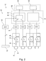
Figure 2 schematically shows internal components of an electrical test and measurement device according to the invention, -
Figure 3 schematically shows internal components of a measurement extension device according to the invention, -
Figure 4 shows a single analog channel of the measurement extension device ofFigure 3 in more detail, -
Figure 5 shows a detail ofFigure 4 , and -
Figure 6 shows a time chart of two different signals for determining a time delay of the measurement extension device. - In
Figure 1 , a test andmeasurement system 10 is shown that comprises an electrical test andmeasurement device 12 that is established by anoscilloscope 14 as well as ameasurement extension device 16 that is connected to the test andmeasurement device 12. - In the shown embodiment, the test and
measurement device 12 has fouranalog channels 18 that each comprises ananalog input 20, for instance a BNC input. Theanalog inputs 20 are positioned such that they can be connected easily, for instance at an outer surface of the test andmeasurement device 12. - Further, the test and
measurement device 12 comprises adigitizer input 22 that is connected to the separately formedmeasurement extension device 16. The connection is established by acable 24, for instance a flat conductor. In general, thecable 24 used ensures transmission of high bandwidth signals. - Moreover, the test and
measurement device 12 has adisplay 26 that is configured to illustrate signals received via theanalog channels 18. Further, thedisplay 26 is configured to display signals received via thedigitizer input 22. - As shown in
Figure 1 , themeasurement extension device 16 has fouranalog channels 28 that each comprises ananalog input 30. - Further, the
measurement extension device 16 has ananalog output interface 32 that is connected to thecable 24 such that the connection between the test andmeasurement device 12 and themeasurement extension device 16 is established via thecable 24 that connects thedigitizer input 22 and theanalog output interface 32. Due to theanalog output interface 32, analog signals are transmitted via thecable 24 towards the test andmeasurement device 12. - As shown in
Figure 1 , the test andmeasurement device 12 may comprise ahousing 34 wherein themeasurement extension device 16 comprises anouter box 36 for encompassing the internal components shown inFigure 3 as will be described later. - In
Figure 2 , the test andmeasurement device 12 is shown in more detail as internal components are illustrated, in particular afunctional unit 38. - In the shown embodiment, each
analog channel 18 of the electrical test andmeasurement device 12 comprises anattenuator circuit 40, anamplifier unit 42 and adigitizer 44 besides theanalog input 20. As shown, theamplifier unit 42 comprises avariable gain amplifier 46 that is used for signals having a high dynamic and high input bandwidth. - The
analog channels 18 are each allocated to asignal processing unit 48 that comprisesdifferent processing portions 50. In the shown embodiment, twodifferent processing portions 50 are provided wherein each processingportion 50 is allocated to twodifferent analog channels 18. - The
signal processing unit 48 is further connected to amemory 52, in particular a random access memory, that may also comprisedifferent memory portions 54 as shown inFigure 2 . - Despite the
analog channels 18 having thereown digitizers 44, anotherdigitizer 56 is provided that is allocated to thedigitizer input 22 configured to receive analog signals. Thus, the signals received via thedigitizer input 22 are digitized by thedigitizer 56 that is also connected to thesignal processing unit 48, in particular a signalprocessing unit portion 50. - In the input channel allocated to the
digitizer input 22, the analog signals received are directly forwarded to thedigitizer 56. Thus, no amplifying and/or attenuation of the signals input via thedigitizer input 22 take place within the test andmeasurement device 12. - The
signal processing unit 48, in particular the signalprocessing unit portion 50 connected to thedigitizer input 22, comprises adecimator 58 that is used to adapt the sample rate such that the predetermined maximum separate processing power of thesignal processing unit 48 is not exceeded. - For instance, the predetermined maximum sample rate processing power is 20 GS/s wherein the
decimator 58 decimates the sample rate of theseveral analog channels 18 as well as thedigitizer input 22 such that 8x 2.5 GS/s are provided for the fourinternal analog channels 18 as well as the fourexternal analog channels 28 established by themeasurement extension device 16. - Hence, the overall maximum sample rate processing power being available is split in a homogenous manner for all active
analog channels - In an alternative embodiment, the
decimator 58 is allocated to acertain processing portion 50 without affecting the other processing portion(s) 50 such that only the maximum sample rate processing power of theprocessing portion 50 is decimated appropriately. - In
Figure 3 , themeasurement extension device 16 is shown in more detail, in particular its internal components. - Each
analog channel 28 of themeasurement extension device 16 comprises anattenuator circuit 59 that is connected to thecorresponding analog input 30 and anamplifier unit 60 that comprises avariable gain amplifier 62. - The
amplifier unit 60 is connected with an isolatingunit 64 that is shown inFigure 4 in more detail. - Generally, the
different analog channels 28 are each connected with the commonanalog output interface 32 as shown inFigure 3 . - In
Figure 4 , asingle analog channel 28 is shown in more detail wherein theisolation unit 64 is also illustrated in more detail. - The
isolation unit 64 comprises an isolatedcontrol signal interface 66 that is configured to control theamplifier unit 60. The isolatorcontrol signal interface 66 may be provided by an optical isolation such that a galvanic isolation is established. - Further, the
isolation unit 64 comprises apower supply interface 68 that is also isolated with respect to the other signal lines as shown inFigure 4 . Thepower supply interface 68 is used to power theamplifier unit 60 appropriately. - Accordingly, the
measurement extension device 16 is controlled by the test andmeasurement device 12, in particular via the isolatedcontrol signal interface 66 wherein theamplifier unit 60 of themeasurement extension device 16 is also powered by the test andmeasurement device 12 when themeasurement extension device 16 is connected to thedigitizer input 22. - In
Figure 5 , another detail of asingle analog channel 28 is shown. Each analog channel may comprise a timedelay compensation unit 70 that is configured to compensate time delays introduced by theanalog channel 28, in particular its components such as theamplifier unit 60. - As shown in
Figure 5 , the timedelay compensation unit 70 comprises aswitch unit 72 that is connected to acalibration signal interface 74 as well as aninput channel 76 that is provided between theanalog input 30 and theamplifier unit 60. Particularly, the timedelay compensation unit 70 may be established as a part of theamplifier unit 60. - Hence, it is ensured that the time
delay compensation unit 70 is allocated to theanalog input 30 which is fed by a signal to be processed appropriately. - As shown in
Figure 6 , the timedelay compensation unit 70 may generate a calibration signal wherein a calibration signal sent to theamplifier unit 60, in particular thevariable gain amplifier 62, is compared with a signal received from theamplifier unit 60 in order to determine the occurring time delay T. Thus, the time delay T of theamplifier unit 60, in particular thevariable gain amplifier 62, can be determined appropriately and thus compensated. - The
several analog inputs 30 of themeasurement extension device 16 may be established by BNC inputs - In general, a possibility is provided that enables measurements requiring a high number of analog inputs. The
measurement extension device 16 is connected to the test andmeasurement device 12 in order to increase the number of analog channels of the test andmeasurement system 10. This means that the separately formedmeasurement extension device 16 can be used to extend or increase the capacity of the test andmeasurement device 12 for performing analog measurements in an appropriate manner. Accordingly, the user does not have to purchase a test andmeasurement device 12 having a high number of analog channels that are used rarely.
Claims (15)
- An electrical test and measurement device (12) with at least one analog channel (18) that comprises an analog input (20), an attenuator circuit (40), an amplifier unit (42), and a digitizer (46), wherein the electrical test and measurement device (12) comprises another digitizer (56) allocated to a digitizer input (22) of the electrical test and measurement device (12), wherein the digitizer input (22) is configured to be connected to a measurement extension device (16).
- The electrical test and measurement device (12) according to claim 1, wherein at least two analog channels (18) are provided, in particular four analog channels (18).
- The electrical test and measurement device (12) according to claim 1 or 2, wherein a signal processing unit (48) is provided.
- The electrical test and measurement device (12) according to claim 3, wherein the signal processing unit (48) has a predetermined maximum sample rate processing power.
- The electrical test and measurement device (12) according to claim 3 or 4, wherein the signal processing unit (48) comprises at least one decimator (58) configured to decimate the sample rate.
- The electrical test and measurement device (12) according to any of the preceding claims, wherein the electrical test and measurement device (12) is an oscilloscope (14).
- A measurement extension device (16) for being connected to an electrical test and measurement device (12), wherein the measurement extension device (16) has at least one analog channel (28) comprising an analog input (30), an attenuator circuit (59) and an amplifier unit (60), wherein the measurement extension device (16) has an analog output interface (32).
- The measurement extension device (16) according to claim 7, wherein the analog channel (28) further comprises an isolating unit (64) configured to isolate the analog output interface (32) from at least one of the attenuator circuit (40) and the amplifier unit (60).
- The measurement extension device (16) according to claim 8, wherein the isolating unit (64) comprises an isolated control signal interface (66) configured to control the amplifier unit (60).
- The measurement extension device (16) according to claim 8 or 9, wherein the isolating unit (64) comprises a power supply interface (68).
- The measurement extension device (16) according to any of the claims 7 to 10, wherein a time delay compensation unit (70) is provided that is configured to compensate time delays introduced by the analog channel (28), in particular wherein the time delay compensation unit (70) comprises a switch unit (72) allocated to the analog input (30) wherein the switch unit (70) is configured to switch between a calibration signal interface (74) and an input channel (76) allocated to the analog input (30).
- The measurement extension device (16) according to any of the claims 7 to 11, wherein the analog output interface (32) is configured to be connected with a test and measurement device (12).
- The measurement extension device (16) according to any of the claims 7 to 12, wherein the amplifier unit (60) comprises a variable gain amplifier (62).
- The measurement extension device (16) according to any of the claims 7 to 13, wherein at least two analog channels (28) are provided, in particular four analog channels (28).
- A test and measurement system (10) comprising a test and measurement device (12) according to any of the claims 1 to 6 and a measurement extension device (16) according to any of the claims 7 to 14.
Priority Applications (3)
| Application Number | Priority Date | Filing Date | Title |
|---|---|---|---|
| EP17171742.4A EP3404427B1 (en) | 2017-05-18 | 2017-05-18 | Electrical test and measurement device, measurement extension device as well as test and measurement system |
| US15/981,531 US11249115B2 (en) | 2017-05-18 | 2018-05-16 | Electrical test and measurement device, measurement extension device as well as test and measurement system |
| CN201810473348.0A CN108957083A (en) | 2017-05-18 | 2018-05-17 | Electrical test and measuring device, measurement expansion equipment and test and measuring system |
Applications Claiming Priority (1)
| Application Number | Priority Date | Filing Date | Title |
|---|---|---|---|
| EP17171742.4A EP3404427B1 (en) | 2017-05-18 | 2017-05-18 | Electrical test and measurement device, measurement extension device as well as test and measurement system |
Publications (2)
| Publication Number | Publication Date |
|---|---|
| EP3404427A1 true EP3404427A1 (en) | 2018-11-21 |
| EP3404427B1 EP3404427B1 (en) | 2024-11-13 |
Family
ID=58715122
Family Applications (1)
| Application Number | Title | Priority Date | Filing Date |
|---|---|---|---|
| EP17171742.4A Active EP3404427B1 (en) | 2017-05-18 | 2017-05-18 | Electrical test and measurement device, measurement extension device as well as test and measurement system |
Country Status (3)
| Country | Link |
|---|---|
| US (1) | US11249115B2 (en) |
| EP (1) | EP3404427B1 (en) |
| CN (1) | CN108957083A (en) |
Cited By (1)
| Publication number | Priority date | Publication date | Assignee | Title |
|---|---|---|---|---|
| US11293982B2 (en) | 2019-03-07 | 2022-04-05 | Rohde & Schwarz Gmbh & Co. Kg | Test method and test system |
Families Citing this family (1)
| Publication number | Priority date | Publication date | Assignee | Title |
|---|---|---|---|---|
| US12287368B2 (en) | 2022-05-25 | 2025-04-29 | Rohde & Schwarz Gmbh & Co. Kg | Method for generating a signal test specification, data processing circuit, and cloud system |
Citations (8)
| Publication number | Priority date | Publication date | Assignee | Title |
|---|---|---|---|---|
| US4743844A (en) * | 1986-12-19 | 1988-05-10 | Tektronix, Inc. | Self-adjusting oscilloscope |
| US4758963A (en) * | 1982-09-14 | 1988-07-19 | Analogic Corporation | Modular computing oscilloscope with high speed signal memory |
| US20080036726A1 (en) * | 2006-08-09 | 2008-02-14 | Rohde & Schwarz Gmbh & Co. Kg | System and method for processing and representing a sampled signal |
| EP2302400A1 (en) * | 2009-09-17 | 2011-03-30 | Tektronix, Inc. | Mixed signal acquisition system for a measurement instrument |
| US20130207641A1 (en) * | 2012-02-15 | 2013-08-15 | Agilent Technologies, Inc. | Digital oscilloscope comprising multiple data acquisition pathways |
| US20150054492A1 (en) * | 2013-08-22 | 2015-02-26 | Tektronix, Inc. | Isolated probe with digital multimeter or digital voltmeter |
| US20160139178A1 (en) * | 2013-04-24 | 2016-05-19 | Keysight Technologies, Inc. | Dual output high voltage active probe with output clamping and associated methods |
| US20170067940A1 (en) * | 2015-09-04 | 2017-03-09 | Ford Global Technologies, Llc | Isolated differential voltage probe for emi noise source |
Family Cites Families (6)
| Publication number | Priority date | Publication date | Assignee | Title |
|---|---|---|---|---|
| US4317199A (en) * | 1980-01-31 | 1982-02-23 | Tektronix, Inc. | Diagnostic extender test apparatus |
| US6320577B1 (en) * | 1998-11-03 | 2001-11-20 | Agilent Technologies, Inc. | System and method for graphically annotating a waveform display in a signal-measurement system |
| US7957938B2 (en) * | 2002-10-24 | 2011-06-07 | Lecroy Corporation | Method and apparatus for a high bandwidth oscilloscope utilizing multiple channel digital bandwidth interleaving |
| CN200958995Y (en) * | 2006-07-20 | 2007-10-10 | 朱明� | Microelement analyzer |
| CN105116263A (en) * | 2015-09-18 | 2015-12-02 | 成都比善科技开发有限公司 | Intelligent power monitoring device |
| CN106656178A (en) * | 2016-12-29 | 2017-05-10 | 郑州云海信息技术有限公司 | Signal processing device, system and method |
-
2017
- 2017-05-18 EP EP17171742.4A patent/EP3404427B1/en active Active
-
2018
- 2018-05-16 US US15/981,531 patent/US11249115B2/en active Active
- 2018-05-17 CN CN201810473348.0A patent/CN108957083A/en active Pending
Patent Citations (8)
| Publication number | Priority date | Publication date | Assignee | Title |
|---|---|---|---|---|
| US4758963A (en) * | 1982-09-14 | 1988-07-19 | Analogic Corporation | Modular computing oscilloscope with high speed signal memory |
| US4743844A (en) * | 1986-12-19 | 1988-05-10 | Tektronix, Inc. | Self-adjusting oscilloscope |
| US20080036726A1 (en) * | 2006-08-09 | 2008-02-14 | Rohde & Schwarz Gmbh & Co. Kg | System and method for processing and representing a sampled signal |
| EP2302400A1 (en) * | 2009-09-17 | 2011-03-30 | Tektronix, Inc. | Mixed signal acquisition system for a measurement instrument |
| US20130207641A1 (en) * | 2012-02-15 | 2013-08-15 | Agilent Technologies, Inc. | Digital oscilloscope comprising multiple data acquisition pathways |
| US20160139178A1 (en) * | 2013-04-24 | 2016-05-19 | Keysight Technologies, Inc. | Dual output high voltage active probe with output clamping and associated methods |
| US20150054492A1 (en) * | 2013-08-22 | 2015-02-26 | Tektronix, Inc. | Isolated probe with digital multimeter or digital voltmeter |
| US20170067940A1 (en) * | 2015-09-04 | 2017-03-09 | Ford Global Technologies, Llc | Isolated differential voltage probe for emi noise source |
Cited By (1)
| Publication number | Priority date | Publication date | Assignee | Title |
|---|---|---|---|---|
| US11293982B2 (en) | 2019-03-07 | 2022-04-05 | Rohde & Schwarz Gmbh & Co. Kg | Test method and test system |
Also Published As
| Publication number | Publication date |
|---|---|
| US11249115B2 (en) | 2022-02-15 |
| EP3404427B1 (en) | 2024-11-13 |
| US20180335453A1 (en) | 2018-11-22 |
| CN108957083A (en) | 2018-12-07 |
Similar Documents
| Publication | Publication Date | Title |
|---|---|---|
| EP3273256B1 (en) | Multi-band noise reduction systems and methods | |
| KR100421277B1 (en) | Architecture for rf signal automatic test equipment | |
| EP2853902B1 (en) | Switched load time-domain reflectometer de-embed probe | |
| EP2853912A1 (en) | Time-domain reflectometer de-embed probe | |
| US10317503B2 (en) | Testing device comprising circuitry to calculate a correction value for calibrating channel loss | |
| CN104729539B (en) | Measurement system comprising an accessory with an internal calibration signal | |
| EP3540447A1 (en) | Test and measurement management | |
| JP6622970B2 (en) | Test measurement system and accessory compensation method | |
| US20220334144A1 (en) | Multi-mode measurement probe | |
| US20230266369A1 (en) | Systems, devices, and methods for measuring direct current/low frequency signal components | |
| US11249115B2 (en) | Electrical test and measurement device, measurement extension device as well as test and measurement system | |
| EP2330415B1 (en) | Sequentially fired high dynamic range NDT/NDI inspection device | |
| JPS6030898B2 (en) | Logic analyzer input device | |
| US20190094327A1 (en) | Calibration apparatus, calibration system and method for calibrating at least one of the signal generator and a signal analyzer | |
| JP2004028983A (en) | Measuring equipment and measuring method | |
| US7634370B2 (en) | Waveform input circuit, waveform observation unit and semiconductor test apparatus | |
| KR101894833B1 (en) | Performance Testing System for Frequency Synthesis Apparatus | |
| JP2007316054A (en) | Signal path calibration method for signal analysis system | |
| US11054467B2 (en) | Dynamic probe, dynamic measurement system and method for probing a dynamic data signal | |
| KR20210111201A (en) | Quality measuring device, measuring method thereof and recording medium thereof | |
| US7282935B2 (en) | Regenerator probe | |
| US20260003020A1 (en) | Test fixture, calibration setup and method of calibrating a test and/or measurement instrument | |
| US11125779B2 (en) | Probe with radio frequency power detector, test system and test method | |
| US12115020B2 (en) | Two-dimensional array ultrasonic probe and addition circuit | |
| JP5239395B2 (en) | Waveform measuring device |
Legal Events
| Date | Code | Title | Description |
|---|---|---|---|
| PUAI | Public reference made under article 153(3) epc to a published international application that has entered the european phase |
Free format text: ORIGINAL CODE: 0009012 |
|
| STAA | Information on the status of an ep patent application or granted ep patent |
Free format text: STATUS: THE APPLICATION HAS BEEN PUBLISHED |
|
| AK | Designated contracting states |
Kind code of ref document: A1 Designated state(s): AL AT BE BG CH CY CZ DE DK EE ES FI FR GB GR HR HU IE IS IT LI LT LU LV MC MK MT NL NO PL PT RO RS SE SI SK SM TR |
|
| AX | Request for extension of the european patent |
Extension state: BA ME |
|
| STAA | Information on the status of an ep patent application or granted ep patent |
Free format text: STATUS: REQUEST FOR EXAMINATION WAS MADE |
|
| 17P | Request for examination filed |
Effective date: 20181206 |
|
| RBV | Designated contracting states (corrected) |
Designated state(s): AL AT BE BG CH CY CZ DE DK EE ES FI FR GB GR HR HU IE IS IT LI LT LU LV MC MK MT NL NO PL PT RO RS SE SI SK SM TR |
|
| STAA | Information on the status of an ep patent application or granted ep patent |
Free format text: STATUS: EXAMINATION IS IN PROGRESS |
|
| 17Q | First examination report despatched |
Effective date: 20211130 |
|
| RIC1 | Information provided on ipc code assigned before grant |
Ipc: G01R 19/25 20060101ALI20211123BHEP Ipc: G01R 13/00 20060101AFI20211123BHEP |
|
| GRAP | Despatch of communication of intention to grant a patent |
Free format text: ORIGINAL CODE: EPIDOSNIGR1 |
|
| STAA | Information on the status of an ep patent application or granted ep patent |
Free format text: STATUS: GRANT OF PATENT IS INTENDED |
|
| INTG | Intention to grant announced |
Effective date: 20240812 |
|
| GRAS | Grant fee paid |
Free format text: ORIGINAL CODE: EPIDOSNIGR3 |
|
| GRAA | (expected) grant |
Free format text: ORIGINAL CODE: 0009210 |
|
| STAA | Information on the status of an ep patent application or granted ep patent |
Free format text: STATUS: THE PATENT HAS BEEN GRANTED |
|
| AK | Designated contracting states |
Kind code of ref document: B1 Designated state(s): AL AT BE BG CY CZ DE DK EE ES FI FR GB GR HR HU IS IT LT LU LV MC MK MT NL NO PL PT RO RS SE SI SK SM TR |
|
| P01 | Opt-out of the competence of the unified patent court (upc) registered |
Free format text: CASE NUMBER: UPC_APP_414910/2023 Effective date: 20230525 |
|
| RBV | Designated contracting states (corrected) |
Designated state(s): AL AT BE BG CY CZ DE DK EE ES FI FR GB GR HR HU IS IT LT LU LV MC MK MT NL NO PL PT RO RS SE SI SK SM TR |
|
| REG | Reference to a national code |
Ref country code: GB Ref legal event code: FG4D |
|
| REG | Reference to a national code |
Ref country code: DE Ref legal event code: R096 Ref document number: 602017086065 Country of ref document: DE |
|
| REG | Reference to a national code |
Ref country code: LT Ref legal event code: MG9D |
|
| REG | Reference to a national code |
Ref country code: NL Ref legal event code: MP Effective date: 20241113 |
|
| PG25 | Lapsed in a contracting state [announced via postgrant information from national office to epo] |
Ref country code: HR Free format text: LAPSE BECAUSE OF FAILURE TO SUBMIT A TRANSLATION OF THE DESCRIPTION OR TO PAY THE FEE WITHIN THE PRESCRIBED TIME-LIMIT Effective date: 20241113 Ref country code: PT Free format text: LAPSE BECAUSE OF FAILURE TO SUBMIT A TRANSLATION OF THE DESCRIPTION OR TO PAY THE FEE WITHIN THE PRESCRIBED TIME-LIMIT Effective date: 20250313 Ref country code: IS Free format text: LAPSE BECAUSE OF FAILURE TO SUBMIT A TRANSLATION OF THE DESCRIPTION OR TO PAY THE FEE WITHIN THE PRESCRIBED TIME-LIMIT Effective date: 20250313 |
|
| PG25 | Lapsed in a contracting state [announced via postgrant information from national office to epo] |
Ref country code: FI Free format text: LAPSE BECAUSE OF FAILURE TO SUBMIT A TRANSLATION OF THE DESCRIPTION OR TO PAY THE FEE WITHIN THE PRESCRIBED TIME-LIMIT Effective date: 20241113 Ref country code: NL Free format text: LAPSE BECAUSE OF FAILURE TO SUBMIT A TRANSLATION OF THE DESCRIPTION OR TO PAY THE FEE WITHIN THE PRESCRIBED TIME-LIMIT Effective date: 20241113 |
|
| REG | Reference to a national code |
Ref country code: AT Ref legal event code: MK05 Ref document number: 1742069 Country of ref document: AT Kind code of ref document: T Effective date: 20241113 |
|
| PG25 | Lapsed in a contracting state [announced via postgrant information from national office to epo] |
Ref country code: BG Free format text: LAPSE BECAUSE OF FAILURE TO SUBMIT A TRANSLATION OF THE DESCRIPTION OR TO PAY THE FEE WITHIN THE PRESCRIBED TIME-LIMIT Effective date: 20241113 |
|
| PG25 | Lapsed in a contracting state [announced via postgrant information from national office to epo] |
Ref country code: ES Free format text: LAPSE BECAUSE OF FAILURE TO SUBMIT A TRANSLATION OF THE DESCRIPTION OR TO PAY THE FEE WITHIN THE PRESCRIBED TIME-LIMIT Effective date: 20241113 |
|
| PG25 | Lapsed in a contracting state [announced via postgrant information from national office to epo] |
Ref country code: NO Free format text: LAPSE BECAUSE OF FAILURE TO SUBMIT A TRANSLATION OF THE DESCRIPTION OR TO PAY THE FEE WITHIN THE PRESCRIBED TIME-LIMIT Effective date: 20250213 |
|
| PG25 | Lapsed in a contracting state [announced via postgrant information from national office to epo] |
Ref country code: LV Free format text: LAPSE BECAUSE OF FAILURE TO SUBMIT A TRANSLATION OF THE DESCRIPTION OR TO PAY THE FEE WITHIN THE PRESCRIBED TIME-LIMIT Effective date: 20241113 Ref country code: GR Free format text: LAPSE BECAUSE OF FAILURE TO SUBMIT A TRANSLATION OF THE DESCRIPTION OR TO PAY THE FEE WITHIN THE PRESCRIBED TIME-LIMIT Effective date: 20250214 Ref country code: AT Free format text: LAPSE BECAUSE OF FAILURE TO SUBMIT A TRANSLATION OF THE DESCRIPTION OR TO PAY THE FEE WITHIN THE PRESCRIBED TIME-LIMIT Effective date: 20241113 |
|
| PG25 | Lapsed in a contracting state [announced via postgrant information from national office to epo] |
Ref country code: PL Free format text: LAPSE BECAUSE OF FAILURE TO SUBMIT A TRANSLATION OF THE DESCRIPTION OR TO PAY THE FEE WITHIN THE PRESCRIBED TIME-LIMIT Effective date: 20241113 |
|
| PG25 | Lapsed in a contracting state [announced via postgrant information from national office to epo] |
Ref country code: RS Free format text: LAPSE BECAUSE OF FAILURE TO SUBMIT A TRANSLATION OF THE DESCRIPTION OR TO PAY THE FEE WITHIN THE PRESCRIBED TIME-LIMIT Effective date: 20250213 |
|
| PG25 | Lapsed in a contracting state [announced via postgrant information from national office to epo] |
Ref country code: SM Free format text: LAPSE BECAUSE OF FAILURE TO SUBMIT A TRANSLATION OF THE DESCRIPTION OR TO PAY THE FEE WITHIN THE PRESCRIBED TIME-LIMIT Effective date: 20241113 |
|
| PG25 | Lapsed in a contracting state [announced via postgrant information from national office to epo] |
Ref country code: DK Free format text: LAPSE BECAUSE OF FAILURE TO SUBMIT A TRANSLATION OF THE DESCRIPTION OR TO PAY THE FEE WITHIN THE PRESCRIBED TIME-LIMIT Effective date: 20241113 |
|
| PG25 | Lapsed in a contracting state [announced via postgrant information from national office to epo] |
Ref country code: EE Free format text: LAPSE BECAUSE OF FAILURE TO SUBMIT A TRANSLATION OF THE DESCRIPTION OR TO PAY THE FEE WITHIN THE PRESCRIBED TIME-LIMIT Effective date: 20241113 |
|
| PG25 | Lapsed in a contracting state [announced via postgrant information from national office to epo] |
Ref country code: RO Free format text: LAPSE BECAUSE OF FAILURE TO SUBMIT A TRANSLATION OF THE DESCRIPTION OR TO PAY THE FEE WITHIN THE PRESCRIBED TIME-LIMIT Effective date: 20241113 |
|
| PG25 | Lapsed in a contracting state [announced via postgrant information from national office to epo] |
Ref country code: SK Free format text: LAPSE BECAUSE OF FAILURE TO SUBMIT A TRANSLATION OF THE DESCRIPTION OR TO PAY THE FEE WITHIN THE PRESCRIBED TIME-LIMIT Effective date: 20241113 |
|
| PG25 | Lapsed in a contracting state [announced via postgrant information from national office to epo] |
Ref country code: CZ Free format text: LAPSE BECAUSE OF FAILURE TO SUBMIT A TRANSLATION OF THE DESCRIPTION OR TO PAY THE FEE WITHIN THE PRESCRIBED TIME-LIMIT Effective date: 20241113 |
|
| PG25 | Lapsed in a contracting state [announced via postgrant information from national office to epo] |
Ref country code: IT Free format text: LAPSE BECAUSE OF FAILURE TO SUBMIT A TRANSLATION OF THE DESCRIPTION OR TO PAY THE FEE WITHIN THE PRESCRIBED TIME-LIMIT Effective date: 20241113 |
|
| REG | Reference to a national code |
Ref country code: DE Ref legal event code: R097 Ref document number: 602017086065 Country of ref document: DE |
|
| PG25 | Lapsed in a contracting state [announced via postgrant information from national office to epo] |
Ref country code: SE Free format text: LAPSE BECAUSE OF FAILURE TO SUBMIT A TRANSLATION OF THE DESCRIPTION OR TO PAY THE FEE WITHIN THE PRESCRIBED TIME-LIMIT Effective date: 20241113 |
|
| PLBE | No opposition filed within time limit |
Free format text: ORIGINAL CODE: 0009261 |
|
| STAA | Information on the status of an ep patent application or granted ep patent |
Free format text: STATUS: NO OPPOSITION FILED WITHIN TIME LIMIT |
|
| 26N | No opposition filed |
Effective date: 20250814 |
|
| PG25 | Lapsed in a contracting state [announced via postgrant information from national office to epo] |
Ref country code: LU Free format text: LAPSE BECAUSE OF NON-PAYMENT OF DUE FEES Effective date: 20250518 |
|
| REG | Reference to a national code |
Ref country code: BE Ref legal event code: MM Effective date: 20250531 |
|
| PG25 | Lapsed in a contracting state [announced via postgrant information from national office to epo] |
Ref country code: MC Free format text: LAPSE BECAUSE OF FAILURE TO SUBMIT A TRANSLATION OF THE DESCRIPTION OR TO PAY THE FEE WITHIN THE PRESCRIBED TIME-LIMIT Effective date: 20241113 |
|
| PGFP | Annual fee paid to national office [announced via postgrant information from national office to epo] |
Ref country code: GB Payment date: 20260324 Year of fee payment: 10 |
|
| PG25 | Lapsed in a contracting state [announced via postgrant information from national office to epo] |
Ref country code: BE Free format text: LAPSE BECAUSE OF NON-PAYMENT OF DUE FEES Effective date: 20250531 |
|
| PG25 | Lapsed in a contracting state [announced via postgrant information from national office to epo] |
Ref country code: LT Free format text: LAPSE BECAUSE OF FAILURE TO SUBMIT A TRANSLATION OF THE DESCRIPTION OR TO PAY THE FEE WITHIN THE PRESCRIBED TIME-LIMIT Effective date: 20241113 |
|
| PGFP | Annual fee paid to national office [announced via postgrant information from national office to epo] |
Ref country code: DE Payment date: 20260520 Year of fee payment: 10 |
|
| PGFP | Annual fee paid to national office [announced via postgrant information from national office to epo] |
Ref country code: FR Payment date: 20260522 Year of fee payment: 10 |
|
| PG25 | Lapsed in a contracting state [announced via postgrant information from national office to epo] |
Ref country code: CY Free format text: LAPSE BECAUSE OF FAILURE TO SUBMIT A TRANSLATION OF THE DESCRIPTION OR TO PAY THE FEE WITHIN THE PRESCRIBED TIME-LIMIT Effective date: 20241113 |