EP3403121B1 - Fotonische plattform mit lichtübertragenden zwischenschichtübergängen - Google Patents
Fotonische plattform mit lichtübertragenden zwischenschichtübergängen Download PDFInfo
- Publication number
- EP3403121B1 EP3403121B1 EP17740930.7A EP17740930A EP3403121B1 EP 3403121 B1 EP3403121 B1 EP 3403121B1 EP 17740930 A EP17740930 A EP 17740930A EP 3403121 B1 EP3403121 B1 EP 3403121B1
- Authority
- EP
- European Patent Office
- Prior art keywords
- waveguide
- silicon
- layer
- silicon nitride
- platform
- Prior art date
- Legal status (The legal status is an assumption and is not a legal conclusion. Google has not performed a legal analysis and makes no representation as to the accuracy of the status listed.)
- Active
Links
Images


Classifications
-
- G—PHYSICS
- G02—OPTICS
- G02B—OPTICAL ELEMENTS, SYSTEMS OR APPARATUS
- G02B6/00—Light guides; Structural details of arrangements comprising light guides and other optical elements, e.g. couplings
- G02B6/10—Light guides; Structural details of arrangements comprising light guides and other optical elements, e.g. couplings of the optical waveguide type
- G02B6/12—Light guides; Structural details of arrangements comprising light guides and other optical elements, e.g. couplings of the optical waveguide type of the integrated circuit kind
- G02B6/122—Basic optical elements, e.g. light-guiding paths
-
- G—PHYSICS
- G02—OPTICS
- G02B—OPTICAL ELEMENTS, SYSTEMS OR APPARATUS
- G02B6/00—Light guides; Structural details of arrangements comprising light guides and other optical elements, e.g. couplings
- G02B6/10—Light guides; Structural details of arrangements comprising light guides and other optical elements, e.g. couplings of the optical waveguide type
- G02B6/12—Light guides; Structural details of arrangements comprising light guides and other optical elements, e.g. couplings of the optical waveguide type of the integrated circuit kind
- G02B6/12002—Three-dimensional structures
-
- G—PHYSICS
- G02—OPTICS
- G02B—OPTICAL ELEMENTS, SYSTEMS OR APPARATUS
- G02B6/00—Light guides; Structural details of arrangements comprising light guides and other optical elements, e.g. couplings
- G02B6/10—Light guides; Structural details of arrangements comprising light guides and other optical elements, e.g. couplings of the optical waveguide type
- G02B6/12—Light guides; Structural details of arrangements comprising light guides and other optical elements, e.g. couplings of the optical waveguide type of the integrated circuit kind
- G02B2006/12035—Materials
- G02B2006/12038—Glass (SiO2 based materials)
-
- G—PHYSICS
- G02—OPTICS
- G02B—OPTICAL ELEMENTS, SYSTEMS OR APPARATUS
- G02B6/00—Light guides; Structural details of arrangements comprising light guides and other optical elements, e.g. couplings
- G02B6/10—Light guides; Structural details of arrangements comprising light guides and other optical elements, e.g. couplings of the optical waveguide type
- G02B6/12—Light guides; Structural details of arrangements comprising light guides and other optical elements, e.g. couplings of the optical waveguide type of the integrated circuit kind
- G02B2006/12035—Materials
- G02B2006/12061—Silicon
-
- G—PHYSICS
- G02—OPTICS
- G02B—OPTICAL ELEMENTS, SYSTEMS OR APPARATUS
- G02B6/00—Light guides; Structural details of arrangements comprising light guides and other optical elements, e.g. couplings
- G02B6/10—Light guides; Structural details of arrangements comprising light guides and other optical elements, e.g. couplings of the optical waveguide type
- G02B6/12—Light guides; Structural details of arrangements comprising light guides and other optical elements, e.g. couplings of the optical waveguide type of the integrated circuit kind
- G02B6/122—Basic optical elements, e.g. light-guiding paths
- G02B6/1228—Tapered waveguides, e.g. integrated spot-size transformers
-
- G—PHYSICS
- G02—OPTICS
- G02B—OPTICAL ELEMENTS, SYSTEMS OR APPARATUS
- G02B6/00—Light guides; Structural details of arrangements comprising light guides and other optical elements, e.g. couplings
- G02B6/10—Light guides; Structural details of arrangements comprising light guides and other optical elements, e.g. couplings of the optical waveguide type
- G02B6/12—Light guides; Structural details of arrangements comprising light guides and other optical elements, e.g. couplings of the optical waveguide type of the integrated circuit kind
- G02B6/122—Basic optical elements, e.g. light-guiding paths
- G02B6/125—Bends, branchings or intersections
Definitions
- the present disclosure relates generally to silicon photonics and, more particularly, to silicon photonic platforms or material layer stacks.
- Silicon photonics is an emerging technology that enables fabrication of fast, low-cost and high-density photonic devices for a variety of uses and applications, notably in relation to optical network switching.
- Photonic switch fabrics which are capable of switching optical signals without conversion to the digital domain, are an area of particular interest.
- a silicon photonic switch typically incorporates a number of optical waveguides of varying lengths, multiple optical switch cells, and multiple waveguide crossings having intersecting waveguides.
- a silicon photonic device such as a silicon photonic switch
- SOI silicon-on-insulator
- a silicon photonic switch can be fabricated using a commercially available "silicon-on-insulator" (SOI) wafer composed of a thin layer of silicon (typically 150-350 nm thick) disposed on a layer of buried oxide (e.g. silicon dioxide) which is, in turn, supported on a silicon substrate typically several hundred micrometers thick.
- SOI silicon-on-insulator
- the fabrication of photonic devices requires a number of steps that include, for example, chemical vapor deposition and patterning of layers to form waveguides using lithography and etching. Huang, Y.
- CN 102944912 A describes a silicon-on-insulator (SOI)-based three-dimensional crossed waveguide wherein an adjacent two-layer waveguide structure constitutes an optical upward or downward coupling structure, and a top-layer waveguide is no longer disconnected.
- SOI silicon-on-insulator
- a silicon photonic switch fabric imposes demanding requirements in terms of optical performance (e.g. insertion loss, crosstalk) and optical component density.
- the insertion loss can be attributed primarily to a small number of sources: fiber-to-integrated-circuit coupling loss, waveguide scattering loss, switch cell insertion loss, and waveguide crossing loss.
- Waveguide crossings are necessary in switch fabrics. In large switch fabrics, there may be a significant number of waveguide crossings which cause losses and crosstalk.
- the waveguide scattering loss is relatively high, i.e. approximately 2 dB/cm for strongly confining strip waveguides. In a large switch matrix, therefore, long optical paths can cause a large scattering loss to accumulate, and many crossings can cause crosstalk to accumulate.
- the silicon photonic platform includes at least two silicon nitride light-guiding layers (optical transport layers or waveguides) disposed above an active silicon light-guiding layer, which are hereinafter referred to more succinctly as the "active silicon layer” and the "silicon nitride layers".
- Waveguides fabricated from silicon nitride (SiN) have been found to exhibit much lower propagation loss than silicon nanowire waveguides.
- the silicon nitride layer that is immediately above the active silicon layer is referred to as the first silicon nitride layer.
- the silicon nitride layer immediately above the first silicon nitride layer is referred to as the second silicon nitride layer.
- the first and second silicon nitride layers may be separated from the silicon layer and from themselves by buffer layers (i.e. spacers or separation layers) of silicon dioxide or another suitably low refractive index material.
- Interlayer transitions are implemented between two immediately consecutive layers using, for example, adiabatic tapers, in which the "source” waveguide is tapered down to a small tip, while in the same span the "target” waveguide is tapered up from a small tip to the desired waveguide width for that layer.
- Low-loss interlayer transitions route the propagating signal from the silicon layer to the first nitride layer and back to the silicon layer.
- the low-loss routing is implemented when the projected loss in the silicon layer exceeds the projected loss of two interlayer transitions and the projected loss of the silicon nitride waveguide over the target routing distance.
- Waveguide crossings are implemented using two interlayer transitions to connect the silicon waveguide layer to the second nitride layer, using the first silicon nitride layer as an intermediate layer, and routing the second silicon nitride layer waveguide above one or a series of waveguides in the silicon layer.
- the multi-layer waveguide crossing (which can be thought of as an "overpass") is advantageously implemented when the sum of the insertion losses of a series of single-layer crossings (which in the prior art would be implemented in the silicon layer) exceeds the projected loss from the four relevant interlayer transitions (i.e.
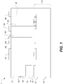
- a silicon photonic platform (or “stack” or “integrated photonic platform”) is denoted by reference numeral 2.
- the photonic platform 2 includes a silicon-on-insulator (SOI) wafer 10 composed of a silicon (Si) substrate 12 supporting a buried oxide layer 14 which may be formed of silica (SiO 2 ) or any equivalent insulating material. In other embodiments, the substrate supporting the buried oxide layer may be formed of another suitable material.
- the platform 2 includes an active silicon layer 16 deposited on the buried oxide layer 14.
- the active silicon layer 16 is an optical transport layer capable of conducting light. This silicon layer is said to be active as it actively transports light unlike the (passive) silicon substrate which does not transport light.
- the platform 2 includes two additional light-guiding layers (optical transport layers) made of silicon nitride (hereinafter denoted "SiN" although it will be appreciated that the SiN may be mainly of the form of Si x N y , including stoichiometric silicon nitride, Si 3 N 4 ).
- SiN silicon nitride
- the platform 2 includes a first silicon nitride layer 18 separated from the active silicon layer by a first spacer (or separation layer) 17.
- the first silicon nitride layer 18 and the active silicon layer 16 constitute a first light-transferring interlayer transition.
- the platform 2 also includes a second silicon nitride layer 20 that is optionally covered by a cladding 21.
- the second silicon nitride layer 20 is separated from the first silicon layer 18 by a second spacer (or separation layer) 19.
- the second silicon nitride layer 20 and the first silicon nitride layer 18 constitute a second light-transferring interlayer transition.
- the platform may also include a heater, e.g. a TiN metal heater 22 and a plurality of top contacts 24 and metal vias 26.
- the platform may also include one or more include germanium photodiodes and/or PN junctions for modulators.
- the buried oxide layer, the first spacer (first separation layer), the second spacer (second separation layer) and the cladding are all made of silica although it will be appreciated that other suitable materials may be utilized.
- the layers of the photonic platform (stack) 2 thus define optical waveguides at different layer depths (i.e. different heights or vertical levels) that are supported directly or indirectly by the silicon substrate.
- the layers of silicon nitride, silicon and silica may be deposited on the SOI wafer using various existing CMOS-compatible fabrication techniques, e.g. chemical vapor deposition (CVD), lithography and etching. Layers may be deposited onto the SOI wafer using front-end-of line (FEOL) processes to form a FEOL layer stack or back-end-of-line (BEOL) processes to form a BEOL layer stack.
- FEOL front-end-of line
- BEOL back-end-of-line
- first and second silicon nitride layers 18, 20 are thicker than the active silicon layer 16.
- the first and second silicon nitride layers 18, 20 in this embodiment are also thicker than the first and second spacers (separation layers) 17, 19.
- the first and second silicon nitride layers 18, 20 are twice as thick as the first and second spacers 17, 19. In one embodiment, the first and second silicon nitride layers 18, 20 are equally thick. In one embodiment, the first and second spacers 17, 19 are equally thick. In another embodiment, the second spacer (second separation layer) 19 is thicker than the first spacer (first separation layer) 17.
- each of the first and second silicon nitride layers has a thickness of 400 nm +/-20%
- the buried oxide layer has a thickness of 2-3 ⁇ m +/-20%
- each of the first and second spacers has a thickness of 200 nm +/-20%
- the active silicon layer has a thickness of 150 nm +/-20%.
- the active silicon layer may be a partially etched slab having sides portions that are thinner than a central portion. The side portions of the slab may have a thickness of 65 nm +/-20% while the central portion has a thickness of 150 nm +/-20%.
- each of the first and second silicon nitride layers also has a thickness of 400 nm +/-20%
- the buried oxide layer has a thickness of 2 ⁇ m +/-20%
- the first spacer has a thickness of 200 nm +/-20%
- the second spacer has a thickness of 360 nm +/-20%
- the active silicon layer has a thickness of 220 nm +/-20%.
- the active silicon layer may be a partially etched slab having sides portions that are thinner than a central portion. The side portions of the slab may have a thickness of 90 nm +/-20% while the central portion has a thickness of 220 nm +/-20%.
- the active silicon layer 16, the first silicon nitride layer 18 and the second silicon nitride layer 20 function as three levels of optical transport layers that cooperate to transmit light from the active silicon layer up to the second nitride layer and then back to the silicon layer.
- these optical transport layers act as steps, each disposed a different depth, that cause the light to ascend to a higher level or to descend to a lower level.
- This arrangement of step-like levels thus enables vertical transmission of light, thereby functioning to some extent like an optical via.
- This technology can be exploited to efficiently conduct light over one or more waveguides.
- the step-like layers can be used to construct a low-loss, low-crosstalk waveguide crossing, which is particularly useful in the context of fabricating low-loss, low-crosstalk photonic switch fabrics.
- Figure 2 depicts a waveguide crossing composed of a silicon waveguide 30 and a silicon nitride waveguide 32 passing over the silicon waveguide 30, thus defining a low-loss, low-crosstalk "overpass".
- the silicon waveguide 30 is orthogonal to the silicon nitride waveguide 32.
- An orthogonal crossing angle minimizes crosstalk; however, a non-orthogonal crossing angle, though suboptimal, may still be used in other embodiments.
- Waveguide crossings using only a single silicon nitride layer over the active silicon layer exhibit limited performance. The explanation can be summarized as follows. In order to couple light into the single silicon nitride layer, the silicon and silicon nitride layers must be close enough to interact.
- the double layer of silicon nitride enables light to be coupled while augmenting the gap between the silicon nitride and the silicon waveguide crossing underneath the span of silicon nitride.
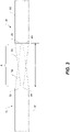
- Figure 3 depicts an interlayer transition between a first waveguide 50 and a second waveguide 60 that is slightly vertically offset from the first waveguide 50. This transition may be between the active silicon layer and the first silicon nitride layer or between the first and second silicon nitride layers.
- the first waveguide 50 is a lower waveguide and the second waveguide 60 is an upper waveguide.
- the first waveguide 50 has a first tapered end section 52 that at least partially overlies a corresponding second tapered end section 62 of the second waveguide 60 within an overlap region R.
- the first tapered end section 52 may be coupled to, or formed integrally with, a channel or strip waveguide section of the first waveguide 50 at a waveguide interface 53 between a first waveguide section 55 and the first tapered end section 52.
- the second tapered end section 62 of the second waveguide 60 may be coupled to, or formed integrally with, a corresponding channel or strip waveguide section at a waveguide interface 63 between the second tapered end section 62 and a second waveguide section 65.
- the tapered end sections 52, 62 may be substantially axially aligned in a linear direction defined by the waveguide sections and are disposed at different layer depths so as to be at least partially overlapping.
- the first tapered end section 52 narrows in width from a first width at the waveguide interface 53, which may in some cases be substantially equal to a width of waveguide section 55, to a second width at a first end facet 54 or "tip".
- the second tapered end section 62 also narrows from a first width at the waveguide interface 63 to a second width at the second end facet 64 or tip, but in an opposite direction to the first tapered end section.
- the tapered end sections 52, 62 have substantially equal lengths and are both laterally (e.g., side-to-side in the linear direction) and axially (e.g., end-to-end-in the linear direction) aligned.
- the end facet 64 of the second waveguide 60 may lie substantially above the waveguide interface 53 of the first waveguide and likewise the end facet 54 of the first waveguide 50 may lie substantially underneath the waveguide interface 63 of the second waveguide 60.
- the first end facet 54 may be slightly horizontally offset from the second waveguide interface 63 and the second end facet 64 may be slightly horizontally offset from the first waveguide interface 53.
- tapered end sections 52, 62 may in other cases not have substantially equal lengths or be aligned, either laterally or axially, or both, within the overlap region. Different sizes ratios and/or spatial orientations of the tapered end sections may be implemented depending on the particular use or application of the photonic platform.
- the interlayer transitions between the first (lower) waveguide 50 and the second (upper) waveguide 60 may have adiabatic tapers.
- An adiabatic taper enables an adiabatic mode transformation across the interlayer transition.
- An adiabatic mode transformation transfers the propagating optical energy from one mode to another, which is induced by the changing geometry of the waveguide in which the optical energy is confined, but does not affect the mode order, e.g. a TMo to TE 1 transformation, a TE 1 to TE 0 transformation, etc.
- the adiabatic tapers taper linearly toward each other to form a symmetrical and laterally aligned geometry for the interlayer transition.
- a taper length L of 100-150 ⁇ m has been found to provide a low-loss interlayer transition.
- the optical loss of the interlayer transition is also affected by the size of the waveguide tips (end facets). It is desirable to make the tips as small as possible.
- the tapered end sections 52, 62 are spaced apart vertically by a relatively small distance as defined by a layer thickness of the separation layer (or spacer layer) formed between the tapered end sections 52, 62.
- the separation layer may be formed in the photonic platform with a thickness of approximately 50 nanometers or some other thickness within a range of thicknesses that includes 50 nanometers, such as between about 20 and 80 nanometers. Due to their relatively close vertical proximity, on account of the small thickness of the separation layer, the first and second tapered end sections constitute a composite waveguide (interlayer transition) that transfers light in either direction between the first and second waveguides.
- an optical mode propagating (e.g., from left-to-right) in the first waveguide section 50 is coupled into the tapered end section 52, which gradually narrows in width as the second tapered end section gradually widens.
- Gradual tapering allows the propagating optical mode to transform in the direction of propagation within the overlap region R from a mode that may be carried in the first waveguide to a mode that may be carried in the second waveguide.
- optical modes initially being conducted by the first waveguide may be transferred or redistributed into the second waveguide and vice versa.
- the photonic platform thus behaves bidirectionally.
- the first and second tapered end sections 52, 62 may be shaped so that each respective width transition is adiabatic in nature.
- the first tapered end section may have a width of between about 700 and 1500 nanometers at the waveguide interface, tapering down to a width not exceeding about 300 nanometers at the end facet, in some cases, between about 140 and 180 nanometers, while in other cases, depending on the lithographic and fabrication resolution of the process or processes used to fabricate the photonic platform, less than 140 nanometers.
- the first tapered end section may also have a length of between about 5 and 500 micrometers, or in some cases between about 5 and 100 micrometers.
- the second tapered end section 62 may have a shape configuration that encourages adiabatic transformation of optical modes.
- the second tapered end section may have a width of between about 400 and 700 nanometers at waveguide interface, which narrows down to a width not exceeding about 250 nanometers at the end facet, in some cases, between about 140 and 180 nanometers, while in other cases, as permitted by lithographic and fabrication resolution, less than 140 nanometers.
- the second tapered end section 62 may also have a length of between about 5 and 500 micrometers, or in some cases between about 100 and 150 micrometers. In some cases, the first and second tapered end sections 52, 62 may have substantially the same length.
- the first and second waveguides 50, 60 may have different layer thicknesses.
- the first tapered end section, first waveguide section, and end facet may each have a layer thickness of approximately 400 nanometers or some other thickness within a range that includes 400 nanometers, such as between about 300 and 500 nanometers.
- the second tapered end section, second waveguide section, and second end facet may each have a layer thickness of approximately 150 nanometers or some other thickness within a range that includes 150 nanometers, such as between about 100 and 200 nanometers.
- other dimensions not within the example ranges specifically described may be possible as well depending on the particular use or application of the photonic platform.
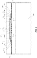
- Figure 4 depicts a photonic platform having low-loss, low-crosstalk waveguide crossing formed by disposing a second silicon nitride layer over silicon waveguides.
- the platform is composed of a stack of layers, namely a silicon substrate 70 onto which a buried oxide layer 72 is deposited.
- An active silicon layer 74 is deposited on the buried oxide layer.
- One or more silicon waveguides 75 are formed on the buried oxide layer at the same depth as the active silicon layer.
- the silicon waveguides 75 are equally spaced, it will be appreciated that this is not necessarily so in other embodiments.
- the platform includes a first silicon nitride layer 76 that partially overlaps the active silicon layer 74 at a first interlayer transition 80.
- a second silicon nitride layer 78 partially overlaps the first silicon nitride layer 76 at a second interlayer transition 81.
- the second silicon nitride layer spans the five silicon waveguides 75.
- a vertical gap 82 between the second silicon nitride layer and the waveguides 75 is significantly larger than the vertical space between the interlayer transitions. The gap 82 is sufficiently large that only inconsequential amounts of loss and crosstalk are exhibited.
- the second silicon nitride layer 78 thus acts as an overpass that crosses or traverses the silicon waveguides 75 without significant loss or crosstalk.
- This two-step overpass design can be used to fabricate photonic switches in which low-loss, low-crosstalk waveguide crossings are highly desirable.
- the active silicon layer 74 has a first silicon waveguide 74A, a second silicon waveguide 74B and a third silicon waveguide 75.
- the first silicon waveguide 74A and the second silicon waveguide 74B are disposed on opposite sides of the third silicon waveguide 75.
- the third silicon waveguide(s) 75 may be orthogonal to the first and second silicon waveguides 74A, 74B.
- the first light-transferring interlayer transition 80 includes first and second waveguide sections 76A, 76B in the first waveguide layer 76.
- the first waveguide section 76A is optically coupled to the first silicon waveguide 74A through the first spacer 17.
- the second waveguide section 76B is optically coupled to the second silicon waveguide 74B through the first spacer 17.
- the second light-transferring interlayer transition 81 includes a third waveguide section 78A in the second waveguide layer 78.
- the third waveguide section 78A is optically coupled at its opposed ends to the first and second waveguide sections 76A, 76B through the second spacer 19, so as to optically couple the first and second silicon waveguides 74A, 74B over and across the third silicon waveguide(s) 75.
- the first and second waveguide sections 76A, 76B each have tapered ends for adiabatic optical coupling to the respective first and second silicon waveguides 74A, 74B.
- the third waveguide section 78A has tapered ends for adiabatic optical coupling to the respective first and second waveguide sections 76A, 76B.
- the photonic platform may be a multi-layer stack that includes more than two silicon nitride layers in addition to the active silicon layer.
- a further non-claimed comparative example of the platform may have a third silicon nitride layer spanning the silicon waveguides. It will be appreciated that other non-claimed comparative examples may be created with additional silicon nitride layers to further elevate the light using the same fundamental concept.
- Figure 5 presents two graphs showing the simulated performance of a waveguide crossing constructed using the dimensions and parameters described above for the photonic platform optimized for an operating wavelength of 1310 nm.
- the graphs in Figure 5 show that, for an equivalent length, losses of less than -0.004 dB are achieved in the 1290-1310 nm range.
- crosstalk less than -80 dB is achieved for TE 0 (the plot denoted by reference numeral 40), for mode 2 (denoted by reference numeral 42) and for mode 3 (denoted by reference numeral 44).
- the graphs of Figure 5 demonstrate that the platform exhibits sufficiently low loss and crosstalk to make it highly suitable for a photonic switch.
- first and second waveguide layers are made of any dielectric material having a refractive index within +/-20% of the refractive index of silicon nitride.
- the first and second waveguide layers may be made of silicon nitride or another suitable material such as, for example, TiO 2 , ZrO 2 and Ta 2 O 5 .
- the terms “comprising”, “having”, “including”, “entailing” and “containing”, or verb tense variants thereof, are to be construed as open-ended terms (i.e., meaning “including, but not limited to,") unless otherwise noted. All methods described herein can be performed in any suitable order unless otherwise indicated herein or otherwise clearly contradicted by context. The use of examples or exemplary language (e.g. "such as”) is intended merely for illustration and is not intended to limit the scope of the invention defined by the appended claims.
Landscapes
- Physics & Mathematics (AREA)
- Engineering & Computer Science (AREA)
- Microelectronics & Electronic Packaging (AREA)
- General Physics & Mathematics (AREA)
- Optics & Photonics (AREA)
- Optical Integrated Circuits (AREA)
- Power Engineering (AREA)
Claims (5)
- Photonische Siliziumplattform, umfassend:ein Substrat (70), das eine vergrabene Oxidschicht (72) trägt;eine aktive Siliziumschicht (74) auf der vergrabenen Oxidschicht (72); undeine erste Wellenleiterschicht (76), die von der aktiven Siliziumschicht durch eine erste Abstandsschicht (17) getrennt ist, wobei die erste Wellenleiterschicht (76) und die aktive Siliziumschicht (74) einen ersten lichtübertragenden Zwischenschichtübergang (80) bilden; wobei die photonische Siliziumplattform ferner umfasst:eine zweite Wellenleiterschicht (76), die von der ersten Wellenleiterschicht (76) durch eine zweite Abstandsschicht (19) getrennt ist, wobei die erste Wellenleiterschicht und die zweite Wellenleiterschicht (76, 78) einen zweiten lichtübertragenden Zwischenschichtübergang (81) bilden, wobeidie aktive Siliziumschicht (74) einen ersten, einen zweiten und einen dritten Siliziumwellenleiter (74A, 74B, 75) umfasst, wobei der erste und der zweite Siliziumwellenleiter (74A, 74B) auf gegenüberliegenden Seiten des dritten Siliziumwellenleiters (75) angeordnet sind;der erste lichtübertragende Zwischenschichtübergang (80) einen ersten und einen zweiten Wellenleiterabschnitt (76A, 76B) in der ersten Wellenleiterschicht (76) umfasst, wobei der erste Wellenleiterabschnitt (76A) durch die erste Abstandsschicht (17) optisch mit dem ersten Siliziumwellenleiter (74A) gekoppelt ist, und wobei der zweite Wellenleiterabschnitt (76B) durch die erste Abstandsschicht (17) optisch mit dem zweiten Siliziumwellenleiter (74B) gekoppelt ist;der zweite lichtübertragende Zwischenschichtübergang (81) einen dritten Wellenleiterabschnitt (78A) in der zweiten Wellenleiterschicht (78) umfasst, wobei der dritte Wellenleiterabschnitt (78A) an seinen gegenüberliegenden Enden durch die zweite Abstandsschicht (19) optisch mit dem ersten und dem zweiten Wellenleiterabschnitt (76A, 76B) gekoppelt ist, um den ersten und den zweiten Siliziumwellenleiter (74A, 74B) über den dritten Siliziumwellenleiter (75) optisch zu koppeln,dadurch gekennzeichnet, dassdie erste und die zweite Wellenleiterschicht (76, 78) aus einem dielektrischen Material mit einem Brechungsindex innerhalb von +/-20 % des Brechungsindexes von Siliziumnitrid hergestellt sind.
- Plattform nach Anspruch 1, wobei die erste Wellenleiterschicht eine erste Siliziumnitridschicht (76) ist, und die zweite Wellenleiterschicht eine zweite Siliziumnitridschicht (78) ist.
- Plattform nach Anspruch 2, wobei die zweite Siliziumnitridschicht (78) über einen oder mehrere Wellenleiter in der aktiven Siliziumschicht (74) verläuft, um dadurch eine Wellenleiterkreuzung zu definieren.
- Plattform nach Anspruch 1, wobei der erste und der zweite Wellenleiterabschnitt (76A, 76B) jeweils konisch zulaufende Enden zur adiabatischen optischen Kopplung mit dem ersten bzw. dem zweiten Siliziumwellenleiter (74A, 74B) umfassen.
- Plattform nach Anspruch 4, wobei der dritte Wellenleiterabschnitt (75) konisch zulaufende Enden zur adiabatischen optischen Kopplung mit dem ersten bzw. dem zweiten Wellenleiterabschnitt (76A, 76B) umfasst.
Applications Claiming Priority (2)
| Application Number | Priority Date | Filing Date | Title |
|---|---|---|---|
| US15/002,615 US9817185B2 (en) | 2016-01-21 | 2016-01-21 | Photonic platform having light-transferring interlayer transitions |
| PCT/CA2017/050052 WO2017124183A1 (en) | 2016-01-21 | 2017-01-18 | Photonic platform having light-transferring interlayer transitions |
Publications (3)
| Publication Number | Publication Date |
|---|---|
| EP3403121A1 EP3403121A1 (de) | 2018-11-21 |
| EP3403121A4 EP3403121A4 (de) | 2019-01-23 |
| EP3403121B1 true EP3403121B1 (de) | 2022-10-26 |
Family
ID=59360409
Family Applications (1)
| Application Number | Title | Priority Date | Filing Date |
|---|---|---|---|
| EP17740930.7A Active EP3403121B1 (de) | 2016-01-21 | 2017-01-18 | Fotonische plattform mit lichtübertragenden zwischenschichtübergängen |
Country Status (4)
| Country | Link |
|---|---|
| US (1) | US9817185B2 (de) |
| EP (1) | EP3403121B1 (de) |
| CN (1) | CN108463752B (de) |
| WO (1) | WO2017124183A1 (de) |
Families Citing this family (22)
| Publication number | Priority date | Publication date | Assignee | Title |
|---|---|---|---|---|
| US10401566B2 (en) * | 2016-11-29 | 2019-09-03 | Finisar Corporation | Adiabatic polarization rotator combiner |
| GB2559252B (en) * | 2016-12-02 | 2020-06-03 | Rockley Photonics Ltd | Waveguide optoelectronic device |
| JP2018116115A (ja) * | 2017-01-17 | 2018-07-26 | 古河電気工業株式会社 | 交差光導波路構造及び光導波路素子 |
| US10746923B2 (en) * | 2018-06-27 | 2020-08-18 | Taiwan Semiconductor Manufacturing Company, Ltd. | Photonic semiconductor device and method |
| US10365425B1 (en) | 2018-07-11 | 2019-07-30 | International Business Machines Corporation | Optical waveguide crossing structure |
| US11022825B2 (en) * | 2018-09-03 | 2021-06-01 | Ciena Corporation | Silicon photonics modulator using TM mode and with a modified rib geometry |
| US10989873B1 (en) * | 2019-10-25 | 2021-04-27 | Globalfoundries U.S. Inc. | Waveguide crossings having arms shaped with a non-linear curvature |
| US11067749B2 (en) * | 2019-11-21 | 2021-07-20 | Globalfoundries U.S. Inc. | Waveguides with cladding layers of gradated refractive index |
| CN111600195B (zh) * | 2020-05-08 | 2022-03-25 | 中国科学院上海微系统与信息技术研究所 | 一种硅基单片集成激光器及其制备方法 |
| US11409037B2 (en) * | 2020-10-28 | 2022-08-09 | Globalfoundries U.S. Inc. | Enlarged waveguide for photonic integrated circuit without impacting interconnect layers |
| US11579367B2 (en) * | 2021-02-10 | 2023-02-14 | Alpine Optoelectronics, Inc. | Integrated waveguide polarizer |
| CN112987175A (zh) * | 2021-03-03 | 2021-06-18 | 南京理工大学 | 一种应用于多层光子学平台的模式选择垂直耦合器 |
| CN112965165B (zh) * | 2021-04-22 | 2021-11-30 | 中国科学院半导体研究所 | 多层三维光连接结构 |
| CN113848609A (zh) * | 2021-09-28 | 2021-12-28 | 南京航空航天大学 | 光子集成耦合结构、光子集成器件 |
| CN113985522B (zh) * | 2021-10-22 | 2022-08-09 | 上海交通大学 | 基于硅-氮化硅三维集成的微环光开关 |
| CN114296181B (zh) * | 2022-01-07 | 2024-04-12 | 吉林大学 | 一种基于硅基光波导的双层开关阵列 |
| US11841533B2 (en) * | 2022-03-31 | 2023-12-12 | Globalfoundries U.S. Inc. | Photonic integrated circuit structure with coupler for interlayer waveguide coupling |
| US12135455B2 (en) | 2022-04-19 | 2024-11-05 | Globalfoundries U.S. Inc. | Photonic integrated circuit structure with coupler for interlayer waveguide coupling |
| CN114883313A (zh) * | 2022-04-25 | 2022-08-09 | Nano科技(北京)有限公司 | 一种含氮化硅波导的硅光单片集成芯片及其制备方法 |
| CN121285762A (zh) * | 2023-04-05 | 2026-01-06 | 索利尼德光子学有限公司 | 用于线性和非线性光处理的多层光子结构 |
| US20250130368A1 (en) * | 2023-10-20 | 2025-04-24 | Vanguard International Semiconductor Corporation | Silicon photonic platform, method for forming composite platform and method for forming silicon photonic platform |
| CN120065415B (zh) * | 2025-04-25 | 2025-08-15 | 北京弘光向尚科技有限公司 | 一种用于硅光芯片的不同材料的波导交叉器件 |
Citations (1)
| Publication number | Priority date | Publication date | Assignee | Title |
|---|---|---|---|---|
| CN102944912A (zh) * | 2012-11-22 | 2013-02-27 | 中国科学院半导体研究所 | 一种soi基三维交叉波导及其制作方法 |
Family Cites Families (13)
| Publication number | Priority date | Publication date | Assignee | Title |
|---|---|---|---|---|
| US5367585A (en) * | 1993-10-27 | 1994-11-22 | General Electric Company | Integrated microelectromechanical polymeric photonic switch |
| JP2005508513A (ja) * | 2001-04-27 | 2005-03-31 | サーノフ・コーポレーション | 光導波路クロッシングおよびそれを形成する方法 |
| US6839478B2 (en) * | 2001-05-01 | 2005-01-04 | Terraop Ltd. | Optical switching system based on hollow waveguides |
| US6934446B2 (en) * | 2003-03-27 | 2005-08-23 | Lucent Technologies Inc. | Optical waveguiding apparatus having reduced crossover losses |
| US8300990B2 (en) * | 2010-04-14 | 2012-10-30 | Oracle America, Inc. | Slotted optical waveguide with electro-optic material |
| US9097846B2 (en) * | 2011-08-30 | 2015-08-04 | Skorpios Technologies, Inc. | Integrated waveguide coupler |
| US8644661B2 (en) * | 2011-10-26 | 2014-02-04 | Alcatel Lucent | Photonic integrated circuit with a waveguide crossing structure |
| US9274275B2 (en) * | 2013-07-03 | 2016-03-01 | Cisco Technology, Inc. | Photonic integration platform |
| US9052481B2 (en) * | 2013-09-17 | 2015-06-09 | Telefonaktiebolaget L M Ericsson (Publ) | Method, apparatus and optical interconnect manufactured by 3D printing |
| JP6184269B2 (ja) * | 2013-09-18 | 2017-08-23 | キヤノン株式会社 | 画像処理システム、情報処理装置、画像処理方法、情報処理方法、及びプログラム |
| WO2015147966A2 (en) * | 2014-01-11 | 2015-10-01 | The Regents Of The University Of California | Silicon-photonics-based optical switch |
| US9360622B2 (en) * | 2014-01-27 | 2016-06-07 | Huawei Technologies Co., Ltd. | Low loss optical crossing and method of making same |
| US10620371B2 (en) * | 2016-03-05 | 2020-04-14 | Huawei Technologies Canada Co., Ltd. | Waveguide crossing having rib waveguides |
-
2016
- 2016-01-21 US US15/002,615 patent/US9817185B2/en active Active
-
2017
- 2017-01-18 EP EP17740930.7A patent/EP3403121B1/de active Active
- 2017-01-18 CN CN201780005944.XA patent/CN108463752B/zh active Active
- 2017-01-18 WO PCT/CA2017/050052 patent/WO2017124183A1/en not_active Ceased
Patent Citations (1)
| Publication number | Priority date | Publication date | Assignee | Title |
|---|---|---|---|---|
| CN102944912A (zh) * | 2012-11-22 | 2013-02-27 | 中国科学院半导体研究所 | 一种soi基三维交叉波导及其制作方法 |
Also Published As
| Publication number | Publication date |
|---|---|
| EP3403121A1 (de) | 2018-11-21 |
| WO2017124183A1 (en) | 2017-07-27 |
| EP3403121A4 (de) | 2019-01-23 |
| CN108463752B (zh) | 2020-06-02 |
| US20170212304A1 (en) | 2017-07-27 |
| US9817185B2 (en) | 2017-11-14 |
| CN108463752A (zh) | 2018-08-28 |
Similar Documents
| Publication | Publication Date | Title |
|---|---|---|
| EP3403121B1 (de) | Fotonische plattform mit lichtübertragenden zwischenschichtübergängen | |
| EP3405823B1 (de) | Wellenleiterkreuzung mit rippenwellenleitern | |
| US9709738B1 (en) | Waveguide crossing | |
| CN110785687B (zh) | 厚波导和薄波导之间的光电路中的光上升器 | |
| Chang et al. | An ultracompact multimode waveguide crossing based on subwavelength asymmetric Y-junction | |
| Kuramochi et al. | Ultrahigh-Q one-dimensional photonic crystal nanocavities with modulated mode-gap barriers on SiO2 claddings and on air claddings | |
| Socci et al. | 300 nm bandwidth adiabatic SOI polarization splitter-rotators exploiting continuous symmetry breaking | |
| Xu et al. | Silicon cross-connect filters using microring resonator coupled multimode-interference-based waveguide crossings | |
| Konoike et al. | Ultra-compact silicon photonics switch with high-density thermo-optic heaters | |
| CN114594548B (zh) | 氮化硅波导辅助悬臂梁端面耦合器 | |
| US20060078254A1 (en) | Vertically coupling of resonant cavities to bus waveguides | |
| Nagai et al. | Silicon photonic microelectromechanical switch using lateral adiabatic waveguide couplers | |
| Lin et al. | Vertical-coupled high-efficiency tunable III-V-CMOS SOI hybrid external-cavity laser | |
| CN102736184A (zh) | 一种偏振不敏感阵列波导光栅波分复用器件 | |
| Takei et al. | Low-loss and low wavelength-dependence vertical interlayer transition for 3D silicon photonics | |
| US7221825B2 (en) | Optical coupler | |
| CN104813204A (zh) | 波导结构、波导耦合结构、及制备方法 | |
| US8532452B2 (en) | Optical device and Mach-Zehnder interferometer | |
| Vakarin et al. | Sharp bends and Mach-Zehnder interferometer based on Ge-rich-SiGe waveguides on SiGe graded buffer | |
| CN118276232A (zh) | 基于硅基多孔超材料波导的片上双模式光交叉器 | |
| EP3441817B1 (de) | Optischer schalter | |
| Song et al. | Effective thermo-optical enhanced cross-ring resonator MZI interleavers on SOI | |
| Bondarenko et al. | Extremely compact hybrid III-V/SOI lasers: design and fabrication approaches | |
| Frish et al. | Coupling of single mode fibers to planar Si waveguides using vertically tapered mode converters | |
| Wilmart et al. | Advanced Si photonics platform for high-speed and energy-efficient optical transceivers for datacom |
Legal Events
| Date | Code | Title | Description |
|---|---|---|---|
| STAA | Information on the status of an ep patent application or granted ep patent |
Free format text: STATUS: THE INTERNATIONAL PUBLICATION HAS BEEN MADE |
|
| PUAI | Public reference made under article 153(3) epc to a published international application that has entered the european phase |
Free format text: ORIGINAL CODE: 0009012 |
|
| STAA | Information on the status of an ep patent application or granted ep patent |
Free format text: STATUS: REQUEST FOR EXAMINATION WAS MADE |
|
| 17P | Request for examination filed |
Effective date: 20180816 |
|
| AK | Designated contracting states |
Kind code of ref document: A1 Designated state(s): AL AT BE BG CH CY CZ DE DK EE ES FI FR GB GR HR HU IE IS IT LI LT LU LV MC MK MT NL NO PL PT RO RS SE SI SK SM TR |
|
| AX | Request for extension of the european patent |
Extension state: BA ME |
|
| A4 | Supplementary search report drawn up and despatched |
Effective date: 20190102 |
|
| RIC1 | Information provided on ipc code assigned before grant |
Ipc: G02B 6/35 20060101AFI20181218BHEP Ipc: G02B 6/125 20060101ALI20181218BHEP Ipc: G02B 6/122 20060101ALI20181218BHEP Ipc: H04B 10/27 20130101ALI20181218BHEP Ipc: G02B 6/12 20060101ALI20181218BHEP |
|
| DAV | Request for validation of the european patent (deleted) | ||
| DAX | Request for extension of the european patent (deleted) | ||
| STAA | Information on the status of an ep patent application or granted ep patent |
Free format text: STATUS: EXAMINATION IS IN PROGRESS |
|
| 17Q | First examination report despatched |
Effective date: 20200429 |
|
| GRAP | Despatch of communication of intention to grant a patent |
Free format text: ORIGINAL CODE: EPIDOSNIGR1 |
|
| STAA | Information on the status of an ep patent application or granted ep patent |
Free format text: STATUS: GRANT OF PATENT IS INTENDED |
|
| INTG | Intention to grant announced |
Effective date: 20220630 |
|
| GRAS | Grant fee paid |
Free format text: ORIGINAL CODE: EPIDOSNIGR3 |
|
| GRAA | (expected) grant |
Free format text: ORIGINAL CODE: 0009210 |
|
| STAA | Information on the status of an ep patent application or granted ep patent |
Free format text: STATUS: THE PATENT HAS BEEN GRANTED |
|
| AK | Designated contracting states |
Kind code of ref document: B1 Designated state(s): AL AT BE BG CH CY CZ DE DK EE ES FI FR GB GR HR HU IE IS IT LI LT LU LV MC MK MT NL NO PL PT RO RS SE SI SK SM TR |
|
| REG | Reference to a national code |
Ref country code: GB Ref legal event code: FG4D |
|
| REG | Reference to a national code |
Ref country code: CH Ref legal event code: EP |
|
| REG | Reference to a national code |
Ref country code: AT Ref legal event code: REF Ref document number: 1527431 Country of ref document: AT Kind code of ref document: T Effective date: 20221115 |
|
| REG | Reference to a national code |
Ref country code: DE Ref legal event code: R096 Ref document number: 602017063009 Country of ref document: DE |
|
| REG | Reference to a national code |
Ref country code: IE Ref legal event code: FG4D |
|
| REG | Reference to a national code |
Ref country code: LT Ref legal event code: MG9D |
|
| REG | Reference to a national code |
Ref country code: NL Ref legal event code: MP Effective date: 20221026 |
|
| REG | Reference to a national code |
Ref country code: AT Ref legal event code: MK05 Ref document number: 1527431 Country of ref document: AT Kind code of ref document: T Effective date: 20221026 |
|
| PG25 | Lapsed in a contracting state [announced via postgrant information from national office to epo] |
Ref country code: NL Free format text: LAPSE BECAUSE OF FAILURE TO SUBMIT A TRANSLATION OF THE DESCRIPTION OR TO PAY THE FEE WITHIN THE PRESCRIBED TIME-LIMIT Effective date: 20221026 |
|
| PG25 | Lapsed in a contracting state [announced via postgrant information from national office to epo] |
Ref country code: SE Free format text: LAPSE BECAUSE OF FAILURE TO SUBMIT A TRANSLATION OF THE DESCRIPTION OR TO PAY THE FEE WITHIN THE PRESCRIBED TIME-LIMIT Effective date: 20221026 Ref country code: PT Free format text: LAPSE BECAUSE OF FAILURE TO SUBMIT A TRANSLATION OF THE DESCRIPTION OR TO PAY THE FEE WITHIN THE PRESCRIBED TIME-LIMIT Effective date: 20230227 Ref country code: NO Free format text: LAPSE BECAUSE OF FAILURE TO SUBMIT A TRANSLATION OF THE DESCRIPTION OR TO PAY THE FEE WITHIN THE PRESCRIBED TIME-LIMIT Effective date: 20230126 Ref country code: LT Free format text: LAPSE BECAUSE OF FAILURE TO SUBMIT A TRANSLATION OF THE DESCRIPTION OR TO PAY THE FEE WITHIN THE PRESCRIBED TIME-LIMIT Effective date: 20221026 Ref country code: FI Free format text: LAPSE BECAUSE OF FAILURE TO SUBMIT A TRANSLATION OF THE DESCRIPTION OR TO PAY THE FEE WITHIN THE PRESCRIBED TIME-LIMIT Effective date: 20221026 Ref country code: ES Free format text: LAPSE BECAUSE OF FAILURE TO SUBMIT A TRANSLATION OF THE DESCRIPTION OR TO PAY THE FEE WITHIN THE PRESCRIBED TIME-LIMIT Effective date: 20221026 Ref country code: AT Free format text: LAPSE BECAUSE OF FAILURE TO SUBMIT A TRANSLATION OF THE DESCRIPTION OR TO PAY THE FEE WITHIN THE PRESCRIBED TIME-LIMIT Effective date: 20221026 |
|
| PG25 | Lapsed in a contracting state [announced via postgrant information from national office to epo] |
Ref country code: RS Free format text: LAPSE BECAUSE OF FAILURE TO SUBMIT A TRANSLATION OF THE DESCRIPTION OR TO PAY THE FEE WITHIN THE PRESCRIBED TIME-LIMIT Effective date: 20221026 Ref country code: PL Free format text: LAPSE BECAUSE OF FAILURE TO SUBMIT A TRANSLATION OF THE DESCRIPTION OR TO PAY THE FEE WITHIN THE PRESCRIBED TIME-LIMIT Effective date: 20221026 Ref country code: LV Free format text: LAPSE BECAUSE OF FAILURE TO SUBMIT A TRANSLATION OF THE DESCRIPTION OR TO PAY THE FEE WITHIN THE PRESCRIBED TIME-LIMIT Effective date: 20221026 Ref country code: IS Free format text: LAPSE BECAUSE OF FAILURE TO SUBMIT A TRANSLATION OF THE DESCRIPTION OR TO PAY THE FEE WITHIN THE PRESCRIBED TIME-LIMIT Effective date: 20230226 Ref country code: HR Free format text: LAPSE BECAUSE OF FAILURE TO SUBMIT A TRANSLATION OF THE DESCRIPTION OR TO PAY THE FEE WITHIN THE PRESCRIBED TIME-LIMIT Effective date: 20221026 Ref country code: GR Free format text: LAPSE BECAUSE OF FAILURE TO SUBMIT A TRANSLATION OF THE DESCRIPTION OR TO PAY THE FEE WITHIN THE PRESCRIBED TIME-LIMIT Effective date: 20230127 |
|
| REG | Reference to a national code |
Ref country code: DE Ref legal event code: R097 Ref document number: 602017063009 Country of ref document: DE |
|
| PG25 | Lapsed in a contracting state [announced via postgrant information from national office to epo] |
Ref country code: SM Free format text: LAPSE BECAUSE OF FAILURE TO SUBMIT A TRANSLATION OF THE DESCRIPTION OR TO PAY THE FEE WITHIN THE PRESCRIBED TIME-LIMIT Effective date: 20221026 Ref country code: RO Free format text: LAPSE BECAUSE OF FAILURE TO SUBMIT A TRANSLATION OF THE DESCRIPTION OR TO PAY THE FEE WITHIN THE PRESCRIBED TIME-LIMIT Effective date: 20221026 Ref country code: EE Free format text: LAPSE BECAUSE OF FAILURE TO SUBMIT A TRANSLATION OF THE DESCRIPTION OR TO PAY THE FEE WITHIN THE PRESCRIBED TIME-LIMIT Effective date: 20221026 Ref country code: DK Free format text: LAPSE BECAUSE OF FAILURE TO SUBMIT A TRANSLATION OF THE DESCRIPTION OR TO PAY THE FEE WITHIN THE PRESCRIBED TIME-LIMIT Effective date: 20221026 Ref country code: CZ Free format text: LAPSE BECAUSE OF FAILURE TO SUBMIT A TRANSLATION OF THE DESCRIPTION OR TO PAY THE FEE WITHIN THE PRESCRIBED TIME-LIMIT Effective date: 20221026 |
|
| PG25 | Lapsed in a contracting state [announced via postgrant information from national office to epo] |
Ref country code: SK Free format text: LAPSE BECAUSE OF FAILURE TO SUBMIT A TRANSLATION OF THE DESCRIPTION OR TO PAY THE FEE WITHIN THE PRESCRIBED TIME-LIMIT Effective date: 20221026 Ref country code: AL Free format text: LAPSE BECAUSE OF FAILURE TO SUBMIT A TRANSLATION OF THE DESCRIPTION OR TO PAY THE FEE WITHIN THE PRESCRIBED TIME-LIMIT Effective date: 20221026 |
|
| REG | Reference to a national code |
Ref country code: CH Ref legal event code: PL |
|
| PLBE | No opposition filed within time limit |
Free format text: ORIGINAL CODE: 0009261 |
|
| STAA | Information on the status of an ep patent application or granted ep patent |
Free format text: STATUS: NO OPPOSITION FILED WITHIN TIME LIMIT |
|
| GBPC | Gb: european patent ceased through non-payment of renewal fee |
Effective date: 20230126 |
|
| PG25 | Lapsed in a contracting state [announced via postgrant information from national office to epo] |
Ref country code: LU Free format text: LAPSE BECAUSE OF NON-PAYMENT OF DUE FEES Effective date: 20230118 |
|
| REG | Reference to a national code |
Ref country code: BE Ref legal event code: MM Effective date: 20230131 |
|
| 26N | No opposition filed |
Effective date: 20230727 |
|
| PG25 | Lapsed in a contracting state [announced via postgrant information from national office to epo] |
Ref country code: LI Free format text: LAPSE BECAUSE OF NON-PAYMENT OF DUE FEES Effective date: 20230131 Ref country code: GB Free format text: LAPSE BECAUSE OF NON-PAYMENT OF DUE FEES Effective date: 20230126 Ref country code: CH Free format text: LAPSE BECAUSE OF NON-PAYMENT OF DUE FEES Effective date: 20230131 |
|
| PG25 | Lapsed in a contracting state [announced via postgrant information from national office to epo] |
Ref country code: SI Free format text: LAPSE BECAUSE OF FAILURE TO SUBMIT A TRANSLATION OF THE DESCRIPTION OR TO PAY THE FEE WITHIN THE PRESCRIBED TIME-LIMIT Effective date: 20221026 Ref country code: FR Free format text: LAPSE BECAUSE OF NON-PAYMENT OF DUE FEES Effective date: 20230131 Ref country code: BE Free format text: LAPSE BECAUSE OF NON-PAYMENT OF DUE FEES Effective date: 20230131 |
|
| PG25 | Lapsed in a contracting state [announced via postgrant information from national office to epo] |
Ref country code: IE Free format text: LAPSE BECAUSE OF NON-PAYMENT OF DUE FEES Effective date: 20230118 |
|
| PG25 | Lapsed in a contracting state [announced via postgrant information from national office to epo] |
Ref country code: IT Free format text: LAPSE BECAUSE OF FAILURE TO SUBMIT A TRANSLATION OF THE DESCRIPTION OR TO PAY THE FEE WITHIN THE PRESCRIBED TIME-LIMIT Effective date: 20221026 |
|
| PG25 | Lapsed in a contracting state [announced via postgrant information from national office to epo] |
Ref country code: MC Free format text: LAPSE BECAUSE OF FAILURE TO SUBMIT A TRANSLATION OF THE DESCRIPTION OR TO PAY THE FEE WITHIN THE PRESCRIBED TIME-LIMIT Effective date: 20221026 |
|
| PG25 | Lapsed in a contracting state [announced via postgrant information from national office to epo] |
Ref country code: MC Free format text: LAPSE BECAUSE OF FAILURE TO SUBMIT A TRANSLATION OF THE DESCRIPTION OR TO PAY THE FEE WITHIN THE PRESCRIBED TIME-LIMIT Effective date: 20221026 |
|
| PG25 | Lapsed in a contracting state [announced via postgrant information from national office to epo] |
Ref country code: BG Free format text: LAPSE BECAUSE OF FAILURE TO SUBMIT A TRANSLATION OF THE DESCRIPTION OR TO PAY THE FEE WITHIN THE PRESCRIBED TIME-LIMIT Effective date: 20221026 |
|
| PG25 | Lapsed in a contracting state [announced via postgrant information from national office to epo] |
Ref country code: BG Free format text: LAPSE BECAUSE OF FAILURE TO SUBMIT A TRANSLATION OF THE DESCRIPTION OR TO PAY THE FEE WITHIN THE PRESCRIBED TIME-LIMIT Effective date: 20221026 |
|
| PG25 | Lapsed in a contracting state [announced via postgrant information from national office to epo] |
Ref country code: CY Free format text: LAPSE BECAUSE OF FAILURE TO SUBMIT A TRANSLATION OF THE DESCRIPTION OR TO PAY THE FEE WITHIN THE PRESCRIBED TIME-LIMIT; INVALID AB INITIO Effective date: 20170118 |
|
| PG25 | Lapsed in a contracting state [announced via postgrant information from national office to epo] |
Ref country code: HU Free format text: LAPSE BECAUSE OF FAILURE TO SUBMIT A TRANSLATION OF THE DESCRIPTION OR TO PAY THE FEE WITHIN THE PRESCRIBED TIME-LIMIT; INVALID AB INITIO Effective date: 20170118 |
|
| PG25 | Lapsed in a contracting state [announced via postgrant information from national office to epo] |
Ref country code: TR Free format text: LAPSE BECAUSE OF FAILURE TO SUBMIT A TRANSLATION OF THE DESCRIPTION OR TO PAY THE FEE WITHIN THE PRESCRIBED TIME-LIMIT Effective date: 20221026 |
|
| PGFP | Annual fee paid to national office [announced via postgrant information from national office to epo] |
Ref country code: DE Payment date: 20251203 Year of fee payment: 10 |