EP3403053B1 - Physical quantity sensor - Google Patents
Physical quantity sensor Download PDFInfo
- Publication number
- EP3403053B1 EP3403053B1 EP17704550.7A EP17704550A EP3403053B1 EP 3403053 B1 EP3403053 B1 EP 3403053B1 EP 17704550 A EP17704550 A EP 17704550A EP 3403053 B1 EP3403053 B1 EP 3403053B1
- Authority
- EP
- European Patent Office
- Prior art keywords
- lid
- case
- physical quantity
- quantity sensor
- electrode
- Prior art date
- Legal status (The legal status is an assumption and is not a legal conclusion. Google has not performed a legal analysis and makes no representation as to the accuracy of the status listed.)
- Active
Links
Images




Classifications
-
- H—ELECTRICITY
- H10—SEMICONDUCTOR DEVICES; ELECTRIC SOLID-STATE DEVICES NOT OTHERWISE PROVIDED FOR
- H10W—GENERIC PACKAGES, INTERCONNECTIONS, CONNECTORS OR OTHER CONSTRUCTIONAL DETAILS OF DEVICES COVERED BY CLASS H10
- H10W76/00—Containers; Fillings or auxiliary members therefor; Seals
- H10W76/60—Seals
-
- G—PHYSICS
- G01—MEASURING; TESTING
- G01C—MEASURING DISTANCES, LEVELS OR BEARINGS; SURVEYING; NAVIGATION; GYROSCOPIC INSTRUMENTS; PHOTOGRAMMETRY OR VIDEOGRAMMETRY
- G01C19/00—Gyroscopes; Turn-sensitive devices using vibrating masses; Turn-sensitive devices without moving masses; Measuring angular rate using gyroscopic effects
- G01C19/56—Turn-sensitive devices using vibrating masses, e.g. vibratory angular rate sensors based on Coriolis forces
- G01C19/5783—Mountings or housings not specific to any of the devices covered by groups G01C19/5607 - G01C19/5719
-
- H—ELECTRICITY
- H05—ELECTRIC TECHNIQUES NOT OTHERWISE PROVIDED FOR
- H05K—PRINTED CIRCUITS; CASINGS OR CONSTRUCTIONAL DETAILS OF ELECTRIC APPARATUS; MANUFACTURE OF ASSEMBLAGES OF ELECTRICAL COMPONENTS
- H05K5/00—Casings, cabinets or drawers for electric apparatus
- H05K5/0026—Casings, cabinets or drawers for electric apparatus provided with connectors and printed circuit boards [PCB], e.g. automotive electronic control units
- H05K5/0078—Casings, cabinets or drawers for electric apparatus provided with connectors and printed circuit boards [PCB], e.g. automotive electronic control units specially adapted for acceleration sensors, e.g. crash sensors, airbag sensors
-
- H—ELECTRICITY
- H05—ELECTRIC TECHNIQUES NOT OTHERWISE PROVIDED FOR
- H05K—PRINTED CIRCUITS; CASINGS OR CONSTRUCTIONAL DETAILS OF ELECTRIC APPARATUS; MANUFACTURE OF ASSEMBLAGES OF ELECTRICAL COMPONENTS
- H05K5/00—Casings, cabinets or drawers for electric apparatus
- H05K5/02—Details
- H05K5/03—Covers
-
- H—ELECTRICITY
- H10—SEMICONDUCTOR DEVICES; ELECTRIC SOLID-STATE DEVICES NOT OTHERWISE PROVIDED FOR
- H10W—GENERIC PACKAGES, INTERCONNECTIONS, CONNECTORS OR OTHER CONSTRUCTIONAL DETAILS OF DEVICES COVERED BY CLASS H10
- H10W76/00—Containers; Fillings or auxiliary members therefor; Seals
- H10W76/10—Containers or parts thereof
- H10W76/12—Containers or parts thereof characterised by their shape
-
- H—ELECTRICITY
- H10—SEMICONDUCTOR DEVICES; ELECTRIC SOLID-STATE DEVICES NOT OTHERWISE PROVIDED FOR
- H10W—GENERIC PACKAGES, INTERCONNECTIONS, CONNECTORS OR OTHER CONSTRUCTIONAL DETAILS OF DEVICES COVERED BY CLASS H10
- H10W76/00—Containers; Fillings or auxiliary members therefor; Seals
- H10W76/10—Containers or parts thereof
- H10W76/17—Containers or parts thereof characterised by their materials
Definitions
- the present disclosure relates to physical quantity sensors, and particularly to a physical quantity sensor for use in attitude control, a navigation system, etc., for mobile objects such as aircrafts, vehicles, etc.
- Conventionally known such physical quantity sensors include a gyroscope, etc.
- Conventional physical quantity sensors have a configuration as illustrated in FIG. 13 and FIG. 14 for suppressing cracking due to concentration of stress approximately at the center portion of an outer surface of a case.
- FIG. 13 illustrates a cross-sectional side surface of a conventional physical quantity sensor.
- FIG. 14 illustrates a lid of the conventional physical quantity sensor in a top view.
- the conventional physical quantity sensor includes integrated circuit (IC) 1 and case 2.
- IC 1 a detection element (not illustrated) such as a piezoelectric vibrator is disposed.
- IC 1 processes an output signal from the detection element.
- Case 2 is made of glass ceramics, for example, and houses IC 1.
- Case 2 includes power electrode 3, output electrode 4, and a ground (GND) electrode (not illustrated), on an outer bottom surface.
- Power electrode 3, output electrode 4, and the GND electrode (not illustrated) are electrically connected to IC 1 and the detection element (not illustrated) via wiring conductor 5 and lead 6.
- metallization layer 7 is disposed on an upper surface of case 2.
- Metal frame 8 is disposed on metallization layer 7.
- Metal frame 8 is made of, for example, an alloy of Fe, Ni, and Co, and is brazed to metallization layer 7.
- Lid 9 is disposed on metal frame 8.
- Lid 9 is made of, for example, an alloy of Fe, Ni, and Co, and is joined to metal frame 8 by brazing, for example.
- lid 9 has a shape of square parallelepiped in a top view.
- Bent portion 10 is formed in lid 9. Bent portion 10 has a shape curved to protrude downward, and is formed in a more interior position on lid 9 than joint portion 11 between metal frame 8 and lid 9, and along joint portion 11 to extend over the whole circumference of lid 9.
- lid 9 shrinks when the temperature of the physical quantity sensor decreases to room temperature. At this time, there are instances where a crack appears in the outer surface of case 2 due to tensile stress applied to the outer surface of case 2 as a result of shrinking of lid 9.
- the conventional physical quantity sensor has bent portion 10 in lid 9. In this manner, even if lid 9 shrinks, bent portion 10 bends to reduce the tensile stress applied to the outer surface of case 2, and thus it is possible to suppress cracking in the outer surface of case 2.
- Bent portion 10, as described above, is formed in a more interior position on lid 9 than joint portion 11 between metal frame 8 and lid 9, and along joint portion 11 to extend over the whole circumference of lid 9. For this reason, in lid 9 having a square shape in a top view, it is possible to uniformly reduce the tensile stress that is generated in four sides of lid 9.
- Patent Literature (PTL) 1 and 2 are known as information on background art documents related to the disclosure of this application.
- lid 9 of the above-described conventional physical quantity sensor has a rectangular shape in a top view
- the tensile stress applied to short-side areas of lid 9 is significantly reduced due to bent portion 10 formed in the short-side areas of lid 9.
- von Mises stress that is represented by a scalar value increases. Accordingly, stress concentrates approximately at the center portions of longitudinal-side areas of the outer surface of case 2 which correspond to longitudinal-side areas of lid 9, posing a problem that it is difficult to suppress cracking in the outer surface of case 2.
- One non-limiting and explanatory embodiment provides a physical quantity sensor capable of suppressing cracking in the outer surface of a case, even when a lid has a rectangular shape in a top view.
- the present disclosure has a configuration as described below.
- the physical quantity sensor includes: a detection element including a drive electrode and a detection electrode; an integrated circuit (IC) which processes an output signal provided by the detection electrode; a case which has an opening, and houses the detection element and the IC; a lid which has a rectangular parallelepiped shape, and occludes the opening of the case; a power electrode, a ground (GND) electrode), and an output electrode, which are disposed on an outer bottom surface of the case; and a metal frame disposed on an upper surface of the case.
- a detection element including a drive electrode and a detection electrode
- an integrated circuit (IC) which processes an output signal provided by the detection electrode
- a case which has an opening, and houses the detection element and the IC
- a lid which has a rectangular parallelepiped shape, and occludes the opening of the case
- a power electrode, a ground (GND) electrode) and an output electrode, which are disposed on an outer bottom surface of the case
- a metal frame disposed on an upper surface of the
- the lid is joined to the metal frame, and includes two bent portions formed by changing the shape of a portion of the lid to protrude in a more interior position on the lid than a joint portion corresponding to only a longitudinal side, in a top view, among sides of the lid which are joined to the metal frame, and along the joint portion corresponding to only the longitudinal side.
- the lid includes the bent portion formed in a more interior position on the lid than the joint portion corresponding to only the longitudinal side among the sides of the lid which are joined to the metal frame, and along the joint portion corresponding to only the longitudinal side, thereby preventing significant reduction in the tensile stress applied to short-side areas of the lid.
- the von Mises stress that is represented by a scalar value does not increase, and thus it is possible to suppress concentration of stress approximately at the center portions of the longitudinal-side areas of the outer surface of the case joined to the lid via the metal frame.
- the bent portion may be formed by drawing.
- the metal frame and the lid may be joined by seam welding.
- each of the diagrams is a pattern diagram and thus is not necessarily strictly illustrated.
- substantially the same structural components are assigned with the same reference signs, and redundant descriptions will be omitted or simplified.
- axis X, axis Y, and axis Z represent three axes of a three-dimensional orthogonal coordinate system in the Description and Drawings of the present application.
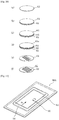
- FIG. 1 is an exploded perspective view of physical quantity sensor 100 according to the embodiment of the present disclosure.
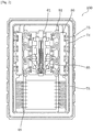
- FIG. 2 is a top view illustrating physical quantity sensor 100 in a state where lid 89 is removed.
- FIG. 3 is a bottom view of physical quantity sensor 100.
- FIG. 4 is a perspective view of detection element 61 included in physical quantity sensor 100.
- FIG. 5 is a cross-sectional side surface of detection element 61 included in physical quantity sensor 100.
- FIG. 6 is a perspective view illustrating a state where detection element 61 and terminals 81 are fixed to mount component 80 included in physical quantity sensor100.
- FIG. 7 is a perspective view of lid 89 included in physical quantity sensor 100, in a bottom view.
- FIG. 8 illustrates lid 89 included in physical quantity sensor 100, in a top view.
- FIG. 9 illustrates a cross-sectional side surface of lid 89 included in physical quantity sensor 100.
- physical quantity sensor 100 includes detection element 61, integrated circuit (IC) 88, case 70, and lid 89.
- IC integrated circuit
- detection element 61 is a detection element having a shape of a tuning fork. As illustrated in FIG. 4 , detection element 61 includes first arm 61a, second arm 61b, support portion 61c which connects one end of first arm 61a and one end of second arm 61b.
- detection element 61 includes: base 62 made of Si; common GND electrode 63 which is disposed on an upper surface of base 62 to extend over the whole surface of the upper surface of base 62, and is made of an alloy thin film of Pt and Ti; and piezoelectric layer 64 made of a PZT thin film.
- detection element 61 includes a pair of first drive electrodes 65, a pair of second drive electrodes 66, a pair of detection electrodes 67, monitor electrode 68, and ground (GND) electrode 69.
- the pair of first drive electrodes 65 is located in an inner position of approximately the center of an upper surface of detection element 61, and disposed on an upper surface of piezoelectric layer 64 as illustrated in FIG. 5 .
- the pair of second drive electrodes 66 is located in an outer position of approximately the center of the upper surface of detection element 61, and disposed on the upper surface of piezoelectric layer 64 as illustrated in FIG. 5 .
- the pair of detection electrodes 67 is located at a tip end side of the upper surface of detection element 61, and disposed on the upper surface of piezoelectric layer 64.
- Monitor electrode 68 is located closer to a root side of the upper surface of detection element 61 than first drive electrodes 65, and disposed on the upper surface of piezoelectric layer 64.
- GND electrode 69 is located at a surface of support portion 61c of detection element 61, and disposed on the surface of piezoelectric layer 64.
- Case 70 is a casing body made of a ceramic, and houses detection element 61 and IC 88. Case 70 has a substantially rectangular parallelepiped shape and has an opening of a substantially rectangular shape. In a top view, case 70 has a substantially rectangular shape. Case 70 has an inner bottom surface, inner side surfaces, and an outer bottom surface, which have a layered structure including a ceramic and a wiring conductor. As illustrated in FIG. 1 , case 70 includes multi-layer circuit board 72 having a wiring pattern (not illustrated). In addition, as illustrated in FIG. 1 and FIG. 2 , stepped portion 74 is formed in an inner side surface of side wall 73 of case 70, and terminal electrode 75 is disposed on stepped portion 74. Furthermore, as illustrated in FIG.
- power electrode 76, GND electrode 77, and output electrode 78 are disposed on an outer bottom surface of case 70.
- Terminal electrode 75 disposed on the inner side surface of case 70 is electrically connected by the wiring pattern (not illustrated) to power electrode 76, GND electrode 77, and output electrode 78 which are disposed on the outer bottom surface of case 70.
- metal frame 79 made of kovar is disposed on the upper surface of side wall 43 of case 70.
- Metal frame 79 is a frame body having a substantially rectangular shape, disposed on a frame-shaped edge portion of the opening of case 70, and fixed to the opening of case 70.
- Metal frame 79 has joint portion 79a.
- Joint portion 79a is a portion in the upper surface of metal frame 79 for joining to lid 89.
- physical quantity sensor 100 further includes mount component 80 made of resin.
- mount component 80 supports support portion 61c of detection element 61, and is supported from outside by eight terminals 81 each having one end electrically connected to terminal electrode 75 of case 70.
- Each of the eight terminals 81 includes Y-axis-direction protrusion 82, Z-axis-direction protrusion 83, and X-axis-direction protrusion 84.
- the center of gravity of mount component 80 substantially matches to the center of gravity of a combination of the eight terminals 81.
- Each of first drive electrodes 65, second drive electrodes 66, detection electrodes 67, and GND electrode 69 of detection element 61 is electrically connected to a corresponding one of terminals 81 via wire 85 as illustrated in FIG. 2 .
- physical quantity sensor 100 further includes reinforcement member 86 made of resin. As illustrated in FIG. 2 , reinforcement member 86 is disposed to cover a connecting portion between terminals 81 and terminal electrodes 75 of case 70. In this manner, by provided reinforcement member 86, terminals 81 are buried in case 70.
- physical quantity sensor 100 further includes acceleration sensor element 87.
- Acceleration sensor element 87 is disposed on the inner bottom surface of case 70. Acceleration sensor element 87 and each of terminal electrodes 75 are electrically connected to each other via wire line 85.
- IC 88 illustrated in FIG. 1 processes an output signal provided by detection electrodes 67 of detection element 61. More specifically, IC 88 is disposed in parallel with acceleration sensor element 87 in the inner bottom surface of case 70, and processes an output signal provided by detection element 61 and an output signal provided by acceleration sensor element 87.
- Lid 89 is a lid member made of kovar. Lid 89 occludes the opening of case 70. Lid 89 has a plate-like rectangular parallelepiped shape, and substantially rectangle in a plan view as illustrated in FIG. 7 and FIG. 8 . Lid 89 is joined to metal frame 79. As illustrated in FIG. 7 , lid 89 includes joint portion 90. Joint portion 90 is a portion of the surface of lid 89 for joining to metal frame 79, and lid 89 is joined at joint portion 79a of metal frame 79. According to the present embodiment, joint portion 90 of lid 89 and joint portion 79a of metal frame 79 are matched. Lid 89 and metal frame 79 can be joined by, for example, welding such as seam welding. It is possible to easily assemble physical quantity sensor 100 by joining lid 89 and metal frame 79 using seam welding.
- lid 89 includes bent portion 91.
- bent portion 91 is formed in a more interior position on lid 89 than joint portion 90 corresponding to only a longitudinal side (side in the longitudinal direction) among sides of lid 89 which are joined to metal frame 79, and along joint portion 90 corresponding to only the longitudinal side.
- bent portion 91 is formed in a more interior position on lid 89 than joint portion 90 to linearly extend along the longitudinal side of lid 89.
- bent portion 91 is formed by changing a shape of a portion of lid 89 to protrude. Bent portion 91 can be formed by, for example, press working such as drawing. It is possible to easily form bent portion 91 by forming bent portion 91 by drawing.
- FIG. 10 illustrates a process drawing for explaining a method of manufacturing detection element 61 included in physical quantity sensor 100.
- base 62 made of Si is prepared in advance as illustrated in FIG. 10(a) , and common GND electrode 63 made of an alloy thin film of Pt and Ti is formed by vapor deposition on an upper surface of base 62 as illustrated in FIG. 10(b) .
- piezoelectric layer 64 made of a PZT thin film is formed by vapor deposition on an upper surface of common GND electrode 63.
- mid-formation electrode 65a made of an alloy thin film of Ti and Au is formed by vapor deposition on an upper surface of piezoelectric layer 64 as illustrated in FIG. 10(d) .
- unnecessary portions are removed from common GND electrode 63, piezoelectric layer 64, and mid-formation electrode 65a so as to obtain a predetermined shape, thereby forming first drive electrode 65, second drive electrode 66, detection electrode 67, monitor electrode 68, and GND electrode 69 on the upper surface of piezoelectric layer 64.
- first drive electrode 65, second drive electrode 66, detection electrode 67, monitor electrode 68, and GND electrode 69 are grounded, thereby polarizing piezoelectric layer 64.
- side wall 73 and stepped portion 74 which are made of ceramics are formed to extend over the circumference of an upper surface of multi-layer circuit board 72 including an insulation body (not illustrated) made of ceramics prepared in advance and wiring conductor (not illustrated).
- terminal electrode 75 made of Au is disposed on an upper surface of stepped portion 74 of case 70, and further, metal frame 79 made of kovar is fixed to an upper surface of side wall 73.
- power electrode 76, GND electrode 77, and output electrode 78 each made of Ag are disposed on the bottom surface of multi-layer circuit board 72.
- IC 88 is mounted on the upper surface of multi-layer circuit board 72 of case 70, and then IC 88 and multi-layer circuit board 72 are electrically connected to each other.
- acceleration sensor element 87 is mounted on the upper surface of multi-layer circuit board 72 of case 70 to be in parallel with IC 88, and then acceleration sensor element 87 and each of terminal electrodes 75 included in case 70 are electrically connected by wire bonding to each other via wire line 85 made of aluminum.
- first drive electrodes 65, second drive electrodes 66, detection electrodes 67, monitor electrode 68, and GND electrode 69 which are disposed on the upper surface of detection element 61 are each electrically connected by wire bonding to a corresponding one of terminals 81 via wire line made of aluminum.
- terminals 81 are buried in case 70 by covering terminals 81 by reinforcement member 86 made of resin.
- bent portion 92 is formed by deep drawing in a more interior position on lid 89 than joint portion 90 corresponding to only the longitudinal side of lid 89 made of metal which is prepared in advance.
- metal frame 79 included in case 70 and lid 89 are fixed by joining lid 89 by seam welding to the opening of case 70 in a nitrogen atmosphere.
- lid 89 and metal frame 79 When joining lid 89 and metal frame 79 by the seam welding, Joule heat is generated by supplying current to lid 89, and the connecting portion of lid 89 made of the alloy of Fe, Ni, and Co and metal frame 79 is heated to the melting point of 1449 degrees Celsius to be melted. Lid 89 is pressed toward case 70 while the connecting portion is melted, thereby connecting case 70 and lid 89 with each other. In this manner, it is possible to assemble physical quantity sensor 100. At this time, the temperature of lid 89 as a whole increases to approximately 700 degrees Celsius on average.
- lid 89 shrinks when the temperature of physical quantity sensor 100 decreases to room temperature. At this time, since tensile stress is applied by lid 89 to the outer surface of case 70, there is a possibility of cracking in the outer surface of case 70 unless bent portion 92 is formed in a position corresponding to only the longitudinal side of lid 89.
- ⁇ e 4.75 ⁇ 10 8 [Pa] in the case where bent portion 92 is not formed.
- ⁇ e ⁇ 1 2 ⁇ ⁇ 1 ⁇ ⁇ 2 + ⁇ 2 2
- bent portion 92 having a shape of a frame is considered as a method of alleviating the tensile stress generated in lid 89. More specifically, as illustrated in FIG. 11 , bent portion 92 has a shape including a curve that protrudes downward from lid 89X, and is formed in a more interior position on lid 89X than joint portion 90 of lid 89X for joining to metal frame 79 to extend over the whole circumference of joint portion 90, and along joint portion 90 of lid 89X.
- lid 89X has a rectangular shape in a top view
- the Von Mises stress ⁇ e that is represented by a scalar value increases as a result of forming bent portion 92 in a shape of a frame to extend over the whole circumference of joint portion 90, causing an adverse effect on alleviation of stress.
- bent portion 91 is formed in a more interior position on lid 89 than joint portion 90 corresponding to only a longitudinal side among the sides of lid 89 which are joined to metal frame 79 and along joint portion 90 corresponding to only the longitudinal side.
- bent portion 91 of lid 89 according to the embodiment does not include short-side bent portion 93 unlike bent portion 92 of lid 89X illustrated in FIG. 11 , the tensile stress ( ⁇ 2 ) applied to the short-side area is not significantly reduced in lid 89 according to the embodiment.
- the Von Mises stress ⁇ e generated in lid 89 works as shear forces to side wall 73 of case 70.
- the tensile stress applied to side wall 73 of case 70 is 7.09 ⁇ 10 7 [Pa] as a result of calculating the tensile stress by simulation. Accordingly, the tensile stress is significantly reduced compared to the case where bent portion 92 is formed to extend over the whole circumference.
- bent portion 91 is formed in a more interior position on lid 89 than joint portion 90 corresponding to only a longitudinal side, in a top view, among the sides of lid 89 which are joined to metal frame 79, and along joint portion 90 corresponding to only the longitudinal side. Accordingly, the tensile stress ⁇ 2 applied to the short-side area of lid 89 is not significantly reduced.
- the von Mises stress that is represented by a scalar value does not increase, and thus it is possible to suppress concentration of stress to and around the center portion of the longitudinal-side area of the outer surface of case 70 joined to lid 89 via metal frame 79.
- first arm 61a of detection element 61 having a shape of a tuning fork and first drive electrodes 65 disposed on first arm 61a
- a negative voltage is applied to second drive electrodes 66.
- This causes piezoelectric layer 64 under first drive electrodes 65 to stretch, and piezoelectric layer 64 under second drive electrodes 66 to shrink.
- first arm 61a and second arm 61b of detection element 61 move outwardly away from each other.
- first arm 61a of detection element 61 having a shape of a tuning fork and first drive electrodes 65 disposed on first arm 61a
- a positive voltage is applied to second drive electrodes 66.
- This causes piezoelectric layer 64 under first drive electrodes 65 to shrink, and piezoelectric layer 64 under second drive electrodes 66 to stretch.
- first arm 61a and second arm 61b of detection element 61 move inwardly to come close to each other.
- first drive electrodes 65 and second drive electrodes 66 of detection element 61 having a shape of a tuning fork
- first arm 61a and second arm 61b of detection element 61 perform bending movement at velocity V at natural frequency in an in-plane direction.
- voltages applied to first drive electrodes 65 and second drive electrodes 66 are adjusted so as to maintain an output signal generated from monitor electrode 68 to be constant, thereby controlling the amplitude of the bending vibration.
- first arm 61a and second arm 61b of detection element 61 perform bending movement at natural frequency
- the Coriolis force of F 2mV ⁇ ⁇
- the Coriolis force causes an output signal corresponding to a charge generated in piezoelectric layer 64 under detection electrodes 67 to be input to IC 88 via detection electrodes 67, wire 85, terminal electrodes 75, and wiring pattern (not illustrated) of case 70.
- the output signal is subject to waveform processing, and then output from output electrode 78 of case 70 to the outside, as an output signal at an angular velocity.
- bent portion 91 which has a linear shape is formed in lid 89 in physical quantity sensor 100 according to the above-described embodiment
- shape of the bent portion is not limited to this example.
- lid 89A including bent portion 94 having a rhomboid shape in a top view as illustrated in FIG. 12 is also capable of producing the same advantageous effect.
- the physical quantity sensor according to the present disclosure produces an advantageous effect that it is possible to suppress cracking in the outer surface in the longitudinal-side area of the case even when the lid has a rectangular shape in a top view, and is particularly useful as a physical quantity sensor used in attitude control, a navigation system, etc., for mobile objects such as aircrafts, vehicles, etc.
Landscapes
- Engineering & Computer Science (AREA)
- Microelectronics & Electronic Packaging (AREA)
- Physics & Mathematics (AREA)
- General Physics & Mathematics (AREA)
- Radar, Positioning & Navigation (AREA)
- Remote Sensing (AREA)
- Gyroscopes (AREA)
- Piezo-Electric Or Mechanical Vibrators, Or Delay Or Filter Circuits (AREA)
- Pressure Sensors (AREA)
Description
- The present disclosure relates to physical quantity sensors, and particularly to a physical quantity sensor for use in attitude control, a navigation system, etc., for mobile objects such as aircrafts, vehicles, etc.
- Conventionally known such physical quantity sensors include a gyroscope, etc. Conventional physical quantity sensors have a configuration as illustrated in
FIG. 13 and FIG. 14 for suppressing cracking due to concentration of stress approximately at the center portion of an outer surface of a case. -
FIG. 13 illustrates a cross-sectional side surface of a conventional physical quantity sensor.FIG. 14 illustrates a lid of the conventional physical quantity sensor in a top view. - As illustrated in
FIG. 13 and FIG. 14 , the conventional physical quantity sensor includes integrated circuit (IC) 1 andcase 2. InIC 1, a detection element (not illustrated) such as a piezoelectric vibrator is disposed.IC 1 processes an output signal from the detection element.Case 2 is made of glass ceramics, for example, and housesIC 1. -
Case 2 includes power electrode 3,output electrode 4, and a ground (GND) electrode (not illustrated), on an outer bottom surface. Power electrode 3,output electrode 4, and the GND electrode (not illustrated) are electrically connected toIC 1 and the detection element (not illustrated) viawiring conductor 5 andlead 6. In addition,metallization layer 7 is disposed on an upper surface ofcase 2. - Metal frame 8 is disposed on
metallization layer 7. Metal frame 8 is made of, for example, an alloy of Fe, Ni, and Co, and is brazed tometallization layer 7.Lid 9 is disposed on metal frame 8.Lid 9 is made of, for example, an alloy of Fe, Ni, and Co, and is joined to metal frame 8 by brazing, for example. As illustrated inFIG. 14 ,lid 9 has a shape of square parallelepiped in a top view. - Bent
portion 10 is formed inlid 9.Bent portion 10 has a shape curved to protrude downward, and is formed in a more interior position onlid 9 thanjoint portion 11 between metal frame 8 andlid 9, and alongjoint portion 11 to extend over the whole circumference oflid 9. - The following describes, in particular, a method of attaching
lid 9 tocase 2 of the conventional physical quantity sensor configured as described above. - First, Joule heat is generated by supplying current via metal frame 8 to
lid 9 disposed in an opening ofcase 2, and a connecting portion oflid 9 made of the alloy of Fe, Ni, and Co is heated to the melting point of 1449 degrees Celsius to be melted. Next,lid 9 is pressed towardcase 2 to connectcase 2 andlid 9 with each other. At this time, the temperature oflid 9 as a whole increases to approximately 700 degrees Celsius on average. - Subsequently,
lid 9 shrinks when the temperature of the physical quantity sensor decreases to room temperature. At this time, there are instances where a crack appears in the outer surface ofcase 2 due to tensile stress applied to the outer surface ofcase 2 as a result of shrinking oflid 9. - For that reason, the conventional physical quantity sensor has
bent portion 10 inlid 9. In this manner, even iflid 9 shrinks,bent portion 10 bends to reduce the tensile stress applied to the outer surface ofcase 2, and thus it is possible to suppress cracking in the outer surface ofcase 2. -
Bent portion 10, as described above, is formed in a more interior position onlid 9 thanjoint portion 11 between metal frame 8 andlid 9, and alongjoint portion 11 to extend over the whole circumference oflid 9. For this reason, inlid 9 having a square shape in a top view, it is possible to uniformly reduce the tensile stress that is generated in four sides oflid 9. - For example, Patent Literature (PTL) 1 and 2 are known as information on background art documents related to the disclosure of this application.
-
- [PTL 1] Japanese Unexamined Patent Application Publication No.
2006-332599 - [PTL 2]
WO 2015/075908 A1 - However, in the case where
lid 9 of the above-described conventional physical quantity sensor has a rectangular shape in a top view, whenbent portion 10 is formed in a more interior position onlid 9 thanjoint portion 11 between metal frame 8 andlid 9, and alongjoint portion 11 to extend over the whole circumference oflid 9, the tensile stress applied to short-side areas oflid 9 is significantly reduced due tobent portion 10 formed in the short-side areas oflid 9. As a result, von Mises stress that is represented by a scalar value increases. Accordingly, stress concentrates approximately at the center portions of longitudinal-side areas of the outer surface ofcase 2 which correspond to longitudinal-side areas oflid 9, posing a problem that it is difficult to suppress cracking in the outer surface ofcase 2. - The present disclosure provides a solution to the problems described above. One non-limiting and explanatory embodiment provides a physical quantity sensor capable of suppressing cracking in the outer surface of a case, even when a lid has a rectangular shape in a top view.
- In order to achieve the above-described object, the present disclosure has a configuration as described below.
- The physical quantity sensor according to the invention includes: a detection element including a drive electrode and a detection electrode; an integrated circuit (IC) which processes an output signal provided by the detection electrode; a case which has an opening, and houses the detection element and the IC; a lid which has a rectangular parallelepiped shape, and occludes the opening of the case; a power electrode, a ground (GND) electrode), and an output electrode, which are disposed on an outer bottom surface of the case; and a metal frame disposed on an upper surface of the case. The lid is joined to the metal frame, and includes two bent portions formed by changing the shape of a portion of the lid to protrude in a more interior position on the lid than a joint portion corresponding to only a longitudinal side, in a top view, among sides of the lid which are joined to the metal frame, and along the joint portion corresponding to only the longitudinal side.
- According to this configuration, the lid includes the bent portion formed in a more interior position on the lid than the joint portion corresponding to only the longitudinal side among the sides of the lid which are joined to the metal frame, and along the joint portion corresponding to only the longitudinal side, thereby preventing significant reduction in the tensile stress applied to short-side areas of the lid. As a result, the von Mises stress that is represented by a scalar value does not increase, and thus it is possible to suppress concentration of stress approximately at the center portions of the longitudinal-side areas of the outer surface of the case joined to the lid via the metal frame.
- In addition, according to an aspect of the physical quantity sensor of the present disclosure, the bent portion may be formed by drawing.
- According to this configuration, it is possible to easily form the bent portion.
- In addition, according to an aspect of the physical quantity sensor of the present disclosure, the metal frame and the lid may be joined by seam welding.
- According to this configuration, it is possible to easily assemble the physical quantity sensor.
- According to the present disclosure, it is possible to suppress cracking in an outer surface of a case even when a lid has a rectangular shape in a top view.
-
-
FIG. 1 is an exploded perspective view of a physical quantity sensor according to an embodiment of the present disclosure. -
FIG. 2 is a top view illustrating the physical quantity sensor according to the embodiment, in a state where a lid is removed. -
FIG. 3 is a bottom view of the physical quantity sensor according to the embodiment of the present disclosure. -
FIG. 4 is a perspective view of a detection element included in the physical quantity sensor according to the embodiment of the present disclosure. -
FIG. 5 illustrates a cross-sectional side surface of the detection element included in the physical quantity sensor according to the embodiment of the present disclosure. -
FIG. 6 is a perspective view illustrating a state where the detection element and terminals are fixed to a mount component included in the physical quantity sensor according to the embodiment of the present disclosure. -
FIG. 7 is a perspective view of the lid of the physical quantity sensor according to the embodiment of the present disclosure, in a bottom view. -
FIG. 8 illustrates the lid of the physical quantity sensor according to the embodiment of the present disclosure, in a top view. -
FIG. 9 illustrates a cross-sectional side surface of the lid included in the physical quantity sensor according to the embodiment of the present disclosure. -
FIG. 10 illustrates a process drawing for explaining a method of manufacturing the detection element included in the physical quantity sensor according to the embodiment of the present disclosure. -
FIG. 11 is a perspective view of a lid included in a physical quantity sensor of a comparison example, in a bottom view. -
FIG. 12 illustrates the lid of the physical quantity sensor according to a modification example of the present disclosure, in a top view. -
FIG. 13 illustrates a cross-sectional side surface of a conventional physical quantity sensor. -
FIG. 14 illustrates the lid of the conventional physical quantity sensor in a top view. - Hereinafter, an embodiment of the present disclosure shall be described with reference to the drawings. It should be noted that the subsequently-described embodiment shows a specific example of the present disclosure. Thus, the numerical values, shapes, materials, structural components, the disposition and connection of the structural components, and others described in the following embodiment are mere examples, and do not intend to limit the present disclosure. Furthermore, among the structural components in the following embodiment, components not recited in the independent claim which indicates the broadest concept of the present disclosure are described as arbitrary structural components.
- In addition, each of the diagrams is a pattern diagram and thus is not necessarily strictly illustrated. In each of the diagrams, substantially the same structural components are assigned with the same reference signs, and redundant descriptions will be omitted or simplified. Furthermore, axis X, axis Y, and axis Z represent three axes of a three-dimensional orthogonal coordinate system in the Description and Drawings of the present application.
- First, a configuration of
physical quantity sensor 100 according to the embodiment of the present disclosure shall be described with reference toFIG. 1 to FIG. 9 . -
FIG. 1 is an exploded perspective view ofphysical quantity sensor 100 according to the embodiment of the present disclosure.FIG. 2 is a top view illustratingphysical quantity sensor 100 in a state wherelid 89 is removed.FIG. 3 is a bottom view ofphysical quantity sensor 100.FIG. 4 is a perspective view ofdetection element 61 included inphysical quantity sensor 100.FIG. 5 is a cross-sectional side surface ofdetection element 61 included inphysical quantity sensor 100.FIG. 6 is a perspective view illustrating a state wheredetection element 61 andterminals 81 are fixed to mountcomponent 80 included in physical quantity sensor100.FIG. 7 is a perspective view oflid 89 included inphysical quantity sensor 100, in a bottom view.FIG. 8 illustrateslid 89 included inphysical quantity sensor 100, in a top view.FIG. 9 illustrates a cross-sectional side surface oflid 89 included inphysical quantity sensor 100. - As illustrated in
FIG. 1 ,physical quantity sensor 100 includesdetection element 61, integrated circuit (IC) 88,case 70, andlid 89. - As illustrated in
FIG. 1 ,FIG. 2 , andFIG. 4 ,detection element 61 is a detection element having a shape of a tuning fork. As illustrated inFIG. 4 ,detection element 61 includesfirst arm 61a,second arm 61b,support portion 61c which connects one end offirst arm 61a and one end ofsecond arm 61b. - In addition, as illustrated in
FIG. 5 ,detection element 61 includes:base 62 made of Si;common GND electrode 63 which is disposed on an upper surface ofbase 62 to extend over the whole surface of the upper surface ofbase 62, and is made of an alloy thin film of Pt and Ti; andpiezoelectric layer 64 made of a PZT thin film. - Furthermore, as illustrated in
FIG. 4 ,detection element 61 includes a pair offirst drive electrodes 65, a pair ofsecond drive electrodes 66, a pair ofdetection electrodes 67,monitor electrode 68, and ground (GND)electrode 69. - The pair of
first drive electrodes 65 is located in an inner position of approximately the center of an upper surface ofdetection element 61, and disposed on an upper surface ofpiezoelectric layer 64 as illustrated inFIG. 5 . The pair ofsecond drive electrodes 66 is located in an outer position of approximately the center of the upper surface ofdetection element 61, and disposed on the upper surface ofpiezoelectric layer 64 as illustrated inFIG. 5 . The pair ofdetection electrodes 67 is located at a tip end side of the upper surface ofdetection element 61, and disposed on the upper surface ofpiezoelectric layer 64.Monitor electrode 68 is located closer to a root side of the upper surface ofdetection element 61 thanfirst drive electrodes 65, and disposed on the upper surface ofpiezoelectric layer 64.GND electrode 69 is located at a surface ofsupport portion 61c ofdetection element 61, and disposed on the surface ofpiezoelectric layer 64. -
Case 70 is a casing body made of a ceramic, and housesdetection element 61 andIC 88.Case 70 has a substantially rectangular parallelepiped shape and has an opening of a substantially rectangular shape. In a top view,case 70 has a substantially rectangular shape.Case 70 has an inner bottom surface, inner side surfaces, and an outer bottom surface, which have a layered structure including a ceramic and a wiring conductor. As illustrated inFIG. 1 ,case 70 includesmulti-layer circuit board 72 having a wiring pattern (not illustrated). In addition, as illustrated inFIG. 1 andFIG. 2 , steppedportion 74 is formed in an inner side surface ofside wall 73 ofcase 70, andterminal electrode 75 is disposed on steppedportion 74. Furthermore, as illustrated inFIG. 3 ,power electrode 76,GND electrode 77, andoutput electrode 78 are disposed on an outer bottom surface ofcase 70.Terminal electrode 75 disposed on the inner side surface ofcase 70 is electrically connected by the wiring pattern (not illustrated) topower electrode 76,GND electrode 77, andoutput electrode 78 which are disposed on the outer bottom surface ofcase 70. - As illustrated in
FIG. 1 ,metal frame 79 made of kovar is disposed on the upper surface of side wall 43 ofcase 70.Metal frame 79 is a frame body having a substantially rectangular shape, disposed on a frame-shaped edge portion of the opening ofcase 70, and fixed to the opening ofcase 70.Metal frame 79 hasjoint portion 79a.Joint portion 79a is a portion in the upper surface ofmetal frame 79 for joining tolid 89. - As illustrated in
FIG. 1 ,physical quantity sensor 100 further includesmount component 80 made of resin. As illustrated inFIG. 6 ,mount component 80 supports supportportion 61c ofdetection element 61, and is supported from outside by eightterminals 81 each having one end electrically connected toterminal electrode 75 ofcase 70. Each of the eightterminals 81 includes Y-axis-direction protrusion 82, Z-axis-direction protrusion 83, and X-axis-direction protrusion 84. Among the eightterminals 81, fourterminals 81 disposed on the outer side each have X-axis-direction protrusion 84 that protrudes toward the front side, and fourterminals 81 disposed on the inner side each have X-axis-direction protrusion 84 that protrudes toward the rear side. In other words, the center of gravity ofmount component 80 substantially matches to the center of gravity of a combination of the eightterminals 81. - Each of
first drive electrodes 65,second drive electrodes 66,detection electrodes 67, andGND electrode 69 ofdetection element 61 is electrically connected to a corresponding one ofterminals 81 viawire 85 as illustrated inFIG. 2 . - As illustrated in
FIG. 2 andFIG. 6 ,physical quantity sensor 100 further includesreinforcement member 86 made of resin. As illustrated inFIG. 2 ,reinforcement member 86 is disposed to cover a connecting portion betweenterminals 81 andterminal electrodes 75 ofcase 70. In this manner, by providedreinforcement member 86,terminals 81 are buried incase 70. - As illustrated in
FIG. 1 ,physical quantity sensor 100 further includesacceleration sensor element 87.Acceleration sensor element 87 is disposed on the inner bottom surface ofcase 70.Acceleration sensor element 87 and each ofterminal electrodes 75 are electrically connected to each other viawire line 85. -
IC 88 illustrated inFIG. 1 processes an output signal provided bydetection electrodes 67 ofdetection element 61. More specifically,IC 88 is disposed in parallel withacceleration sensor element 87 in the inner bottom surface ofcase 70, and processes an output signal provided bydetection element 61 and an output signal provided byacceleration sensor element 87. -
Lid 89 is a lid member made of kovar.Lid 89 occludes the opening ofcase 70.Lid 89 has a plate-like rectangular parallelepiped shape, and substantially rectangle in a plan view as illustrated inFIG. 7 andFIG. 8 .Lid 89 is joined tometal frame 79. As illustrated inFIG. 7 ,lid 89 includesjoint portion 90.Joint portion 90 is a portion of the surface oflid 89 for joining tometal frame 79, andlid 89 is joined atjoint portion 79a ofmetal frame 79. According to the present embodiment,joint portion 90 oflid 89 andjoint portion 79a ofmetal frame 79 are matched.Lid 89 andmetal frame 79 can be joined by, for example, welding such as seam welding. It is possible to easily assemblephysical quantity sensor 100 by joininglid 89 andmetal frame 79 using seam welding. - As illustrated in
FIG. 7 to FIG. 9 ,lid 89 includesbent portion 91. As illustrated inFIG. 7 , in a top view,bent portion 91 is formed in a more interior position onlid 89 thanjoint portion 90 corresponding to only a longitudinal side (side in the longitudinal direction) among sides oflid 89 which are joined tometal frame 79, and alongjoint portion 90 corresponding to only the longitudinal side. In other words, as illustrated inFIG. 7 andFIG. 8 ,bent portion 91 is formed in a more interior position onlid 89 thanjoint portion 90 to linearly extend along the longitudinal side oflid 89. In addition, as illustrated inFIG. 9 ,bent portion 91 is formed by changing a shape of a portion oflid 89 to protrude.Bent portion 91 can be formed by, for example, press working such as drawing. It is possible to easily formbent portion 91 by formingbent portion 91 by drawing. - The following describes, using
FIG. 10 , a method of assemblingphysical quantity sensor 100 that is configured as described above, with reference toFIG. 1 .FIG. 10 illustrates a process drawing for explaining a method ofmanufacturing detection element 61 included inphysical quantity sensor 100. - First,
base 62 made of Si is prepared in advance as illustrated inFIG. 10(a) , andcommon GND electrode 63 made of an alloy thin film of Pt and Ti is formed by vapor deposition on an upper surface ofbase 62 as illustrated inFIG. 10(b) . Subsequently, as illustrated inFIG. 10(c) ,piezoelectric layer 64 made of a PZT thin film is formed by vapor deposition on an upper surface ofcommon GND electrode 63. - Then,
mid-formation electrode 65a made of an alloy thin film of Ti and Au is formed by vapor deposition on an upper surface ofpiezoelectric layer 64 as illustrated inFIG. 10(d) . Subsequently, as illustrated inFIG. 10(e) , unnecessary portions are removed fromcommon GND electrode 63,piezoelectric layer 64, andmid-formation electrode 65a so as to obtain a predetermined shape, thereby formingfirst drive electrode 65,second drive electrode 66,detection electrode 67,monitor electrode 68, andGND electrode 69 on the upper surface ofpiezoelectric layer 64. - Next, although not illustrated, a voltage is applied to
common GND electrode 63, andfirst drive electrode 65,second drive electrode 66,detection electrode 67,monitor electrode 68, andGND electrode 69 are grounded, thereby polarizingpiezoelectric layer 64. - Next, an unnecessary portion is removed from
base material 62, thereby formingindividual detection element 61 as illustrated inFIG. 10(f) . - Next, as illustrated in
FIG. 1 ,side wall 73 and steppedportion 74 which are made of ceramics are formed to extend over the circumference of an upper surface ofmulti-layer circuit board 72 including an insulation body (not illustrated) made of ceramics prepared in advance and wiring conductor (not illustrated). Subsequently,terminal electrode 75 made of Au is disposed on an upper surface of steppedportion 74 ofcase 70, and further,metal frame 79 made of kovar is fixed to an upper surface ofside wall 73. - Next,
power electrode 76,GND electrode 77, andoutput electrode 78 each made of Ag are disposed on the bottom surface ofmulti-layer circuit board 72. - Next,
IC 88 is mounted on the upper surface ofmulti-layer circuit board 72 ofcase 70, and thenIC 88 andmulti-layer circuit board 72 are electrically connected to each other. - Next,
acceleration sensor element 87 is mounted on the upper surface ofmulti-layer circuit board 72 ofcase 70 to be in parallel withIC 88, and thenacceleration sensor element 87 and each ofterminal electrodes 75 included incase 70 are electrically connected by wire bonding to each other viawire line 85 made of aluminum. - Next, subsequent to mounting the eight
terminals 81 onmount component 80 by insert molding in advance, a bottom surface ofsupport portion 61c included indetection element 61 is fixed to mountcomponent 80. Then,first drive electrodes 65,second drive electrodes 66,detection electrodes 67,monitor electrode 68, andGND electrode 69 which are disposed on the upper surface ofdetection element 61 are each electrically connected by wire bonding to a corresponding one ofterminals 81 via wire line made of aluminum. - Next, subsequent to soldering the eight
terminals 81 toterminal electrodes 75 included incase 70,terminals 81 are buried incase 70 by coveringterminals 81 byreinforcement member 86 made of resin. - Next,
bent portion 92 is formed by deep drawing in a more interior position onlid 89 thanjoint portion 90 corresponding to only the longitudinal side oflid 89 made of metal which is prepared in advance. - Lastly,
metal frame 79 included incase 70 andlid 89 are fixed by joininglid 89 by seam welding to the opening ofcase 70 in a nitrogen atmosphere. - The following describes a state in which
lid 89 having a rectangular shape in a top view as in the present embodiment shrinks due to the seam welding at this time. - When joining
lid 89 andmetal frame 79 by the seam welding, Joule heat is generated by supplying current tolid 89, and the connecting portion oflid 89 made of the alloy of Fe, Ni, and Co andmetal frame 79 is heated to the melting point of 1449 degrees Celsius to be melted.Lid 89 is pressed towardcase 70 while the connecting portion is melted, thereby connectingcase 70 andlid 89 with each other. In this manner, it is possible to assemblephysical quantity sensor 100. At this time, the temperature oflid 89 as a whole increases to approximately 700 degrees Celsius on average. - Subsequently,
lid 89 shrinks when the temperature ofphysical quantity sensor 100 decreases to room temperature. At this time, since tensile stress is applied bylid 89 to the outer surface ofcase 70, there is a possibility of cracking in the outer surface ofcase 70 unlessbent portion 92 is formed in a position corresponding to only the longitudinal side oflid 89. - Here, when the tensile stress applied to longitudinal-side area of
lid 89 is σ1 and the tensile stress applied to short-side area oflid 89 is σ2 as illustrated inFIG. 7 , calculating σ1 and σ2 by simulation results in σ1 = 4.90 × 10⁸ [Pa], and σ2 = 4.58 × 10⁸ [Pa] in the case wherebent portion 92 is not formed inlid 89. - For that reason, the von Mises stress σe represented by the expression below is σe = 4.75 × 10⁸ [Pa] in the case where
bent portion 92 is not formed.
- σe: the Von Mises stress applied to the longitudinal side of the lid (Mpa)
- σ1: the tensile stress applied to the longitudinal side of the lid (Mpa)
- σ2: the tensile stress applied to the short side of the lid (Mpa)
- In view of the above, as illustrated in
FIG. 11 , the case wherebent portion 92 having a shape of a frame is formed inlid 89X is considered as a method of alleviating the tensile stress generated inlid 89. More specifically, as illustrated inFIG. 11 ,bent portion 92 has a shape including a curve that protrudes downward fromlid 89X, and is formed in a more interior position onlid 89X thanjoint portion 90 oflid 89X for joining tometal frame 79 to extend over the whole circumference ofjoint portion 90, and alongjoint portion 90 oflid 89X. - When σ1 and σ2 generated in
lid 89X illustrated inFIG. 11 are calculated in the same manner as above, the calculation results in σ1 = 5.30 × 10⁸ [Pa], and σ2 = 3.81 × 10⁸ [Pa]. In other words, tensile stress σ2 generated in an interior position ofbent portion 92 is significantly reduced by short-sidebent portion 93 formed in the short-side area ofbent portion 92. In this case, the Von Mises stress σe represented by the above-described expression is σe = 5.18 × 10⁸ [Pa]. - More specifically, when
lid 89X has a rectangular shape in a top view, the Von Mises stress σe that is represented by a scalar value increases as a result of formingbent portion 92 in a shape of a frame to extend over the whole circumference ofjoint portion 90, causing an adverse effect on alleviation of stress. - The above-described Von Mises stress σe works as shear forces to
side wall 73 ofcase 70. At this time, the tensile stress is 7.55 × 10⁷ [Pa] as a result of calculating the tensile stress applied toside wall 73 ofcase 70 by simulation. - In contrast, in
physical quantity sensor 100 according to the embodiment as illustrated inFIG. 7 ,bent portion 91 is formed in a more interior position onlid 89 thanjoint portion 90 corresponding to only a longitudinal side among the sides oflid 89 which are joined tometal frame 79 and alongjoint portion 90 corresponding to only the longitudinal side. - Here, in the same manner as above, when the tensile stress applied to the longitudinal-side area of
lid 89 is σ1 and the tensile stress applied to the short-side area oflid 89 is σ2 as illustrated inFIG. 7 , calculating σ1 and σ2 by simulation results in σ1 = 4.74 × 10⁸ [Pa], and σ2 = 4.80 × 10⁸ [Pa] in the case wherebent portion 91 is formed in a more interior position onlid 89 thanjoint portion 90 corresponding to only a longitudinal side oflid 89 as described in the embodiment. - This means that, since
bent portion 91 oflid 89 according to the embodiment does not include short-sidebent portion 93 unlikebent portion 92 oflid 89X illustrated inFIG. 11 , the tensile stress (σ2) applied to the short-side area is not significantly reduced inlid 89 according to the embodiment. - For that reason, in the case where
bent portion 91 is formed forjoint portion 90 corresponding to only the longitudinal side as in the present embodiment, the Von Mises stress σe is represented by the above-described expression is σe = 4.77 × 10⁸ [Pa]. Accordingly, the Von Mises stress is significantly reduced compared to the case wherebent portion 92 is formed to extend over the whole circumference. - As described above, the Von Mises stress σe generated in
lid 89 works as shear forces toside wall 73 ofcase 70. At this time, the tensile stress applied toside wall 73 ofcase 70 is 7.09 × 10⁷ [Pa] as a result of calculating the tensile stress by simulation. Accordingly, the tensile stress is significantly reduced compared to the case wherebent portion 92 is formed to extend over the whole circumference. - In other words, in
physical quantity sensor 100 according to the embodiment,bent portion 91 is formed in a more interior position onlid 89 thanjoint portion 90 corresponding to only a longitudinal side, in a top view, among the sides oflid 89 which are joined tometal frame 79, and alongjoint portion 90 corresponding to only the longitudinal side. Accordingly, the tensile stress σ2 applied to the short-side area oflid 89 is not significantly reduced. - As a result, the von Mises stress that is represented by a scalar value does not increase, and thus it is possible to suppress concentration of stress to and around the center portion of the longitudinal-side area of the outer surface of
case 70 joined tolid 89 viametal frame 79. - The following describes operations of
physical quantity sensor 100 configured as described above according to the present embodiment. - First, a positive voltage is applied to
first arm 61a ofdetection element 61 having a shape of a tuning fork andfirst drive electrodes 65 disposed onfirst arm 61a, and a negative voltage is applied tosecond drive electrodes 66. This causespiezoelectric layer 64 underfirst drive electrodes 65 to stretch, andpiezoelectric layer 64 undersecond drive electrodes 66 to shrink. In this manner,first arm 61a andsecond arm 61b ofdetection element 61 move outwardly away from each other. - Next, a negative voltage is applied to
first arm 61a ofdetection element 61 having a shape of a tuning fork andfirst drive electrodes 65 disposed onfirst arm 61a, and a positive voltage is applied tosecond drive electrodes 66. This causespiezoelectric layer 64 underfirst drive electrodes 65 to shrink, andpiezoelectric layer 64 undersecond drive electrodes 66 to stretch. In this manner,first arm 61a andsecond arm 61b ofdetection element 61 move inwardly to come close to each other. - More specifically, when an AC voltage is applied to
first drive electrodes 65 andsecond drive electrodes 66 ofdetection element 61 having a shape of a tuning fork,first arm 61a andsecond arm 61b ofdetection element 61 perform bending movement at velocity V at natural frequency in an in-plane direction. During the bending movement indetection element 61, voltages applied tofirst drive electrodes 65 andsecond drive electrodes 66 are adjusted so as to maintain an output signal generated frommonitor electrode 68 to be constant, thereby controlling the amplitude of the bending vibration. - In the state where
first arm 61a andsecond arm 61b ofdetection element 61 perform bending movement at natural frequency, whendetection element 61 rotates about the central axis (detection axis) of longitudinal direction at an angular velocity ω, the Coriolis force of F = 2mV × ω is generated infirst arm 61a andsecond arm 61b ofdetection element 61. The Coriolis force causes an output signal corresponding to a charge generated inpiezoelectric layer 64 underdetection electrodes 67 to be input toIC 88 viadetection electrodes 67,wire 85,terminal electrodes 75, and wiring pattern (not illustrated) ofcase 70. The output signal is subject to waveform processing, and then output fromoutput electrode 78 ofcase 70 to the outside, as an output signal at an angular velocity. - Although the physical quantity sensor according to the present disclosure has been described based on the above-described embodiment, the present disclosure is not limited to the above-described embodiment.
- For example, although
bent portion 91 which has a linear shape is formed inlid 89 inphysical quantity sensor 100 according to the above-described embodiment, the shape of the bent portion is not limited to this example. For example,lid 89A includingbent portion 94 having a rhomboid shape in a top view as illustrated inFIG. 12 is also capable of producing the same advantageous effect. - The physical quantity sensor according to the present disclosure produces an advantageous effect that it is possible to suppress cracking in the outer surface in the longitudinal-side area of the case even when the lid has a rectangular shape in a top view, and is particularly useful as a physical quantity sensor used in attitude control, a navigation system, etc., for mobile objects such as aircrafts, vehicles, etc.
-
- 61 detection element
- 65, 66 drive electrode
- 67 detection electrode
- 70 case
- 76 power electrode
- 77 GND electrode
- 78 output electrode
- 79 metal frame
- 88 IC
- 89, 89A lid
- 90 joint portion
- 91, 94 bent portion
- 100 physical quantity sensor
Claims (3)
- (Amended) A physical quantity sensor (100), comprising:a detection element (61) including a drive electrode (65, 66) and a detection electrode (67);an integrated circuit (IC) (88) which processes an output signal provided by the detection electrode;a case (70) which has an opening, and houses the detection element and the IC;a lid (89, 89A) which has a rectangular parallelepiped shape, and occludes the opening of the case;a power electrode (76), a ground (GND) electrode (77), and an output electrode (78), which are disposed on an outer bottom surface of the case; and a metal frame (79) disposed on an upper surface of the case,wherein the lid is joined to the metal frame, characterized in that the lid includes two bent portions (91, 94) formed by changing a shape of a portion of the lid to protrude in a more interior position on the lid than a joint portion (90) corresponding to only a longitudinal side, in a top view, among sides of the lid which are joined to the metal frame, and along the joint portion corresponding to only the longitudinal side.
- (Amended) The physical quantity sensor according to claim 1,
wherein the two bent portions are formed by drawing. - The physical quantity sensor according to claim 1,
wherein the metal frame and the lid are joined by seam welding.
Applications Claiming Priority (2)
| Application Number | Priority Date | Filing Date | Title |
|---|---|---|---|
| JP2016004739A JP5995212B1 (en) | 2016-01-13 | 2016-01-13 | Physical quantity sensor |
| PCT/JP2017/000899 WO2017122755A1 (en) | 2016-01-13 | 2017-01-12 | Physical quantity sensor |
Publications (2)
| Publication Number | Publication Date |
|---|---|
| EP3403053A1 EP3403053A1 (en) | 2018-11-21 |
| EP3403053B1 true EP3403053B1 (en) | 2019-11-06 |
Family
ID=56960969
Family Applications (1)
| Application Number | Title | Priority Date | Filing Date |
|---|---|---|---|
| EP17704550.7A Active EP3403053B1 (en) | 2016-01-13 | 2017-01-12 | Physical quantity sensor |
Country Status (5)
| Country | Link |
|---|---|
| US (1) | US9960091B2 (en) |
| EP (1) | EP3403053B1 (en) |
| JP (1) | JP5995212B1 (en) |
| CN (1) | CN108885103B (en) |
| WO (1) | WO2017122755A1 (en) |
Family Cites Families (9)
| Publication number | Priority date | Publication date | Assignee | Title |
|---|---|---|---|---|
| JP2001337105A (en) * | 2000-05-26 | 2001-12-07 | Matsushita Electric Works Ltd | Semiconductor acceleration sensor |
| KR100461721B1 (en) * | 2002-05-27 | 2004-12-14 | 삼성전기주식회사 | Ceramic package for transfering heat through lid |
| JP2006332599A (en) * | 2005-04-27 | 2006-12-07 | Kyocera Corp | Electronic equipment |
| EP1795498A3 (en) * | 2005-12-06 | 2011-05-11 | Yamaha Corporation | Package for a semiconductor device |
| JP4333883B2 (en) * | 2007-01-24 | 2009-09-16 | ヤマハ株式会社 | Motion sensor and manufacturing method thereof |
| JP5083247B2 (en) * | 2008-11-13 | 2012-11-28 | 株式会社デンソー | Semiconductor device and manufacturing method thereof |
| JP2009145331A (en) * | 2008-12-01 | 2009-07-02 | Oki Semiconductor Co Ltd | Semiconductor acceleration sensor device |
| JP2014085263A (en) * | 2012-10-25 | 2014-05-12 | Panasonic Corp | Angular velocity sensor |
| WO2015075908A1 (en) * | 2013-11-19 | 2015-05-28 | パナソニックIpマネジメント株式会社 | Angular velocity sensor element and angular velocity sensor using same |
-
2016
- 2016-01-13 JP JP2016004739A patent/JP5995212B1/en active Active
-
2017
- 2017-01-12 WO PCT/JP2017/000899 patent/WO2017122755A1/en not_active Ceased
- 2017-01-12 CN CN201780006198.6A patent/CN108885103B/en active Active
- 2017-01-12 EP EP17704550.7A patent/EP3403053B1/en active Active
- 2017-01-13 US US15/405,741 patent/US9960091B2/en active Active
Non-Patent Citations (1)
| Title |
|---|
| None * |
Also Published As
| Publication number | Publication date |
|---|---|
| EP3403053A1 (en) | 2018-11-21 |
| JP5995212B1 (en) | 2016-09-21 |
| CN108885103A (en) | 2018-11-23 |
| WO2017122755A1 (en) | 2017-07-20 |
| CN108885103B (en) | 2022-05-10 |
| JP2017125750A (en) | 2017-07-20 |
| US9960091B2 (en) | 2018-05-01 |
| US20170200662A1 (en) | 2017-07-13 |
Similar Documents
| Publication | Publication Date | Title |
|---|---|---|
| EP2538175B1 (en) | Angular speed sensor and composite sensor for detecting angular speed and acceleration | |
| CN104075701B (en) | Vibrating plate and manufacturing method thereof | |
| EP2947422B1 (en) | Angular velocity sensor | |
| JP2013231635A (en) | Vibration piece, gyro sensor, electronic apparatus, and mobile body | |
| US6880399B1 (en) | Angular velocity sensor | |
| CN101821586B (en) | Composite sensor for detecting angular velocity and acceleration | |
| JP2013205236A (en) | Vibration piece, gyro sensor, electronic apparatus and mobile | |
| JP4449504B2 (en) | Angular velocity sensor | |
| US9960091B2 (en) | Package | |
| JP2008051628A (en) | Multi-axis gyro sensor | |
| US6300707B1 (en) | Quartz crystal unit | |
| JP2008170295A (en) | Angular velocity sensor | |
| JP2020136324A (en) | Method for manufacturing electronic device | |
| JP2013234873A (en) | Vibrating piece and manufacturing method for the vibrating piece, gyro sensor, and electronic apparatus and mobile body | |
| JP6866672B2 (en) | Physical quantity detector and physical quantity detector | |
| JP2013120179A (en) | Angular velocity sensor | |
| JP2012108090A (en) | Angular velocity sensor | |
| JP4599712B2 (en) | Manufacturing method of angular velocity sensor | |
| JP2009192459A (en) | Angular velocity sensor | |
| JP2013205155A (en) | Angular velocity sensor | |
| JP2012063242A (en) | Angular velocity sensor | |
| JP2002267449A (en) | Angular velocity sensor and manufacturing method thereof | |
| JP2015040812A (en) | Electronic devices, electronic devices, and moving objects | |
| JP2014085263A (en) | Angular velocity sensor | |
| JP2013200240A (en) | Angular velocity sensor and manufacturing method thereof |
Legal Events
| Date | Code | Title | Description |
|---|---|---|---|
| STAA | Information on the status of an ep patent application or granted ep patent |
Free format text: STATUS: UNKNOWN |
|
| STAA | Information on the status of an ep patent application or granted ep patent |
Free format text: STATUS: THE INTERNATIONAL PUBLICATION HAS BEEN MADE |
|
| PUAI | Public reference made under article 153(3) epc to a published international application that has entered the european phase |
Free format text: ORIGINAL CODE: 0009012 |
|
| STAA | Information on the status of an ep patent application or granted ep patent |
Free format text: STATUS: REQUEST FOR EXAMINATION WAS MADE |
|
| 17P | Request for examination filed |
Effective date: 20180706 |
|
| AK | Designated contracting states |
Kind code of ref document: A1 Designated state(s): AL AT BE BG CH CY CZ DE DK EE ES FI FR GB GR HR HU IE IS IT LI LT LU LV MC MK MT NL NO PL PT RO RS SE SI SK SM TR |
|
| AX | Request for extension of the european patent |
Extension state: BA ME |
|
| DAV | Request for validation of the european patent (deleted) | ||
| DAX | Request for extension of the european patent (deleted) | ||
| RIC1 | Information provided on ipc code assigned before grant |
Ipc: G01P 1/02 20060101ALI20190429BHEP Ipc: H01L 23/04 20060101ALI20190429BHEP Ipc: G01C 19/5783 20120101AFI20190429BHEP Ipc: H01L 23/10 20060101ALI20190429BHEP |
|
| GRAP | Despatch of communication of intention to grant a patent |
Free format text: ORIGINAL CODE: EPIDOSNIGR1 |
|
| STAA | Information on the status of an ep patent application or granted ep patent |
Free format text: STATUS: GRANT OF PATENT IS INTENDED |
|
| INTG | Intention to grant announced |
Effective date: 20190704 |
|
| GRAS | Grant fee paid |
Free format text: ORIGINAL CODE: EPIDOSNIGR3 |
|
| GRAA | (expected) grant |
Free format text: ORIGINAL CODE: 0009210 |
|
| STAA | Information on the status of an ep patent application or granted ep patent |
Free format text: STATUS: THE PATENT HAS BEEN GRANTED |
|
| AK | Designated contracting states |
Kind code of ref document: B1 Designated state(s): AL AT BE BG CH CY CZ DE DK EE ES FI FR GB GR HR HU IE IS IT LI LT LU LV MC MK MT NL NO PL PT RO RS SE SI SK SM TR |
|
| REG | Reference to a national code |
Ref country code: GB Ref legal event code: FG4D |
|
| REG | Reference to a national code |
Ref country code: AT Ref legal event code: REF Ref document number: 1199352 Country of ref document: AT Kind code of ref document: T Effective date: 20191115 Ref country code: CH Ref legal event code: EP |
|
| REG | Reference to a national code |
Ref country code: DE Ref legal event code: R096 Ref document number: 602017008475 Country of ref document: DE |
|
| REG | Reference to a national code |
Ref country code: IE Ref legal event code: FG4D |
|
| REG | Reference to a national code |
Ref country code: NL Ref legal event code: MP Effective date: 20191106 |
|
| REG | Reference to a national code |
Ref country code: LT Ref legal event code: MG4D |
|
| PG25 | Lapsed in a contracting state [announced via postgrant information from national office to epo] |
Ref country code: PL Free format text: LAPSE BECAUSE OF FAILURE TO SUBMIT A TRANSLATION OF THE DESCRIPTION OR TO PAY THE FEE WITHIN THE PRESCRIBED TIME-LIMIT Effective date: 20191106 Ref country code: GR Free format text: LAPSE BECAUSE OF FAILURE TO SUBMIT A TRANSLATION OF THE DESCRIPTION OR TO PAY THE FEE WITHIN THE PRESCRIBED TIME-LIMIT Effective date: 20200207 Ref country code: PT Free format text: LAPSE BECAUSE OF FAILURE TO SUBMIT A TRANSLATION OF THE DESCRIPTION OR TO PAY THE FEE WITHIN THE PRESCRIBED TIME-LIMIT Effective date: 20200306 Ref country code: NO Free format text: LAPSE BECAUSE OF FAILURE TO SUBMIT A TRANSLATION OF THE DESCRIPTION OR TO PAY THE FEE WITHIN THE PRESCRIBED TIME-LIMIT Effective date: 20200206 Ref country code: LT Free format text: LAPSE BECAUSE OF FAILURE TO SUBMIT A TRANSLATION OF THE DESCRIPTION OR TO PAY THE FEE WITHIN THE PRESCRIBED TIME-LIMIT Effective date: 20191106 Ref country code: SE Free format text: LAPSE BECAUSE OF FAILURE TO SUBMIT A TRANSLATION OF THE DESCRIPTION OR TO PAY THE FEE WITHIN THE PRESCRIBED TIME-LIMIT Effective date: 20191106 Ref country code: NL Free format text: LAPSE BECAUSE OF FAILURE TO SUBMIT A TRANSLATION OF THE DESCRIPTION OR TO PAY THE FEE WITHIN THE PRESCRIBED TIME-LIMIT Effective date: 20191106 Ref country code: LV Free format text: LAPSE BECAUSE OF FAILURE TO SUBMIT A TRANSLATION OF THE DESCRIPTION OR TO PAY THE FEE WITHIN THE PRESCRIBED TIME-LIMIT Effective date: 20191106 Ref country code: BG Free format text: LAPSE BECAUSE OF FAILURE TO SUBMIT A TRANSLATION OF THE DESCRIPTION OR TO PAY THE FEE WITHIN THE PRESCRIBED TIME-LIMIT Effective date: 20200206 Ref country code: FI Free format text: LAPSE BECAUSE OF FAILURE TO SUBMIT A TRANSLATION OF THE DESCRIPTION OR TO PAY THE FEE WITHIN THE PRESCRIBED TIME-LIMIT Effective date: 20191106 |
|
| PG25 | Lapsed in a contracting state [announced via postgrant information from national office to epo] |
Ref country code: RS Free format text: LAPSE BECAUSE OF FAILURE TO SUBMIT A TRANSLATION OF THE DESCRIPTION OR TO PAY THE FEE WITHIN THE PRESCRIBED TIME-LIMIT Effective date: 20191106 Ref country code: HR Free format text: LAPSE BECAUSE OF FAILURE TO SUBMIT A TRANSLATION OF THE DESCRIPTION OR TO PAY THE FEE WITHIN THE PRESCRIBED TIME-LIMIT Effective date: 20191106 Ref country code: IS Free format text: LAPSE BECAUSE OF FAILURE TO SUBMIT A TRANSLATION OF THE DESCRIPTION OR TO PAY THE FEE WITHIN THE PRESCRIBED TIME-LIMIT Effective date: 20200306 |
|
| PG25 | Lapsed in a contracting state [announced via postgrant information from national office to epo] |
Ref country code: AL Free format text: LAPSE BECAUSE OF FAILURE TO SUBMIT A TRANSLATION OF THE DESCRIPTION OR TO PAY THE FEE WITHIN THE PRESCRIBED TIME-LIMIT Effective date: 20191106 |
|
| PG25 | Lapsed in a contracting state [announced via postgrant information from national office to epo] |
Ref country code: DK Free format text: LAPSE BECAUSE OF FAILURE TO SUBMIT A TRANSLATION OF THE DESCRIPTION OR TO PAY THE FEE WITHIN THE PRESCRIBED TIME-LIMIT Effective date: 20191106 Ref country code: EE Free format text: LAPSE BECAUSE OF FAILURE TO SUBMIT A TRANSLATION OF THE DESCRIPTION OR TO PAY THE FEE WITHIN THE PRESCRIBED TIME-LIMIT Effective date: 20191106 Ref country code: CZ Free format text: LAPSE BECAUSE OF FAILURE TO SUBMIT A TRANSLATION OF THE DESCRIPTION OR TO PAY THE FEE WITHIN THE PRESCRIBED TIME-LIMIT Effective date: 20191106 Ref country code: RO Free format text: LAPSE BECAUSE OF FAILURE TO SUBMIT A TRANSLATION OF THE DESCRIPTION OR TO PAY THE FEE WITHIN THE PRESCRIBED TIME-LIMIT Effective date: 20191106 Ref country code: ES Free format text: LAPSE BECAUSE OF FAILURE TO SUBMIT A TRANSLATION OF THE DESCRIPTION OR TO PAY THE FEE WITHIN THE PRESCRIBED TIME-LIMIT Effective date: 20191106 |
|
| REG | Reference to a national code |
Ref country code: DE Ref legal event code: R097 Ref document number: 602017008475 Country of ref document: DE |
|
| REG | Reference to a national code |
Ref country code: AT Ref legal event code: MK05 Ref document number: 1199352 Country of ref document: AT Kind code of ref document: T Effective date: 20191106 |
|
| RAP2 | Party data changed (patent owner data changed or rights of a patent transferred) |
Owner name: CONTINENTAL AUTOMOTIVE GMBH Owner name: PANASONIC INTELLECTUAL PROPERTY MANAGEMENT CO., LTD. |
|
| PG25 | Lapsed in a contracting state [announced via postgrant information from national office to epo] |
Ref country code: SM Free format text: LAPSE BECAUSE OF FAILURE TO SUBMIT A TRANSLATION OF THE DESCRIPTION OR TO PAY THE FEE WITHIN THE PRESCRIBED TIME-LIMIT Effective date: 20191106 Ref country code: SK Free format text: LAPSE BECAUSE OF FAILURE TO SUBMIT A TRANSLATION OF THE DESCRIPTION OR TO PAY THE FEE WITHIN THE PRESCRIBED TIME-LIMIT Effective date: 20191106 Ref country code: MC Free format text: LAPSE BECAUSE OF FAILURE TO SUBMIT A TRANSLATION OF THE DESCRIPTION OR TO PAY THE FEE WITHIN THE PRESCRIBED TIME-LIMIT Effective date: 20191106 |
|
| REG | Reference to a national code |
Ref country code: CH Ref legal event code: PL |
|
| PLBE | No opposition filed within time limit |
Free format text: ORIGINAL CODE: 0009261 |
|
| STAA | Information on the status of an ep patent application or granted ep patent |
Free format text: STATUS: NO OPPOSITION FILED WITHIN TIME LIMIT |
|
| 26N | No opposition filed |
Effective date: 20200807 |
|
| REG | Reference to a national code |
Ref country code: BE Ref legal event code: MM Effective date: 20200131 |
|
| PG25 | Lapsed in a contracting state [announced via postgrant information from national office to epo] |
Ref country code: FR Free format text: LAPSE BECAUSE OF NON-PAYMENT OF DUE FEES Effective date: 20200131 Ref country code: LU Free format text: LAPSE BECAUSE OF NON-PAYMENT OF DUE FEES Effective date: 20200112 |
|
| PG25 | Lapsed in a contracting state [announced via postgrant information from national office to epo] |
Ref country code: SI Free format text: LAPSE BECAUSE OF FAILURE TO SUBMIT A TRANSLATION OF THE DESCRIPTION OR TO PAY THE FEE WITHIN THE PRESCRIBED TIME-LIMIT Effective date: 20191106 Ref country code: BE Free format text: LAPSE BECAUSE OF NON-PAYMENT OF DUE FEES Effective date: 20200131 Ref country code: CH Free format text: LAPSE BECAUSE OF NON-PAYMENT OF DUE FEES Effective date: 20200131 Ref country code: AT Free format text: LAPSE BECAUSE OF FAILURE TO SUBMIT A TRANSLATION OF THE DESCRIPTION OR TO PAY THE FEE WITHIN THE PRESCRIBED TIME-LIMIT Effective date: 20191106 Ref country code: LI Free format text: LAPSE BECAUSE OF NON-PAYMENT OF DUE FEES Effective date: 20200131 |
|
| PG25 | Lapsed in a contracting state [announced via postgrant information from national office to epo] |
Ref country code: IT Free format text: LAPSE BECAUSE OF FAILURE TO SUBMIT A TRANSLATION OF THE DESCRIPTION OR TO PAY THE FEE WITHIN THE PRESCRIBED TIME-LIMIT Effective date: 20191106 Ref country code: IE Free format text: LAPSE BECAUSE OF NON-PAYMENT OF DUE FEES Effective date: 20200112 |
|
| GBPC | Gb: european patent ceased through non-payment of renewal fee |
Effective date: 20210112 |
|
| PG25 | Lapsed in a contracting state [announced via postgrant information from national office to epo] |
Ref country code: GB Free format text: LAPSE BECAUSE OF NON-PAYMENT OF DUE FEES Effective date: 20210112 |
|
| PG25 | Lapsed in a contracting state [announced via postgrant information from national office to epo] |
Ref country code: TR Free format text: LAPSE BECAUSE OF FAILURE TO SUBMIT A TRANSLATION OF THE DESCRIPTION OR TO PAY THE FEE WITHIN THE PRESCRIBED TIME-LIMIT Effective date: 20191106 Ref country code: MT Free format text: LAPSE BECAUSE OF FAILURE TO SUBMIT A TRANSLATION OF THE DESCRIPTION OR TO PAY THE FEE WITHIN THE PRESCRIBED TIME-LIMIT Effective date: 20191106 Ref country code: CY Free format text: LAPSE BECAUSE OF FAILURE TO SUBMIT A TRANSLATION OF THE DESCRIPTION OR TO PAY THE FEE WITHIN THE PRESCRIBED TIME-LIMIT Effective date: 20191106 |
|
| PG25 | Lapsed in a contracting state [announced via postgrant information from national office to epo] |
Ref country code: MK Free format text: LAPSE BECAUSE OF FAILURE TO SUBMIT A TRANSLATION OF THE DESCRIPTION OR TO PAY THE FEE WITHIN THE PRESCRIBED TIME-LIMIT Effective date: 20191106 |
|
| REG | Reference to a national code |
Ref country code: DE Ref legal event code: R081 Ref document number: 602017008475 Country of ref document: DE Owner name: PANASONIC INTELLECTUAL PROPERTY MANAGEMENT CO., JP Free format text: FORMER OWNERS: CONTINENTAL AUTOMOTIVE GMBH, 30165 HANNOVER, DE; PANASONIC INTELLECTUAL PROPERTY MANAGEMENT CO., LTD, OSAKA-SHI, OSAKA, JP |
|
| PGFP | Annual fee paid to national office [announced via postgrant information from national office to epo] |
Ref country code: DE Payment date: 20260121 Year of fee payment: 10 |