EP3402649B1 - System, method, and computer program for creating geometry-compliant lattice structures - Google Patents
System, method, and computer program for creating geometry-compliant lattice structures Download PDFInfo
- Publication number
- EP3402649B1 EP3402649B1 EP16885367.9A EP16885367A EP3402649B1 EP 3402649 B1 EP3402649 B1 EP 3402649B1 EP 16885367 A EP16885367 A EP 16885367A EP 3402649 B1 EP3402649 B1 EP 3402649B1
- Authority
- EP
- European Patent Office
- Prior art keywords
- finite element
- mesh
- lattice structure
- element mesh
- lattice
- Prior art date
- Legal status (The legal status is an assumption and is not a legal conclusion. Google has not performed a legal analysis and makes no representation as to the accuracy of the status listed.)
- Active
Links
Images


Classifications
-
- G—PHYSICS
- G05—CONTROLLING; REGULATING
- G05B—CONTROL OR REGULATING SYSTEMS IN GENERAL; FUNCTIONAL ELEMENTS OF SUCH SYSTEMS; MONITORING OR TESTING ARRANGEMENTS FOR SUCH SYSTEMS OR ELEMENTS
- G05B19/00—Program-control systems
- G05B19/02—Program-control systems electric
- G05B19/18—Numerical control [NC], i.e. automatically operating machines, in particular machine tools, e.g. in a manufacturing environment, so as to execute positioning, movement or co-ordinated operations by means of program data in numerical form
- G05B19/4097—Numerical control [NC], i.e. automatically operating machines, in particular machine tools, e.g. in a manufacturing environment, so as to execute positioning, movement or co-ordinated operations by means of program data in numerical form characterised by using design data to control NC machines, e.g. CAD/CAM
- G05B19/4099—Surface or curve machining, making three-dimensional [3D] objects, e.g. desktop manufacturing
-
- B—PERFORMING OPERATIONS; TRANSPORTING
- B29—WORKING OF PLASTICS; WORKING OF SUBSTANCES IN A PLASTIC STATE IN GENERAL
- B29C—SHAPING OR JOINING OF PLASTICS; SHAPING OF MATERIAL IN A PLASTIC STATE, NOT OTHERWISE PROVIDED FOR; AFTER-TREATMENT OF THE SHAPED PRODUCTS, e.g. REPAIRING
- B29C64/00—Additive manufacturing, i.e. manufacturing of three-dimensional [3D] objects by additive deposition, additive agglomeration or additive layering, e.g. by 3D printing, stereolithography or selective laser sintering
- B29C64/30—Auxiliary operations or equipment
- B29C64/386—Data acquisition or data processing for additive manufacturing
-
- B—PERFORMING OPERATIONS; TRANSPORTING
- B33—ADDITIVE MANUFACTURING TECHNOLOGY
- B33Y—ADDITIVE MANUFACTURING, i.e. MANUFACTURING OF THREE-DIMENSIONAL [3D] OBJECTS BY ADDITIVE DEPOSITION, ADDITIVE AGGLOMERATION OR ADDITIVE LAYERING, e.g. BY 3D PRINTING, STEREOLITHOGRAPHY OR SELECTIVE LASER SINTERING
- B33Y50/00—Data acquisition or data processing for additive manufacturing
- B33Y50/02—Data acquisition or data processing for additive manufacturing for controlling or regulating additive manufacturing processes
-
- G—PHYSICS
- G05—CONTROLLING; REGULATING
- G05B—CONTROL OR REGULATING SYSTEMS IN GENERAL; FUNCTIONAL ELEMENTS OF SUCH SYSTEMS; MONITORING OR TESTING ARRANGEMENTS FOR SUCH SYSTEMS OR ELEMENTS
- G05B2219/00—Program-control systems
- G05B2219/30—Nc systems
- G05B2219/35—Nc in input of data, input till input file format
- G05B2219/35134—3-D cad-cam
-
- G—PHYSICS
- G05—CONTROLLING; REGULATING
- G05B—CONTROL OR REGULATING SYSTEMS IN GENERAL; FUNCTIONAL ELEMENTS OF SUCH SYSTEMS; MONITORING OR TESTING ARRANGEMENTS FOR SUCH SYSTEMS OR ELEMENTS
- G05B2219/00—Program-control systems
- G05B2219/30—Nc systems
- G05B2219/49—Nc machine tool, till multiple
- G05B2219/49007—Making, forming 3-D object, model, surface
-
- Y—GENERAL TAGGING OF NEW TECHNOLOGICAL DEVELOPMENTS; GENERAL TAGGING OF CROSS-SECTIONAL TECHNOLOGIES SPANNING OVER SEVERAL SECTIONS OF THE IPC; TECHNICAL SUBJECTS COVERED BY FORMER USPC CROSS-REFERENCE ART COLLECTIONS [XRACs] AND DIGESTS
- Y02—TECHNOLOGIES OR APPLICATIONS FOR MITIGATION OR ADAPTATION AGAINST CLIMATE CHANGE
- Y02P—CLIMATE CHANGE MITIGATION TECHNOLOGIES IN THE PRODUCTION OR PROCESSING OF GOODS
- Y02P90/00—Enabling technologies with a potential contribution to greenhouse gas [GHG] emissions mitigation
- Y02P90/02—Total factory control, e.g. smart factories, flexible manufacturing systems [FMS] or integrated manufacturing systems [IMS]
Definitions
- Additive manufacturing is often used for creating prototypes and unique, complex, and/or low-production parts.
- Such parts are often formed with lattice structures for improving structural rigidity without significantly increasing weight of the parts.
- these lattice structures are often truncated when overall shapes of the lattice structures do not match overall shapes of the parts.
- an orthogonal lattice structure may be cropped to fit a part having a circular overall shape.
- Some of the cropped cellular components of the orthogonal lattice structure become structurally compromised as a result, which may introduce undesired stress paths and stress concentrations. Truncating and/or cropping cellular components may also introduce unwanted artifacts in the computer model of the part, which may complicate the additive manufacturing process.
- Embodiments of the present invention solve the above-mentioned problems and provide a distinct advance in the art of additive manufacturing. More particularly, the present invention provides a computer modeling and additive manufacturing system for creating a shape-conforming lattice structure of a part formed via additive manufacturing.
- the present invention is a method according to claim 1 and a system according to claim 12. this way, the part retains its overall shape and receives the benefits of lattice features without introducing structural weak points, unintentional stress paths, and other structural deficiencies.
- Each individual mesh element when all mesh generation and modification is complete, may be independent from all other mesh elements in the finite element mesh. This enables parallel processing of the deformed lattice structure.
- each individual mesh element could be assigned a reduced-order model based on its deformed lattice structure which may reduce a later simulation of the entire part.
- the computer modeling and additive manufacturing system 10 broadly comprises a computer aided design (CAD) system 12 and an additive manufacturing system 14.
- CAD computer aided design
- the CAD system 12 may be used for designing and generating a computer model of a part 100 and broadly includes a processor 16, a memory 18, a transceiver 20, a plurality of inputs 22, and a display 24.
- the CAD system 12 may be integral with or separate from the additive manufacturing system 14.
- the processor 16 generates the computer model of the part 100 according to inputs and data received from a user.
- the processor 16 may include a circuit board, memory, display, inputs, and/or other electronic components such as a transceiver or external connection for communicating with external computers and the like.
- the processor 16 may implement aspects of the present invention with one or more computer programs stored in or on computer-readable medium residing on or accessible by the processor.
- Each computer program preferably comprises an ordered listing of executable instructions for implementing logical functions in the processor 16.
- Each computer program can be embodied in any non-transitory computer-readable medium, such as the memory 18 (described below), for use by or in connection with an instruction execution system, apparatus, or device, such as a computer-based system, processor-containing system, or other system that can fetch the instructions from the instruction execution system, apparatus, or device, and execute the instructions.
- the memory 18 may be any computer-readable non-transitory medium that can store the program for use by or in connection with the instruction execution system, apparatus, or device.
- the computer-readable medium can be, for example, but not limited to, an electronic, magnetic, optical, electro-magnetic, infrared, or semi-conductor system, apparatus, or device. More specific, although not inclusive, examples of the computer-readable medium would include the following: an electrical connection having one or more wires, a portable computer diskette, a random access memory (RAM), a read-only memory (ROM), an erasable, programmable, read-only memory (EPROM or Flash memory), an optical fiber, and a portable compact disk read-only memory (CDROM).
- RAM random access memory
- ROM read-only memory
- EPROM or Flash memory erasable, programmable, read-only memory
- CDROM portable compact disk read-only memory
- the transceiver 20 may transmit data and instructions between the CAD system 12 and the additive manufacturing system 14 over a wireless communication network.
- a wired or integrated setup may be used between the CAD system 12 and the additive manufacturing system 14.
- the inputs 22 allow a user to design and modify a model of the part 100 and may comprise a keyboard, mouse, trackball, touchscreen, buttons, dials, virtual inputs, and/or a virtual reality simulator.
- the inputs 22 may also be used to control or instruct the additive manufacturing system 14.
- the display 24 may display a two-dimensional or three-dimensional representation of the model and may also display model data, computer options, and other information via a graphical user interface (GUI).
- GUI graphical user interface
- the display 24 may be separate from or integrated with the additive manufacturing system 14.
- the additive manufacturing system 14 produces prototypes and parts such as part 100 and broadly includes a frame 26, a support surface 28, a material reserve 30, a feeder 32, a material applicator 34, a set of motors 36, and a processor 38.
- the additive manufacturing system 14 may be integral with or separate from the powder coating system 14.
- the frame 26 provides structure for the support surface 28, material reserve 30, feeder 32, material applicator 34, motors 36, and/or the processor 38 and may include a base, vertical members, cross members, and mounting points for mounting the above components thereto. Alternatively, the frame 26 may be a walled housing or similar structure.
- the support surface 28 supports the part 100 as it is being constructed and may be a stationary or movable flat tray or bed, a substrate, a mandrel, a wheel, scaffolding, or similar support.
- the support surface 28 may be integral with the additive manufacturing system 14 or may be removable and transferable with the part 100 as the part 100 is being constructed.
- the material reserve 30 retains additive manufacturing material 40 and may be a hopper, tank, cartridge, container, spool, or other similar material holder.
- the material reserve may be integral with the additive manufacturing system 14 or may be disposable and/or reusable.
- the additive manufacturing material 40 may be used for forming part 100 and may be in pellet or powder form, filament or spooled form, or any other suitable form.
- the additive manufacturing material 40 may be any plastic, polymer, or organic material suitable for use in additive manufacturing.
- the additive manufacturing material 40 may be acrylonitrile butadiene styrene (ABS), polyamide, straw-based plastic, or other similar material.
- the feeder 32 directs the additive manufacturing material 40 to the material applicator 34 and may be a spool feeder, a pump, an auger, or any other suitable feeder. Alternatively, the additive manufacturing material 40 may be gravity fed to the material applicator 34.
- the material applicator 34 deposits the additive manufacturing material 40 onto the support surface 28 and previously constructed layers.
- the material applicator 34 may include a nozzle, guide, sprayer, or other similar component for channeling the additive manufacturing material 40 and a laser, heater, or similar component for melting the additive manufacturing material and bonding (e.g., sintering) the additive manufacturing material 40 onto a previously constructed layer.
- the material applicator 34 may be sized according to the size of the pellets, powder, or filament being deposited.
- the motors 36 position the material applicator 34 over the support surface 28 and previously constructed layers and move the material applicator 34 as the additive manufacturing material is deposited onto the support surface 28 and the previously constructed layers.
- the motors 36 may be oriented orthogonally to each other so that a first one of the motors 36 is configured to move the material applicator 34 in a lateral "x" direction, a second one of the motors 36 is configured to move the material applicator 34 in a longitudinal "y” direction, and a third one of the motors 36 is configured to move the material applicator 34 in an altitudinal "z" direction.
- the motors 36 may move the support surface 28 (and hence the part 100) while the material applicator 34 remains stationary.
- the processor 38 directs the material applicator 34 via the motors 36 and activates the material applicator 34 such that the material applicator 34 deposits the additive manufacturing material 40 onto the support surface 28 and previously constructed layers according to a computer aided design of the part.
- the processor 38 may include a circuit board, memory, display, inputs, and/or other electronic components such as a transceiver or external connection for communicating with the processor 16 of the CAD system 12 and other external computers. It will be understood that the processor 38 may be one and the same as processor 16 of the CAD system 12.
- the processor 38 may implement aspects of the present invention with one or more computer programs stored in or on computer-readable medium residing on or accessible by the processor.
- Each computer program preferably comprises an ordered listing of executable instructions for implementing logical functions in the processor 38.
- Each computer program can be embodied in any non-transitory computer-readable medium for use by or in connection with an instruction execution system, apparatus, or device, such as a computer-based system, processor-containing system, or other system that can fetch the instructions from the instruction execution system, apparatus, or device, and execute the instructions.
- a "computer-readable medium" can be any non-transitory means that can store the program for use by or in connection with the instruction execution system, apparatus, or device.
- the computer-readable medium can be, for example, but not limited to, an electronic, magnetic, optical, electro-magnetic, infrared, or semi-conductor system, apparatus, or device. More specific, although not inclusive, examples of the computer-readable medium would include the following: an electrical connection having one or more wires, a portable computer diskette, a random access memory (RAM), a read-only memory (ROM), an erasable, programmable, read-only memory (EPROM or Flash memory), an optical fiber, and a portable compact disk read-only memory (CDROM).
- RAM random access memory
- ROM read-only memory
- EPROM or Flash memory erasable, programmable, read-only memory
- CDROM portable compact disk read-only memory
- the additive manufacturing system 14 may be any type of additive manufacturing or "3D printing" system such as a sintering, laser melting, laser sintering, extruding, fusing, stereolithography, extrusion, light polymerizing, powder bed, wire additive, or laminated object manufacturing system.
- the additive manufacturing system 14 may also be a hybrid system that combines additive manufacturing with molding, scaffolding, and/or other subtractive manufacturing or assembly techniques.
- a computer-aided model may be created (or received from another computer system), in which an overall shape 102 of the part 100 ( FIG. 4 ) may be generated, as shown in block 200 of FIG. 12 .
- This may be a wire-frame model, surface model, solid model, or any other suitable CAD model that defines or exhibits the overall shape 102 of the part 100.
- the overall shape 102 of the part 100 may optionally be divided into two or more sections 104a,b ( FIG. 5 ), as shown in block 202.
- One or more of the sections 104a,b may encompass a portion of the part 100 that will only be subjected to basic lattice deformations.
- section 104b may include lattice cellular components that will be deformed only via basic lattice deformations such as translation, rotation, and/or isotropic, orthotropic, and anisotropic scaling to form the lower portion of the part. This may reduce or simplify calculations and rendering performed by the CAD system 12.
- a finite element mesh 106 (shown fully deformed in FIGS. 6 and 7 ) may then be created, as shown in block 204.
- the finite element mesh 106 may include a plurality of mesh elements 108 each representing a deformable unit.
- Each mesh element 108 may have a number of corner nodes 110, a number of edge midpoint nodes 112, face midpoint nodes, volume midpoint nodes, and/or any other nodes forming the basis of mesh element 108 manipulation and deformation. For example, an 8-node hex will have corner nodes. A 20-node hex will have corner nodes and edge midpoint nodes.
- a 27-node hex will have corner nodes, edge midpoint nodes, face midpoint nodes, and a volume midpoint nodes.
- the finite element mesh 106 may be a first order, second order, or higher order finite element mesh 106 and may be triagonal, quadrilateral, tetrahedral, pyramidal, hexahedral, dodecahedral, or other polyhedral sub-volume shapes.
- the finite element mesh 106 thus includes sub-volumes (mesh elements 108) that provide spatial coordinates, as defined by the nodes for deformation processing. Higher order mesh elements 108 can be used for higher order interpolation.
- Interpolation can be a free-form deformation, an isogeometric shape function, or an isoparametric shape function.
- the finite element mesh 106 may include mesh elements of two or more base shapes.
- the finite element mesh 106 may be created to conform to and be compliant with the overall shape of the part ( FIGS. 6 and 7 ). However, the finite element mesh 106 may undergo additional deformation, as described below.
- the finite element mesh 106 may optionally undergo smoothing, Jacobian optimization, Laplace optimization, regularity optimization, or other deformations, as shown in block 206.
- the finite element mesh 106 may also be manually deformed or edited.
- a lattice cellular component 114 ( FIGS. 8 and 9 ) may then be created, as shown in block 208.
- the lattice cellular component 114 may be a repeatable structural unit for populating the lattice structure (described below) and may itself be a wire-frame model, surface model, solid model, or any other suitable CAD model.
- the lattice cellular component 114 may have a shape that coincides with the shape of the mesh elements 108 of the finite element mesh 106. For example, if the finite element mesh 106 is quadrilateral, the lattice cellular component 114 may also be quadrilateral and may extend to boundaries and/or nodes of a non-deformed mesh element 108.
- the lattice cellular component 114 may include truss members, cross members, frame-like members, or any other structural components and may have chamfers, fillets, recesses, arches, and complex curves.
- the lattice cellular component 114 may also include through-holes, channels, voids, chambers, and other negative spaces such that the resulting lattice structure is strong yet lightweight. This construction also simplifies and improves deformation of the lattice structure, as described below.
- the lattice cellular component 114 may be honeycomb shaped, cube shaped, tube shaped, or any other suitable base shape.
- a lattice structure 116 (shown fully deformed in FIGS. 10 and 11 ) based on the lattice cellular component 114 may then be generated, as shown in block 210.
- Each component in the lattice structure 116 may correspond to a mesh element 108 of the finite element mesh 106.
- the lattice structure 116 may be a matrix, array, or network of repetitions or copies of the lattice cellular component 114.
- the lattice structure 116 may include a honeycomb pattern, tube pattern, cube pattern, or any other pattern. The pattern may extend along one or more axes.
- the lattice structure 116 may include lattice cellular components of two or more different base shapes.
- the lattice structure 116 may then be modified to conform to the deformed finite element mesh 106 such that the lattice structure 116 has a cellular periodicity corresponding to the mesh elements 108 of the finite element mesh 106, as shown in block 212. In this way, the lattice structure 116 conforms to the overall shape 102 of the part 100.
- the lattice structure 116 may be sampled at various points along its surface or within its volume.
- the surface may be faceted, where each facet may be a polygon including vertices and edges. This faceted form may be stored as a stereolithography (STL) file, Polygon file (PLY) file, Additive Manufacturing file (AMF), or as a finite element mesh.
- each lattice cellular component 114 may include rotation and translation, in addition to stretching and skewing. That is, a lattice cellular component may undergo global deformation without undergoing local deformation.
- the part 100 may essentially be the above lattice structure 116 or may include a shell, housing, outer wall, mounting bosses, and other major features in addition to the lattice structure 116.
- the part 100 may then be created via the additive manufacturing system 14.
- the additive manufacturing material may be inserted in or positioned on the material reserve 30 of the additive manufacturing system 14, as shown in block 300.
- a spool of the additive manufacturing material 40 may be loaded onto the additive manufacturing system 14.
- the additive manufacturing material 40 may then be deposited onto the support surface 28 via the material applicator 34 in successive layers according to the computer-aided design of the part 100, as shown in block 302.
- activation of horizontally oriented motors in various amounts allows for diagonal movement and curved movement of the material applicator 34.
- Activation of a vertically oriented motor may be used for relocating the material applicator 34 without depositing material and/or raising the material applicator 34 for creation of a new layer (see motors 36, above).
- the above-described computer modeling and additive manufacturing system 10 and method provide several advantages over conventional systems. For example, features of the lattice structure 116 are not cut or compromised to form the overall shape 102 of the part 100. This eliminates structural weak points, stress concentrations, and inefficient or imperfect structural properties. For example, an axially symmetric part would be expected to have axially symmetric structural properties. However, if the axially symmetric part is formed of an orthogonal lattice structure, stress concentrations will form where the orthogonal lattice structure is truncated to form the overall shape of the axially symmetric part. The computer modeling and additive manufacturing system 10 eliminates this problem. The arrangement, size, and shape distribution of the lattice cellular components 114 may also be modified.
- Each mesh element 108 of the finite element mesh 106 may be recognized as a valid mesh element 108 by the software.
- the physical properties of each modified lattice cellular component 114 can be used to apply a reduced-order model to the parent mesh elements 108 of the modified lattice cellular components 114 so as to reduce the computational complexity of a subsequent simulation.
- the CAD system 12 may also be used for analyzing and iteratively improving and optimizing the lattice structure 116.
Landscapes
- Engineering & Computer Science (AREA)
- Manufacturing & Machinery (AREA)
- Physics & Mathematics (AREA)
- Chemical & Material Sciences (AREA)
- Materials Engineering (AREA)
- Human Computer Interaction (AREA)
- General Physics & Mathematics (AREA)
- Automation & Control Theory (AREA)
- Mechanical Engineering (AREA)
- Optics & Photonics (AREA)
Description
- Additive manufacturing is often used for creating prototypes and unique, complex, and/or low-production parts. Such parts are often formed with lattice structures for improving structural rigidity without significantly increasing weight of the parts. However, these lattice structures are often truncated when overall shapes of the lattice structures do not match overall shapes of the parts. For example, an orthogonal lattice structure may be cropped to fit a part having a circular overall shape. Some of the cropped cellular components of the orthogonal lattice structure become structurally compromised as a result, which may introduce undesired stress paths and stress concentrations. Truncating and/or cropping cellular components may also introduce unwanted artifacts in the computer model of the part, which may complicate the additive manufacturing process. Jason Nguyen ET AL: "Conformal Lattice Structure Design and Fabrication", LABORATORY FOR FREEDOM FABRICATION, 1 January 2012, pages 138-161, XP55357020, retrieved from the Internet (https://sffsymposium.engr.utexas. Edu/Manuscripts/2012/2012-10-Nguyen.pdf) describes methods for fabrication of conformal lattice structures (CLS).
- Embodiments of the present invention solve the above-mentioned problems and provide a distinct advance in the art of additive manufacturing. More particularly, the present invention provides a computer modeling and additive manufacturing system for creating a shape-conforming lattice structure of a part formed via additive manufacturing.
- The present invention is a method according to claim 1 and a system according to
claim 12. this way, the part retains its overall shape and receives the benefits of lattice features without introducing structural weak points, unintentional stress paths, and other structural deficiencies. Each individual mesh element, when all mesh generation and modification is complete, may be independent from all other mesh elements in the finite element mesh. This enables parallel processing of the deformed lattice structure. In some embodiments, each individual mesh element could be assigned a reduced-order model based on its deformed lattice structure which may reduce a later simulation of the entire part. - Other aspects and advantages of the present invention will be apparent from the following detailed description of the embodiments and the accompanying drawing figures.
- Embodiments of the present invention are described in detail below with reference to the attached drawing figures, wherein:
-
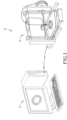
FIG. 1 is a perspective view of a computer modeling and additive manufacturing system constructed in accordance with an embodiment of the present invention; -
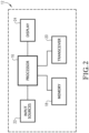
FIG. 2 is a schematic view of the computer modeling system ofFIG. 1 ; -
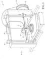
FIG. 3 is a perspective view of the additive manufacturing system ofFIG. 1 ; -
FIG. 4 is a perspective view of an overall shape of a part modeled via the computer modeling system ofFIG. 1 ; -
FIG. 5 is an elevational cutaway view of the overall shape ofFIG. 4 ; -
FIG. 6 is a finite element mesh of the overall shape of the part ofFIG. 4 ; -
FIG. 7 is an elevational cutaway view of the finite element mesh ofFIG. 6 ; -
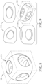
FIG. 8 is a perspective view of a lattice cellular component within a mesh element; -
FIG. 9 is a perspective view of the lattice cellular component ofFIG. 8 being deformed; -
FIG. 10 is a top view of the part having a lattice structure based on the lattice cellular component ofFIG. 8 ; -
FIG. 11 is an elevational partial cutaway view of the lattice structure ofFIG. 10 ; -
FIG. 12 is a flow diagram of a method of creating a part design via the computer modeling system ofFIG. 2 ; and -
FIG. 13 is a flow diagram of a method of forming the part ofFIG. 10 via the additive manufacturing system ofFIG. 3 . - The drawings are not necessarily to scale, emphasis instead being placed upon clearly illustrating the principles of the invention.
- Turning to the drawing figures, and particularly
FIGS. 1-3 , a computer modeling andadditive manufacturing system 10 constructed in accordance with an embodiment of the present invention is illustrated. The computer modeling andadditive manufacturing system 10 broadly comprises a computer aided design (CAD)system 12 and anadditive manufacturing system 14. - The
CAD system 12 may be used for designing and generating a computer model of apart 100 and broadly includes a processor 16, a memory 18, a transceiver 20, a plurality of inputs 22, and a display 24. TheCAD system 12 may be integral with or separate from theadditive manufacturing system 14. - The processor 16 generates the computer model of the
part 100 according to inputs and data received from a user. The processor 16 may include a circuit board, memory, display, inputs, and/or other electronic components such as a transceiver or external connection for communicating with external computers and the like. - The processor 16 may implement aspects of the present invention with one or more computer programs stored in or on computer-readable medium residing on or accessible by the processor. Each computer program preferably comprises an ordered listing of executable instructions for implementing logical functions in the processor 16. Each computer program can be embodied in any non-transitory computer-readable medium, such as the memory 18 (described below), for use by or in connection with an instruction execution system, apparatus, or device, such as a computer-based system, processor-containing system, or other system that can fetch the instructions from the instruction execution system, apparatus, or device, and execute the instructions.
- The memory 18 may be any computer-readable non-transitory medium that can store the program for use by or in connection with the instruction execution system, apparatus, or device. The computer-readable medium can be, for example, but not limited to, an electronic, magnetic, optical, electro-magnetic, infrared, or semi-conductor system, apparatus, or device. More specific, although not inclusive, examples of the computer-readable medium would include the following: an electrical connection having one or more wires, a portable computer diskette, a random access memory (RAM), a read-only memory (ROM), an erasable, programmable, read-only memory (EPROM or Flash memory), an optical fiber, and a portable compact disk read-only memory (CDROM).
- The transceiver 20 may transmit data and instructions between the
CAD system 12 and theadditive manufacturing system 14 over a wireless communication network. Alternatively, a wired or integrated setup may be used between theCAD system 12 and theadditive manufacturing system 14. - The inputs 22 allow a user to design and modify a model of the
part 100 and may comprise a keyboard, mouse, trackball, touchscreen, buttons, dials, virtual inputs, and/or a virtual reality simulator. The inputs 22 may also be used to control or instruct theadditive manufacturing system 14. - The display 24 may display a two-dimensional or three-dimensional representation of the model and may also display model data, computer options, and other information via a graphical user interface (GUI). The display 24 may be separate from or integrated with the
additive manufacturing system 14. - The
additive manufacturing system 14 produces prototypes and parts such aspart 100 and broadly includes aframe 26, asupport surface 28, amaterial reserve 30, afeeder 32, amaterial applicator 34, a set ofmotors 36, and aprocessor 38. Theadditive manufacturing system 14 may be integral with or separate from thepowder coating system 14. - The
frame 26 provides structure for thesupport surface 28,material reserve 30,feeder 32,material applicator 34,motors 36, and/or theprocessor 38 and may include a base, vertical members, cross members, and mounting points for mounting the above components thereto. Alternatively, theframe 26 may be a walled housing or similar structure. - The
support surface 28 supports thepart 100 as it is being constructed and may be a stationary or movable flat tray or bed, a substrate, a mandrel, a wheel, scaffolding, or similar support. Thesupport surface 28 may be integral with theadditive manufacturing system 14 or may be removable and transferable with thepart 100 as thepart 100 is being constructed. - The
material reserve 30 retainsadditive manufacturing material 40 and may be a hopper, tank, cartridge, container, spool, or other similar material holder. The material reserve may be integral with theadditive manufacturing system 14 or may be disposable and/or reusable. - The
additive manufacturing material 40 may be used for formingpart 100 and may be in pellet or powder form, filament or spooled form, or any other suitable form. Theadditive manufacturing material 40 may be any plastic, polymer, or organic material suitable for use in additive manufacturing. For example, theadditive manufacturing material 40 may be acrylonitrile butadiene styrene (ABS), polyamide, straw-based plastic, or other similar material. - The
feeder 32 directs theadditive manufacturing material 40 to thematerial applicator 34 and may be a spool feeder, a pump, an auger, or any other suitable feeder. Alternatively, theadditive manufacturing material 40 may be gravity fed to thematerial applicator 34. - The
material applicator 34 deposits theadditive manufacturing material 40 onto thesupport surface 28 and previously constructed layers. Thematerial applicator 34 may include a nozzle, guide, sprayer, or other similar component for channeling theadditive manufacturing material 40 and a laser, heater, or similar component for melting the additive manufacturing material and bonding (e.g., sintering) theadditive manufacturing material 40 onto a previously constructed layer. Thematerial applicator 34 may be sized according to the size of the pellets, powder, or filament being deposited. - The
motors 36 position thematerial applicator 34 over thesupport surface 28 and previously constructed layers and move thematerial applicator 34 as the additive manufacturing material is deposited onto thesupport surface 28 and the previously constructed layers. Themotors 36 may be oriented orthogonally to each other so that a first one of themotors 36 is configured to move thematerial applicator 34 in a lateral "x" direction, a second one of themotors 36 is configured to move thematerial applicator 34 in a longitudinal "y" direction, and a third one of themotors 36 is configured to move thematerial applicator 34 in an altitudinal "z" direction. Alternatively, themotors 36 may move the support surface 28 (and hence the part 100) while thematerial applicator 34 remains stationary. - The
processor 38 directs thematerial applicator 34 via themotors 36 and activates thematerial applicator 34 such that thematerial applicator 34 deposits theadditive manufacturing material 40 onto thesupport surface 28 and previously constructed layers according to a computer aided design of the part. Theprocessor 38 may include a circuit board, memory, display, inputs, and/or other electronic components such as a transceiver or external connection for communicating with the processor 16 of theCAD system 12 and other external computers. It will be understood that theprocessor 38 may be one and the same as processor 16 of theCAD system 12. - The
processor 38 may implement aspects of the present invention with one or more computer programs stored in or on computer-readable medium residing on or accessible by the processor. Each computer program preferably comprises an ordered listing of executable instructions for implementing logical functions in theprocessor 38. Each computer program can be embodied in any non-transitory computer-readable medium for use by or in connection with an instruction execution system, apparatus, or device, such as a computer-based system, processor-containing system, or other system that can fetch the instructions from the instruction execution system, apparatus, or device, and execute the instructions. In the context of this application, a "computer-readable medium" can be any non-transitory means that can store the program for use by or in connection with the instruction execution system, apparatus, or device. The computer-readable medium can be, for example, but not limited to, an electronic, magnetic, optical, electro-magnetic, infrared, or semi-conductor system, apparatus, or device. More specific, although not inclusive, examples of the computer-readable medium would include the following: an electrical connection having one or more wires, a portable computer diskette, a random access memory (RAM), a read-only memory (ROM), an erasable, programmable, read-only memory (EPROM or Flash memory), an optical fiber, and a portable compact disk read-only memory (CDROM). - It will be understood that the
additive manufacturing system 14 may be any type of additive manufacturing or "3D printing" system such as a sintering, laser melting, laser sintering, extruding, fusing, stereolithography, extrusion, light polymerizing, powder bed, wire additive, or laminated object manufacturing system. Theadditive manufacturing system 14 may also be a hybrid system that combines additive manufacturing with molding, scaffolding, and/or other subtractive manufacturing or assembly techniques. - Turning to
FIGS. 12 and 13 , and with reference toFIGS. 4-11 , use of the computer modeling andadditive manufacturing system 10 for creating a computer model of thepart 100 and forming thepart 100 via additive manufacturing according to the computer model will now be described in more detail. First, a computer-aided model may be created (or received from another computer system), in which anoverall shape 102 of the part 100 (FIG. 4 ) may be generated, as shown inblock 200 ofFIG. 12 . This may be a wire-frame model, surface model, solid model, or any other suitable CAD model that defines or exhibits theoverall shape 102 of thepart 100. - The
overall shape 102 of thepart 100 may optionally be divided into two ormore sections 104a,b (FIG. 5 ), as shown inblock 202. One or more of thesections 104a,b may encompass a portion of thepart 100 that will only be subjected to basic lattice deformations. For example,section 104b may include lattice cellular components that will be deformed only via basic lattice deformations such as translation, rotation, and/or isotropic, orthotropic, and anisotropic scaling to form the lower portion of the part. This may reduce or simplify calculations and rendering performed by theCAD system 12. - A finite element mesh 106 (shown fully deformed in
FIGS. 6 and 7 ) may then be created, as shown inblock 204. Thefinite element mesh 106 may include a plurality ofmesh elements 108 each representing a deformable unit. Eachmesh element 108 may have a number ofcorner nodes 110, a number ofedge midpoint nodes 112, face midpoint nodes, volume midpoint nodes, and/or any other nodes forming the basis ofmesh element 108 manipulation and deformation. For example, an 8-node hex will have corner nodes. A 20-node hex will have corner nodes and edge midpoint nodes. A 27-node hex will have corner nodes, edge midpoint nodes, face midpoint nodes, and a volume midpoint nodes. Thefinite element mesh 106 may be a first order, second order, or higher orderfinite element mesh 106 and may be triagonal, quadrilateral, tetrahedral, pyramidal, hexahedral, dodecahedral, or other polyhedral sub-volume shapes. Thefinite element mesh 106 thus includes sub-volumes (mesh elements 108) that provide spatial coordinates, as defined by the nodes for deformation processing. Higherorder mesh elements 108 can be used for higher order interpolation. Interpolation can be a free-form deformation, an isogeometric shape function, or an isoparametric shape function. Thefinite element mesh 106 may include mesh elements of two or more base shapes. Thefinite element mesh 106 may be created to conform to and be compliant with the overall shape of the part (FIGS. 6 and 7 ). However, thefinite element mesh 106 may undergo additional deformation, as described below. - The
finite element mesh 106 may optionally undergo smoothing, Jacobian optimization, Laplace optimization, regularity optimization, or other deformations, as shown inblock 206. Thefinite element mesh 106 may also be manually deformed or edited. - A lattice cellular component 114 (
FIGS. 8 and 9 ) may then be created, as shown inblock 208. The latticecellular component 114 may be a repeatable structural unit for populating the lattice structure (described below) and may itself be a wire-frame model, surface model, solid model, or any other suitable CAD model. The latticecellular component 114 may have a shape that coincides with the shape of themesh elements 108 of thefinite element mesh 106. For example, if thefinite element mesh 106 is quadrilateral, the latticecellular component 114 may also be quadrilateral and may extend to boundaries and/or nodes of anon-deformed mesh element 108. The latticecellular component 114 may include truss members, cross members, frame-like members, or any other structural components and may have chamfers, fillets, recesses, arches, and complex curves. The latticecellular component 114 may also include through-holes, channels, voids, chambers, and other negative spaces such that the resulting lattice structure is strong yet lightweight. This construction also simplifies and improves deformation of the lattice structure, as described below. The latticecellular component 114 may be honeycomb shaped, cube shaped, tube shaped, or any other suitable base shape. - A lattice structure 116 (shown fully deformed in
FIGS. 10 and 11 ) based on the latticecellular component 114 may then be generated, as shown inblock 210. Each component in thelattice structure 116 may correspond to amesh element 108 of thefinite element mesh 106. Thelattice structure 116 may be a matrix, array, or network of repetitions or copies of the latticecellular component 114. Thelattice structure 116 may include a honeycomb pattern, tube pattern, cube pattern, or any other pattern. The pattern may extend along one or more axes. In some embodiments, thelattice structure 116 may include lattice cellular components of two or more different base shapes. - The
lattice structure 116 may then be modified to conform to the deformedfinite element mesh 106 such that thelattice structure 116 has a cellular periodicity corresponding to themesh elements 108 of thefinite element mesh 106, as shown inblock 212. In this way, thelattice structure 116 conforms to theoverall shape 102 of thepart 100. In one embodiment, thelattice structure 116 may be sampled at various points along its surface or within its volume. The surface may be faceted, where each facet may be a polygon including vertices and edges. This faceted form may be stored as a stereolithography (STL) file, Polygon file (PLY) file, Additive Manufacturing file (AMF), or as a finite element mesh. The vertices then provide spatial coordinates for evaluating thedeformed mesh elements 108 or latticecellular components 114. Deformation of each latticecellular component 114 may include rotation and translation, in addition to stretching and skewing. That is, a lattice cellular component may undergo global deformation without undergoing local deformation. Note that thepart 100 may essentially be theabove lattice structure 116 or may include a shell, housing, outer wall, mounting bosses, and other major features in addition to thelattice structure 116. - Turning to
FIG. 13 , and with reference toFIG. 3 , thepart 100 may then be created via theadditive manufacturing system 14. First, the additive manufacturing material may be inserted in or positioned on thematerial reserve 30 of theadditive manufacturing system 14, as shown inblock 300. For example, a spool of theadditive manufacturing material 40 may be loaded onto theadditive manufacturing system 14. - The
additive manufacturing material 40 may then be deposited onto thesupport surface 28 via thematerial applicator 34 in successive layers according to the computer-aided design of thepart 100, as shown inblock 302. To that end, activation of horizontally oriented motors in various amounts allows for diagonal movement and curved movement of thematerial applicator 34. Activation of a vertically oriented motor may be used for relocating thematerial applicator 34 without depositing material and/or raising thematerial applicator 34 for creation of a new layer (seemotors 36, above). - The above-described computer modeling and
additive manufacturing system 10 and method provide several advantages over conventional systems. For example, features of thelattice structure 116 are not cut or compromised to form theoverall shape 102 of thepart 100. This eliminates structural weak points, stress concentrations, and inefficient or imperfect structural properties. For example, an axially symmetric part would be expected to have axially symmetric structural properties. However, if the axially symmetric part is formed of an orthogonal lattice structure, stress concentrations will form where the orthogonal lattice structure is truncated to form the overall shape of the axially symmetric part. The computer modeling andadditive manufacturing system 10 eliminates this problem. The arrangement, size, and shape distribution of the latticecellular components 114 may also be modified. Eachmesh element 108 of thefinite element mesh 106 may be recognized as avalid mesh element 108 by the software. As such, the physical properties of each modified latticecellular component 114 can be used to apply a reduced-order model to theparent mesh elements 108 of the modified latticecellular components 114 so as to reduce the computational complexity of a subsequent simulation. TheCAD system 12 may also be used for analyzing and iteratively improving and optimizing thelattice structure 116.
Claims (15)
- A method of creating a lattice structure for a part (100) formed via additive manufacturing, the method comprising the steps of:- receiving a computer model of the part (100) via a processor (16) of a computer modeling system (12), the computer model having an overall shape;- storing the computer model in a non-transitory computer-readable memory (18) of the computer modeling system (12);- generating a finite element mesh (106) corresponding to the overall shape of the part (100) via the processor (16), the finite element mesh (106) having a plurality of mesh elements (108);- storing the finite element mesh (106) in the non-transitory computer-readable memory (18);- generating a lattice cellular component (114) via the processor (16), the lattice cellular component (114) corresponding to a mesh element (108) of the finite element mesh (106);- storing the lattice cellular component (114) in the non-transitory computer-readable memory (18);- generating a lattice structure (116) based on the lattice cellular component (114) via the processor (16); and- storing the lattice structure (116) in the non-transitory computer-readable memory (18);- deforming the lattice structure (116) such that the lattice structure (116) has a cellular periodicity corresponding to the mesh elements (108) of the finite element mesh (106) so that the lattice structure (116) conforms to the shape of the part (100).
- The method of claim 1, further comprising the step of deforming at least some of the mesh elements (108) of the finite element mesh (106).
- The method of claim 1, wherein each finite element of the finite element mesh (106) includes a plurality of nodes (110, 112), the step of conforming the lattice structure (116) to the shape of the part (100) further including shifting at least some nodes of the plurality of nodes.
- The method of claim 1, wherein periodicity of each cell with neighboring cells is maintained when conforming the lattice structure (116) to the shape of the part (100).
- The method of claim 1, wherein the part (100) has axial symmetry and the lattice structure (116) conforms to the axial symmetry of the part.
- The method of claim 1, wherein the step of conforming the lattice structure (116) to the shape of the part (100) includes free-form deforming a plurality of the mesh elements of the finite element mesh (106).
- The method of claim 1, wherein the finite element mesh (106) is a first order finite element mesh, and/or
wherein the finite element mesh (106) is a greater-than-first-order finite element mesh. - The method of claim 1, wherein the finite element mesh (106) is a hexahedral finite element mesh, and/orwherein the finite element mesh (106) is a tetrahedral finite element mesh, and/orwherein the finite element mesh (106) is a pyramidal finite element mesh.
- The method of claim 1, wherein the finite element mesh (106) includes mesh elements having at least two different base shapes.
- The method of claim 1, wherein the lattice structure (116) includes honeycomb-shaped cells, and/orwherein the lattice structure (116) includes tube shaped cells, and/orwherein the lattice structure (116) includes cells of at least two different base shapes.
- The method of claim 1, wherein the lattice structure (116) is configured to be formed via additive manufacturing.
- A system (10) for creating a part (100) via additive manufacturing, the system comprising:- a computer modeling system (12) comprising:- a processor (16) configured to:- receive a computer model of the part (100) according to inputs received from a user, the computer model having an overall shape;- generate a finite element mesh (106) corresponding to the overall shape of the part (100), the finite element mesh (106) having a plurality of mesh elements (108);- generate a lattice cellular component (114) according to inputs received from the user, the lattice cellular component (114) corresponding to a mesh element (108) of the finite element mesh (106); and- generate a lattice structure (116) based on the lattice cellular component (114); and- deform the lattice structure (116), such that the lattice structure (116) has a cellular periodicity corresponding to the mesh elements of the finite element mesh (106) so that the lattice structure (116) conforms to the shape of the part (100);- a non-transitory computer-readable memory (18) configured to store the computer model, finite element mesh (106), lattice cellular component (114), and lattice structure (116) thereon;- a transceiver (20) for communicating with other devices over a wireless communication network;- a plurality of inputs (22) for receiving the inputs of the user; and- a display (24) configured to visually produce the computer model, finite element mesh (106), lattice cellular component (114), and lattice structure (116) to aid the user in developing the part; and- an additive manufacturing system (14) configured to produce the lattice structure (116) via additive manufacturing material deposited layer by layer according to the computer model of the part (20).
- The system of claim 12, wherein the processor is further configured to deform at least some of the mesh elements (108) of the finite element mesh (106).
- The system of claim 12, wherein the lattice structure (116) is formed of at least two different base shapes.
- The method of claim 1, the method comprising the steps of:- dividing the computer model of the part into at least two sections;- generating a hexahedron finite element mesh corresponding to the at least two sections of the computer model of the part, the finite element mesh having a plurality of mesh elements each having a plurality of corner nodes and edge midpoint nodes; and- shifting corner nodes and edge midpoint nodes of at least some of the mesh elements of the finite element mesh in one of the two sections such that the finite element mesh conforms to the overall shape of the part.
Applications Claiming Priority (2)
| Application Number | Priority Date | Filing Date | Title |
|---|---|---|---|
| US14/997,238 US10274935B2 (en) | 2016-01-15 | 2016-01-15 | System, method, and computer program for creating geometry-compliant lattice structures |
| PCT/US2016/023953 WO2017123268A1 (en) | 2016-01-15 | 2016-03-24 | System, method, and computer program for creating geometry-compliant lattice structures |
Publications (3)
| Publication Number | Publication Date |
|---|---|
| EP3402649A1 EP3402649A1 (en) | 2018-11-21 |
| EP3402649A4 EP3402649A4 (en) | 2019-10-30 |
| EP3402649B1 true EP3402649B1 (en) | 2024-07-24 |
Family
ID=59311356
Family Applications (1)
| Application Number | Title | Priority Date | Filing Date |
|---|---|---|---|
| EP16885367.9A Active EP3402649B1 (en) | 2016-01-15 | 2016-03-24 | System, method, and computer program for creating geometry-compliant lattice structures |
Country Status (3)
| Country | Link |
|---|---|
| US (4) | US10274935B2 (en) |
| EP (1) | EP3402649B1 (en) |
| WO (1) | WO2017123268A1 (en) |
Families Citing this family (19)
| Publication number | Priority date | Publication date | Assignee | Title |
|---|---|---|---|---|
| US10274935B2 (en) * | 2016-01-15 | 2019-04-30 | Honeywell Federal Manufacturing & Technologies, Llc | System, method, and computer program for creating geometry-compliant lattice structures |
| DE102016224023A1 (en) * | 2016-12-02 | 2018-06-07 | Ford Global Technologies, Llc | Control arm for a wheel suspension of a vehicle and method for its production |
| US11086294B2 (en) * | 2017-04-12 | 2021-08-10 | Autodesk, Inc. | Combining additive and conventional manufacturing techniques to improve manufacturability |
| US10875244B2 (en) * | 2017-05-17 | 2020-12-29 | Slice Engineering LLC | Adaptable high-performance extrusion head for fused filament fabrication systems |
| US10073440B1 (en) * | 2018-02-13 | 2018-09-11 | University Of Central Florida Research Foundation, Inc. | Method for the design and manufacture of composites having tunable physical properties |
| EP3820700B1 (en) * | 2018-10-22 | 2025-08-20 | Carbon, Inc. | Lattice transitioning structures in additively manufactured products |
| AU2019445440A1 (en) * | 2019-05-16 | 2021-12-02 | Spherene Ag | Method for the lightweighting and/or designing of an additively manufactured article |
| WO2021055803A1 (en) * | 2019-09-18 | 2021-03-25 | Autodesk, Inc. | Hybrid additive and subtractive manufacturing |
| US12391000B2 (en) | 2019-10-17 | 2025-08-19 | Honeywell Federal Manufacturing & Technologies, Llc | System and method for creating lattice structures |
| DE102019135526A1 (en) | 2019-11-19 | 2021-05-20 | Ktm E-Technologies Gmbh | Method for creating a virtual three-dimensional structure model |
| US11727162B2 (en) * | 2019-11-25 | 2023-08-15 | Akselos S.A. | Methods and systems for component-based reduced order modeling for industrial-scale structural digital twins |
| US12326717B2 (en) | 2019-11-25 | 2025-06-10 | Akselos S.A. | Methods and systems for component-based reduced order modeling for industrial-scale structural digital twins |
| US11514210B2 (en) * | 2019-12-10 | 2022-11-29 | Lawrence Livermore National Security, Llc | Component-wise reduced-order model design optimization such as for lattice design optimization |
| US12049043B2 (en) | 2020-03-24 | 2024-07-30 | Proto Labs, Inc. | Methods and systems for generating a three-dimensional product having a cubic internal structure |
| CN112560125B (en) * | 2020-12-10 | 2023-03-24 | 上海联泰科技股份有限公司 | Generation method, generation system and preprocessing system of lattice structure model |
| USD980882S1 (en) * | 2020-12-31 | 2023-03-14 | Slice Engineering, Llc | 3D printer hotend |
| CN115048830B (en) * | 2022-05-17 | 2024-12-24 | 华中科技大学 | A method for simulating additive manufacturing partitioning process |
| KR102667895B1 (en) * | 2023-03-08 | 2024-05-23 | 서울과학기술대학교 산학협력단 | Data generation device and data generation method for 3D printing of micro-lattice structures |
| CN120912692B (en) * | 2025-09-29 | 2026-01-20 | 山东华云三维科技有限公司 | Lattice data compression method, system and medium for additive manufacturing |
Family Cites Families (24)
| Publication number | Priority date | Publication date | Assignee | Title |
|---|---|---|---|---|
| US5946479A (en) * | 1995-05-25 | 1999-08-31 | Matsushita Electric Industrial Co., Ltd. | Method and device for generating mesh for use in numerical analysis |
| US6788865B2 (en) * | 2000-03-03 | 2004-09-07 | Nippon Telegraph And Telephone Corporation | Polarization maintaining optical fiber with improved polarization maintaining property |
| WO2002043006A1 (en) | 2000-11-27 | 2002-05-30 | Ding Huang | Modeling object interactions and facial expressions |
| US7324103B2 (en) * | 2001-10-30 | 2008-01-29 | Ford Motor Company | System and method of direct mesh manipulation |
| US6936212B1 (en) | 2002-02-07 | 2005-08-30 | 3D Systems, Inc. | Selective deposition modeling build style providing enhanced dimensional accuracy |
| US7275023B2 (en) * | 2003-01-29 | 2007-09-25 | Ford Motor Company | System and method of interactively generating a family of mesh models |
| US20060119578A1 (en) | 2004-11-11 | 2006-06-08 | Thenkurussi Kesavadas | System for interfacing between an operator and a virtual object for computer aided design applications |
| US7286127B2 (en) | 2005-06-22 | 2007-10-23 | Microsoft Corporation | Large mesh deformation using the volumetric graph Laplacian |
| US7843467B2 (en) | 2006-12-18 | 2010-11-30 | Microsoft Corporation | Shape deformation |
| US20080275677A1 (en) | 2007-03-19 | 2008-11-06 | Optimal Solutions Software, Llc | System, methods, and computer readable media, for product design using coupled computer aided engineering models |
| US20110107904A1 (en) * | 2007-08-15 | 2011-05-12 | University Of Virginia Patent Foundation | Synergistically-Layered Armor Systems and Methods for Producing Layers Thereof |
| JP2009166422A (en) | 2008-01-18 | 2009-07-30 | Hitachi Kokusai Electric Inc | Formation method of stereolithography |
| US8828311B2 (en) | 2009-05-15 | 2014-09-09 | Board Of Regents, The University Of Texas System | Reticulated mesh arrays and dissimilar array monoliths by additive layered manufacturing using electron and laser beam melting |
| US8831913B2 (en) | 2009-06-10 | 2014-09-09 | Airbus Operations Limited | Method of design optimisation |
| GB201003065D0 (en) | 2010-02-23 | 2010-04-07 | Simpleware Ltd | Image processing method and method of three-dimensional printing incorporating the same |
| WO2013192599A1 (en) | 2012-06-21 | 2013-12-27 | Massachusetts Institute Of Technology | Methods and apparatus for digital material skins |
| US9042613B2 (en) * | 2013-03-01 | 2015-05-26 | Heartflow, Inc. | Method and system for determining treatments by modifying patient-specific geometrical models |
| US9348948B2 (en) * | 2013-03-14 | 2016-05-24 | Spirit Aerosystems, Inc. | Method of part verification |
| US10696009B2 (en) | 2014-01-07 | 2020-06-30 | Nama Development Llc | 3-D honeycomb foam structure |
| US9902114B2 (en) | 2014-01-09 | 2018-02-27 | Siemens Product Lifecycle Management Software Inc. | Method for creating three dimensional lattice structures in computer-aided design models for additive manufacturing |
| US9102099B1 (en) * | 2014-02-05 | 2015-08-11 | MetaMason, Inc. | Methods for additive manufacturing processes incorporating active deposition |
| JP6289142B2 (en) * | 2014-02-07 | 2018-03-07 | キヤノン株式会社 | Image processing apparatus, image processing method, program, and storage medium |
| US10062202B2 (en) * | 2014-12-22 | 2018-08-28 | General Electric Company | System and methods of generating a computer model of a composite component |
| US10274935B2 (en) | 2016-01-15 | 2019-04-30 | Honeywell Federal Manufacturing & Technologies, Llc | System, method, and computer program for creating geometry-compliant lattice structures |
-
2016
- 2016-01-15 US US14/997,238 patent/US10274935B2/en active Active
- 2016-03-24 EP EP16885367.9A patent/EP3402649B1/en active Active
- 2016-03-24 WO PCT/US2016/023953 patent/WO2017123268A1/en not_active Ceased
-
2019
- 2019-03-27 US US16/366,690 patent/US10642253B2/en active Active
-
2020
- 2020-05-04 US US16/865,729 patent/US11073819B2/en active Active
-
2021
- 2021-07-06 US US17/367,936 patent/US11989003B2/en active Active
Also Published As
| Publication number | Publication date |
|---|---|
| US10274935B2 (en) | 2019-04-30 |
| US20210341903A1 (en) | 2021-11-04 |
| EP3402649A4 (en) | 2019-10-30 |
| US10642253B2 (en) | 2020-05-05 |
| US20170203516A1 (en) | 2017-07-20 |
| US20190219986A1 (en) | 2019-07-18 |
| WO2017123268A1 (en) | 2017-07-20 |
| EP3402649A1 (en) | 2018-11-21 |
| US20200264586A1 (en) | 2020-08-20 |
| US11073819B2 (en) | 2021-07-27 |
| US11989003B2 (en) | 2024-05-21 |
Similar Documents
| Publication | Publication Date | Title |
|---|---|---|
| EP3402649B1 (en) | System, method, and computer program for creating geometry-compliant lattice structures | |
| US11307560B2 (en) | System, method and computer program for creating united cellular lattice structure | |
| US12427721B2 (en) | System, method, and computer program for creating an internal conforming structure | |
| US12233603B2 (en) | Slicer systems for generating a molecular dynamic graded lattice structure and their application to additive manufacturing | |
| US9434109B2 (en) | Three-dimensional printing method | |
| US10802467B2 (en) | Methods of defining internal structures for additive manufacturing | |
| EP3877890A1 (en) | Macrostructure topology generation with physical simulation for computer aided design and manufacturing | |
| IL288076A (en) | Method for the lightweighting and/or designing of an additively manufactured article | |
| US20190325098A1 (en) | System, method, and computer program for part model generation and analysis and part production and validation | |
| EP3545443A1 (en) | Adaptive topology optimization for additive layer manufacturing | |
| JP2023527287A (en) | 2. Computer Aided Generative Design with Layer Boundary Determination to Facilitate 5-Axis Rejection Manufacturing Process | |
| Zhong et al. | Ceramic 3D printed sweeping surfaces | |
| JP2020524093A (en) | Method, device, and system for parts-to-build | |
| EP3122540B1 (en) | Method and equipment for generating a numerical representation of a three-dimensional object, said numerical representation being suited to be used for making said three-dimensional object through stereolithography | |
| US12391000B2 (en) | System and method for creating lattice structures | |
| KR101631474B1 (en) | Three dimensional model creating method for digital manufacture | |
| JP7813213B2 (en) | Computer-aided design with geometry filtering to expedite manufacturing | |
| Li et al. | Virtual-Trim: A parametric geometric modeling method for heterogeneous strut-based lattice structures | |
| CN121435777A (en) | Method, apparatus, equipment and storage medium for smoothing feed surface based on curve fitting | |
| CN115935530A (en) | 3D Surface Pattern Generation for Part Creation in Computer Aided Design and Manufacturing | |
| CHOO et al. | COMPUTATIONAL DESIGN FOR ADDITIVE MANUFACTURING OF A DOUBLY CURVED GYROID LATTICE WALL |
Legal Events
| Date | Code | Title | Description |
|---|---|---|---|
| STAA | Information on the status of an ep patent application or granted ep patent |
Free format text: STATUS: THE INTERNATIONAL PUBLICATION HAS BEEN MADE |
|
| PUAI | Public reference made under article 153(3) epc to a published international application that has entered the european phase |
Free format text: ORIGINAL CODE: 0009012 |
|
| STAA | Information on the status of an ep patent application or granted ep patent |
Free format text: STATUS: REQUEST FOR EXAMINATION WAS MADE |
|
| 17P | Request for examination filed |
Effective date: 20180406 |
|
| AK | Designated contracting states |
Kind code of ref document: A1 Designated state(s): AL AT BE BG CH CY CZ DE DK EE ES FI FR GB GR HR HU IE IS IT LI LT LU LV MC MK MT NL NO PL PT RO RS SE SI SK SM TR |
|
| AX | Request for extension of the european patent |
Extension state: BA ME |
|
| DAV | Request for validation of the european patent (deleted) | ||
| DAX | Request for extension of the european patent (deleted) | ||
| A4 | Supplementary search report drawn up and despatched |
Effective date: 20191001 |
|
| RIC1 | Information provided on ipc code assigned before grant |
Ipc: B33Y 70/00 20150101ALI20190925BHEP Ipc: B29C 67/00 20170101AFI20190925BHEP Ipc: G06F 17/50 20060101ALI20190925BHEP Ipc: B33Y 50/00 20150101ALI20190925BHEP Ipc: B33Y 10/00 20150101ALI20190925BHEP |
|
| STAA | Information on the status of an ep patent application or granted ep patent |
Free format text: STATUS: EXAMINATION IS IN PROGRESS |
|
| 17Q | First examination report despatched |
Effective date: 20220204 |
|
| GRAP | Despatch of communication of intention to grant a patent |
Free format text: ORIGINAL CODE: EPIDOSNIGR1 |
|
| STAA | Information on the status of an ep patent application or granted ep patent |
Free format text: STATUS: GRANT OF PATENT IS INTENDED |
|
| RIC1 | Information provided on ipc code assigned before grant |
Ipc: B33Y 70/00 20150101ALI20240205BHEP Ipc: B33Y 50/00 20150101ALI20240205BHEP Ipc: B33Y 10/00 20150101ALI20240205BHEP Ipc: B29C 67/00 20170101AFI20240205BHEP |
|
| INTG | Intention to grant announced |
Effective date: 20240227 |
|
| GRAS | Grant fee paid |
Free format text: ORIGINAL CODE: EPIDOSNIGR3 |
|
| GRAA | (expected) grant |
Free format text: ORIGINAL CODE: 0009210 |
|
| STAA | Information on the status of an ep patent application or granted ep patent |
Free format text: STATUS: THE PATENT HAS BEEN GRANTED |
|
| AK | Designated contracting states |
Kind code of ref document: B1 Designated state(s): AL AT BE BG CH CY CZ DE DK EE ES FI FR GB GR HR HU IE IS IT LI LT LU LV MC MK MT NL NO PL PT RO RS SE SI SK SM TR |
|
| REG | Reference to a national code |
Ref country code: GB Ref legal event code: FG4D |
|
| REG | Reference to a national code |
Ref country code: CH Ref legal event code: EP |
|
| REG | Reference to a national code |
Ref country code: IE Ref legal event code: FG4D Ref country code: DE Ref legal event code: R096 Ref document number: 602016088587 Country of ref document: DE |
|
| REG | Reference to a national code |
Ref country code: LT Ref legal event code: MG9D |
|
| REG | Reference to a national code |
Ref country code: NL Ref legal event code: MP Effective date: 20240724 |
|
| PG25 | Lapsed in a contracting state [announced via postgrant information from national office to epo] |
Ref country code: PT Free format text: LAPSE BECAUSE OF FAILURE TO SUBMIT A TRANSLATION OF THE DESCRIPTION OR TO PAY THE FEE WITHIN THE PRESCRIBED TIME-LIMIT Effective date: 20241125 |
|
| REG | Reference to a national code |
Ref country code: AT Ref legal event code: MK05 Ref document number: 1705950 Country of ref document: AT Kind code of ref document: T Effective date: 20240724 |
|
| PG25 | Lapsed in a contracting state [announced via postgrant information from national office to epo] |
Ref country code: NL Free format text: LAPSE BECAUSE OF FAILURE TO SUBMIT A TRANSLATION OF THE DESCRIPTION OR TO PAY THE FEE WITHIN THE PRESCRIBED TIME-LIMIT Effective date: 20240724 |
|
| PG25 | Lapsed in a contracting state [announced via postgrant information from national office to epo] |
Ref country code: PT Free format text: LAPSE BECAUSE OF FAILURE TO SUBMIT A TRANSLATION OF THE DESCRIPTION OR TO PAY THE FEE WITHIN THE PRESCRIBED TIME-LIMIT Effective date: 20241125 Ref country code: NL Free format text: LAPSE BECAUSE OF FAILURE TO SUBMIT A TRANSLATION OF THE DESCRIPTION OR TO PAY THE FEE WITHIN THE PRESCRIBED TIME-LIMIT Effective date: 20240724 |
|
| PG25 | Lapsed in a contracting state [announced via postgrant information from national office to epo] |
Ref country code: NO Free format text: LAPSE BECAUSE OF FAILURE TO SUBMIT A TRANSLATION OF THE DESCRIPTION OR TO PAY THE FEE WITHIN THE PRESCRIBED TIME-LIMIT Effective date: 20241024 |
|
| PG25 | Lapsed in a contracting state [announced via postgrant information from national office to epo] |
Ref country code: FI Free format text: LAPSE BECAUSE OF FAILURE TO SUBMIT A TRANSLATION OF THE DESCRIPTION OR TO PAY THE FEE WITHIN THE PRESCRIBED TIME-LIMIT Effective date: 20240724 Ref country code: GR Free format text: LAPSE BECAUSE OF FAILURE TO SUBMIT A TRANSLATION OF THE DESCRIPTION OR TO PAY THE FEE WITHIN THE PRESCRIBED TIME-LIMIT Effective date: 20241025 Ref country code: PL Free format text: LAPSE BECAUSE OF FAILURE TO SUBMIT A TRANSLATION OF THE DESCRIPTION OR TO PAY THE FEE WITHIN THE PRESCRIBED TIME-LIMIT Effective date: 20240724 |
|
| PG25 | Lapsed in a contracting state [announced via postgrant information from national office to epo] |
Ref country code: BG Free format text: LAPSE BECAUSE OF FAILURE TO SUBMIT A TRANSLATION OF THE DESCRIPTION OR TO PAY THE FEE WITHIN THE PRESCRIBED TIME-LIMIT Effective date: 20240724 |
|
| PG25 | Lapsed in a contracting state [announced via postgrant information from national office to epo] |
Ref country code: LV Free format text: LAPSE BECAUSE OF FAILURE TO SUBMIT A TRANSLATION OF THE DESCRIPTION OR TO PAY THE FEE WITHIN THE PRESCRIBED TIME-LIMIT Effective date: 20240724 |
|
| PG25 | Lapsed in a contracting state [announced via postgrant information from national office to epo] |
Ref country code: AT Free format text: LAPSE BECAUSE OF FAILURE TO SUBMIT A TRANSLATION OF THE DESCRIPTION OR TO PAY THE FEE WITHIN THE PRESCRIBED TIME-LIMIT Effective date: 20240724 Ref country code: IS Free format text: LAPSE BECAUSE OF FAILURE TO SUBMIT A TRANSLATION OF THE DESCRIPTION OR TO PAY THE FEE WITHIN THE PRESCRIBED TIME-LIMIT Effective date: 20241124 |
|
| PG25 | Lapsed in a contracting state [announced via postgrant information from national office to epo] |
Ref country code: HR Free format text: LAPSE BECAUSE OF FAILURE TO SUBMIT A TRANSLATION OF THE DESCRIPTION OR TO PAY THE FEE WITHIN THE PRESCRIBED TIME-LIMIT Effective date: 20240724 |
|
| PG25 | Lapsed in a contracting state [announced via postgrant information from national office to epo] |
Ref country code: ES Free format text: LAPSE BECAUSE OF FAILURE TO SUBMIT A TRANSLATION OF THE DESCRIPTION OR TO PAY THE FEE WITHIN THE PRESCRIBED TIME-LIMIT Effective date: 20240724 Ref country code: RS Free format text: LAPSE BECAUSE OF FAILURE TO SUBMIT A TRANSLATION OF THE DESCRIPTION OR TO PAY THE FEE WITHIN THE PRESCRIBED TIME-LIMIT Effective date: 20241024 |
|
| PG25 | Lapsed in a contracting state [announced via postgrant information from national office to epo] |
Ref country code: RS Free format text: LAPSE BECAUSE OF FAILURE TO SUBMIT A TRANSLATION OF THE DESCRIPTION OR TO PAY THE FEE WITHIN THE PRESCRIBED TIME-LIMIT Effective date: 20241024 Ref country code: PL Free format text: LAPSE BECAUSE OF FAILURE TO SUBMIT A TRANSLATION OF THE DESCRIPTION OR TO PAY THE FEE WITHIN THE PRESCRIBED TIME-LIMIT Effective date: 20240724 Ref country code: NO Free format text: LAPSE BECAUSE OF FAILURE TO SUBMIT A TRANSLATION OF THE DESCRIPTION OR TO PAY THE FEE WITHIN THE PRESCRIBED TIME-LIMIT Effective date: 20241024 Ref country code: LV Free format text: LAPSE BECAUSE OF FAILURE TO SUBMIT A TRANSLATION OF THE DESCRIPTION OR TO PAY THE FEE WITHIN THE PRESCRIBED TIME-LIMIT Effective date: 20240724 Ref country code: IS Free format text: LAPSE BECAUSE OF FAILURE TO SUBMIT A TRANSLATION OF THE DESCRIPTION OR TO PAY THE FEE WITHIN THE PRESCRIBED TIME-LIMIT Effective date: 20241124 Ref country code: HR Free format text: LAPSE BECAUSE OF FAILURE TO SUBMIT A TRANSLATION OF THE DESCRIPTION OR TO PAY THE FEE WITHIN THE PRESCRIBED TIME-LIMIT Effective date: 20240724 Ref country code: GR Free format text: LAPSE BECAUSE OF FAILURE TO SUBMIT A TRANSLATION OF THE DESCRIPTION OR TO PAY THE FEE WITHIN THE PRESCRIBED TIME-LIMIT Effective date: 20241025 Ref country code: FI Free format text: LAPSE BECAUSE OF FAILURE TO SUBMIT A TRANSLATION OF THE DESCRIPTION OR TO PAY THE FEE WITHIN THE PRESCRIBED TIME-LIMIT Effective date: 20240724 Ref country code: ES Free format text: LAPSE BECAUSE OF FAILURE TO SUBMIT A TRANSLATION OF THE DESCRIPTION OR TO PAY THE FEE WITHIN THE PRESCRIBED TIME-LIMIT Effective date: 20240724 Ref country code: BG Free format text: LAPSE BECAUSE OF FAILURE TO SUBMIT A TRANSLATION OF THE DESCRIPTION OR TO PAY THE FEE WITHIN THE PRESCRIBED TIME-LIMIT Effective date: 20240724 Ref country code: AT Free format text: LAPSE BECAUSE OF FAILURE TO SUBMIT A TRANSLATION OF THE DESCRIPTION OR TO PAY THE FEE WITHIN THE PRESCRIBED TIME-LIMIT Effective date: 20240724 |
|
| PG25 | Lapsed in a contracting state [announced via postgrant information from national office to epo] |
Ref country code: DK Free format text: LAPSE BECAUSE OF FAILURE TO SUBMIT A TRANSLATION OF THE DESCRIPTION OR TO PAY THE FEE WITHIN THE PRESCRIBED TIME-LIMIT Effective date: 20240724 Ref country code: SM Free format text: LAPSE BECAUSE OF FAILURE TO SUBMIT A TRANSLATION OF THE DESCRIPTION OR TO PAY THE FEE WITHIN THE PRESCRIBED TIME-LIMIT Effective date: 20240724 Ref country code: RO Free format text: LAPSE BECAUSE OF FAILURE TO SUBMIT A TRANSLATION OF THE DESCRIPTION OR TO PAY THE FEE WITHIN THE PRESCRIBED TIME-LIMIT Effective date: 20240724 |
|
| PG25 | Lapsed in a contracting state [announced via postgrant information from national office to epo] |
Ref country code: EE Free format text: LAPSE BECAUSE OF FAILURE TO SUBMIT A TRANSLATION OF THE DESCRIPTION OR TO PAY THE FEE WITHIN THE PRESCRIBED TIME-LIMIT Effective date: 20240724 |
|
| PG25 | Lapsed in a contracting state [announced via postgrant information from national office to epo] |
Ref country code: CZ Free format text: LAPSE BECAUSE OF FAILURE TO SUBMIT A TRANSLATION OF THE DESCRIPTION OR TO PAY THE FEE WITHIN THE PRESCRIBED TIME-LIMIT Effective date: 20240724 |
|
| REG | Reference to a national code |
Ref country code: DE Ref legal event code: R097 Ref document number: 602016088587 Country of ref document: DE |
|
| PG25 | Lapsed in a contracting state [announced via postgrant information from national office to epo] |
Ref country code: IT Free format text: LAPSE BECAUSE OF FAILURE TO SUBMIT A TRANSLATION OF THE DESCRIPTION OR TO PAY THE FEE WITHIN THE PRESCRIBED TIME-LIMIT Effective date: 20240724 Ref country code: SK Free format text: LAPSE BECAUSE OF FAILURE TO SUBMIT A TRANSLATION OF THE DESCRIPTION OR TO PAY THE FEE WITHIN THE PRESCRIBED TIME-LIMIT Effective date: 20240724 |
|
| PLBE | No opposition filed within time limit |
Free format text: ORIGINAL CODE: 0009261 |
|
| STAA | Information on the status of an ep patent application or granted ep patent |
Free format text: STATUS: NO OPPOSITION FILED WITHIN TIME LIMIT |
|
| 26N | No opposition filed |
Effective date: 20250425 |
|
| PG25 | Lapsed in a contracting state [announced via postgrant information from national office to epo] |
Ref country code: SE Free format text: LAPSE BECAUSE OF FAILURE TO SUBMIT A TRANSLATION OF THE DESCRIPTION OR TO PAY THE FEE WITHIN THE PRESCRIBED TIME-LIMIT Effective date: 20240724 |
|
| REG | Reference to a national code |
Ref country code: DE Ref legal event code: R119 Ref document number: 602016088587 Country of ref document: DE |
|
| PG25 | Lapsed in a contracting state [announced via postgrant information from national office to epo] |
Ref country code: MC Free format text: LAPSE BECAUSE OF FAILURE TO SUBMIT A TRANSLATION OF THE DESCRIPTION OR TO PAY THE FEE WITHIN THE PRESCRIBED TIME-LIMIT Effective date: 20240724 |
|
| REG | Reference to a national code |
Ref country code: CH Ref legal event code: H13 Free format text: ST27 STATUS EVENT CODE: U-0-0-H10-H13 (AS PROVIDED BY THE NATIONAL OFFICE) Effective date: 20251024 |
|
| PG25 | Lapsed in a contracting state [announced via postgrant information from national office to epo] |
Ref country code: LU Free format text: LAPSE BECAUSE OF NON-PAYMENT OF DUE FEES Effective date: 20250324 |
|
| PG25 | Lapsed in a contracting state [announced via postgrant information from national office to epo] |
Ref country code: DE Free format text: LAPSE BECAUSE OF NON-PAYMENT OF DUE FEES Effective date: 20251001 |
|
| PG25 | Lapsed in a contracting state [announced via postgrant information from national office to epo] |
Ref country code: CH Free format text: LAPSE BECAUSE OF NON-PAYMENT OF DUE FEES Effective date: 20250331 |
|
| PG25 | Lapsed in a contracting state [announced via postgrant information from national office to epo] |
Ref country code: IE Free format text: LAPSE BECAUSE OF NON-PAYMENT OF DUE FEES Effective date: 20250324 |
|
| PGFP | Annual fee paid to national office [announced via postgrant information from national office to epo] |
Ref country code: GB Payment date: 20260327 Year of fee payment: 11 |
|
| PGFP | Annual fee paid to national office [announced via postgrant information from national office to epo] |
Ref country code: BE Payment date: 20260327 Year of fee payment: 11 |
|
| PGFP | Annual fee paid to national office [announced via postgrant information from national office to epo] |
Ref country code: FR Payment date: 20260325 Year of fee payment: 11 |