EP3402076A1 - I-v conversion module - Google Patents
I-v conversion module Download PDFInfo
- Publication number
- EP3402076A1 EP3402076A1 EP16922161.1A EP16922161A EP3402076A1 EP 3402076 A1 EP3402076 A1 EP 3402076A1 EP 16922161 A EP16922161 A EP 16922161A EP 3402076 A1 EP3402076 A1 EP 3402076A1
- Authority
- EP
- European Patent Office
- Prior art keywords
- integral
- circuit
- conversion module
- energy storage
- inverting amplifier
- Prior art date
- Legal status (The legal status is an assumption and is not a legal conclusion. Google has not performed a legal analysis and makes no representation as to the accuracy of the status listed.)
- Ceased
Links
Images


Classifications
-
- H—ELECTRICITY
- H03—ELECTRONIC CIRCUITRY
- H03F—AMPLIFIERS
- H03F1/00—Details of amplifiers with only discharge tubes, only semiconductor devices or only unspecified devices as amplifying elements
- H03F1/42—Modifications of amplifiers to extend the bandwidth
-
- G—PHYSICS
- G01—MEASURING; TESTING
- G01B—MEASURING LENGTH, THICKNESS OR SIMILAR LINEAR DIMENSIONS; MEASURING ANGLES; MEASURING AREAS; MEASURING IRREGULARITIES OF SURFACES OR CONTOURS
- G01B15/00—Measuring arrangements characterised by the use of electromagnetic waves or particle radiation, e.g. by the use of microwaves, X-rays, gamma rays or electrons
-
- H—ELECTRICITY
- H03—ELECTRONIC CIRCUITRY
- H03F—AMPLIFIERS
- H03F1/00—Details of amplifiers with only discharge tubes, only semiconductor devices or only unspecified devices as amplifying elements
- H03F1/02—Modifications of amplifiers to raise the efficiency, e.g. gliding Class A stages, use of an auxiliary oscillation
- H03F1/0205—Modifications of amplifiers to raise the efficiency, e.g. gliding Class A stages, use of an auxiliary oscillation in transistor amplifiers
- H03F1/0211—Modifications of amplifiers to raise the efficiency, e.g. gliding Class A stages, use of an auxiliary oscillation in transistor amplifiers with control of the supply voltage or current
-
- H—ELECTRICITY
- H03—ELECTRONIC CIRCUITRY
- H03F—AMPLIFIERS
- H03F3/00—Amplifiers with only discharge tubes or only semiconductor devices as amplifying elements
- H03F3/005—Amplifiers with only discharge tubes or only semiconductor devices as amplifying elements using switched capacitors, e.g. dynamic amplifiers; using switched capacitors as resistors in differential amplifiers
-
- H—ELECTRICITY
- H03—ELECTRONIC CIRCUITRY
- H03F—AMPLIFIERS
- H03F3/00—Amplifiers with only discharge tubes or only semiconductor devices as amplifying elements
- H03F3/70—Charge amplifiers
-
- H—ELECTRICITY
- H03—ELECTRONIC CIRCUITRY
- H03F—AMPLIFIERS
- H03F3/00—Amplifiers with only discharge tubes or only semiconductor devices as amplifying elements
- H03F3/72—Gated amplifiers, i.e. amplifiers which are rendered operative or inoperative by means of a control signal
-
- H—ELECTRICITY
- H03—ELECTRONIC CIRCUITRY
- H03G—CONTROL OF AMPLIFICATION
- H03G1/00—Details of arrangements for controlling amplification
- H03G1/0005—Circuits characterised by the type of controlling devices operated by a controlling current or voltage signal
- H03G1/0088—Circuits characterised by the type of controlling devices operated by a controlling current or voltage signal using discontinuously variable devices, e.g. switch-operated
- H03G1/0094—Circuits characterised by the type of controlling devices operated by a controlling current or voltage signal using discontinuously variable devices, e.g. switch-operated using switched capacitors
-
- H—ELECTRICITY
- H03—ELECTRONIC CIRCUITRY
- H03G—CONTROL OF AMPLIFICATION
- H03G3/00—Gain control in amplifiers or frequency changers
- H03G3/008—Control by switched capacitors
-
- H—ELECTRICITY
- H03—ELECTRONIC CIRCUITRY
- H03G—CONTROL OF AMPLIFICATION
- H03G3/00—Gain control in amplifiers or frequency changers
- H03G3/20—Automatic control
- H03G3/30—Automatic control in amplifiers having semiconductor devices
- H03G3/3005—Automatic control in amplifiers having semiconductor devices in amplifiers suitable for low-frequencies, e.g. audio amplifiers
- H03G3/3026—Automatic control in amplifiers having semiconductor devices in amplifiers suitable for low-frequencies, e.g. audio amplifiers the gain being discontinuously variable, e.g. controlled by switching
- H03G3/3031—Automatic control in amplifiers having semiconductor devices in amplifiers suitable for low-frequencies, e.g. audio amplifiers the gain being discontinuously variable, e.g. controlled by switching using switched capacitors
-
- H—ELECTRICITY
- H03—ELECTRONIC CIRCUITRY
- H03K—PULSE TECHNIQUE
- H03K19/00—Logic circuits, i.e. having at least two inputs acting on one output; Inverting circuits
- H03K19/02—Logic circuits, i.e. having at least two inputs acting on one output; Inverting circuits using specified components
- H03K19/14—Logic circuits, i.e. having at least two inputs acting on one output; Inverting circuits using specified components using opto-electronic devices, i.e. light-emitting and photoelectric devices electrically- or optically-coupled
-
- H—ELECTRICITY
- H03—ELECTRONIC CIRCUITRY
- H03K—PULSE TECHNIQUE
- H03K3/00—Circuits for generating electric pulses; Monostable, bistable or multistable circuits
- H03K3/01—Details
- H03K3/012—Modifications of generator to improve response time or to decrease power consumption
-
- G—PHYSICS
- G05—CONTROLLING; REGULATING
- G05F—SYSTEMS FOR REGULATING ELECTRIC OR MAGNETIC VARIABLES
- G05F1/00—Automatic systems in which deviations of an electric quantity from one or more predetermined values are detected at the output of the system and fed back to a device within the system to restore the detected quantity to its predetermined value or values, i.e. retroactive systems
- G05F1/10—Regulating voltage or current
- G05F1/46—Regulating voltage or current wherein the variable actually regulated by the final control device is DC
- G05F1/56—Regulating voltage or current wherein the variable actually regulated by the final control device is DC using semiconductor devices in series with the load as final control devices
- G05F1/565—Regulating voltage or current wherein the variable actually regulated by the final control device is DC using semiconductor devices in series with the load as final control devices sensing a condition of the system or its load in addition to means responsive to deviations in the output of the system, e.g. current, voltage, power factor
-
- H—ELECTRICITY
- H03—ELECTRONIC CIRCUITRY
- H03F—AMPLIFIERS
- H03F2200/00—Indexing scheme relating to amplifiers
- H03F2200/156—One or more switches are realised in the feedback circuit of the amplifier stage
-
- H—ELECTRICITY
- H03—ELECTRONIC CIRCUITRY
- H03F—AMPLIFIERS
- H03F2200/00—Indexing scheme relating to amplifiers
- H03F2200/159—Indexing scheme relating to amplifiers the feedback circuit being closed during a switching time
-
- H—ELECTRICITY
- H03—ELECTRONIC CIRCUITRY
- H03F—AMPLIFIERS
- H03F2200/00—Indexing scheme relating to amplifiers
- H03F2200/213—A variable capacitor being added in the input circuit, e.g. base, gate, of an amplifier stage
-
- H—ELECTRICITY
- H03—ELECTRONIC CIRCUITRY
- H03F—AMPLIFIERS
- H03F2200/00—Indexing scheme relating to amplifiers
- H03F2200/231—Indexing scheme relating to amplifiers the input of an amplifier can be switched on or off by a switch to amplify or not an input signal
-
- H—ELECTRICITY
- H03—ELECTRONIC CIRCUITRY
- H03F—AMPLIFIERS
- H03F2200/00—Indexing scheme relating to amplifiers
- H03F2200/264—An operational amplifier based integrator or transistor based integrator being used in an amplifying circuit
-
- H—ELECTRICITY
- H03—ELECTRONIC CIRCUITRY
- H03F—AMPLIFIERS
- H03F2200/00—Indexing scheme relating to amplifiers
- H03F2200/36—Indexing scheme relating to amplifiers the amplifier comprising means for increasing the bandwidth
-
- H—ELECTRICITY
- H03—ELECTRONIC CIRCUITRY
- H03G—CONTROL OF AMPLIFICATION
- H03G5/00—Tone control or bandwidth control in amplifiers
- H03G5/02—Manually-operated control
- H03G5/04—Manually-operated control in untuned amplifiers
- H03G5/10—Manually-operated control in untuned amplifiers having semiconductor devices
- H03G5/12—Manually-operated control in untuned amplifiers having semiconductor devices incorporating negative feedback
Definitions
- the present disclosure relates to the field of electronic technologies and, more particularly, to an I-V conversion module.
- an existing current-voltage conversion module i.e., an I-V conversion module
- an I-V conversion module is composed of a current output sensor 1" and an I-V transformation circuit 2".
- ⁇ 1 and ⁇ 2 are two-phase non-overlapping clocks.
- an output current I 0 of the current type sensor 1" does not flow through a parasitic capacitor C 0 of the sensor and flows through the capacitor C 1 .
- a 0 is a low-frequency open-loop gain of the amplifier
- p is a bandwidth
- s is a Laplace operator
- V op is an output voltage of a branch of the I-V transformation circuit 2.
- the inverting amplifier X shall have a sufficiently large gain-bandwidth product (usually 10 times the inverse of the I-V conversion time).
- the gain-bandwidth product increases by 2 times, power consumption of the inverting amplifier X increases by 4 times.
- the method may meet the needs for establishing an I-V conversion module, power consumption by the inverting amplifier X is too high.
- Some embodiments of the present disclosure aim at providing an I-V conversion module, which requires less time for establishing the I-V conversion module with lower power consumption.
- an I-V conversion module which comprises a current output type sensor, a pre-integral circuit, a charge transfer auxiliary circuit, and an I-V transformation circuit including an inverting amplifier; the current output type sensor connects to an input end of the I-V transformation circuit through the pre-integral circuit; the charge transfer auxiliary circuit connects in parallel with the inverting amplifier; wherein when both the pre-integral circuit and the charge transfer auxiliary circuit are open circuits, the pre-integral circuit pre-integrates the induction current that is output by the current output type sensor so as to store pre-integral charges; when both pre-integral circuit and the charge transfer auxiliary circuit are closed circuit, the pre-integral charges are transferred to the I-V transformation circuit.
- the I-V conversion module includes a pre-integral circuit and a charge transfer auxiliary circuit.
- the pre-integral circuit is used to pre-integrate an induction current, and the pre-integral charges can be quickly transferred to the I-V transformation circuit by using the gain-bandwidth product of the inverting amplifier. Consequently, the I-V conversion module requires less time when the I-V conversion module establishes an output voltage that is the same as an existing I-V conversion module. Further, power consumption can be greatly reduced by some embodiments of the present disclosure.
- a pre-integral energy storage unit may include an adjustable energy storage element which is connected in parallel with the coupling capacitor.
- the adjustable energy storage element can increase energy storage capacity of the pre-integral energy storage unit; when a pre-integral switch is disconnected, it can smooth out a magnitude drop of the input voltage of the I-V transformation circuit. That is, the adjustable energy storage element can reduce nonlinearity of the current output type sensor.
- the number of the transformation branches is 2.
- two transformation branches can output differential voltage signals to realize differential output characteristics and facilitate subsequent demodulation of signals through positive and negative cancellation. This can be widely applied..
- the I-V transformation circuit also can include a reset switch which is connected in parallel with the inverting amplifier.
- the reset switch is added to facilitate clearance of charges in the I-V transformation circuit so as to meet the requirements for detection.
- a first embodiment of the present disclosure provides an I-V conversion module.
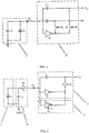
- the I-V conversion module includes: a current output type sensor 1, an I-V transformation circuit 2 including an inverting amplifier X 1 , a charge transfer auxiliary circuit 3, and a pre-integral circuit 4.
- the current output type sensor 1 is connected to an input end V in of the I-V transformation circuit 2 via the pre-integral circuit 4; and the charge transfer auxiliary circuit 3 is connected in parallel with the inverting amplifier X 1 .
- the I-V transformation circuit 2 also includes a transformation branch which includes an integral energy storage element C 1 and an integral switch S 1 .
- a first end of the integral energy storage element C 1 is connected to an input end of the inverting amplifier X 1 and forms an input end V in of the I-V transformation circuit;
- a second end of the integral energy storage element C 1 is connected to the first end of the integral switch S 1 and forms an output end V OP of the I-V transformation circuit 2;
- the output end of the inverting amplifier X 1 is connected to the second end of the integral switch S 1 .
- the integral energy storage element is a capacitor.
- the integral energy storage element is not limited to this, and it can be applied to other integral energy storage elements.
- the charge transfer auxiliary circuit 3 includes a plurality of inverting amplifiers X 2 that are connected in parallel with each other.
- the charge transfer auxiliary circuit 3 can be switched on by enabling or disabling the inverting amplifiers X 2 .
- each inverting amplifier X 2 is connected to the input end of the inverting amplifier X 1
- an output end of each inverting amplifier X2 is connected to the output end of the inverting amplifier X 1 and the second end of the integral switch S 1 .
- a plurality of inverting amplifiers X 2 are used to provide sufficient gain-bandwidth product to transfer charges.
- N is greater than 1 and is an integer.
- the number of N of the inverting amplifier X 2 relates to a gain multiplier of the I-V conversion circuit. The greater the gain multiplier, the greater the number N of the inverting amplifier X 2 .
- there is no limit to the number N of the inverting amplifier X 2 there is no limit to the number N of the inverting amplifier X 2 , and it may be set according to practical situations.
- the pre-integral circuit 4 includes a pre-integral energy storage unit and a pre-integral switch S 3 .
- One end of the pre-integral energy storage unit is connected to a first end of a pre-integral switch S3 and the current output type sensor 1, and the other end of the pre-integral energy storage unit is grounded GNDo.
- the second end of the pre-integral switch S 3 is connected to the input end V in of the I-V transformation circuit 2.
- the pre-integral energy storage unit includes a coupling capacitor C 0 of the current output type sensor 1 per se.
- the inverting amplifier (X1 or X2) includes an inverter or an operational amplifier, to which this embodiment does not put any limit.
- ⁇ 1 is a two-phase non-overlapping clock
- a clock signal ⁇ 3 controls the conduction of the inverting amplifier X 2 with the pre-integral switch S 3 .
- ⁇ 1 1 as an example to illustrate the working process of the I-V conversion module.
- the integral switch S 1 is on and the pre-integral switch S 3 is off.
- the inverter amplifier X 1 works.
- both the pre-integral circuit 4 and the charge transfer auxiliary circuit 3 are open circuits, and the pre-integral circuit 4 pre-integrates the induction current I 0 output by the current output type sensor 1. That is, the coupling capacitor C 0 pre-integrates the induction current I 0 to store the pre-integral charges.
- the inverting amplifier X 2 does not work, and the inverting amplifier X 1 forms a negative feedback loop with the capacitor C 1 , thereby maintaining the charges in the capacitor C 1 .
- the integral switch S 1 is on, and the pre-integral switch S 3 is on.
- both the pre-integral circuit 4 and the charge transfer auxiliary circuit 3 are closed circuit; the inverting amplifier X2 provides a sufficient gain-bandwidth product, and the pre-integral charges are transferred to the I-V transformation circuit 2. That is, the pre-integral charge is transferred from the coupling capacitor C 0 to the integral energy storage element C 1 , and is kept by the integral energy storage element C 1 .
- the voltage of the input end V in of the I-V transformation circuit 2 is restored to the voltage at the middle point of the inverting amplifier X 1 .
- the horizontal axis X represents a response time
- the y axis represents an amplitude of the output voltage
- the dotted line represents an output response of an existing conventional I-V conversion module
- the solid line represents an output response of the I-V conversion module of the present disclosure.
- the total power consumption of the inverting amplifier X 1 and the inverting amplifier X 2 is equal to the total power consumption of the inverting amplifier in the existing conventional I-V conversion module.
- the inverting amplifier has been in a working state in the existing conventional I-V conversion module, that is, the inverting amplifier has been consuming energy.
- the inverting amplifier X 1 and the inverting amplifier X 2 work simultaneously during the A 1 time period; the inverting amplifier X 1 works and the inverting amplifier X 2 does not work during the A 2 time period.
- the I-V conversion module in this embodiment greatly reduces the total power consumption.
- the A1 time period is 1/10 of the A2 time period. That is, the conversion mode takes up only 1/10 of the time of the power saving mode. Therefore, the inverting amplifier X 1 works with the inverting amplifier X 2 for a very short time, and the power consumption is very low. It can be generally assumed that the average power consumption by the I-V conversion module in this embodiment is only 1/10 of an average power consumption by the existing conventional I-V conversion module.
- the I-V conversion module includes a pre-integration circuit and a charge transfer auxiliary circuit. It takes only 1/10 of the existing time required to pre-integrate the induction current by using the parasitic capacitor of the current type sensor, and to transfer the pre-integral charge to the I-V transformation circuit by using the gain-bandwidth product provided by the inverting amplifier, so that the I-V conversion module establishes the same output voltage as the existing I-V conversion module does.
- the average power consumption by the I-V conversion module in this embodiment may be only 1/10 of the average power consumption by the existing I-V conversion module, thereby greatly reducing the power consumption.
- a second embodiment of the present disclosure relates to an I-V conversion module.
- the second embodiment is generally the same as the first embodiment, and the main difference is that the number of transformation branches is 1 in the I-V transformation circuit in the first embodiment. As shown in Fig. 5 , the number of transformation branches is 2 in the second embodiment of the present disclosure.
- an additional transformation branch includes the integral energy storage element C 2 and the integral switch S 2 .
- the first end of the integral energy storage element C 2 is connected to the input end of the inverting amplifier X 1 ; the second end of the integral energy storage element C 2 is connected to the first end of the integral switch S 2 and forms another output end V on of the I-V transform circuit; the second end of the integral switch S 2 is connected to the output end of the inverting amplifier X 1 .
- FIG. 6 there is a control sequence diagram.
- ⁇ 1 and ⁇ 2 are two-phase non-overlapping clocks.
- this embodiment does not put any limit to the number of the transformation branches, and the M transformation branches can be set as desired, M being a positive integer greater than zero.
- this embodiment applies two transformation branches in the I-V transformation circuit and each transformation branch can output differential voltage signals, which can enable the differential output characteristic, and facilitate subsequent demodulation of the signals through positive and negative cancellation. This allows to be more widely applied.
- a third embodiment of the present disclosure relates to an I-V conversion module.
- the third embodiment is improved on the basis of the second embodiment, and the main improvement is that in the third embodiment of the present disclosure, as shown in FIG. 7 , the pre-integral energy storage unit can include an adjustable energy storage element C 3 in the pre-integral circuit 4.
- the adjustable energy storage element C 3 is connected in parallel with the coupling capacitor C 0 . That is, one end of the adjustable energy storage element C 3 is connected to the first end of the coupling capacitor C 0 and the pre-integral switch S 3 , and the other end is grounded (connected to GND 1 ).
- the adjustable energy storage element C 3 is an adjustable capacitor, but in practice, the adjustable energy storage element C 3 may include any components with energy storage functions.
- the capacitance of the adjustable energy storage element C 3 is related to the capacitance of the coupling capacitor C 0 and the induction current I 0 .
- This embodiment does not put any limit to the specific capacitance of the adjustable capacitance C 3 which can be adjusted according to the actual situations.
- the adjustable energy storage elements in the pre-integral circuit can improve energy storage capacity of the pre-integral energy storage unit.
- the pre-integration switch When disconnected, it can smooth out the magnitude drop of the input voltage of the I-V transform circuit. That is, the adjustable energy storage element can reduce the nonlinearity of the current output type sensor.
- the fourth embodiment of the present disclosure relates to an I-V conversion module.
- the fourth embodiment is improved on the basis of the third embodiment, and the main improvement is that in the fourth embodiment of the present disclosure, as shown in FIG. 8 , the I-V transformation circuit also includes a reset switch S 4 .
- the reset switch S 4 is connected in parallel with the inverting amplifier X 1 . That is, the first end of the reset switch S 4 is connected to the input end of the inverting amplifier X 1 , and the second end of the reset switch S 4 is connected to the output end of the inverting amplifier X 1 . In practice, the reset switch S 4 is also connected in parallel with the inverting amplifier X 2 .
- a reset switch is added in the I-V transformation circuit, so that the charges in the I-V transformation circuit may conveniently be cleared to meet requirements for detection.
- a logical unit can be a physical unit, a part of a physical unit, or a combination of multiple physical units.
- a unit that is not closely related to the technical problems proposed by the present disclosure has not been introduced in the above embodiments, but it does not mean that there are no other units in the embodiments.
- the computer programs are stored in a storage medium, including a number of instructions to cause a device (which can be microcontrollers, a chip, etc.) or a processor to execute all or some steps of the method described in each embodiment.
- the previous storage media includes media such as a U disk, a mobile hard disk, a read-only memory (ROM), a random access memory (RAM), a magnetic disc or a disc, which can store computer programs codes.
Landscapes
- Engineering & Computer Science (AREA)
- Power Engineering (AREA)
- Physics & Mathematics (AREA)
- Multimedia (AREA)
- Electromagnetism (AREA)
- General Physics & Mathematics (AREA)
- Computer Hardware Design (AREA)
- Computing Systems (AREA)
- General Engineering & Computer Science (AREA)
- Mathematical Physics (AREA)
- Amplifiers (AREA)
Abstract
Description
- The present disclosure relates to the field of electronic technologies and, more particularly, to an I-V conversion module.
- As shown in
FIG. 1 , an existing current-voltage conversion module, i.e., an I-V conversion module, is composed of acurrent output sensor 1" and anI-V transformation circuit 2". The larger the open-loop gain of the inverting amplifier X, the larger the bandwidth, and the faster the response time of theI-V transformation circuit 2". - As shown in
FIG. 1 , ϕ1 and ϕ2 are two-phase non-overlapping clocks. As theI-V transformation circuit 2" is of a symmetric structure, the working process of the I-V conversion module is illustrated by an example of ϕ1=1 (An example of ϕ2=1 can be understood in a same way). When ϕ1=1, a switch S1 is switched on, a capacitor C1 forms a negative feedback loop with the inverting amplifier X, and an input voltage of theI-V transformation circuit 2" is constantly a middle point voltage of the inverting amplifier X. Thus, an output current I0 of thecurrent type sensor 1" does not flow through a parasitic capacitor C0 of the sensor and flows through the capacitor C1. - If A0 is a low-frequency open-loop gain of the amplifier, p is a bandwidth, s is a Laplace operator, and Vop is an output voltage of a branch of the
I-V transformation circuit 2. With the assumption that the open-loop gain of the inverting amplifier X is A(s) = A0p/(s+p), a transfer function of the I-V conversion module can be obtained:
- An input step signal can be derived from the
formula 1, and expression of a response of the output I-V transformation circuit is:
- The inventor finds the following issue in the existing technologies: it is seen from
Formula 2 that the low-frequency open-loop gain A0 and the bandwidth P of the amplifier can affect the response time of the I-V transformation circuit, which results a longer response time of the I-V transformation circuit. In order to solve this issue, it is necessary to increase the open loop gain A(s) and -3dB bandwidth p of the inverting amplifier X. In other words, the inverting amplifier X shall have a sufficiently large gain-bandwidth product (usually 10 times the inverse of the I-V conversion time). However, according to the theory, when the gain-bandwidth product increases by 2 times, power consumption of the inverting amplifier X increases by 4 times. As a result, although the method may meet the needs for establishing an I-V conversion module, power consumption by the inverting amplifier X is too high. - Some embodiments of the present disclosure aim at providing an I-V conversion module, which requires less time for establishing the I-V conversion module with lower power consumption.
- To solve the above technical problem, some embodiments of the present disclosure provide an I-V conversion module, which comprises a current output type sensor, a pre-integral circuit, a charge transfer auxiliary circuit, and an I-V transformation circuit including an inverting amplifier; the current output type sensor connects to an input end of the I-V transformation circuit through the pre-integral circuit; the charge transfer auxiliary circuit connects in parallel with the inverting amplifier; wherein when both the pre-integral circuit and the charge transfer auxiliary circuit are open circuits, the pre-integral circuit pre-integrates the induction current that is output by the current output type sensor so as to store pre-integral charges; when both pre-integral circuit and the charge transfer auxiliary circuit are closed circuit, the pre-integral charges are transferred to the I-V transformation circuit.
- In some embodiments of the present disclosure, compared with the existing technologies, the I-V conversion module includes a pre-integral circuit and a charge transfer auxiliary circuit. The pre-integral circuit is used to pre-integrate an induction current, and the pre-integral charges can be quickly transferred to the I-V transformation circuit by using the gain-bandwidth product of the inverting amplifier. Consequently, the I-V conversion module requires less time when the I-V conversion module establishes an output voltage that is the same as an existing I-V conversion module. Further, power consumption can be greatly reduced by some embodiments of the present disclosure.
- Optionally, a pre-integral energy storage unit may include an adjustable energy storage element which is connected in parallel with the coupling capacitor. In this embodiment, the adjustable energy storage element can increase energy storage capacity of the pre-integral energy storage unit; when a pre-integral switch is disconnected, it can smooth out a magnitude drop of the input voltage of the I-V transformation circuit. That is, the adjustable energy storage element can reduce nonlinearity of the current output type sensor.
- Optionally, the number of the transformation branches is 2. In this embodiment, two transformation branches can output differential voltage signals to realize differential output characteristics and facilitate subsequent demodulation of signals through positive and negative cancellation. This can be widely applied..
- Optionally, the I-V transformation circuit also can include a reset switch which is connected in parallel with the inverting amplifier. In this embodiment, the reset switch is added to facilitate clearance of charges in the I-V transformation circuit so as to meet the requirements for detection.
- One or more embodiments are exemplified by the corresponding figures in the accompanying drawings, which do not put a limit to the embodiment, and the elements with the same reference numbers in the drawings are expressed as similar elements. The figures in the accompanying drawings do not present a proportional limit unless specifically declared.
-
FIG. 1 is a schematic diagram of an I-V conversion module in related art. -
FIG. 2 is a schematic diagram of the I-V conversion module according to a first embodiment of the present disclosure. -
FIG. 3 is a schematic diagram of timing control of the I-V conversion module according to the first embodiment. -
FIG. 4 is a curve diagram of comparison between output step responses in the I-V conversion module in the first embodiment and output step responses in the I-V conversion module in the related art; -
FIG. 5 is a schematic diagram of the I-V conversion module according to a second embodiment of the present disclosure; -
FIG. 6 is a schematic diagram of timing control of the I-V conversion module according to the second embodiment; -
FIG. 7 is a schematic diagram of the I-V conversion module according to a third embodiment of the present disclosure; -
FIG. 8 is a schematic diagram of the I-V conversion module according to a fourth embodiment of the present disclosure. - In order to make a purpose, a technical solution and advantages of the present disclosure clearer, some embodiments of the invention will be described in detail in accordance with the drawings. However, those ordinarily skilled in the art can understand that in the various embodiments of the invention, many technical details are proposed to enable a reader to better understand the application. However, even without these technical details and changes and modifications to the following embodiments, the technical solutions claimed for protection in this application can still be realized.
- A first embodiment of the present disclosure provides an I-V conversion module. As shown in
FIG. 2 , the I-V conversion module includes: a currentoutput type sensor 1, anI-V transformation circuit 2 including an inverting amplifier X1, a charge transferauxiliary circuit 3, and apre-integral circuit 4. - In this embodiment, the current
output type sensor 1 is connected to an input end Vin of theI-V transformation circuit 2 via thepre-integral circuit 4; and the charge transferauxiliary circuit 3 is connected in parallel with the inverting amplifier X1. - In this embodiment, as shown in
FIG. 2 , theI-V transformation circuit 2 also includes a transformation branch which includes an integral energy storage element C1 and an integral switch S1. A first end of the integral energy storage element C1 is connected to an input end of the inverting amplifier X1 and forms an input end Vin of the I-V transformation circuit; a second end of the integral energy storage element C1 is connected to the first end of the integral switch S1 and forms an output end VOP of theI-V transformation circuit 2; the output end of the inverting amplifier X1 is connected to the second end of the integral switch S1. - In this embodiment, the integral energy storage element is a capacitor. However, in fact it is not limited to this, and it can be applied to other integral energy storage elements.
- In this embodiment, the charge transfer
auxiliary circuit 3 includes a plurality of inverting amplifiers X2 that are connected in parallel with each other. The charge transferauxiliary circuit 3 can be switched on by enabling or disabling the inverting amplifiers X2. - Specifically, an input end of each inverting amplifier X2 is connected to the input end of the inverting amplifier X1, and an output end of each inverting amplifier X2 is connected to the output end of the inverting amplifier X1 and the second end of the integral switch S1.
- It should be noted that in this embodiment, a plurality of inverting amplifiers X2 are used to provide sufficient gain-bandwidth product to transfer charges. When the number of the inverting amplifiers X2 is N, N is greater than 1 and is an integer. The number of N of the inverting amplifier X2 relates to a gain multiplier of the I-V conversion circuit. The greater the gain multiplier, the greater the number N of the inverting amplifier X2. In this embodiment, there is no limit to the number N of the inverting amplifier X2, and it may be set according to practical situations.
- In this embodiment, the
pre-integral circuit 4 includes a pre-integral energy storage unit and a pre-integral switch S3. One end of the pre-integral energy storage unit is connected to a first end of a pre-integral switch S3 and the currentoutput type sensor 1, and the other end of the pre-integral energy storage unit is grounded GNDo. The second end of the pre-integral switch S3 is connected to the input end Vin of theI-V transformation circuit 2. In this embodiment, the pre-integral energy storage unit includes a coupling capacitor C0 of the currentoutput type sensor 1 per se. - In this embodiment, the inverting amplifier (X1 or X2) includes an inverter or an operational amplifier, to which this embodiment does not put any limit.
- In this embodiment, as shown in
FIG. 2 andFIG. 3 , ϕ1 is a two-phase non-overlapping clock, and a clock signal ϕ3 controls the conduction of the inverting amplifier X2 with the pre-integral switch S3. Next, take ϕ1=1 as an example to illustrate the working process of the I-V conversion module. - Specifically, when
ϕ l1=1 and ϕ3=0, the integral switch S1 is on and the pre-integral switch S3 is off. The inverter amplifier X1 works. At this time, both thepre-integral circuit 4 and the charge transferauxiliary circuit 3 are open circuits, and thepre-integral circuit 4 pre-integrates the induction current I0 output by the currentoutput type sensor 1. That is, the coupling capacitor C0 pre-integrates the induction current I0 to store the pre-integral charges. At the same time, the inverting amplifier X2 does not work, and the inverting amplifier X1 forms a negative feedback loop with the capacitor C1, thereby maintaining the charges in the capacitor C1. - Specifically, when ϕ1=1 and ϕ3=1, the integral switch S1 is on, and the pre-integral switch S3 is on. At this time, both the
pre-integral circuit 4 and the charge transferauxiliary circuit 3 are closed circuit; the inverting amplifier X2 provides a sufficient gain-bandwidth product, and the pre-integral charges are transferred to theI-V transformation circuit 2. That is, the pre-integral charge is transferred from the coupling capacitor C0 to the integral energy storage element C1, and is kept by the integral energy storage element C1. The voltage of the input end Vin of theI-V transformation circuit 2 is restored to the voltage at the middle point of the inverting amplifier X1. - Generally, in this embodiment, the conversion process of the I-V conversion module can be deemed as an equivalent of inputting a step response between 0 and I0Tint/(C0+C3) to a ground plate of a coupling capacitor C0, wherein Tint is pre-integration time. Therefore, the step response expression of the process can be obtained as follows:

- Suppose the pre-integration time is Tint=10uS, C0=50pF, C1=100pF, p=100 rad/s, A0=10k. These parameters can be applied to the
formula 2 andformula 3 in the present disclosure, and the curves can be drawn as shown inFIG. 4 to respectively correspond to the curves of the output step response of the I-V conversion module inFIG. 1 and FIG. 2 . - As shown in
FIG. 4 , the horizontal axis X represents a response time, and the y axis represents an amplitude of the output voltage; the dotted line represents an output response of an existing conventional I-V conversion module, and the solid line represents an output response of the I-V conversion module of the present disclosure. It can be seen that the I-V conversion module sets up a same output voltage as compared with the existing conventional I-V conversion module, e.g., establishing a voltage of 0.01V. The existing conventional I-V conversion module needs 10-5Us, while the I-V conversion module of this embodiment only needs 0.1*10-5Us. It is clear that the time required by the I-V conversion module is only 1/10 of the time required by a conventional I-V conversion module. - In this embodiment, the total power consumption of the inverting amplifier X1 and the inverting amplifier X2 is equal to the total power consumption of the inverting amplifier in the existing conventional I-V conversion module. As shown in
FIG. 3 , in the A1 and A2 time periods, the inverting amplifier has been in a working state in the existing conventional I-V conversion module, that is, the inverting amplifier has been consuming energy. In the I-V conversion module of the embodiment of this invention, the inverting amplifier X1 and the inverting amplifier X2 work simultaneously during the A1 time period; the inverting amplifier X1 works and the inverting amplifier X2 does not work during the A2 time period. Accordingly, in this embodiment, only the inverting amplifier X1 has power consumption during the A2 time period, and the overall I-V conversion module needs less power consumption as compared with that in the existing technologies. That is, the entire I-V conversion module during the A2 time period is in a power-saving mode. Therefore, compared with the existing conventional I-V conversion module, the I-V conversion module in this embodiment greatly reduces the total power consumption. Further, in this embodiment, the A1 time period is 1/10 of the A2 time period. That is, the conversion mode takes up only 1/10 of the time of the power saving mode. Therefore, the inverting amplifier X1 works with the inverting amplifier X2 for a very short time, and the power consumption is very low. It can be generally assumed that the average power consumption by the I-V conversion module in this embodiment is only 1/10 of an average power consumption by the existing conventional I-V conversion module. - In this embodiment, compared with the existing technologies, the I-V conversion module includes a pre-integration circuit and a charge transfer auxiliary circuit. It takes only 1/10 of the existing time required to pre-integrate the induction current by using the parasitic capacitor of the current type sensor, and to transfer the pre-integral charge to the I-V transformation circuit by using the gain-bandwidth product provided by the inverting amplifier, so that the I-V conversion module establishes the same output voltage as the existing I-V conversion module does. Besides, the average power consumption by the I-V conversion module in this embodiment may be only 1/10 of the average power consumption by the existing I-V conversion module, thereby greatly reducing the power consumption.
- A second embodiment of the present disclosure relates to an I-V conversion module. The second embodiment is generally the same as the first embodiment, and the main difference is that the number of transformation branches is 1 in the I-V transformation circuit in the first embodiment. As shown in
Fig. 5 , the number of transformation branches is 2 in the second embodiment of the present disclosure. - In this embodiment, an additional transformation branch includes the integral energy storage element C2 and the integral switch S2. The first end of the integral energy storage element C2 is connected to the input end of the inverting amplifier X1; the second end of the integral energy storage element C2 is connected to the first end of the integral switch S2 and forms another output end Von of the I-V transform circuit; the second end of the integral switch S2 is connected to the output end of the inverting amplifier X1.
- In this embodiment, as shown in
FIG. 6 there is a control sequence diagram. ϕ1 and ϕ2 are two-phase non-overlapping clocks. TheI-V transform circuit 2 is of a symmetric structure. Therefore, for ϕ2=1, the working process can be obtained according to the same conditions of ϕ1=1. Specifically, the working process of the I-V conversion module for ϕ1=1 can be understood by reference to the first embodiment, and will not be repeated. - In fact, in the
I-V transformation circuit 2, this embodiment does not put any limit to the number of the transformation branches, and the M transformation branches can be set as desired, M being a positive integer greater than zero. - As compared with the first embodiment, this embodiment applies two transformation branches in the I-V transformation circuit and each transformation branch can output differential voltage signals, which can enable the differential output characteristic, and facilitate subsequent demodulation of the signals through positive and negative cancellation. This allows to be more widely applied.
- A third embodiment of the present disclosure relates to an I-V conversion module. The third embodiment is improved on the basis of the second embodiment, and the main improvement is that in the third embodiment of the present disclosure, as shown in
FIG. 7 , the pre-integral energy storage unit can include an adjustable energy storage element C3 in thepre-integral circuit 4. - In this embodiment, the adjustable energy storage element C3 is connected in parallel with the coupling capacitor C0. That is, one end of the adjustable energy storage element C3 is connected to the first end of the coupling capacitor C0 and the pre-integral switch S3, and the other end is grounded (connected to GND1).
- In this embodiment, as shown in
FIG. 7 , the adjustable energy storage element C3 is an adjustable capacitor, but in practice, the adjustable energy storage element C3 may include any components with energy storage functions. - It shall be noted that in this embodiment, the capacitance of the adjustable energy storage element C3 is related to the capacitance of the coupling capacitor C0 and the induction current I0. The larger the coupling capacitor C0 and the smaller the induction current I0, the larger the adjustable energy storage element C3. Therefore, the adjustable energy storage element C3 can be adjusted in the range of [0, ∞) in accordance with the capacitance of the coupling capacitor C0 and the induction current I0. This embodiment does not put any limit to the specific capacitance of the adjustable capacitance C3 which can be adjusted according to the actual situations.
- In the embodiment of the present disclosure, compared with the second embodiment, by adding the adjustable energy storage elements in the pre-integral circuit can improve energy storage capacity of the pre-integral energy storage unit. When the pre-integration switch is disconnected, it can smooth out the magnitude drop of the input voltage of the I-V transform circuit. That is, the adjustable energy storage element can reduce the nonlinearity of the current output type sensor.
- The fourth embodiment of the present disclosure relates to an I-V conversion module. The fourth embodiment is improved on the basis of the third embodiment, and the main improvement is that in the fourth embodiment of the present disclosure, as shown in
FIG. 8 , the I-V transformation circuit also includes a reset switch S4. - In this embodiment, the reset switch S4 is connected in parallel with the inverting amplifier X1. That is, the first end of the reset switch S4 is connected to the input end of the inverting amplifier X1, and the second end of the reset switch S4 is connected to the output end of the inverting amplifier X1. In practice, the reset switch S4 is also connected in parallel with the inverting amplifier X2.
- In the embodiment of the present disclosure, compared with the third embodiment, a reset switch is added in the I-V transformation circuit, so that the charges in the I-V transformation circuit may conveniently be cleared to meet requirements for detection.
- It is worth mentioning that all the modules involved in this embodiment are logical modules. In practical applications, a logical unit can be a physical unit, a part of a physical unit, or a combination of multiple physical units. In addition, in order to explain the present disclosure, a unit that is not closely related to the technical problems proposed by the present disclosure has not been introduced in the above embodiments, but it does not mean that there are no other units in the embodiments.
- Those skilled in the art can understand that all or part of the steps in the methods of the above-mentioned embodiments can be achieved by execution of computer programs to instruct hardware to perform one or more steps. The computer programs are stored in a storage medium, including a number of instructions to cause a device (which can be microcontrollers, a chip, etc.) or a processor to execute all or some steps of the method described in each embodiment. The previous storage media includes media such as a U disk, a mobile hard disk, a read-only memory (ROM), a random access memory (RAM), a magnetic disc or a disc, which can store computer programs codes.
- It is understandable to those ordinary skilled in the art that the above embodiments are specific examples in the present disclosure, and in practical applications, various changes can be made in form and in detail without deviating from the spirit and scope of the present disclosure.
Claims (10)
- An I-V conversion module, characterized by comprising: a current output type sensor, a pre-integral circuit, a charge transfer auxiliary circuit, and an I-V transformation circuit comprising an inverting amplifier;wherein the current output type sensor connects to an input end of the I-V transformation circuit through the pre-integral circuit;wherein the charge transfer auxiliary circuit connects in parallel with the inverting amplifier;wherein when both the pre-integral circuit and the charge transfer auxiliary circuit are open circuits, the pre-integral circuit pre-integrates the induction current that is output by the current output type sensor so as to store pre-integral charges; when both the pre-integral circuit and the charge transfer auxiliary circuit are closed circuits, the pre-integral charges are transferred to the I-V transformation circuit.
- The I-V conversion module according to claim 1, characterized in that the pre-integral circuit comprises a pre-integral energy storage unit and a pre-integral switch;wherein one end of the pre-integral energy storage unit connects to a first end of the pre-integral switch and the current output type sensor; the other end of the pre-integral energy storage unit is grounded;wherein the second end of the pre-integral switch connects to the input end of the I-V transformation circuit;wherein the pre-integral energy storage unit at least comprises a coupling capacitor of the current output type sensor.
- The I-V conversion module according to claim 2, characterized in that the pre-integral energy storage unit comprises an adjustable energy storage element;wherein the adjustable energy storage element connects in parallel with the coupling capacitor.
- The I-V conversion module according to claim 3, characterized in that the adjustable energy storage element comprises an adjustable capacitor.
- The I-V conversion module according to claim 1, characterized in that the I-V transformation circuit comprises at least one transformation branch, each transformation branch comprises an integral energy storage element and an integral switch;wherein the first end of the integral energy storage element connects to the input end of the inverting amplifier, and forms the input end of the I-V transformation circuit;wherein the second end of the integral energy storage element connects to the first end of the integral switch, and forms an output end of the I-V transformation circuit;wherein an output end of the inverting amplifier connects to the second end of the integral switch.
- The I-V conversion module according to claim 5, characterized in that the integral energy storage element comprises a capacitor.
- The I-V conversion module according to claim 5, characterized in that the number of the transformation branches is 2.
- The I-V conversion module according to claim 1, characterized in that the charge transfer auxiliary circuit comprises a plurality of inverting amplifiers that are connected in parallel with each other.
- The I-V conversion module according to any one of claims 1 to 8, characterized in that the inverting amplifier comprises an inverter or an operational amplifier.
- The I-V conversion module according to claim 1, characterized in that the I-V transformation circuit further comprises a reset switch, the reset switch is connected in parallel with the inverting amplifier.
Applications Claiming Priority (1)
| Application Number | Priority Date | Filing Date | Title |
|---|---|---|---|
| PCT/CN2016/107205 WO2018094681A1 (en) | 2016-11-25 | 2016-11-25 | I-v conversion module |
Publications (2)
| Publication Number | Publication Date |
|---|---|
| EP3402076A1 true EP3402076A1 (en) | 2018-11-14 |
| EP3402076A4 EP3402076A4 (en) | 2019-04-10 |
Family
ID=62194587
Family Applications (1)
| Application Number | Title | Priority Date | Filing Date |
|---|---|---|---|
| EP16922161.1A Ceased EP3402076A4 (en) | 2016-11-25 | 2016-11-25 | I-V CONVERSION MODULE |
Country Status (4)
| Country | Link |
|---|---|
| US (1) | US10727791B2 (en) |
| EP (1) | EP3402076A4 (en) |
| CN (1) | CN109075792B (en) |
| WO (1) | WO2018094681A1 (en) |
Families Citing this family (1)
| Publication number | Priority date | Publication date | Assignee | Title |
|---|---|---|---|---|
| CN115037275B (en) * | 2022-05-23 | 2026-04-07 | 广东人工智能与先进计算研究院 | An RC low-pass filter and a fast filter establishment method |
Family Cites Families (22)
| Publication number | Priority date | Publication date | Assignee | Title |
|---|---|---|---|---|
| JPS5933912A (en) * | 1982-08-18 | 1984-02-24 | Nippon Telegr & Teleph Corp <Ntt> | Current voltage converting circuit |
| US4902886A (en) * | 1989-01-23 | 1990-02-20 | Hewlett-Packard Company | Noise reduction for photodiode arrays |
| US5367302A (en) * | 1993-08-24 | 1994-11-22 | Burr-Brown Corporation | Isolating a CDAC array in a current integrating ADC |
| US6150851A (en) * | 1997-06-06 | 2000-11-21 | Tadahiro Ohmi | Charge transfer amplifier circuit, voltage comparator, and sense amplifier |
| TW550447B (en) * | 2000-10-30 | 2003-09-01 | Realtek Semiconductor Corp | Signal generator with adjustable oscillation frequency and its method |
| JP3940616B2 (en) * | 2002-02-25 | 2007-07-04 | 松下電器産業株式会社 | Optical receiver circuit |
| US7400121B2 (en) * | 2002-08-06 | 2008-07-15 | Texas Instruments Incorporated | Soft-start system for voltage regulator and method of implementing soft-start |
| GB2423429B (en) * | 2003-10-10 | 2007-04-25 | That Corp | Low-power integrated-circuit signal processor with wide dynamic range |
| US8159204B2 (en) * | 2008-09-29 | 2012-04-17 | Active-Semi, Inc. | Regulating current output from a buck converter without external current sensing |
| CN102362449B (en) * | 2009-02-23 | 2015-09-09 | 惠普开发有限公司 | Dynamic Impedance Photodetector Receiver Circuit |
| US7936299B2 (en) * | 2009-06-30 | 2011-05-03 | General Electric Company | Capacitive integrate and fold charge-to-digital converter |
| US8120439B2 (en) * | 2009-08-13 | 2012-02-21 | Texas Instruments Incorporated | Fast start-up crystal oscillator |
| CN102566641B (en) * | 2010-12-07 | 2014-03-26 | 联咏科技股份有限公司 | Low-noise current buffer circuit and current-voltage converter |
| CN202085151U (en) * | 2011-03-10 | 2011-12-21 | 上海信诚电子技术工程有限公司 | Current-to-voltage (I/V) converter circuit |
| FR2981229B1 (en) * | 2011-10-10 | 2013-12-27 | Commissariat Energie Atomique | DEVICE FOR CONVERTING CURRENT PULSES TO VOLTAGE PULSES. |
| US8593218B2 (en) * | 2011-11-08 | 2013-11-26 | Analog Devices, Inc. | Fast settling low power low noise amplifier |
| CN102651633B (en) * | 2012-05-15 | 2014-09-10 | 江苏科技大学 | Noise current feed-forward type noise cancellation circuit |
| US20140177304A1 (en) * | 2012-12-24 | 2014-06-26 | Laurence P. Sadwick | Constant Current Source |
| CN103383404B (en) * | 2013-07-04 | 2015-11-25 | 清华大学 | Current measurement circuit |
| CN103364614B (en) * | 2013-07-14 | 2015-10-28 | 中国科学院近代物理研究所 | Self-adaptation wide-range current/voltage conversion equipment |
| EP3059857B1 (en) * | 2015-02-17 | 2021-11-03 | Nxp B.V. | Time to digital converter and phase locked loop |
| CN105406829B (en) * | 2015-12-03 | 2018-02-27 | 中国科学院电子学研究所 | A kind of variable gain amplifier of gain continuously adjustabe |
-
2016
- 2016-11-25 EP EP16922161.1A patent/EP3402076A4/en not_active Ceased
- 2016-11-25 WO PCT/CN2016/107205 patent/WO2018094681A1/en not_active Ceased
- 2016-11-25 CN CN201680001576.7A patent/CN109075792B/en active Active
-
2018
- 2018-08-07 US US16/057,216 patent/US10727791B2/en active Active
Also Published As
| Publication number | Publication date |
|---|---|
| WO2018094681A1 (en) | 2018-05-31 |
| CN109075792B (en) | 2022-04-01 |
| CN109075792A (en) | 2018-12-21 |
| US20180375481A1 (en) | 2018-12-27 |
| EP3402076A4 (en) | 2019-04-10 |
| US10727791B2 (en) | 2020-07-28 |
Similar Documents
| Publication | Publication Date | Title |
|---|---|---|
| EP2686945B1 (en) | Charge pump surge current reduction | |
| US10658061B2 (en) | Shift register circuit, method for driving shift register circuit, gate electrode driving circuit and display device | |
| US20180123452A1 (en) | Charge recycling switched capacitor regulators | |
| DE112016001067T5 (en) | Radio frequency system switching power amplifier systems and methods | |
| CN106094525A (en) | A kind of TSM control device based on fractional calculus and control method | |
| US4931745A (en) | Low noise chopper stabilized amplifier and method of operation | |
| CN102594299B (en) | Square-wave generator circuit | |
| Cheng et al. | Neuroadaptive finite-time output feedback control for PMSM stochastic nonlinear systems with iron losses via dynamic surface technique | |
| CN106026960A (en) | Serial capacitance tuner | |
| CN102480270B (en) | Power amplifier and MMIC using the same | |
| US10727791B2 (en) | I—V conversion module | |
| CN113485518A (en) | A Universal LDO Transient Response Enhancement Circuit | |
| CN114758702B (en) | Memristor value accurate writing circuit | |
| CN119276226B (en) | A BUCK converter and a variable gain error amplifier circuit | |
| CN105096857B (en) | A kind of gate driving circuit and liquid crystal display | |
| CN113447697B (en) | Signal detection circuit, signal detection method, touch panel and display device | |
| CN212588305U (en) | Power amplification circuit and detection terminal | |
| GB2157108A (en) | Eliminating input offset | |
| CN109462376A (en) | A kind of three rank amplifier of frequency compensation | |
| CN115562417A (en) | Slew rate adjusting circuit, method and chip | |
| CN210246702U (en) | Charge amplifier circuit | |
| CN210693873U (en) | Automatic correction circuit for output offset voltage of class-D power amplifier circuit | |
| CN105242735A (en) | Asymmetric voltage stabilizing circuit used for NAND FLASH | |
| CN115514231B (en) | Control methods, control circuits, controllers, and control systems | |
| Chien et al. | Adaptive variable structure control |
Legal Events
| Date | Code | Title | Description |
|---|---|---|---|
| STAA | Information on the status of an ep patent application or granted ep patent |
Free format text: STATUS: THE INTERNATIONAL PUBLICATION HAS BEEN MADE |
|
| PUAI | Public reference made under article 153(3) epc to a published international application that has entered the european phase |
Free format text: ORIGINAL CODE: 0009012 |
|
| STAA | Information on the status of an ep patent application or granted ep patent |
Free format text: STATUS: REQUEST FOR EXAMINATION WAS MADE |
|
| 17P | Request for examination filed |
Effective date: 20180807 |
|
| AK | Designated contracting states |
Kind code of ref document: A1 Designated state(s): AL AT BE BG CH CY CZ DE DK EE ES FI FR GB GR HR HU IE IS IT LI LT LU LV MC MK MT NL NO PL PT RO RS SE SI SK SM TR |
|
| AX | Request for extension of the european patent |
Extension state: BA ME |
|
| A4 | Supplementary search report drawn up and despatched |
Effective date: 20190307 |
|
| RIC1 | Information provided on ipc code assigned before grant |
Ipc: H03G 1/00 20060101ALI20190301BHEP Ipc: H03F 1/42 20060101ALI20190301BHEP Ipc: H03F 3/72 20060101ALI20190301BHEP Ipc: H03F 3/70 20060101ALI20190301BHEP Ipc: H03G 3/00 20060101ALI20190301BHEP Ipc: H03G 5/12 20060101ALI20190301BHEP Ipc: G05F 1/565 20060101ALI20190301BHEP Ipc: G01B 15/00 20060101ALI20190301BHEP Ipc: H03F 3/00 20060101ALI20190301BHEP Ipc: H03G 3/30 20060101ALI20190301BHEP Ipc: H03K 3/012 20060101ALI20190301BHEP Ipc: H03K 19/14 20060101AFI20190301BHEP |
|
| DAV | Request for validation of the european patent (deleted) | ||
| DAX | Request for extension of the european patent (deleted) | ||
| STAA | Information on the status of an ep patent application or granted ep patent |
Free format text: STATUS: EXAMINATION IS IN PROGRESS |
|
| 17Q | First examination report despatched |
Effective date: 20210210 |
|
| REG | Reference to a national code |
Ref country code: DE Ref legal event code: R003 |
|
| STAA | Information on the status of an ep patent application or granted ep patent |
Free format text: STATUS: THE APPLICATION HAS BEEN REFUSED |
|
| 18R | Application refused |
Effective date: 20220113 |