EP3402001A1 - Verbesserungen an oder im zusammenhang mit stromtransformaten - Google Patents
Verbesserungen an oder im zusammenhang mit stromtransformaten Download PDFInfo
- Publication number
- EP3402001A1 EP3402001A1 EP17170468.7A EP17170468A EP3402001A1 EP 3402001 A1 EP3402001 A1 EP 3402001A1 EP 17170468 A EP17170468 A EP 17170468A EP 3402001 A1 EP3402001 A1 EP 3402001A1
- Authority
- EP
- European Patent Office
- Prior art keywords
- current
- current contact
- contact
- contact pair
- channel member
- Prior art date
- Legal status (The legal status is an assumption and is not a legal conclusion. Google has not performed a legal analysis and makes no representation as to the accuracy of the status listed.)
- Granted
Links
Images





Classifications
-
- H—ELECTRICITY
- H01—ELECTRIC ELEMENTS
- H01R—ELECTRICALLY-CONDUCTIVE CONNECTIONS; STRUCTURAL ASSOCIATIONS OF A PLURALITY OF MUTUALLY-INSULATED ELECTRICAL CONNECTING ELEMENTS; COUPLING DEVICES; CURRENT COLLECTORS
- H01R31/00—Coupling parts supported only by co-operation with counterpart
- H01R31/08—Short-circuiting members for bridging contacts in a counterpart
-
- H—ELECTRICITY
- H01—ELECTRIC ELEMENTS
- H01R—ELECTRICALLY-CONDUCTIVE CONNECTIONS; STRUCTURAL ASSOCIATIONS OF A PLURALITY OF MUTUALLY-INSULATED ELECTRICAL CONNECTING ELEMENTS; COUPLING DEVICES; CURRENT COLLECTORS
- H01R12/00—Structural associations of a plurality of mutually-insulated electrical connecting elements, specially adapted for printed circuits, e.g. printed circuit boards [PCB], flat or ribbon cables, or like generally planar structures, e.g. terminal strips, terminal blocks; Coupling devices specially adapted for printed circuits, flat or ribbon cables, or like generally planar structures; Terminals specially adapted for contact with, or insertion into, printed circuits, flat or ribbon cables, or like generally planar structures
- H01R12/70—Coupling devices
- H01R12/71—Coupling devices for rigid printing circuits or like structures
- H01R12/72—Coupling devices for rigid printing circuits or like structures coupling with the edge of the rigid printed circuits or like structures
- H01R12/721—Coupling devices for rigid printing circuits or like structures coupling with the edge of the rigid printed circuits or like structures cooperating directly with the edge of the rigid printed circuits
-
- G—PHYSICS
- G01—MEASURING; TESTING
- G01R—MEASURING ELECTRIC VARIABLES; MEASURING MAGNETIC VARIABLES
- G01R31/00—Arrangements for testing electric properties; Arrangements for locating electric faults; Arrangements for electrical testing characterised by what is being tested not provided for elsewhere
- G01R31/50—Testing of electric apparatus, lines, cables or components for short-circuits, continuity, leakage current or incorrect line connections
- G01R31/52—Testing for short-circuits, leakage current or ground faults
-
- H—ELECTRICITY
- H01—ELECTRIC ELEMENTS
- H01R—ELECTRICALLY-CONDUCTIVE CONNECTIONS; STRUCTURAL ASSOCIATIONS OF A PLURALITY OF MUTUALLY-INSULATED ELECTRICAL CONNECTING ELEMENTS; COUPLING DEVICES; CURRENT COLLECTORS
- H01R13/00—Details of coupling devices of the kinds covered by groups H01R12/70 or H01R24/00 - H01R33/00
- H01R13/66—Structural association with built-in electrical component
- H01R13/70—Structural association with built-in electrical component with built-in switch
- H01R13/703—Structural association with built-in electrical component with built-in switch operated by engagement or disengagement of coupling parts, e.g. dual-continuity coupling part
- H01R13/7031—Shorting, shunting or bussing of different terminals interrupted or effected on engagement of coupling part, e.g. for ESD protection, line continuity
-
- G—PHYSICS
- G01—MEASURING; TESTING
- G01R—MEASURING ELECTRIC VARIABLES; MEASURING MAGNETIC VARIABLES
- G01R15/00—Details of measuring arrangements of the types provided for in groups G01R17/00 - G01R29/00, G01R33/00 - G01R33/26 or G01R35/00
- G01R15/14—Adaptations providing voltage or current isolation, e.g. for high-voltage or high-current networks
- G01R15/18—Adaptations providing voltage or current isolation, e.g. for high-voltage or high-current networks using inductive devices, e.g. transformers
-
- H—ELECTRICITY
- H02—GENERATION; CONVERSION OR DISTRIBUTION OF ELECTRIC POWER
- H02H—EMERGENCY PROTECTIVE CIRCUIT ARRANGEMENTS
- H02H7/00—Emergency protective circuit arrangements specially adapted for specific types of electric machines or apparatus or for sectionalised protection of cable or line systems, and effecting automatic switching in the event of an undesired change from normal working conditions
- H02H7/04—Emergency protective circuit arrangements specially adapted for specific types of electric machines or apparatus or for sectionalised protection of cable or line systems, and effecting automatic switching in the event of an undesired change from normal working conditions for transformers
- H02H7/042—Emergency protective circuit arrangements specially adapted for specific types of electric machines or apparatus or for sectionalised protection of cable or line systems, and effecting automatic switching in the event of an undesired change from normal working conditions for transformers for current transformers
-
- H—ELECTRICITY
- H02—GENERATION; CONVERSION OR DISTRIBUTION OF ELECTRIC POWER
- H02H—EMERGENCY PROTECTIVE CIRCUIT ARRANGEMENTS
- H02H7/00—Emergency protective circuit arrangements specially adapted for specific types of electric machines or apparatus or for sectionalised protection of cable or line systems, and effecting automatic switching in the event of an undesired change from normal working conditions
- H02H7/04—Emergency protective circuit arrangements specially adapted for specific types of electric machines or apparatus or for sectionalised protection of cable or line systems, and effecting automatic switching in the event of an undesired change from normal working conditions for transformers
- H02H7/045—Differential protection of transformers
Definitions
- This invention relates to a current transformer connector and a current transformer connection assembly.
- a protection relay to protect a section of an electrical network.
- a current transformer connector for connecting a current transformer of an electrical network to a protection relay via a current transformer data acquisition board, the current transformer connector comprising first and second pairs of first and second current contacts, each current contact pair being connectable in use to the current transformer so as to permit current flow from the electrical network through the current contact pairs to the protection relay,
- the current transformer connector receives, in use, the current transformer data acquisition board to permit current to flow from the current transformer of the electrical network (i.e. a "primary" current transformer) through the first and second current contact pairs to the current transformer data acquisition board, which forms part of a protection relay.
- the current transformer of the electrical network i.e. a "primary" current transformer
- the current contact pairs of the invention being arranged to be in the short circuit configuration means that there is a current path for the current transformer current when there is no current transformer data acquisition board present to connect the current transformer to a burden (e.g. a protection relay).
- a burden e.g. a protection relay
- the first current contact in each current contact pair being arranged to be independently moveable in the manner set out above means that during the initial insertion of the current transformer data acquisition board the short circuit configuration of the first current contact pair is broken and an electrical connection between the first current contact pair and the current transformer data acquisition board is made independently of the second current contact pair which remains in the short circuit configuration. Moreover, the short circuit configuration of the second current contact pair is broken, thus breaking the current transformer shorting, during the further insertion of the current transformer data acquisition board.
- one of the current contact pairs makes an electrical connection before the current transformer shorting is broken, thus always providing a current path for the current transformer current before and during insertion of the current transformer data acquisition board.
- the current contact pairs therefore provide a make-before-break functionality.
- the first current contact in each current contact pair may be arranged to be independently moveable relative to the corresponding second current contact so that during initial removal of the current transformer data acquisition board from the current transformer connector in use the first current contact of the second current contact pair is configured to return to the short circuit configuration while the first current contact pair remains in electrical connection with the current transformer data acquisition board, and so that during further removal of the current transformer data acquisition board from the current transformer connector in use the first current contact of the first current contact pair is configured to return to the short circuit configuration.
- the first current contact in each current contact pair being so arranged ensures that the second current contact pairs are in the short circuit configuration before the current transformer data acquisition board is fully removed from the current transformer connector thus resulting in the current contact pairs no longer being connected to a burden (e.g. the protection relay).
- a burden e.g. the protection relay
- the arrangement of the current contact pairs ensures that there is always a current path for the current transformer current during and after removal of the current transformer data acquisition board.
- the first current contact in each current contact pair may be biased towards the corresponding second current contact so that the first and second current contacts in each current contact pair are in contact with one another in the short circuit configuration.
- the first current contact in each current contact pair being biased towards the corresponding second current contact means that the default position of the current contact pairs is the short circuit configuration.
- the second current contact in each current contact pair is also biased towards the corresponding first current contact.
- Arranging both of the first and second current contacts in each current contact pair to be biased towards one another increases the contact force between each current contact pair, thus providing a reliable short circuit functionality.
- the first current contact in the first current contact pair may be arranged to be urged away from and break contact with the corresponding second current contact so as to break the short circuit configuration during initial insertion of the current transformer data acquisition board into the current transformer connector in use and/or the first current contact in the second current contact pair may be arranged to be urged away from and break contact with the corresponding second current contact so as to break the short circuit configuration of the second current contact pair during further insertion of the current transformer data acquisition board into the current transformer connector in use.
- Such an arrangement means that the first current contact is pushed away by the current transformer data acquisition board during insertion so as to physically break the short circuit configuration of the first and/or second current contact pairs as desired.
- the second current contact in each current contact pair may be arranged to be independently moveable relative to the corresponding first current contact so that during the initial insertion of the current transformer data acquisition board the second current contact of the first current contact pair is configured to separate from the first current contact of the first current contact pair to permit breaking of the short circuit configuration of the first current contact pair and making of an electrical connection between the first current contact pair and the current transformer data acquisition board while the second current contact pair remains in the short circuit configuration, and so that during the further insertion of the current transformer data acquisition board the second current contact of the second current contact pair is configured to separate from the first current contact of the second current contact pair to permit breaking of the short circuit configuration of the second current contact pair.
- Arranging the second current contact in each current contact pair in this manner improves the breaking of the short circuit configuration as desired during insertion of the current transformer data acquisition board since both of the first and second current contacts in each current contact pair is moveable.
- the second current contact in the first current contact pair may be arranged to be urged away from and break contact with the corresponding first current contact so as to break the short circuit configuration during initial insertion of the current transformer data acquisition board into the current transformer connector in use and/or the second current contact in the second current contact pair may be arranged to be urged away from and break contact with the corresponding first current contact so as to break the short circuit configuration of the second current contact pair during further insertion of the current transformer data acquisition board into the current transformer connector in use.
- the first current contact in the second current contact pair may be arranged to be independently moveable relative to the corresponding second current contact so that the first current contact in the second current contact pair permits making of an electrical connection between the second current contact pair and the current transformer data acquisition board during the further insertion of the current transformer data acquisition board.
- Such an arrangement permits a good and reliable electrical contact of the current transformer data acquisition board across all of the current contact pairs once the current transformer data acquisition board is further inserted into the current transformer connector.
- the current transformer connector includes a plurality of first current contact pairs and/or a plurality of second current contact pairs.
- a current transformer connection assembly for connecting a current transformer of an electrical network to a protection relay, the current transformer connection assembly comprising:
- the current transformer data acquisition board having a current channel member shaped in the manner set out above means that the current transformer data acquisition board itself permits the make-before-break functionality provided by the current contact pairs as the current channel member is inserted into the current transformer connector.
- the current channel member may be arranged to be selectively removed from the current transformer connector, the current channel member being shaped so that during initial removal of the current channel member from the current transformer connector the first current contact of the second current contact pair returns to the short circuit configuration while the first current contact pair remains in electrical connection with the current channel member, and so that during further removal of the current channel member from the current transformer connector the first current contact of the first current contact pair returns to the short circuit configuration.
- the current transformer data acquisition board having a current channel member shaped in this manner ensures that there is always a current path for the current transformer current during and after removal of the current channel member.
- the current channel member is shaped to urge the first current contact in the first current contact pair away from and break contact with the corresponding second current contact so as to break the short circuit configuration during the initial insertion of the current channel member and the current channel member is shaped to urge the first current contact in the second current contact pair away from and break contact with the corresponding second current contact so as to break the short circuit configuration during the further insertion of the current channel member.
- Such an arrangement means that the current channel member pushes the first current contact away from the corresponding second current contact during insertion so as to physically break the short circuit configuration of the first and second current contact pairs as desired.
- the current channel member may be shaped to urge the second current contact in the first current contact pair away from and break contact with the corresponding first current contact so as to break the short circuit configuration during the initial insertion of the current channel member and the current channel member may be shaped to urge the second current contact in the second current contact pair away from and break contact with the corresponding first current contact so as to break the short circuit configuration during the further insertion of the current channel member.
- the current channel member may extend from an edge of the current transformer data acquisition board and lie in the same plane as the current transformer data acquisition board.
- the current transformer data acquisition board being shaped in this manner makes use of the fact that the current transformer data acquisition board can readily be pressed, stamped or cut with an edge profile that permits the aforementioned make-before-break feature when the current channel member is inserted into the current transformer connector.
- the current channel member may be symmetrical about the centre line of the current channel member.
- the current channel member being symmetrical about its centre provides balanced insertion and/or extraction forces to the current contact pairs.
- the current channel member includes first and second current channel member portions positioned relative to one another so that the first current channel member portion enters first into the current transformer connector during the initial insertion so as to break the short circuit configuration of the first current contact pair and make the electrical connection between the first current contact pair and the current channel member, and so that the second current channel member portion enters second into the current transformer connector during the further insertion so as to break the short circuit configuration of the second current contact pair.
- the current channel member having such current channel member portions provides the shape of the current channel member which permits the make-before-break functionality when the current channel member is being both inserted and removed from the current transformer connector.
- the first current channel member portion may extend from the second current channel member portion at a centre portion of the second current channel member portion.
- Such an arrangement ensures an even force is applied by the first current channel member portion onto the current contact pairs as the first current channel member portion is inserted into the current transformer connector.
- first and second in this patent specification is merely intended to help distinguish between similar features (e.g. the first and second current contact pairs), and is not intended to indicate the relative importance of one feature over another feature, unless otherwise specified.
- a current transformer connector according to the first embodiment of the invention is shown in Figures 1 to 3b and is designated generally by reference numeral 10.
- the current transformer connector 10 is connected in use to a current transformer (not shown) of an electrical network (not shown).
- the current transformer connector 10 is also connected in use to a current transformer data acquisition board 12 which is inserted into the current transformer connector 10 so as to connect the current transformer to a protection relay (not shown).
- the current transformer connector 10 includes a plurality of first current contact pairs 14, each first current contact pair 14 including first and second current contacts 16, 18, and a plurality of second current contact pairs 20, each second current contact pair 20 including first and second current contacts 22, 24.
- the current contact pairs 14, 20 are positioned in a row to form a first set 26 of contacts, but may be positioned in a column depending on the orientation of the current transformer connector 10.
- Each current contact pair 14, 20 is connectable in use to the current transformer.
- the current transformer connector 10 includes a total of seven current contact pairs 14, 20 made up of three first current contact pairs 14 and four second current contact pairs 20. Moreover, the first current contact pairs 14 are positioned at the centre of the row of current contact pairs 14, 20 with two pairs of second current contact pairs 20 being positioned at each side of the first current contact pairs 14.
- the current transformer connector 10 may instead include any number of first and second current contact pairs 14, 20.
- the positioning of the current contact pairs 14, 20 may differ from that shown in the figures.
- the or each first current contact pair 14 may be positioned at the outer of the first set 26 of contacts with the or each second current contact pair 20 being positioned at the centre of the first set 26.
- the or each first current contact pair 14 may be positioned at one side of the first set 26 of contacts with the or each second current contact pair 20 being positioned at the other side of the first set 26.
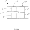
- Each current contact pair 14, 20 is arranged to be in a short circuit configuration, as shown in Figure 2a .
- the first and second current contacts 16, 18 of the first current contact pair 14 are in contact with one another (i.e. are touching one another) and the first and second current contacts 22, 24 of the second current contact pair 20 are in contact with one another (i.e. are touching one another).
- the first current contact 16, 22 in each current contact pair 14, 20 is arranged to be independently moveable relative to the corresponding second current contact 18, 24 and the second current contact 18, 24 in each current contact pair 14, 20 is arranged to be independently moveable relative to the corresponding first current contact 16,22.
- the first and second current contacts 16, 18, 22, 24 in each current contact pair 14, 20 are so moveable so that during initial insertion of the current transformer data acquisition board 12 into the current transformer connector 10 in use the first and second current contacts 16, 18, of the first current contact pair 14 are configured to separate from one another, in particular be urged away from one another, to permit breaking of the short circuit configuration of the first current contact pair 14 and making of an electrical connection between the first current contact pair 14 and the current transformer data acquisition board 12, while the second current contact pair 20 remains in the short circuit configuration.
- the first and second current contacts 16, 18, 22, 24 in each current contact pair 14, 20 are also so moveable so that during further insertion of the current transformer data acquisition board 12 into the current transformer connector 10 in use the first and second current contacts 22, 24 of the second current contact pair 20 are configured to separate from one another, in particular be urged away from one another, to permit breaking of the short circuit configuration of the second current contact pair 20. In this way, all the current contact pairs 14, 20 have broken their short circuit configuration and so the current contact pairs 14, 20 are in a "break" configuration, as shown in Figure 2c .
- the first and second current contacts 16, 18, 22, 24 are also independently moveable so that during initial removal of the current transformer data acquisition board 12 from the current transformer connector 10 in use the current contacts 22, 24 of the second current contact pair 16 are configured to return to the short circuit configuration while the first contact pair 14 remains in electrical connection with the current transformer data acquisition board 12 (as shown in Figure 2b ). Moreover, the first and second current contacts 16, 18 of the first current contact pair 14 are independently moveable so that during further removal of the current transformer data acquisition board 12 from the current transformer connector 10 in use the current contacts 16, 18 of the first current contact pair 14 are configured to return to the short circuit configuration (as shown in Figure 2a ).
- first and second current contacts 14, 16 of the first current contact pair 14 are biased towards one another and the first and second current contacts 22, 24 of the second current contact pair 20 are biased towards one another.
- the first and second current contacts 22, 24 of the second current contact pair 20 are also arranged to be independently moveable relative to one another so that the current contacts 22, 24 in the second current contact pair 20 make an electrical connection between the second current contact pair 20 and the current transformer data acquisition board 12 during further insertion of the current transformer data acquisition board 12. In this way, all of the current contact pairs 14, 20 are configured to make an electrical connection with the current transformer data acquisition board 12 in the "break" configuration (shown in Figure 2c ).
- only one of the first and second current contacts 16, 18, 22, 24 in each current contact pair 14, 20 may be independently moveable while the other current contact in that current contact pair is stationary.
- the first current contact 16 of the first current contact pair 14 may be moveable relative to a stationary second current contact 18 of the first current contact pair 14.
- only one of the first and second current contacts 14, 16, 22, 24 in each current contact pair 14, 20 may be biased towards to the other corresponding current contact.
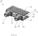
- the current transformer connector 10 further includes a current connector member 28 which supports the current contact pairs 14, 20.
- the first current connector member portion 30 supports the first current contacts 16, 22 of both the first and second current contact pairs 14, 20, while the second current connector member portion 32 supports the second current contacts 18, 24 of both the first and second current contact pairs 14, 20.
- first current contacts 16, 22 are formed from a single first current contact member 38 which includes seven fingers 40 to form the independently moveable first current contacts 16, 22.
- second current contacts 18, 24 are formed from a single second current contact member 42 which includes seven fingers 40 to form the independently moveable second current contacts 18, 24.
- the fingers 40 are formed such that the first and second current contact members 38, 42 are spring contacts.
- first current connector portion 30 and first current contact member 38 are described in more detail below with reference to Figure 3b . It will be understood that the features described apply mutatis mutandis to the second current connector portion 32 and the second current contact member 42.
- the first current contact member 38 includes a first contact portion 44 and a second contact portion 46.
- the first contact portion 44 is in contact with the first current connector member portion 30.
- the first contact portion 44 is secured, e.g. by a snap-fit arrangement, to the first current connector member portion 30.
- the first contact portion 44 is substantially flat so that it lies flat on top of a surface of the first current connector member portion 30.
- the first contact portion 44 may take any other form which permits it to be secured to the first current connector member portion 30.
- the second contact portion 46 extends from the first contact portion 44 to form the fingers 40.
- the second contact portion 46 is in contact with the first current member portion 30 and the second contact portion 46 of the second current contact member 42 (i.e. the second current contacts 18, 24 in the current contact pairs 14, 20).
- the second contact portion 46 has an arcuate profile, the crest 48 of which extends away from the first current connector member portion 30.
- the second contact portion 46 therefore extends from the first contact portion 44 (which is in contact with the first current member portion 30), away from the first current member portion 30 to reach the crest 48 of the arcuate profile, and back towards the first current member portion 30 to be in contact with the first current member portion 30.
- first and second current contact members 38, 42 may take another shape.
- the first and second contact members 38, 42 are formed from metal with the properties and/or dimensions to permit the fingers 40 to be independently moveable upon insertion of the current transformer data acquisition board 12.
- the first and second current contact member portions 30, 32 are formed separately from one another.
- the first and second current contact member portions 30, 32 are formed from separate pieces of metal, such as copper.
- the current terminals 34, 36 are tapped with M4 threads so that they are configured to accept M4 screws. This allows the current terminals 34, 36 to be able to receive external wiring from the current transformer.
- the current terminals 34, 36 are fixedly secured to a terminal portion 50 of the corresponding first and second current contact member portions 30, 32.
- the first and second current contact member portions 30, 32 are assembled together so that the crests 48 of the first and second current contact members 38, 42 touch and slightly compress the fingers 40, as shown in Figure 3a .
- Current is therefore able to flow from each current terminal 34, 36, through the corresponding current connector member portion 30, 32 and to the corresponding current contact member 38, 42.
- two or more of the current terminals 34, 36, the current connector member portions 30, 32 and/or the current contact members 38, 42 may be integrally formed with one another from a single piece of material (e.g. metal).
- a single piece of material e.g. metal
- the first current terminal 34 and the first current connector member portion 30 may be integrally formed from a single piece of metal
- the second current terminal 36 and the second current connector member portion 32 may be integrally formed from another single piece of metal.
- the current transformer connector 10 includes a first current aperture 52 which contains the first set 26 of contacts.
- the current transformer connector 10 is made from a plastic material.
- the current transformer connector 10 further includes second and third current apertures 54, 56 which each contain a corresponding second and third set 58, 60 of contacts.
- Each of the second and third sets 58, 60 includes current contact pairs 14, 20 as described hereinabove.
- Figure 1 shows only a portion of the current transformer connector 10, and so although not shown in Figure 1 , the current transformer connector 10 includes fourth, fifth and so on current apertures, each containing a corresponding set of contacts.
- the current transformer connector 10 may include a total of twelve current apertures, each containing corresponding current contact pairs.
- the apertures may include a mixture of current and voltage contact pairs, which is described in more detail below.
- Each of the first, second, third, and so on sets 26, 58, 60 of current contact pairs 14, 20 may be connected to a different phase of the electrical network or may instead be connected at different locations of the same phase of the electrical network.
- each set 26, 58, 60 of contacts has only one current aperture 52, 54, 56 (i.e. to form respective single current connections 62a, 62b, 62c)
- the current transformer connector 10 may include more than one current aperture 52, 54, 56 in each set 26, 58, 60.
- each row 26, 58, 60 of contacts shown in Figure 1 may include more than one aperture 52, 54, 56 and therefore create more than one current connection slot in each row 26, 58, 60.
- each set 26, 58, 60 of contacts would include multiple, e.g. three, current connections 62a, 62b, 62c.
- each set 26, 58, 60 of contacts includes a voltage aperture (not shown) containing a pair of voltage contacts, thus forming a voltage connection for connection to a voltage transformer.
- each set 26, 58, 60 of contacts includes a mixture of current and voltage connections.
- each set 26, 58, 60 of contacts may include two current connections 62a, 62b and one voltage connection or instead may include one current connection 62a and two voltage connections.
- a current transformer connection assembly according to the second embodiment of the invention is shown in Figures 4 and 5 and is designated generally by reference number 100.
- the current transformer connection assembly 100 includes a current transformer connector 102 which shares some of the same features as the current transformer connector 10 of the first embodiment, and like features share the same reference numeral.
- the current transformer connection assembly 100 further includes a first current transformer data acquisition board 104.
- the first current transformer data acquisition board 104 includes a first current channel member 106 that is arranged to be selectively inserted into the current transformer connector 102.
- the first current channel member 106 is arranged to be selectively inserted into the first current aperture 52 of the current transformer connector 102.
- the first current channel member 106 is shaped so that during initial insertion of the first current channel member 106 into the first current aperture 52 the current channel member 106 separates the current contacts 16, 18 of the first current contact pairs 14 from one another, in particular urges the current contacts 16, 18 away from one another, to break the short circuit configuration of the first current contact pairs 14 and make an electrical connection between the first current contact pairs 14 and the current channel member 106, while the second current contact pairs 20 remain in the short circuit configuration.
- the first current channel member 106 is further shaped so that during further insertion of the first current channel member 106 into the first current aperture 52 the first current channel member 106 separates the current contacts 22, 24 of the second current contact pairs 20 from one another, in particular urges the current contacts 22, 24 away from one another, to break the short circuit configuration of the second current contact pairs 20.
- the first current channel member 106 is also arranged to be selectively removed from the first current aperture 52 and, in such removing, the first current channel member 106 is shaped so that during initial removal the current contacts 22, 24 of the second current contact pairs 20 return to the short circuit configuration while the current contacts 16, 18 of the first current contact pairs 14 remain in electrical connection with the current channel member 106.
- the first current channel member 106 is also shaped so that during further removal of the first current channel member 106 from the first current aperture 54 the current contacts 16, 18 of the first current contact pairs 14 return to the short circuit configuration.
- the first current transformer data acquisition board 104 is described in more detail below with reference to Figure 5 .
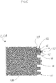
- the first current transformer data acquisition board 104 is in the form of a printed circuit board (PCB) 108, but in other embodiments it may take a different form.
- PCB printed circuit board
- the first current channel member 106 extends from an edge 109 of the PCB 108 and lies in the same plane as the PCB 108.
- the first current channel member 106 is symmetrical about the centre line 110 of the first current channel member 106.
- the first current channel member 106 includes first and second current channel member portions 112, 114.
- the first and second current channel member portions 112, 114 are positioned relative to one another so that the first current channel member portion 112 enters first into the current aperture 54 during initial insertion of the PCB 108 and so that the second current channel member portion 114 enters second into the current aperture 54 during further insertion of the PCB 108.
- the first current channel member portion 112 extends from the edge 109 of the PCB 108 by a first amount and the second current channel member portion 114 extends from the edge 109 of the PCB 108 by a second amount, the first amount being larger than the second amount. As such, the first current channel member portion 112 protrudes further from the edge 109 of the PCB 108 than the second current channel member portion 114.
- the second current channel member portion 114 extends from the edge 109 of the PCB 108 by a length L 1 and a width W 1 , while the first current channel member portion 112 extends from the second current channel member portion 114 by a length L 2 and a width W 2 .
- the length L 1 and width W 1 of the second current channel member portion 114 are larger than the length L 2 and width W 2 of the first current channel member portion 112.
- the first current channel member portion 112 extends at a centre portion 116 of the second current channel member portion 114, i.e. from a centre of the width W 1 of the second current channel member portion 114.
- the first current channel member portion 112 may instead extend from either side of the centre portion 116 of the second current channel member portion 114.
- the first current channel member 106 may include two first current channel member portions 112, each extending from either side of the centre portion 116 of the second current channel member portion 114.
- the first current channel member 106 includes current connection poles (not shown) on opposite faces of the PCB 108.
- the PCB 108 includes a second current channel member 118 spaced from the first current channel member 106.
- the second current channel member 118 is identical to the first current channel member 106.
- the PCB 108 further includes a voltage channel member 120 which is arranged to be inserted into a voltage aperture of the voltage transformer connector 102, as described in more detail below.
- the PCB 108 includes heavy copper outer layers (>1oz, for example) and local hard-gold plating in the areas where the first and second current contact pairs 14, 20 will come into contact with the PCB 108.
- the current transformer connector 102 differs from that of the first embodiment in that the first set 26 of contacts includes first and second current apertures 52, 54 and a voltage aperture 122.
- the first and second current aperture 52, 54 each include current contact pairs 14, 20 as described in relation to the first embodiment of the invention, thus forming respective current connections 62a, 62b.
- the voltage aperture 122 includes a pair of voltage contacts 124 (which are connectable to a voltage transformer), thus forming a voltage connection 126.
- the current transformer connector 102 further includes second and third sets 58, 60 of contacts, each set 58, 60 also including two current connections 62a, 62b and a single voltage connection 126.
- each set 26, 58, 60 of contacts may include only current connections 62a, 62b, 62c, or another ratio of current and voltage connections 62a, 62b, 62c, 126.
- the current transformer connection assembly 100 further includes second and third current transformer data acquisition boards 128, 130 each of which shares the same features as the first current transformer data acquisition board 104.
- the second current transformer data acquisition board 128 is arranged to be inserted into the second set 58 of contacts
- the third current transformer data acquisition board 130 is arranged to be inserted into the third set 60 of contacts.
- the current transformer data acquisition boards 104, 128, 130 are shaped to include current and voltage channel members 106, 120 required to insert into the corresponding combination of current and voltage apertures 52, 54, 56, 122 in a given set 26, 58, 60 of contacts.
- each of the current connections 62a, 62b is connected to a respective current transformer (not shown) of an electrical network via each current terminal 34, 36.
- the first and second current contact pairs 14, 20 are in the short circuit configuration so that current is able to flow through the current contact pairs 14, 20 via the first and second current connector member portions 30, 32.
- the current connections 62a, 62b may be connected to the same current transformer.
- the first current transformer data acquisition board 104 is inserted into the current transformer connector 102.
- the first and second current channel members 106, 118 are inserted into the first and second current apertures 52, 54 and the voltage channel member 120 is inserted into the voltage aperture 122.
- the first current channel member portion 112 upon initial insertion of the first current transformer data acquisition board 104, the first current channel member portion 112 enters the current aperture 52 first and pushes through the first current contact pairs 14, thus urging the first and second current contacts 16, 18 of the first current contact pairs 14 away from one another to break their short circuit configurations. Meanwhile, because of the extra length L 2 of the first current channel member portion 112 compared to the length of L 1 of the second current channel member portion 114, the second current contact pairs 20 remain in their short circuit configurations.
- first and second current contacts 16, 18 of the first current contact pairs 14 are biased towards one another, they are each deflected by the first current channel member portion 112 but continue to push towards one another. This means that the current contacts 16, 18 of the first current contact pairs 14 establish good contact with the first current transformer data acquisition board 104 so as to make an electrical connection with the first current transformer data acquisition board 104 (i.e. via the gold plating areas of the PCB 108).
- the second current channel member portion 114 enters further into the current aperture 52 and pushes through the second current contact pairs 20, thus urging the first and second current contacts 22, 24 of the second current contact pairs 20 away from one another to break their short circuit configurations. None of the current contact pairs 14, 20 is now in the short circuit configuration.
- first and second current contacts 22, 24 of the second current contact pairs 20 are biased towards one another, they are each deflected by the second current channel member portion 114 but continue to push towards one another. This means that the current contacts 22, 24 of the second current contact pairs 20 establish good contact with the first current transformer data acquisition board 104 so as to make an electrical connection with the first current transformer data acquisition board 104 (i.e. via the gold plating areas of the PCB 108).
- the voltage channel member 120 is inserted into the voltage aperture 122 so as to make electrical connection with the voltage contacts 124.
- the current transformer data acquisition board 104 includes current and voltage sensors (not shown) which are in turn connected to a protection relay (not shown).
- the current transformer data acquisition board 104 is pulled out from the current transformer connector 102.
- the second current channel member portion 114 is extracted first out of the current contact pairs 20 such that the first and second current contacts 22, 24 of the second current contact pairs 20 return back to their short circuit configuration via their biasing towards one another.
- the first current channel member portion 112 is then extracted out of the current contact pairs 14 such that the first and second current contacts 16, 18 of the first current contact pairs 14 return back to their short circuit configuration via their biasing towards one another.
- the current transformer data acquisition board 104 is therefore fully removed from the current transformer connector 102 and all of the current contact pairs 14, 20 are in their short circuit configuration.
Landscapes
- Physics & Mathematics (AREA)
- General Physics & Mathematics (AREA)
- Details Of Connecting Devices For Male And Female Coupling (AREA)
- Engineering & Computer Science (AREA)
- Power Engineering (AREA)
Priority Applications (3)
| Application Number | Priority Date | Filing Date | Title |
|---|---|---|---|
| EP17170468.7A EP3402001B1 (de) | 2017-05-10 | 2017-05-10 | Verbesserungen an oder im zusammenhang mit stromtransformaten |
| PCT/EP2018/060346 WO2018206284A1 (en) | 2017-05-10 | 2018-04-23 | Improvements in or relating to current transformers |
| US16/612,247 US11424584B2 (en) | 2017-05-10 | 2018-04-23 | Current transformer |
Applications Claiming Priority (1)
| Application Number | Priority Date | Filing Date | Title |
|---|---|---|---|
| EP17170468.7A EP3402001B1 (de) | 2017-05-10 | 2017-05-10 | Verbesserungen an oder im zusammenhang mit stromtransformaten |
Publications (2)
| Publication Number | Publication Date |
|---|---|
| EP3402001A1 true EP3402001A1 (de) | 2018-11-14 |
| EP3402001B1 EP3402001B1 (de) | 2021-02-17 |
Family
ID=58701487
Family Applications (1)
| Application Number | Title | Priority Date | Filing Date |
|---|---|---|---|
| EP17170468.7A Not-in-force EP3402001B1 (de) | 2017-05-10 | 2017-05-10 | Verbesserungen an oder im zusammenhang mit stromtransformaten |
Country Status (3)
| Country | Link |
|---|---|
| US (1) | US11424584B2 (de) |
| EP (1) | EP3402001B1 (de) |
| WO (1) | WO2018206284A1 (de) |
Citations (6)
| Publication number | Priority date | Publication date | Assignee | Title |
|---|---|---|---|---|
| JPH08240612A (ja) * | 1995-03-02 | 1996-09-17 | Hitachi Ltd | 差込式試験端子用プラグ |
| US5582519A (en) * | 1994-12-15 | 1996-12-10 | The Whitaker Corporation | Make-first-break-last ground connections |
| DE102010034863A1 (de) * | 2010-08-19 | 2012-02-23 | Phoenix Contact Gmbh & Co. Kg | Elektrische Anschlussklemme |
| EP2530794A1 (de) * | 2010-01-28 | 2012-12-05 | Sony Corporation | Steckverbinder und stromzufuhrsystem |
| US20140295680A1 (en) * | 2013-04-01 | 2014-10-02 | Tyco Electronics (Shanghai) Co., Ltd. | Electrical connector having an electrical contact with a plurality of contact beams |
| US20160291058A1 (en) * | 2014-10-12 | 2016-10-06 | Hubert Ostmeier | Safety test switch with actuation lever |
Family Cites Families (34)
| Publication number | Priority date | Publication date | Assignee | Title |
|---|---|---|---|---|
| NL142311B (nl) * | 1967-12-06 | 1974-05-15 | Amp Inc | Elektrisch verbindingsstelsel voor het verbinden van vaste elektrische geleiders met gedrukte elektrische geleiders op een paneel. |
| US4068915A (en) * | 1975-09-22 | 1978-01-17 | E. I. Du Pont De Nemours And Company | Electrical connector |
| US4070557A (en) * | 1976-07-26 | 1978-01-24 | Northern Telecom Limited | Apparatus for providing closed loop conditions in vacant module positions |
| US4087151A (en) * | 1976-07-28 | 1978-05-02 | Magnetic Controls Company | Printed circuit card edge connector with normalling contacts |
| US4106841A (en) * | 1977-03-11 | 1978-08-15 | Bunker Ramo Corporation | Electrical connector for printed circuit boards |
| US5162002A (en) * | 1990-03-30 | 1992-11-10 | Molex Incorporated | Card edge connector assembly |
| US5286215A (en) * | 1992-10-15 | 1994-02-15 | Adc Telecommunications, Inc. | Make-before-break PC board edge connector |
| US5893767A (en) * | 1997-05-30 | 1999-04-13 | The Whitaker Corporation | Electrical connector having a switch |
| JP3651216B2 (ja) * | 1997-12-15 | 2005-05-25 | 住友電装株式会社 | 分岐接続箱 |
| TW420419U (en) * | 1998-12-28 | 2001-01-21 | Hon Hai Prec Ind Co Ltd | Electrical connector |
| US6247948B1 (en) * | 1999-02-08 | 2001-06-19 | The Whitaker Corporation | Electrical connector and panel assembly |
| TW472964U (en) * | 2000-12-15 | 2002-01-11 | Hon Hai Prec Ind Co Ltd | Connector for electric card |
| RO121302B1 (ro) * | 2001-02-27 | 2007-02-28 | Mondragon Telecommunications S.L. | Ansamblu de conectare, pentru montarea şi conectarea filtrelor de bandă largă |
| US6488549B1 (en) * | 2001-06-06 | 2002-12-03 | Tyco Electronics Corporation | Electrical connector assembly with separate arcing zones |
| US20030054683A1 (en) * | 2001-08-14 | 2003-03-20 | Bryan Lyle S. | Arc prevention circuits |
| JP2003085122A (ja) * | 2001-09-13 | 2003-03-20 | Nec Corp | コンピュータシステムおよびスイッチコネクタ |
| US6764345B1 (en) * | 2003-05-27 | 2004-07-20 | Tyco Electronics Corporation | Electrical card edge connector with dual shorting contacts |
| US6863572B1 (en) * | 2003-08-19 | 2005-03-08 | Hon Hai Precision Ind. Co., Ltd. | Electrical connector with shock support |
| US6923655B2 (en) * | 2003-09-23 | 2005-08-02 | Hon Hai Precision Ind. Co., Ltd. | Electrical connector for interconnecting two intersected printed circuit boards |
| CN2770127Y (zh) * | 2004-12-14 | 2006-04-05 | 富士康(昆山)电脑接插件有限公司 | 电连接器 |
| US7172444B1 (en) * | 2005-07-28 | 2007-02-06 | Jui-Shu Huang | Hard drive contact pin connector device |
| JP4303259B2 (ja) * | 2006-05-15 | 2009-07-29 | 京セラエルコ株式会社 | コネクタ及びこのコネクタを備えた携帯端末 |
| JP4575962B2 (ja) * | 2008-01-25 | 2010-11-04 | 株式会社日本自動車部品総合研究所 | カードエッジコネクタ及びその組付方法 |
| JP5218074B2 (ja) * | 2008-04-28 | 2013-06-26 | 住友電装株式会社 | コネクタ |
| US8246358B2 (en) * | 2010-09-30 | 2012-08-21 | Rockwell Automation Technologies, Inc. | Contact device and method for insertion and removal of device under power without interruption |
| JP5979407B2 (ja) * | 2012-02-23 | 2016-08-24 | 第一精工株式会社 | スイッチ付同軸コネクタ |
| US8602801B2 (en) * | 2012-02-23 | 2013-12-10 | Hewlett-Packard Development Company, L.P. | Electrical jack |
| TWM455285U (zh) * | 2013-01-21 | 2013-06-11 | Insert Entpr Co Ltd | 超小型同軸微開關連接器 |
| US9004924B2 (en) * | 2013-03-08 | 2015-04-14 | SINGATRON TECHNOLOGY (HongKong) CO., LIMITED | Magnetic power connector and an electronic system using the magnetic power connector assembly |
| US9312652B2 (en) * | 2013-03-14 | 2016-04-12 | Tii Technologies Inc. | Switchable modular jack assembly for telecommunications systems |
| TWM480785U (zh) * | 2013-12-13 | 2014-06-21 | Advanced Connectek Inc | 插頭電連接器之切換裝置 |
| TWM497876U (zh) * | 2014-07-03 | 2015-03-21 | T Conn Prec Corp | 插座連接器之偵測結構 |
| US9941627B2 (en) * | 2015-09-30 | 2018-04-10 | Apple Inc. | Magnetic surface contacts |
| US9716333B1 (en) * | 2016-03-14 | 2017-07-25 | Amphenol East Asia Electronic Technology (Shen Zhen) Co., Ltd. | Heavy current female connector |
-
2017
- 2017-05-10 EP EP17170468.7A patent/EP3402001B1/de not_active Not-in-force
-
2018
- 2018-04-23 US US16/612,247 patent/US11424584B2/en active Active
- 2018-04-23 WO PCT/EP2018/060346 patent/WO2018206284A1/en not_active Ceased
Patent Citations (6)
| Publication number | Priority date | Publication date | Assignee | Title |
|---|---|---|---|---|
| US5582519A (en) * | 1994-12-15 | 1996-12-10 | The Whitaker Corporation | Make-first-break-last ground connections |
| JPH08240612A (ja) * | 1995-03-02 | 1996-09-17 | Hitachi Ltd | 差込式試験端子用プラグ |
| EP2530794A1 (de) * | 2010-01-28 | 2012-12-05 | Sony Corporation | Steckverbinder und stromzufuhrsystem |
| DE102010034863A1 (de) * | 2010-08-19 | 2012-02-23 | Phoenix Contact Gmbh & Co. Kg | Elektrische Anschlussklemme |
| US20140295680A1 (en) * | 2013-04-01 | 2014-10-02 | Tyco Electronics (Shanghai) Co., Ltd. | Electrical connector having an electrical contact with a plurality of contact beams |
| US20160291058A1 (en) * | 2014-10-12 | 2016-10-06 | Hubert Ostmeier | Safety test switch with actuation lever |
Also Published As
| Publication number | Publication date |
|---|---|
| EP3402001B1 (de) | 2021-02-17 |
| WO2018206284A1 (en) | 2018-11-15 |
| US20200176975A1 (en) | 2020-06-04 |
| US11424584B2 (en) | 2022-08-23 |
Similar Documents
| Publication | Publication Date | Title |
|---|---|---|
| DE4333263C2 (de) | Reihenklemme | |
| KR100846886B1 (ko) | 스프링식 플러그 단자 | |
| US7566234B2 (en) | Connector apparatus with code means | |
| US7713083B1 (en) | Jumper device for controlling connection of pins of electrical device on mainboard | |
| US7168977B2 (en) | Plug-in jumper for electrical junction and/or connecting terminals and electrical junction and/or connecting terminal | |
| EP3111515B1 (de) | Reihenklemme und reihenklemmenblock | |
| DE102010010260C5 (de) | Steckverbinder | |
| US7465184B2 (en) | Connector assembly including insulation displacement elements configured for attachment to a printed circuit | |
| CN104638405A (zh) | 电连接器 | |
| WO2008055746A3 (de) | Elektrisches anschlusselement | |
| EP2894724A1 (de) | Anschlussklemme | |
| US9300066B2 (en) | High-voltage resistance and retention of printed flex circuits | |
| DE102014103059B4 (de) | Reihenklemmenanordnung | |
| US9941613B2 (en) | Electrical connector for a bus bar | |
| US8262404B2 (en) | Terminal block and contact element for telecommunications and data systems | |
| US20070064373A1 (en) | Overvoltage protection magazine for a device of telecommunications technology | |
| US20160093959A1 (en) | Plug-in bridge having plate elements lying one over the other | |
| WO2015004058A1 (de) | Leiterplattenverbinder | |
| US20170271830A1 (en) | Connecting adapter for a connecting terminal assembly | |
| US11424584B2 (en) | Current transformer | |
| DE10030954A1 (de) | Stromverteiler | |
| AU748833B2 (en) | Protective connector for a telecommunications device | |
| US12184006B2 (en) | Conductor connection terminal having first and second housings with electrically joined busbars | |
| US20120033339A1 (en) | Surge protection magazine for a device in telecommunications and data technology | |
| DE102011083921B4 (de) | Schutzschaltgerät |
Legal Events
| Date | Code | Title | Description |
|---|---|---|---|
| PUAI | Public reference made under article 153(3) epc to a published international application that has entered the european phase |
Free format text: ORIGINAL CODE: 0009012 |
|
| STAA | Information on the status of an ep patent application or granted ep patent |
Free format text: STATUS: THE APPLICATION HAS BEEN PUBLISHED |
|
| AK | Designated contracting states |
Kind code of ref document: A1 Designated state(s): AL AT BE BG CH CY CZ DE DK EE ES FI FR GB GR HR HU IE IS IT LI LT LU LV MC MK MT NL NO PL PT RO RS SE SI SK SM TR |
|
| AX | Request for extension of the european patent |
Extension state: BA ME |
|
| STAA | Information on the status of an ep patent application or granted ep patent |
Free format text: STATUS: REQUEST FOR EXAMINATION WAS MADE |
|
| 17P | Request for examination filed |
Effective date: 20190514 |
|
| RBV | Designated contracting states (corrected) |
Designated state(s): AL AT BE BG CH CY CZ DE DK EE ES FI FR GB GR HR HU IE IS IT LI LT LU LV MC MK MT NL NO PL PT RO RS SE SI SK SM TR |
|
| GRAP | Despatch of communication of intention to grant a patent |
Free format text: ORIGINAL CODE: EPIDOSNIGR1 |
|
| STAA | Information on the status of an ep patent application or granted ep patent |
Free format text: STATUS: GRANT OF PATENT IS INTENDED |
|
| INTG | Intention to grant announced |
Effective date: 20200910 |
|
| GRAS | Grant fee paid |
Free format text: ORIGINAL CODE: EPIDOSNIGR3 |
|
| GRAA | (expected) grant |
Free format text: ORIGINAL CODE: 0009210 |
|
| STAA | Information on the status of an ep patent application or granted ep patent |
Free format text: STATUS: THE PATENT HAS BEEN GRANTED |
|
| AK | Designated contracting states |
Kind code of ref document: B1 Designated state(s): AL AT BE BG CH CY CZ DE DK EE ES FI FR GB GR HR HU IE IS IT LI LT LU LV MC MK MT NL NO PL PT RO RS SE SI SK SM TR |
|
| REG | Reference to a national code |
Ref country code: GB Ref legal event code: FG4D |
|
| REG | Reference to a national code |
Ref country code: CH Ref legal event code: EP |
|
| REG | Reference to a national code |
Ref country code: DE Ref legal event code: R096 Ref document number: 602017032505 Country of ref document: DE |
|
| REG | Reference to a national code |
Ref country code: AT Ref legal event code: REF Ref document number: 1362699 Country of ref document: AT Kind code of ref document: T Effective date: 20210315 |
|
| REG | Reference to a national code |
Ref country code: IE Ref legal event code: FG4D |
|
| REG | Reference to a national code |
Ref country code: SE Ref legal event code: TRGR |
|
| REG | Reference to a national code |
Ref country code: LT Ref legal event code: MG9D |
|
| REG | Reference to a national code |
Ref country code: NL Ref legal event code: MP Effective date: 20210217 |
|
| PG25 | Lapsed in a contracting state [announced via postgrant information from national office to epo] |
Ref country code: LT Free format text: LAPSE BECAUSE OF FAILURE TO SUBMIT A TRANSLATION OF THE DESCRIPTION OR TO PAY THE FEE WITHIN THE PRESCRIBED TIME-LIMIT Effective date: 20210217 Ref country code: BG Free format text: LAPSE BECAUSE OF FAILURE TO SUBMIT A TRANSLATION OF THE DESCRIPTION OR TO PAY THE FEE WITHIN THE PRESCRIBED TIME-LIMIT Effective date: 20210517 Ref country code: PT Free format text: LAPSE BECAUSE OF FAILURE TO SUBMIT A TRANSLATION OF THE DESCRIPTION OR TO PAY THE FEE WITHIN THE PRESCRIBED TIME-LIMIT Effective date: 20210617 Ref country code: NO Free format text: LAPSE BECAUSE OF FAILURE TO SUBMIT A TRANSLATION OF THE DESCRIPTION OR TO PAY THE FEE WITHIN THE PRESCRIBED TIME-LIMIT Effective date: 20210517 Ref country code: FI Free format text: LAPSE BECAUSE OF FAILURE TO SUBMIT A TRANSLATION OF THE DESCRIPTION OR TO PAY THE FEE WITHIN THE PRESCRIBED TIME-LIMIT Effective date: 20210217 Ref country code: HR Free format text: LAPSE BECAUSE OF FAILURE TO SUBMIT A TRANSLATION OF THE DESCRIPTION OR TO PAY THE FEE WITHIN THE PRESCRIBED TIME-LIMIT Effective date: 20210217 Ref country code: GR Free format text: LAPSE BECAUSE OF FAILURE TO SUBMIT A TRANSLATION OF THE DESCRIPTION OR TO PAY THE FEE WITHIN THE PRESCRIBED TIME-LIMIT Effective date: 20210518 |
|
| REG | Reference to a national code |
Ref country code: AT Ref legal event code: MK05 Ref document number: 1362699 Country of ref document: AT Kind code of ref document: T Effective date: 20210217 |
|
| PG25 | Lapsed in a contracting state [announced via postgrant information from national office to epo] |
Ref country code: PL Free format text: LAPSE BECAUSE OF FAILURE TO SUBMIT A TRANSLATION OF THE DESCRIPTION OR TO PAY THE FEE WITHIN THE PRESCRIBED TIME-LIMIT Effective date: 20210217 Ref country code: NL Free format text: LAPSE BECAUSE OF FAILURE TO SUBMIT A TRANSLATION OF THE DESCRIPTION OR TO PAY THE FEE WITHIN THE PRESCRIBED TIME-LIMIT Effective date: 20210217 Ref country code: RS Free format text: LAPSE BECAUSE OF FAILURE TO SUBMIT A TRANSLATION OF THE DESCRIPTION OR TO PAY THE FEE WITHIN THE PRESCRIBED TIME-LIMIT Effective date: 20210217 Ref country code: LV Free format text: LAPSE BECAUSE OF FAILURE TO SUBMIT A TRANSLATION OF THE DESCRIPTION OR TO PAY THE FEE WITHIN THE PRESCRIBED TIME-LIMIT Effective date: 20210217 |
|
| PG25 | Lapsed in a contracting state [announced via postgrant information from national office to epo] |
Ref country code: IS Free format text: LAPSE BECAUSE OF FAILURE TO SUBMIT A TRANSLATION OF THE DESCRIPTION OR TO PAY THE FEE WITHIN THE PRESCRIBED TIME-LIMIT Effective date: 20210617 |
|
| PG25 | Lapsed in a contracting state [announced via postgrant information from national office to epo] |
Ref country code: EE Free format text: LAPSE BECAUSE OF FAILURE TO SUBMIT A TRANSLATION OF THE DESCRIPTION OR TO PAY THE FEE WITHIN THE PRESCRIBED TIME-LIMIT Effective date: 20210217 Ref country code: CZ Free format text: LAPSE BECAUSE OF FAILURE TO SUBMIT A TRANSLATION OF THE DESCRIPTION OR TO PAY THE FEE WITHIN THE PRESCRIBED TIME-LIMIT Effective date: 20210217 Ref country code: AT Free format text: LAPSE BECAUSE OF FAILURE TO SUBMIT A TRANSLATION OF THE DESCRIPTION OR TO PAY THE FEE WITHIN THE PRESCRIBED TIME-LIMIT Effective date: 20210217 Ref country code: SM Free format text: LAPSE BECAUSE OF FAILURE TO SUBMIT A TRANSLATION OF THE DESCRIPTION OR TO PAY THE FEE WITHIN THE PRESCRIBED TIME-LIMIT Effective date: 20210217 |
|
| REG | Reference to a national code |
Ref country code: DE Ref legal event code: R097 Ref document number: 602017032505 Country of ref document: DE |
|
| PG25 | Lapsed in a contracting state [announced via postgrant information from national office to epo] |
Ref country code: DK Free format text: LAPSE BECAUSE OF FAILURE TO SUBMIT A TRANSLATION OF THE DESCRIPTION OR TO PAY THE FEE WITHIN THE PRESCRIBED TIME-LIMIT Effective date: 20210217 Ref country code: RO Free format text: LAPSE BECAUSE OF FAILURE TO SUBMIT A TRANSLATION OF THE DESCRIPTION OR TO PAY THE FEE WITHIN THE PRESCRIBED TIME-LIMIT Effective date: 20210217 Ref country code: SK Free format text: LAPSE BECAUSE OF FAILURE TO SUBMIT A TRANSLATION OF THE DESCRIPTION OR TO PAY THE FEE WITHIN THE PRESCRIBED TIME-LIMIT Effective date: 20210217 |
|
| REG | Reference to a national code |
Ref country code: DE Ref legal event code: R119 Ref document number: 602017032505 Country of ref document: DE |
|
| PLBE | No opposition filed within time limit |
Free format text: ORIGINAL CODE: 0009261 |
|
| STAA | Information on the status of an ep patent application or granted ep patent |
Free format text: STATUS: NO OPPOSITION FILED WITHIN TIME LIMIT |
|
| REG | Reference to a national code |
Ref country code: SE Ref legal event code: EUG |
|
| REG | Reference to a national code |
Ref country code: CH Ref legal event code: PL |
|
| 26N | No opposition filed |
Effective date: 20211118 |
|
| GBPC | Gb: european patent ceased through non-payment of renewal fee |
Effective date: 20210517 |
|
| PG25 | Lapsed in a contracting state [announced via postgrant information from national office to epo] |
Ref country code: LI Free format text: LAPSE BECAUSE OF NON-PAYMENT OF DUE FEES Effective date: 20210531 Ref country code: LU Free format text: LAPSE BECAUSE OF NON-PAYMENT OF DUE FEES Effective date: 20210510 Ref country code: MC Free format text: LAPSE BECAUSE OF FAILURE TO SUBMIT A TRANSLATION OF THE DESCRIPTION OR TO PAY THE FEE WITHIN THE PRESCRIBED TIME-LIMIT Effective date: 20210217 Ref country code: CH Free format text: LAPSE BECAUSE OF NON-PAYMENT OF DUE FEES Effective date: 20210531 Ref country code: AL Free format text: LAPSE BECAUSE OF FAILURE TO SUBMIT A TRANSLATION OF THE DESCRIPTION OR TO PAY THE FEE WITHIN THE PRESCRIBED TIME-LIMIT Effective date: 20210217 Ref country code: ES Free format text: LAPSE BECAUSE OF FAILURE TO SUBMIT A TRANSLATION OF THE DESCRIPTION OR TO PAY THE FEE WITHIN THE PRESCRIBED TIME-LIMIT Effective date: 20210217 Ref country code: SE Free format text: LAPSE BECAUSE OF NON-PAYMENT OF DUE FEES Effective date: 20210511 |
|
| REG | Reference to a national code |
Ref country code: BE Ref legal event code: MM Effective date: 20210531 |
|
| PG25 | Lapsed in a contracting state [announced via postgrant information from national office to epo] |
Ref country code: SI Free format text: LAPSE BECAUSE OF FAILURE TO SUBMIT A TRANSLATION OF THE DESCRIPTION OR TO PAY THE FEE WITHIN THE PRESCRIBED TIME-LIMIT Effective date: 20210217 |
|
| PG25 | Lapsed in a contracting state [announced via postgrant information from national office to epo] |
Ref country code: IT Free format text: LAPSE BECAUSE OF FAILURE TO SUBMIT A TRANSLATION OF THE DESCRIPTION OR TO PAY THE FEE WITHIN THE PRESCRIBED TIME-LIMIT Effective date: 20210217 Ref country code: IE Free format text: LAPSE BECAUSE OF NON-PAYMENT OF DUE FEES Effective date: 20210510 Ref country code: GB Free format text: LAPSE BECAUSE OF NON-PAYMENT OF DUE FEES Effective date: 20210517 Ref country code: DE Free format text: LAPSE BECAUSE OF NON-PAYMENT OF DUE FEES Effective date: 20211201 |
|
| PG25 | Lapsed in a contracting state [announced via postgrant information from national office to epo] |
Ref country code: IS Free format text: LAPSE BECAUSE OF FAILURE TO SUBMIT A TRANSLATION OF THE DESCRIPTION OR TO PAY THE FEE WITHIN THE PRESCRIBED TIME-LIMIT Effective date: 20210617 Ref country code: FR Free format text: LAPSE BECAUSE OF NON-PAYMENT OF DUE FEES Effective date: 20210531 |
|
| PG25 | Lapsed in a contracting state [announced via postgrant information from national office to epo] |
Ref country code: BE Free format text: LAPSE BECAUSE OF NON-PAYMENT OF DUE FEES Effective date: 20210531 |
|
| PG25 | Lapsed in a contracting state [announced via postgrant information from national office to epo] |
Ref country code: CY Free format text: LAPSE BECAUSE OF FAILURE TO SUBMIT A TRANSLATION OF THE DESCRIPTION OR TO PAY THE FEE WITHIN THE PRESCRIBED TIME-LIMIT Effective date: 20210217 |
|
| PG25 | Lapsed in a contracting state [announced via postgrant information from national office to epo] |
Ref country code: HU Free format text: LAPSE BECAUSE OF FAILURE TO SUBMIT A TRANSLATION OF THE DESCRIPTION OR TO PAY THE FEE WITHIN THE PRESCRIBED TIME-LIMIT; INVALID AB INITIO Effective date: 20170510 |
|
| PG25 | Lapsed in a contracting state [announced via postgrant information from national office to epo] |
Ref country code: MK Free format text: LAPSE BECAUSE OF FAILURE TO SUBMIT A TRANSLATION OF THE DESCRIPTION OR TO PAY THE FEE WITHIN THE PRESCRIBED TIME-LIMIT Effective date: 20210217 |
|
| PG25 | Lapsed in a contracting state [announced via postgrant information from national office to epo] |
Ref country code: TR Free format text: LAPSE BECAUSE OF FAILURE TO SUBMIT A TRANSLATION OF THE DESCRIPTION OR TO PAY THE FEE WITHIN THE PRESCRIBED TIME-LIMIT Effective date: 20210217 |
|
| PG25 | Lapsed in a contracting state [announced via postgrant information from national office to epo] |
Ref country code: MT Free format text: LAPSE BECAUSE OF FAILURE TO SUBMIT A TRANSLATION OF THE DESCRIPTION OR TO PAY THE FEE WITHIN THE PRESCRIBED TIME-LIMIT Effective date: 20210217 |