EP3401848A1 - Quantum device with spin qubits - Google Patents
Quantum device with spin qubits Download PDFInfo
- Publication number
- EP3401848A1 EP3401848A1 EP18171613.5A EP18171613A EP3401848A1 EP 3401848 A1 EP3401848 A1 EP 3401848A1 EP 18171613 A EP18171613 A EP 18171613A EP 3401848 A1 EP3401848 A1 EP 3401848A1
- Authority
- EP
- European Patent Office
- Prior art keywords
- qubits
- portions
- semiconductor
- electrically conductive
- quantum device
- Prior art date
- Legal status (The legal status is an assumption and is not a legal conclusion. Google has not performed a legal analysis and makes no representation as to the accuracy of the status listed.)
- Granted
Links
- 239000004065 semiconductor Substances 0.000 claims abstract description 126
- 230000004888 barrier function Effects 0.000 claims abstract description 92
- 239000011159 matrix material Substances 0.000 claims abstract description 75
- 238000005259 measurement Methods 0.000 claims abstract description 67
- 239000002096 quantum dot Substances 0.000 claims abstract description 60
- 238000001465 metallisation Methods 0.000 claims abstract description 20
- 230000005669 field effect Effects 0.000 claims abstract description 7
- 239000002800 charge carrier Substances 0.000 claims description 15
- 239000004020 conductor Substances 0.000 claims description 13
- 230000008878 coupling Effects 0.000 claims description 7
- 238000010168 coupling process Methods 0.000 claims description 7
- 238000005859 coupling reaction Methods 0.000 claims description 7
- 238000004519 manufacturing process Methods 0.000 claims description 5
- 239000010410 layer Substances 0.000 description 93
- 239000003989 dielectric material Substances 0.000 description 20
- 229910004298 SiO 2 Inorganic materials 0.000 description 9
- 238000001514 detection method Methods 0.000 description 8
- 238000005530 etching Methods 0.000 description 8
- 239000000463 material Substances 0.000 description 6
- 238000000151 deposition Methods 0.000 description 5
- 229910052710 silicon Inorganic materials 0.000 description 5
- 239000010703 silicon Substances 0.000 description 5
- 230000008021 deposition Effects 0.000 description 4
- 150000004767 nitrides Chemical class 0.000 description 4
- 238000005421 electrostatic potential Methods 0.000 description 3
- 229910021420 polycrystalline silicon Inorganic materials 0.000 description 3
- 239000011248 coating agent Substances 0.000 description 2
- 238000000576 coating method Methods 0.000 description 2
- 229910052751 metal Inorganic materials 0.000 description 2
- 239000002184 metal Substances 0.000 description 2
- 229920003209 poly(hydridosilsesquioxane) Polymers 0.000 description 2
- 229920005591 polysilicon Polymers 0.000 description 2
- 238000011176 pooling Methods 0.000 description 2
- 239000007787 solid Substances 0.000 description 2
- 239000000758 substrate Substances 0.000 description 2
- 230000005428 wave function Effects 0.000 description 2
- 229910052581 Si3N4 Inorganic materials 0.000 description 1
- VYPSYNLAJGMNEJ-UHFFFAOYSA-N Silicium dioxide Chemical compound O=[Si]=O VYPSYNLAJGMNEJ-UHFFFAOYSA-N 0.000 description 1
- 241001080024 Telles Species 0.000 description 1
- ATJFFYVFTNAWJD-UHFFFAOYSA-N Tin Chemical compound [Sn] ATJFFYVFTNAWJD-UHFFFAOYSA-N 0.000 description 1
- 238000004364 calculation method Methods 0.000 description 1
- 238000004140 cleaning Methods 0.000 description 1
- 238000012937 correction Methods 0.000 description 1
- 238000010292 electrical insulation Methods 0.000 description 1
- 238000000407 epitaxy Methods 0.000 description 1
- 230000002209 hydrophobic effect Effects 0.000 description 1
- 238000012423 maintenance Methods 0.000 description 1
- 238000005457 optimization Methods 0.000 description 1
- 238000012545 processing Methods 0.000 description 1
- HQVNEWCFYHHQES-UHFFFAOYSA-N silicon nitride Chemical compound N12[Si]34N5[Si]62N3[Si]51N64 HQVNEWCFYHHQES-UHFFFAOYSA-N 0.000 description 1
- 229910052814 silicon oxide Inorganic materials 0.000 description 1
- 239000002344 surface layer Substances 0.000 description 1
- WFKWXMTUELFFGS-UHFFFAOYSA-N tungsten Chemical compound [W] WFKWXMTUELFFGS-UHFFFAOYSA-N 0.000 description 1
- 229910052721 tungsten Inorganic materials 0.000 description 1
- 239000010937 tungsten Substances 0.000 description 1
- 230000005641 tunneling Effects 0.000 description 1
Images


Classifications
-
- H—ELECTRICITY
- H10—SEMICONDUCTOR DEVICES; ELECTRIC SOLID-STATE DEVICES NOT OTHERWISE PROVIDED FOR
- H10B—ELECTRONIC MEMORY DEVICES
- H10B99/00—Subject matter not provided for in other groups of this subclass
-
- H—ELECTRICITY
- H01—ELECTRIC ELEMENTS
- H01L—SEMICONDUCTOR DEVICES NOT COVERED BY CLASS H10
- H01L29/00—Semiconductor devices adapted for rectifying, amplifying, oscillating or switching, or capacitors or resistors with at least one potential-jump barrier or surface barrier, e.g. PN junction depletion layer or carrier concentration layer; Details of semiconductor bodies or of electrodes thereof ; Multistep manufacturing processes therefor
- H01L29/66—Types of semiconductor device ; Multistep manufacturing processes therefor
- H01L29/66977—Quantum effect devices, e.g. using quantum reflection, diffraction or interference effects, i.e. Bragg- or Aharonov-Bohm effects
-
- G—PHYSICS
- G06—COMPUTING; CALCULATING OR COUNTING
- G06N—COMPUTING ARRANGEMENTS BASED ON SPECIFIC COMPUTATIONAL MODELS
- G06N10/00—Quantum computing, i.e. information processing based on quantum-mechanical phenomena
-
- H—ELECTRICITY
- H01—ELECTRIC ELEMENTS
- H01L—SEMICONDUCTOR DEVICES NOT COVERED BY CLASS H10
- H01L23/00—Details of semiconductor or other solid state devices
- H01L23/52—Arrangements for conducting electric current within the device in operation from one component to another, i.e. interconnections, e.g. wires, lead frames
- H01L23/522—Arrangements for conducting electric current within the device in operation from one component to another, i.e. interconnections, e.g. wires, lead frames including external interconnections consisting of a multilayer structure of conductive and insulating layers inseparably formed on the semiconductor body
- H01L23/5226—Via connections in a multilevel interconnection structure
-
- H—ELECTRICITY
- H01—ELECTRIC ELEMENTS
- H01L—SEMICONDUCTOR DEVICES NOT COVERED BY CLASS H10
- H01L29/00—Semiconductor devices adapted for rectifying, amplifying, oscillating or switching, or capacitors or resistors with at least one potential-jump barrier or surface barrier, e.g. PN junction depletion layer or carrier concentration layer; Details of semiconductor bodies or of electrodes thereof ; Multistep manufacturing processes therefor
- H01L29/40—Electrodes ; Multistep manufacturing processes therefor
- H01L29/41—Electrodes ; Multistep manufacturing processes therefor characterised by their shape, relative sizes or dispositions
- H01L29/423—Electrodes ; Multistep manufacturing processes therefor characterised by their shape, relative sizes or dispositions not carrying the current to be rectified, amplified or switched
-
- H—ELECTRICITY
- H01—ELECTRIC ELEMENTS
- H01L—SEMICONDUCTOR DEVICES NOT COVERED BY CLASS H10
- H01L29/00—Semiconductor devices adapted for rectifying, amplifying, oscillating or switching, or capacitors or resistors with at least one potential-jump barrier or surface barrier, e.g. PN junction depletion layer or carrier concentration layer; Details of semiconductor bodies or of electrodes thereof ; Multistep manufacturing processes therefor
- H01L29/66—Types of semiconductor device ; Multistep manufacturing processes therefor
- H01L29/66984—Devices using spin polarized carriers
-
- B—PERFORMING OPERATIONS; TRANSPORTING
- B82—NANOTECHNOLOGY
- B82Y—SPECIFIC USES OR APPLICATIONS OF NANOSTRUCTURES; MEASUREMENT OR ANALYSIS OF NANOSTRUCTURES; MANUFACTURE OR TREATMENT OF NANOSTRUCTURES
- B82Y10/00—Nanotechnology for information processing, storage or transmission, e.g. quantum computing or single electron logic
-
- H—ELECTRICITY
- H01—ELECTRIC ELEMENTS
- H01L—SEMICONDUCTOR DEVICES NOT COVERED BY CLASS H10
- H01L29/00—Semiconductor devices adapted for rectifying, amplifying, oscillating or switching, or capacitors or resistors with at least one potential-jump barrier or surface barrier, e.g. PN junction depletion layer or carrier concentration layer; Details of semiconductor bodies or of electrodes thereof ; Multistep manufacturing processes therefor
- H01L29/66—Types of semiconductor device ; Multistep manufacturing processes therefor
- H01L29/68—Types of semiconductor device ; Multistep manufacturing processes therefor controllable by only the electric current supplied, or only the electric potential applied, to an electrode which does not carry the current to be rectified, amplified or switched
- H01L29/76—Unipolar devices, e.g. field effect transistors
- H01L29/7606—Transistor-like structures, e.g. hot electron transistor [HET]; metal base transistor [MBT]
-
- H—ELECTRICITY
- H01—ELECTRIC ELEMENTS
- H01L—SEMICONDUCTOR DEVICES NOT COVERED BY CLASS H10
- H01L29/00—Semiconductor devices adapted for rectifying, amplifying, oscillating or switching, or capacitors or resistors with at least one potential-jump barrier or surface barrier, e.g. PN junction depletion layer or carrier concentration layer; Details of semiconductor bodies or of electrodes thereof ; Multistep manufacturing processes therefor
- H01L29/66—Types of semiconductor device ; Multistep manufacturing processes therefor
- H01L29/68—Types of semiconductor device ; Multistep manufacturing processes therefor controllable by only the electric current supplied, or only the electric potential applied, to an electrode which does not carry the current to be rectified, amplified or switched
- H01L29/76—Unipolar devices, e.g. field effect transistors
- H01L29/772—Field effect transistors
- H01L29/78—Field effect transistors with field effect produced by an insulated gate
- H01L29/786—Thin film transistors, i.e. transistors with a channel being at least partly a thin film
- H01L29/78642—Vertical transistors
-
- H—ELECTRICITY
- H01—ELECTRIC ELEMENTS
- H01L—SEMICONDUCTOR DEVICES NOT COVERED BY CLASS H10
- H01L29/00—Semiconductor devices adapted for rectifying, amplifying, oscillating or switching, or capacitors or resistors with at least one potential-jump barrier or surface barrier, e.g. PN junction depletion layer or carrier concentration layer; Details of semiconductor bodies or of electrodes thereof ; Multistep manufacturing processes therefor
- H01L29/66—Types of semiconductor device ; Multistep manufacturing processes therefor
- H01L29/68—Types of semiconductor device ; Multistep manufacturing processes therefor controllable by only the electric current supplied, or only the electric potential applied, to an electrode which does not carry the current to be rectified, amplified or switched
- H01L29/76—Unipolar devices, e.g. field effect transistors
- H01L29/772—Field effect transistors
- H01L29/78—Field effect transistors with field effect produced by an insulated gate
- H01L29/786—Thin film transistors, i.e. transistors with a channel being at least partly a thin film
- H01L29/78645—Thin film transistors, i.e. transistors with a channel being at least partly a thin film with multiple gate
Definitions
- the invention relates to the field of processing quantum information, or quantum computing.
- the invention particularly relates to a quantum-bit quantum device (called quantum bit) or spin qubit.
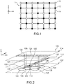
- qubit matrices are produced, for example from silicon, in the form of a two-dimensional matrix 1 as represented in FIG. figure 1 .
- the blanks referenced 10 represent data qubits and the black circles referenced 12 represent qubits of measurement.
- the qubits 10, 12 neighbors are interconnected to each other by tunnel barriers 14.
- the data qubits 10 are arranged in staggered relation to each other, and the measurement qubits 12 are arranged in staggered rows. one against another.
- These qubits 10, 12 are aligned and arranged forming rows and columns.
- each data qubit 10 is connected to two (for a data qubit 10 located in one corner of the matrix), three (for a data qubit 10 being on one edge of the matrix) or four (for all other data qubits 10 not in a corner or on an edge of the matrix) measurement qubits 12, and that each measurement qubit 12 is connected to two (for a qubit 12 in one corner of the array), three (for a measurement qubit 12 on one edge of the array) or four (for all other measurement qubits 12 not in a corner or on an edge of the matrix) data qubits 10.
- each of the measurement qubits 12 must be coupled to a detection element (not shown on the figure 1 ) whose operation is comparable to that of a single electron transistor or "Single Electron Transistor" (SET), for detecting whether a charge is present or not on the qubit at which the detection element is coupled.
- This detection element must also be able to be used to send or receive a charge carrier (electron or hole) from or to at least one of the measurement qubit 12 (and if possible also on at least one of the data qubits 10).
- a first problem which arises with such a matrix 1 of qubits concerns the addressing of the qubits 10, 12 which must be realized in such a structure. Indeed, each of the measurement qubits 12, and possibly each of the data qubits 10, must be connected to an electrical connection forming an electrical access to this qubit from outside the matrix 1.
- the realization of electrical addressing connections to each of these nine qubits requires at least two levels of electrical interconnections: a first level for the central qubit of this matrix and a second level for the other qubits around this central qubit.
- a second problem posed by such a matrix 1 relates to the realization of the detection elements to be coupled to the qubits. Indeed, given the dimensions sought for the realization of qubits (two neighboring qubits being for example spaced from each other by a distance between about 5 nm and 100 nm, and each qubit has lateral dimensions, for example example a diameter, included between about 5 nm and 100 nm), the realization of these detection elements within this matrix 1 of qubits is hardly possible.
- a third problem posed by such a matrix 1 is that as for carrying out the qubit addressing, performing the addressing of the detection elements is problematic because of the large number of electrical connections to be made.
- An object of the present invention is to provide a quantum quantum spin device in which the addressing of qubits arranged forming a two-dimensional matrix is performed with a reduced number of levels of electrical interconnections.
- the control of an individual qubit can come from the in-line and column addressing of the tunnel barriers (for example two, three or four depending on the arrangement of the qubit addressed within the matrix) connected to this qubit and controlled by the electrostatic grids formed opposite these tunnel barriers.
- the tunnel barriers may be formed by semiconductor portions narrower than those forming the qubits. Such narrower semiconductor portions are called "constrictions”.
- Each qubit of data can be connected to at least two neighboring measurement qubits and each measurement qubit can be connected to at least two neighboring data qubits.
- Each of the first electrically conductive portions may be connected to the first ends of the first conductive vias whose second ends are arranged opposite the first tunnel barriers connecting data qubits and measurement qubits arranged on two adjacent columns of the first matrix, and each second electrically conductive portions may be connected to the first ends of the second conductive vias whose second ends are arranged opposite the second tunnel barriers connecting data qubits and measuring qubits arranged on two adjacent lines of the first matrix.
- the quantum device may further comprise a second semiconductor layer comprising a second matrix of charge detectors, each comprising for example a quantum dot (or quantum dot), each of the measurement qubits.
- a second semiconductor layer comprising a second matrix of charge detectors, each comprising for example a quantum dot (or quantum dot), each of the measurement qubits.
- each of the first grids controls the electrical conduction in one of the first semiconductor portions which each connects one of the measurement qubits to one of the charge detectors.
- the charge detectors are made within a semiconductor level different from that in which the data qubits and the measurement qubits are located.
- Such a configuration solves the problems of the density of realization of the qubits encountered in the structures of the prior art, and thus makes it possible to produce data qubits and measurement qubits with small dimensions (two neighboring qubits being for example spaced apart from each other). each other having a distance between about 5 nm and 100 nm, and each qubit having lateral dimensions, for example a diameter, of between about 5 nm and 100 nm).
- the constraints related to the production of the second matrix of charge detectors are also reduced.
- the first and second grids may be embedding and each be arranged around one of the first semiconductor portions.
- the quantum device may further comprise a second semiconductor layer and a second charge detector array formed by second semiconductor portions extending between the first and second semiconductor layers. conductor, each of said second semiconductor portions being connectable by at least one third tunnel barrier to at least one of the measuring qubits disposed in the plane of the first semiconductor layer around said second semiconductor portion.
- the second Embodiment proposes to realize the charge detectors by using the second semiconductor portions which extend between the first and second semiconductor layers.
- the addressing of the charge detectors is not carried out via the first and second gates formed around the first semiconductor portions, but via the means of addressing the qubits. of data and measurement qubits which also act on the conduction of the third tunnel barriers which connect the load detectors at least to the measuring qubits.
- This second embodiment has the advantage of not having to make coating grids between the two semiconductor layers.
- each of the second semiconductor portions may be connected by at least two third tunnel barriers to at least two measurement qubits arranged in the plane of the first semiconductor layer, around said second semiconductor portion.
- the quantum device according to this configuration has the advantage of reducing the number of charge detectors used thanks to the pooling of the charge detectors for at least several measurement qubits.
- each of the data qubits can be connected to one of the charge detectors.
- first and second grids are coating and each disposed around one of these first semiconductor portions.
- each of said second semiconductor portions when each of the data qubits is connected to one of the charge detectors, each of said second semiconductor portions is connected by at least one third tunnel barrier to at least one of the measurement or data qubits. disposed in the plane of the first semiconductor layer around said second semiconductor portion.
- each of the second semiconductor portions may be connected by four third tunnel barriers to at least two measurement qubits and two qubits of data arranged in the plane of the first semiconductor layer around said second portion. of semiconductor.
- the first semiconductor layer may be disposed between the second semiconductor layer and the first and second metallization levels.
- the second semiconductor layer may further comprise doped portions adapted to, or configured to form, charge carrier reservoirs to which the load sensors are connected via fourth tunnel gates.
- each of the doped portions may be connected to a plurality of charge detectors arranged on the same line or the same column of the second matrix. This pooling of the doped portions with several charge detectors is advantageous because it is not necessary to carry out an individual control of the fourth tunnel barriers.
- the quantum device may further comprise second grids adapted to, or configured to control by field effect the conduction of each of the fourth tunnel barriers.
- the second grids may be formed by fifth electrically conductive portions extending parallel to the rows or columns of the first matrix, arranged facing the fourth tunnel barriers and spaced from the fourth tunnel barriers by a second dielectric layer.
- the fifth electrically conductive portions may be formed in a conductive level such that the second semiconductor layer is disposed between the first semiconductor layer and the conductive level.
- Each of the fifth electrically conductive portions may form a plurality of second grids.
- Figures 2 to 5 schematically represent a part of a quantum device 100 according to a first embodiment.
- the quantum device 100 comprises spin qubits arranged in "surface code" type matrix as previously described in connection with the figure 1 .
- the spin qubits are made within a semiconductor layer 102, for example silicon.
- the reference 104 designates the data qubits and the reference 106 designates the measurement qubits.
- Each of the qubits 104, 106 has lateral dimensions (in the (X, Y) plane), for example a diameter or a side, of between about 5 nm and 100 nm, and advantageously equal to about 40 nm, and a thickness per example between about 5 nm and 30 nm.
- the distance between two neighboring qubits 104, 106 arranged on the same line or the same column of the matrix is for example between about 5 nm and 100 nm, and advantageously of the order of 40 nm.
- the data qubits 104 are staggered relative to each other, and the measurement qubits 106 are arranged in staggered relation to one another. These qubits 104, 106 are arranged forming rows and columns of the matrix. Finally, the qubits 104, 106 are arranged such that each data qubit 104 is connected to two (when the qubit is in a corner of the matrix), three (when the qubit is at an edge of the matrix ) or four (for the other qubits not in a corner or at an edge of the matrix) measurement qubits 106, and likewise, each measurement qubit 106 is connected to two, three or four qubits 104.
- the qubits 104, 106 are interconnected to each other by tunnel barriers 108 corresponding to semiconductor portions of the layer 102.
- the spacing of two neighboring qubits arranged on the same line or the same column of the matrix corresponds to the length of one of the tunnel barriers 108.
- the semiconductor portions forming the tunnel barriers 108 have for example a thickness similar to those forming the qubits 104, 106, that is to say between about 5 nm and 30 nm. nm, and have a width smaller than the lateral dimensions (for example the diameter) of the qubits 104, 106, for example between about 5 nm and 40 nm.
- the figure 2 is a schematic perspective view of a portion of the device 100, in which only two data qubits 104 and two measurement qubits 106 are shown.
- the figure 3 is a schematic top view of a portion of the device 100, on which a 3 x 3 matrix formed of five data qubits 104 and four measurement qubits 106 is shown.
- the semiconductor layer 102 in which the qubits 104, 106 are made is covered with a dielectric layer 111 and a dielectric material 110.
- Two levels of metallizations are formed within this dielectric material 110.
- two levels, referenced 112 is disposed between the semiconductor layer 102 and a second of the two levels, referenced 114.
- the dielectric material 110 is for example SiO 2 , or advantageously a dielectric material having a dielectric constant of less than that of SiO 2 (material called "Low-k”), such as SiOCH or porous SiO 2 .
- first conductive portions 116 form longitudinal portions extending in a first direction, that is to say having their largest dimension substantially parallel to this first direction. This first direction is substantially parallel to the rows or columns of the qubit matrix 104, 106.
- the first conductive portions 116 extend parallel to the Y axis, that is to say parallel to the columns of the qubit matrix 104, 106 shown in these figures.
- Each of the first conductive portions 116 extends opposite the tunnel barriers 108 connecting the qubits 104, 106 forming two adjacent columns of the matrix.
- the first level of metallizations 112 comprises (n-1) first conductive portions 116 each extending above the tunnel barriers 108 connecting the qubits 104, 106 belonging to two neighboring columns of the matrix.
- First electrically conductive vias 118 are formed in the portion of the dielectric material 110 located between the first level of metallizations 112 and the dielectric layer 111. Like the first conductive portions 116, these first vias 118 are arranged opposite the tunnel barriers 108 which connect each two qubits 104, 106 neighbors belonging to two neighboring columns.
- the first vias 118 each comprise a first end 120 electrically connected to one of the first conductive portions 116, and a second end 122 close to one of the tunnel barriers 108 but such that the dielectric layer 111 is present between this second end 122 and said tunnel barrier 108.
- the thickness of this dielectric layer 111 is for example between about 2 nm and 20 nm.
- the material of the dielectric layer 111 is such that it advantageously comprises a dielectric constant greater than that of SiO 2 (high-k material), and corresponds for example to a SiO 2 / HfO 2 , SiO 2 / nitride bilayer. of silicon, or comprises SiCO.
- second conductive portions 124 form longitudinal portions extending in a second direction substantially perpendicular to the first direction of the first conductive portions 116.
- Figures 2 to 4 the second conductive portions 124 extend parallel to the X axis, i.e. parallel to the lines of the qubit array 104, 106 shown in these figures.
- Each of the second conductive portions 124 extends opposite the tunnel barriers 108 connecting the qubits 104, 106 forming two adjacent lines of the matrix.
- the second level of metallizations 114 comprises (n-1) second conductive portions 124 each extending above the tunnel barriers 108 connecting the qubits 104, 106 belonging to two lines close to the matrix.
- Second electrically conductive vias 126 are made in the part of the dielectric material 110 located between the second level of metallizations 114 and the dielectric layer 111. Like the second conductive portions 124, these second vias 126 are arranged opposite the tunnel barriers 108 which connect each two qubits 104, 106 neighbors belonging to two neighboring lines.
- the second vias 126 each comprise a first end 128 electrically connected to one of the second conductive portions 124, and a second end 130 close to one of the tunnel barriers 108 but such that the dielectric layer 111 is present between this second end 130 and said tunnel barrier 108 .
- the addressing of the qubits 104 and 106 is not done by means of electrical connections each connected directly to one of the qubits 104, 106, but via the conductive portions 116, 124 and conductive vias 118, 126 which make it possible to control the location of the qubit addressed via the field effect control of the conduction within the tunnel barriers 108, in a manner similar to gates of field effect transistors.
- the conductive portions 116, 124 and the conductive vias 118, 126 can therefore be seen as forming grids controlling the electrical conduction of the tunnel links between the qubits 104, 106. In the example of FIG.
- the electric potential within the data qubit 104 located in the center of the matrix shown is controlled by means of the first two conductive portions 116 and the two second conductive portions 124 visible in this figure and which are adjacent (seen from above ) at this qubit 104, and by the first and second conducting vias 118, 126 arranged above the tunnel barriers 108 connecting this data qubit 104 to the four measurement qubits 106 around this data qubit 104.
- each of the conductive portions 116, 124 makes it possible to act on n tunnel barriers 108, and therefore on the electrical potentials of 2n qubits 104, 106 (those connected by said n tunnel barriers 108).
- n the number of metallizations that make it possible to address all the qubits of a matrix of n x n qubits.
- 2 (n-1) conductive portions and 2n (n-1) vias conductors can therefore address individually each of the qubits of the matrix. Since each via conductor acts on a tunnel barrier 108 connecting two qubits 104, 106, it is possible to individually address simultaneously at most n (n-1) qubits.
- the device 100 also comprises a second semiconductor layer 132 in which charge detectors 134 are made to perform a detection of charges and also to exchange charges (electrons or holes) with the qubits 104, 106.
- charge detectors 134 have physical characteristics (size, spacing, materials, etc.) similar to those of the data qubits 104 and the qubits of measure 106.
- the first semiconductor layer 102 is disposed between the second semiconductor layer 132 and the first metallization level 112.
- Another dielectric layer 133 is interposed between the first semiconductor layer 102 and the second semiconductor layer 102. driver 132.
- Each charge detector 134 is formed by a portion of the second semiconductor layer 132, of dimensions for example similar to those of the qubits 104, 106.
- Each charge detector 134 has for example a section, in the plane of the second Semiconductor layer 132, of substantially circular shape with a diameter of about 40 nm.
- Two neighboring charge detectors 134 are for example spaced from each other by a distance of between approximately 5 nm and 100 nm, for example of the order of 40 nm.
- At least each measurement qubit 106, and possibly each data qubit 104, is connected to one of the charge detectors 134 arranged opposite this qubit 104, 106.
- the links between the measurement qubits 106 (and possibly the qubits of data 104) and the charge detectors 134 are formed by semiconductor portions 136 forming pillars extending between the layers 102 and 132, in the dielectric layer 133.
- the number of charge detectors 134 made in the second layer 132 and the number of semiconductor portions 136 are therefore each equal to the number of measurement bits 106 made in the first layer 102 when the charge detectors 134 are connected only to the measurement qubits 106, and are each equal to the number total of qubits 104, 106 when the charge detectors 134 are connected to the measurement qubits 106 and the data qubits 104.
- On the figure 5 only one charge detector 134 and one semiconductor portion 136 are shown.
- the load sensors 134 are arranged at a second matrix similar to the first matrix formed by the qubits 104, 106 and the device 100 therefore comprises n 2 or n 2/2 detectors charge 134 (in the case of an nxn matrix of qubits 104, 106).
- Each charge detector 134 is connected to a reservoir of charge carriers (electrons or holes) for supplying charge carriers 134 with charge carriers 134, then qubits 106 and possibly 104.
- the charge detectors 134 arranged on the same line or on the same column of the second matrix of charge detectors 134 are connected to a same doped portion 138 of the second semiconductor layer 132 extending parallel to this line or this column of load detectors 134.
- the doped portions 138 extend parallel to the X axis, ie parallel to the lines of the load detector matrix 134.
- the doped portions 138 may extend parallel to the axis Y, that is, parallel to the columns of the charge detector matrix 134.
- the charge detectors 134 are connected to the doped portions 138 by tunnel barriers 140.
- These tunnel barriers 140 are for example similar in nature to the tunnel barriers 108 connecting the qubits 104, 106 to each other, that is to say formed by Semiconductor portions of dimensions and shape such as they form tunnel barriers.
- the passage of the charge carriers between the measurement qubits 106, or possibly the data qubits 104, and the charge detectors 134 is controlled by grids 142 each formed around the portions 136.
- a first gate 142a and a second gate 142b are formed by portions of conductive material surrounding one of the portions 136, a dielectric material 166 being present between that portion 136 and said gate conductive material.
- These gates 142a, 142b have an operation similar to that of a gate of a transistor and control the passage of the charge carriers in the portions 136, between one of the charge detectors 134 and one of the data qubits or measurement 104, 106, electrostatically and as a function of the electrical potential applied thereto.
- the addressing of the grids 142a, 142b is carried out by using third longitudinal conducting portions 144 which extend in a direction parallel to the rows or columns of the qubit matrix 104, 106 (parallel to the columns on the example of the figure 5 , that is to say parallel to the Y axis), and fourth longitudinal conductor portions 146 extending in a direction perpendicular to that of the third conductive portions 144 (parallel to the X axis on the figure 5 ).
- each of the portions 136 is surrounded by two grids 142a, 142b formed by two distinct conductive portions and spaced apart from each other.
- the first gate 142a is connected to one of the third conductive portions 144 and the second gate 142b is connected to one of the fourth conductive portions 146.
- Each of the third and fourth conductive portions 144, 146 is connected to one of the two grids 142a, 142b formed around each of the portions 136 disposed on the same line or the same column. So, on the example of the figure 5 the third conductive portion 144 shown is electrically connected to the first grid 142a shown as well as to the other first gates 142a on the column to which the first grid 142a shown is. The fourth conductive portion 146 shown is electrically connected to the second gate 142b shown as well as to the other second gates 142b on the line to which the second gate 142b shown.
- the passage of the charge carriers in one of the portions 136 is controlled by applying suitable electrical potentials to the third conductive portion 144 and the fourth conductive portion 146 which are connected to the first and second gates 142a, 142b which surround this portion 136.
- the third and fourth conductive portions 144, 146 are disposed in the dielectric layer 133.
- fifth conductive portions 148 are formed within a conductive level 150 disposed under the second semiconductor layer 132. It is not necessary that the tunnel barriers 140 be addressed individually, but this is possible. Each of these fifth conductive portions 148 can simultaneously control the conductivity of a set of tunnel barriers 140, for example all the tunnel barriers 140 associated with the charge sensors 134 located on the same line, as is the case on the figure 5 , or on the same column. These fifth conductive portions 148 comprise for example at least one metal and / or polycrystalline silicon.
- Another dielectric layer 152 is interposed between the conducting level 150 and the second semiconductor layer 132.
- This dielectric layer 152 comprises for example a high-k dielectric or oxide.
- the conducting level 150 rests on a holding assembly comprising a dielectric layer 153, comprising for example oxide, and a support layer 154, for example a solid layer, or "bulk" semiconductor.
- the thickness of this dielectric layer 152 is quite thin, for example between about 2 nm and 25 nm so that the fifth conductive portions 148 control the tunnel barriers 140 electrostatically, similarly to a transistor gate. For this, the fifth conductive portions 148 are arranged opposite the tunnel barriers 140.
- the figure 6 schematically represents a part of the quantum device 100 according to a second embodiment.
- each charge detector 134 is formed by a semiconductor portion extending between the two semiconductor layers 102, 132.
- each charge detector 134 is here common to several measurement qubits 106 , and possibly common to several measurement qubits 106 and data bits 104.
- each charge detector 134 is common to four qubits 104, 106 arranged forming a 2 ⁇ 2 matrix and which, viewed from above, are disposed around the load sensor 134.
- the device 100 therefore comprises a number of load sensors 134 equal to n 2/4.
- tunnel barriers 108 connecting the qubits 104, 106 to each other
- other semiconductor portions of the layer 102 form tunnel barriers 156 connecting each of the charge detectors 134 to each of the data and measurement qubits 104, 106 associated with this charge detector 134.
- the charge detectors 134 may be connected only to the measurement qubits 106. In this case, each charge detector 134 may be connected to two measurement qubits 106 via two tunnel barriers 156.
- each charge detector 134 is connected to a charge carrier reservoir for supplying charge carriers 134 with charge carriers 134, formed by a doped portion 138 of the semiconductor layer 132.
- the charge detectors 134 are connected to the doped portions 138 by the tunnel barriers 140 which, as in the first embodiment, are controlled by the fifth conductive portions 148 formed within the conductive level 150.
- these tunnel barriers 156 are here controlled by a modulated tunnel coupling via the first and second conductive portions 116, 126 which act indirectly on these links 156.
- the grids formed by the portions 116, 126 can "push" the wave function of the charge of the qubit considered towards the load detector 134, which is equivalent to lowering the tunnel barrier 156. These grids can also distance this wave function and thus increase the level of the tunnel barrier 156.
- the device 100 is made from an SOI substrate comprising a solid semiconductor layer 158, for example silicon, a buried dielectric layer 160, for example of SiO 2 , and a surface layer of semiconductor, by example of silicon, corresponding to the second semiconductor layer 132 ( Figure 7A ).
- the thickness of the second semiconductor layer 132 is for example between about 5 nm and 30 nm.
- the second semiconductor layer 132 is etched so that remaining portions of this layer form the charge detectors 134 spaced apart from each other.
- the charge detectors 134 are made in the form of semiconductor portions of section, in the plane of the layer 132 (plane (X, Y)), of substantially circular shape.
- Other remaining portions 138 of this semiconductor layer, present between the charge detectors 134, are doped to form charge carrier reservoirs.
- other remaining portions of this semiconductor layer form the fourth tunnel barriers 140.
- a dielectric material 162 is then deposited in order to fill the spaces formed in the layer 132, between the charge detectors 134, the portions 138 and the tunnel barriers 140.
- a planarization is implemented in order to eliminate the deposited dielectric material 162, thus forming electrical insulation around these elements.
- the conductive level 150 is then realized.
- a stack of layers comprising the dielectric layer 152 and an electrically conductive layer, for example metallic or comprising doped polysilicon, is formed on the detection elements 134 and the dielectric material 162.
- the electrically conductive layer is then etched with a stop on the dielectric layer 152 to form the fifth conductive portions 148 for controlling the passage of the charge carriers in the tunnel barriers 140 for connecting the charge detectors 134 to the doped portions 138 ( Figure 7C ).
- a dielectric material for example semiconductor oxide, is then deposited on the conductive level 150, and especially between the fifth conductive portions 148, and then planarized to form portions insulating the fifth conductive portions 148 and the dielectric layer. 153 ( Figure 7D ).
- the assembly is then returned and secured to the support layer 154 for the mechanical maintenance of the assembly ( figure 7E ).
- the layers 158 and 160 of the initial substrate are then removed, revealing the rear face of the second semiconductor layer 132, and making the charge detectors 134 accessible ( figure 7F ).
- the conductive portions 144 and 146 as well as the grids 142 are then produced by the implementation of several steps of deposition and etching of conductive materials (for example polysilicon or metal gate material such as TiN or tungsten), and several intermediate deposits of a dielectric material and planarizations (or deposition of a planarizing oxide of the HSQ type, or hydrogen-silsesquioxane) to form the dielectric layer 133 ( Figure 7G ).
- the thickness of the assembly formed of the conductive portions 144, 146 and the dielectric layer 133 is for example between about 5 nm and 20 nm.
- Vias 164 are then made through the dielectric layer 133 and the conductive materials of the portions 144, 146 and grids 142 to form the locations of the semiconductor portions 136. These vias 164 are made by the implementation of etching with a stop on the semiconductor of the layer 132.
- Dielectric material for example a semiconductor oxide such as SiO 2 or semiconductor nitride, is then deposited, in particular covering the side walls of the vias 164. An anisotropic etching is then used to conserve only portions 166 of this dielectric material disposed against the side walls of the vias 164 ( figure 7H ). These dielectric material portions 166 are intended to form the gate dielectrics between the gates 142 and the semiconductor portions 136.
- a semiconductor oxide such as SiO 2 or semiconductor nitride
- the embodiment of the portions 136 also comprises the implementation of a chemical-mechanical planarization with stop on the dielectric layer 133 to remove the semi -conductor obtained by growth outside the vias 164 ( figure 7I ).
- the semiconductor layer 102 is then formed on the upper face of the assembly formed by the dielectric layer 133, the semiconductor portions 136 and the parts 166 of this dielectric material, for example via a hydrophobic or hydrophilic direct bonding ( figure 7J ).
- the data and measurement qubits 104, 106 are then formed in the semiconductor layer 102 by etching.
- the dielectric layer 111 is then produced, then a part of the dielectric material 110, for example SiO 2 , is also produced on the dielectric layer 111.
- vias 168 are then made through the dielectric material 110, the dielectric layer 111 being example of nature to serve as a stop layer for this engraving ( figure 7K ).
- the dielectric layer 111 comprises, for example, a nitride or a silicon oxide / nitride bilayer such that the nitride, serving as a barrier material, can then be etched at the end of the etching used for producing the vias 118, 126.
- Conductive material is then deposited in the vias 168, forming the conductive vias 118 ( figure 7L ).
- the levels of metallizations 112, 114 are completed by successively implementing a step of depositing and etching a conductive material to form the conductive portions 116, then the deposition and etching of another part of the dielectric material 110 for the realization of the vias 126, and finally steps of deposition and etching of a conductive material to form the conductive portions 124.
Abstract
Dispositif quantique (100) à qubits de spin, comportant : - une première couche de semi-conducteur (102) comprenant une première matrice de qubits de donnée (104) et de qubits de mesure (106) reliés entre eux par des barrières tunnels (108) ; - des moyens d'adressage des qubits configurés pour contrôler par effet de champ la conduction de chacune des barrières tunnels et comprenant : ¢ des premières et deuxièmes portions conductrices (116, 124) disposées respectivement dans un premier et un deuxième niveaux de métallisations (112, 114) superposés ; ¢ des premiers et deuxièmes vias conducteurs (118, 126) comportant chacun une première extrémité (120, 128) reliée respectivement à l'une des premières et deuxièmes portions conductrices, et une deuxième extrémité (122, 130) disposée en regard de l'une des barrières tunnels ; - une première couche diélectrique interposée entre les barrières tunnels et les deuxièmes extrémités des premiers et deuxièmes vias conducteurs.Spin qubit quantum device (100), comprising: - a first semiconductor layer (102) comprising a first matrix of data qubits (104) and measurement qubits (106) interconnected by tunnel barriers (108); - qubit addressing means configured to control the conduction of each of the tunnel barriers by field effect and comprising: ¢ first and second conductive portions (116, 124) arranged respectively in a first and a second level of metallizations (112, 114) superimposed; ¢ first and second conductive vias (118, 126) each comprising a first end (120, 128) respectively connected to one of the first and second conductive portions, and a second end (122, 130) arranged opposite the one of the tunnel barriers; - A first dielectric layer interposed between the tunnel barriers and the second ends of the first and second conductive vias.
Description
L'invention concerne le domaine du traitement de l'information quantique, ou de l'informatique quantique. L'invention concerne notamment un dispositif quantique à bits quantiques (appelé quantum bits) ou qubits de spin.The invention relates to the field of processing quantum information, or quantum computing. The invention particularly relates to a quantum-bit quantum device (called quantum bit) or spin qubit.
Dans ce domaine, afin de pallier les imperfections des qubits, il existe des codes de corrections d'erreurs, appelés « surface code », qui permettent de réparer la perte d'information quantique et de réaliser ainsi des calculs quantiques de grande complexité. Pour implémenter ce type de code correcteur d'erreurs, des matrices de qubits sont réalisées, par exemple à partir de silicium, sous la forme de matrice bidimensionnelle 1 telle que représentée sur la
Sur cette
Pour qu'une telle matrice 1 de qubits soit fonctionnelle, au moins chacun des qubits de mesure 12 (et éventuellement les qubits de données 10) doit être couplé à un élément de détection (non représenté sur la
Un premier problème qui se pose avec une telle matrice 1 de qubits concerne l'adressage des qubits 10, 12 qui doit être réalisé dans une telle structure. En effet, chacun des qubits de mesure 12, et éventuellement chacun des qubits de donnée 10, doit être relié à une connexion électrique formant un accès électrique à ce qubit depuis l'extérieur de la matrice 1. En considérant par exemple une matrice de qubits 3 x 3 (neuf qubits disposés en formant un carré de trois lignes et trois colonnes), la réalisation des connexions électriques d'adressage à chacun de ces neuf qubits nécessite au moins deux niveaux d'interconnexions électriques : un premier niveau pour le qubit central de cette matrice et un deuxième niveau pour les autres qubits se trouvant autour de ce qubit central. Cela découle du fait que la distance entre les qubits est trop réduite pour que toutes les connexions électriques reliées aux qubits puissent être sorties dans un même niveau d'interconnexions électriques. En considérant une matrice 5 x 5, soit vingt-cinq qubits, au moins trois niveaux d'interconnexions électriques sont nécessaires. De manière générale, pour une matrice de n x n qubits, n/2 niveaux d'interconnexions électriques sont nécessaires lorsque n est pair, et (n+1)/2 niveaux d'interconnexions électriques sont nécessaires lorsque n est impair. Lorsque n est grand, par exemple supérieur à environ 40 voire supérieur à environ 30, le nombre de niveaux d'interconnexions électriques devient bien trop important pour que ces niveaux soient réalisables.A first problem which arises with such a matrix 1 of qubits concerns the addressing of the
Un deuxième problème posé par une telle matrice 1 concerne la réalisation des éléments de détection devant être couplés aux qubits. En effet, étant données les dimensions recherchées pour la réalisation des qubits (deux qubits voisins étant par exemple espacés l'un de l'autre d'une distance comprise entre environ 5 nm et 100 nm, et chaque qubit a des dimensions latérales, par exemple un diamètre, comprises entre environ 5 nm et 100 nm), la réalisation de ces éléments de détection au sein de cette matrice 1 de qubits est difficilement envisageable.A second problem posed by such a matrix 1 relates to the realization of the detection elements to be coupled to the qubits. Indeed, given the dimensions sought for the realization of qubits (two neighboring qubits being for example spaced from each other by a distance between about 5 nm and 100 nm, and each qubit has lateral dimensions, for example example a diameter, included between about 5 nm and 100 nm), the realization of these detection elements within this matrix 1 of qubits is hardly possible.
En outre, un troisième problème posé par une telle matrice 1 est que comme pour la réalisation de l'adressage des qubits, la réalisation de l'adressage des éléments de détection est problématique en raison du nombre important de connexions électriques devant être réalisées.In addition, a third problem posed by such a matrix 1 is that as for carrying out the qubit addressing, performing the addressing of the detection elements is problematic because of the large number of electrical connections to be made.
Un but de la présente invention est de proposer un dispositif quantique à qubits de spins dans lequel l'adressage de qubits disposés en formant une matrice bidimensionnelle est réalisé avec un nombre réduit de niveaux d'interconnexions électriques.An object of the present invention is to provide a quantum quantum spin device in which the addressing of qubits arranged forming a two-dimensional matrix is performed with a reduced number of levels of electrical interconnections.
Pour cela, la présente invention propose un dispositif quantique à qubits de spin, comportant au moins :
- une première couche de semi-conducteur comprenant une première matrice de qubits de donnée et de qubits de mesure reliés entre eux par des barrières tunnels ;
- des moyens d'adressage des qubits de donnée et des qubits de mesure aptes à, ou configurés pour, contrôler par effet de champ la conduction de chacune des barrières tunnels et comprenant au moins :
- des premières et deuxièmes portions électriquement conductrices disposées respectivement dans un premier et un deuxième niveaux de métallisations superposés ;
- des premiers et deuxièmes vias électriquement conducteurs comportant chacun une première extrémité reliée respectivement à l'une des premières et deuxièmes portions électriquement conductrices, et une deuxième extrémité disposée en regard de l'une des barrières tunnels ;
- une première couche diélectrique interposée entre les barrières tunnels et les deuxièmes extrémités des premiers et deuxièmes vias électriquement conducteurs.
- a first semiconductor layer comprising a first array of data qubits and measurement qubits interconnected by tunnel barriers;
- means for addressing data qubits and measurement qubits adapted to, or configured to control by field effect the conduction of each of the tunnel barriers and comprising at least:
- first and second electrically conductive portions respectively disposed in a first and a second level of superimposed metallizations;
- first and second electrically conductive vias each having a first end connected respectively to one of the first and second electrically conductive portions, and a second end disposed opposite one of the tunnel barriers;
- a first dielectric layer interposed between the tunnel barriers and the second ends of the first and second electrically conductive vias.
Dans ce dispositif, il est donc proposé d'adresser les qubits de donnée et les qubits de mesure non pas avec des connexions électriques reliées directement à ces qubits, mais avec des grilles électrostatiques réalisées par des vias électriquement conducteurs disposés en regard des barrières tunnels reliant les qubits. Ces vias électriquement conducteurs sont polarisés grâce à des portions conductrices de niveaux de métallisations. Chaque via conducteur forme une grille de contrôle électrostatique d'une des barrières tunnels reliant les qubits entre eux. Ces grilles de contrôle sont agencées de manière matricielle.In this device, it is therefore proposed to address data qubits and measurement qubits not with electrical connections directly connected to these qubits, but with electrostatic grids made by electrically conductive vias arranged opposite tunnel barriers connecting the qubits. These electrically conductive vias are biased through conductive portions of metallization levels. Each via conductor forms an electrostatic control grid of one of the tunnel barriers connecting the qubits between them. These control grids are arranged in a matrix manner.
Le contrôle d'un qubit individuel peut provenir de l'adressage en ligne et en colonne des barrières tunnels (par exemple au nombre de deux, trois ou quatre suivant la disposition du qubit adressé au sein de la matrice) reliées à ce qubit et contrôlées par les grilles électrostatiques formées en regard de ces barrières tunnels.The control of an individual qubit can come from the in-line and column addressing of the tunnel barriers (for example two, three or four depending on the arrangement of the qubit addressed within the matrix) connected to this qubit and controlled by the electrostatic grids formed opposite these tunnel barriers.
Il est possible que dans des modes d'optimisation, un contrôle des potentiels électrostatiques des barrières tunnels des qubits adjacents au qubit adressé soit également réalisé car le contrôle des potentiels électrostatiques des barrières tunnels reliées au qubit adressé peut impacter les qubits adjacents reliés à ces barrières tunnels. Toutefois, lors de l'adressage d'un qubit, ce qubit est relié à un plus grand nombre de barrières tunnels dont les potentiels électrostatiques sont contrôlés par rapport aux qubits voisins du fait de l'adressage en lignes et colonnes réalisé.It is possible that in optimization modes, a control of the electrostatic potentials of the tunnel barriers of the qubits adjacent to the addressed qubit is also realized because the control of the electrostatic potentials of the tunnel barriers connected to the addressed qubit can impact the adjacent qubits connected to these barriers. tunnels. However, when addressing a qubit, this qubit is connected to a greater number of tunnel barriers whose electrostatic potentials are controlled relative to neighboring qubits because of the addressing in lines and columns made.
Avec de tels moyens d'adressage, il est possible de réaliser un adressage individuel de chaque qubit de donnée ou de mesure en utilisant seulement deux niveaux de métallisation, et cela quelle que soit la taille de la matrice de qubits et du nombre de qubits inclus dans cette matrice.With such addressing means, it is possible to individually address each qubit of data or measurement using only two levels of metallization, and this regardless of the size of the matrix of qubits and the number of qubits included in this matrix.
Les barrières tunnels peuvent être formées par des portions de semi-conducteur plus étroites que celles formant les qubits. De telles portions de semi-conducteur plus étroites sont appelées « constrictions ».The tunnel barriers may be formed by semiconductor portions narrower than those forming the qubits. Such narrower semiconductor portions are called "constrictions".
Chaque qubit de donnée peut être relié à au moins deux qubits de mesure voisins et chaque qubit de mesure peut être relié à au moins deux qubits de donnée voisins.Each qubit of data can be connected to at least two neighboring measurement qubits and each measurement qubit can be connected to at least two neighboring data qubits.
Le dispositif quantique peut être tel que :
- dans la première matrice, les qubits de donnée et les qubits de mesure sont alignés selon une première et une deuxième directions perpendiculaires l'une par rapport à l'autre, formant des lignes et des colonnes de la première matrice ;
- les deuxièmes extrémités des premiers vias électriquement conducteurs sont disposées en regard d'une partie des barrières tunnels, appelées premières barrières tunnels, reliant chacune un des qubits de donnée et un des qubits de mesure voisins et disposés sur une même ligne de la première matrice ;
- les deuxièmes extrémités des deuxièmes vias électriquement conducteurs sont disposées en regard d'une autres partie des barrières tunnels, appelées deuxièmes barrières tunnels, reliant chacune un des qubits de donnée et un des qubits de mesure voisins et disposés sur une même colonne de la première matrice.
- in the first matrix, the data qubits and the measurement qubits are aligned in a first and a second direction perpendicular to each other, forming rows and columns of the first matrix;
- the second ends of the first electrically conductive vias are arranged facing a portion of the tunnel barriers, called first tunnel barriers, each connecting one of the data qubits and one of the neighboring measurement qubits and arranged on the same line of the first matrix;
- the second ends of the second electrically conductive vias are arranged facing another part of the tunnel barriers, called second tunnel barriers, each connecting one of the data qubits and one of the neighboring measuring qubits and arranged on the same column of the first matrix .
Chacune des premières portions électriquement conductrices peut être reliée aux premières extrémités des premiers vias conducteurs dont les deuxièmes extrémités sont disposées en regard des premières barrières tunnels reliant des qubits de données et des qubits de mesure disposés sur deux colonnes voisines de la première matrice, et chacune des deuxièmes portions électriquement conductrices peut être reliée aux premières extrémités des deuxièmes vias conducteurs dont les deuxièmes extrémités sont disposées en regard des deuxièmes barrières tunnels reliant des qubits de données et des qubits de mesure disposés sur deux lignes voisines de la première matrice.Each of the first electrically conductive portions may be connected to the first ends of the first conductive vias whose second ends are arranged opposite the first tunnel barriers connecting data qubits and measurement qubits arranged on two adjacent columns of the first matrix, and each second electrically conductive portions may be connected to the first ends of the second conductive vias whose second ends are arranged opposite the second tunnel barriers connecting data qubits and measuring qubits arranged on two adjacent lines of the first matrix.
Dans un premier mode de réalisation, le dispositif quantique peut comporter en outre une deuxième couche de semi-conducteur comprenant une deuxième matrice de détecteurs de charge, comportant chacun par exemple une boîte quantique (ou « quantum dot »), chacun des qubits de mesure pouvant être relié électriquement à un des détecteurs de charge par une première portion de semi-conducteur s'étendant entre les première et deuxième couches de semi-conducteur, chacune des premières portions de semi-conducteur pouvant être couplée à au moins une grille apte à, ou configurée pour, contrôler un couplage tunnel entre le détecteur de charge et le qubit de mesure reliés par ladite première portion de semi-conducteur. Dans ce cas, chacune des premières grilles contrôle la conduction électrique au sein d'une des premières portions de semi-conducteur qui relie chacune un des qubits de mesure à l'un des détecteurs de charge. Dans cette configuration, les détecteurs de charge sont réalisés au sein d'un niveau de semi-conducteur différent de celui dans lequel se trouvent les qubits de donnée et les qubits de mesure. Une telle configuration résout les problèmes de densité de réalisation des qubits rencontrés dans les structures de l'art antérieur, et permet donc de réaliser les qubits de donnée et les qubits de mesure avec de faibles dimensions (deux qubits voisins étant par exemple espacés l'un de l'autre d'une distance comprise entre environ 5 nm et 100 nm, et chaque qubit ayant des dimensions latérales, par exemple un diamètre, comprises entre environ 5 nm et 100 nm). Les contraintes liées à la réalisation de la deuxième matrice de détecteurs de charge sont également réduites.In a first embodiment, the quantum device may further comprise a second semiconductor layer comprising a second matrix of charge detectors, each comprising for example a quantum dot (or quantum dot), each of the measurement qubits. can be electrically connected to one of the charge detectors by a first semiconductor portion extending between the first and second semiconductor layers, each of the first semiconductor portions being coupled to at least one gate capable of , or configured to, control a tunnel coupling between the charge detector and the measurement qubit connected by said first semiconductor portion. In this case, each of the first grids controls the electrical conduction in one of the first semiconductor portions which each connects one of the measurement qubits to one of the charge detectors. In this In the configuration, the charge detectors are made within a semiconductor level different from that in which the data qubits and the measurement qubits are located. Such a configuration solves the problems of the density of realization of the qubits encountered in the structures of the prior art, and thus makes it possible to produce data qubits and measurement qubits with small dimensions (two neighboring qubits being for example spaced apart from each other). each other having a distance between about 5 nm and 100 nm, and each qubit having lateral dimensions, for example a diameter, of between about 5 nm and 100 nm). The constraints related to the production of the second matrix of charge detectors are also reduced.
De plus, dans le premier mode de réalisation, chacune des premières portions de semi-conducteur peut être couplée à une première grille et à une deuxième grille aptes à, ou configurée pour, contrôler un couplage tunnel entre le détecteur de charge et le qubit de mesure reliés par ladite première portion de semi-conducteur et qui sont distinctes et espacées l'une de l'autre, et le dispositif quantique peut comporter en outre :
- des troisièmes portions électriquement conductrices chacune reliée aux premières grilles disposées autour des premières portions de semi-conducteur reliées au moins aux qubits de mesure disposés sur une même colonne de la première matrice ;
- des quatrièmes portions électriquement conductrices chacune reliée aux deuxièmes grilles disposées autour des premières portions de semi-conducteur reliées au moins aux qubits de mesure disposés sur une même ligne de la première matrice.
- third electrically conductive portions each connected to the first grids disposed around the first semiconductor portions connected at least to the measurement qubits arranged on the same column of the first matrix;
- fourth electrically conductive portions each connected to the second grids arranged around the first semiconductor portions connected at least to the measuring qubits arranged on the same line of the first matrix.
Dans le premier mode de réalisation, les premières et deuxièmes grilles peuvent être enrobantes et être chacune disposée autour d'une des premières portions de semi-conducteur.In the first embodiment, the first and second grids may be embedding and each be arranged around one of the first semiconductor portions.
Dans un deuxième mode de réalisation, le dispositif quantique peut comporter en outre une deuxième couche de semi-conducteur et une deuxième matrice de détecteurs de charge formés par des deuxièmes portions de semi-conducteur s'étendant entre les première et deuxième couches de semi-conducteur, chacune desdites deuxièmes portions de semi-conducteur pouvant être reliée par au moins une troisième barrière tunnel à au moins un des qubits de mesure disposés, dans le plan de la première couche de semi-conducteur, autour de ladite deuxième portion de semi-conducteur.In a second embodiment, the quantum device may further comprise a second semiconductor layer and a second charge detector array formed by second semiconductor portions extending between the first and second semiconductor layers. conductor, each of said second semiconductor portions being connectable by at least one third tunnel barrier to at least one of the measuring qubits disposed in the plane of the first semiconductor layer around said second semiconductor portion.
Contrairement au premier mode de réalisation dans lequel les détecteurs de charge sont réalisés au sein de la deuxième couche de semi-conducteur et dans lequel les premières portions de semi-conducteur servent à relier ces détecteurs de charge au moins aux qubits de mesure, le deuxième mode de réalisation propose de réaliser les détecteurs de charge en utilisant les deuxièmes portions de semi-conducteur qui s'étendent entre les première et deuxième couches de semi-conducteur. Dans ce deuxième mode de réalisation, l'adressage des détecteurs de charge n'est pas réalisé par l'intermédiaire des premières et deuxièmes grilles formées autour des premières portions de semi-conducteur, mais par l'intermédiaire des moyens d'adressage des qubits de donnée et des qubits de mesure qui permettent également d'agir sur la conduction des troisièmes barrières tunnels qui relient les détecteurs de charge au moins aux qubits de mesure. Ce deuxième mode de réalisation a pour avantage de ne pas avoir à réaliser de grilles enrobantes entre les deux couches de semi-conducteur.Unlike the first embodiment in which the charge detectors are made within the second semiconductor layer and in which the first semiconductor portions serve to connect these charge detectors at least to the measuring qubits, the second Embodiment proposes to realize the charge detectors by using the second semiconductor portions which extend between the first and second semiconductor layers. In this second embodiment, the addressing of the charge detectors is not carried out via the first and second gates formed around the first semiconductor portions, but via the means of addressing the qubits. of data and measurement qubits which also act on the conduction of the third tunnel barriers which connect the load detectors at least to the measuring qubits. This second embodiment has the advantage of not having to make coating grids between the two semiconductor layers.
Selon une configuration avantageuse de ce deuxième mode de réalisation, chacune des deuxièmes portions de semi-conducteur peut être reliée par au moins deux troisièmes barrières tunnels à au moins deux qubits de mesure disposés, dans le plan de la première couche de semi-conducteur, autour de ladite deuxième portion de semi-conducteur. Le dispositif quantique selon cette configuration a pour avantage de réduire le nombre de détecteurs de charge utilisés grâce à la mise en commun des détecteurs de charge pour au moins plusieurs qubits de mesure.According to an advantageous configuration of this second embodiment, each of the second semiconductor portions may be connected by at least two third tunnel barriers to at least two measurement qubits arranged in the plane of the first semiconductor layer, around said second semiconductor portion. The quantum device according to this configuration has the advantage of reducing the number of charge detectors used thanks to the pooling of the charge detectors for at least several measurement qubits.
De manière avantageuse, chacun des qubits de donnée peut être relié à un des détecteurs de charge.Advantageously, each of the data qubits can be connected to one of the charge detectors.
Dans ce cas, dans le premier mode de réalisation, chacun des qubits de donnée peut être relié électriquement à un des détecteurs de charge par une des premières portions de semi-conducteur qui peut être couplée à au moins une grille apte à, ou configurée pour, contrôler un couplage tunnel entre le détecteur de charge et le qubit de donnée reliés par ladite première portion de semi-conducteur. De plus, comme pour les premières portions de semi-conducteur reliant les détecteurs de charge aux qubits de mesure, chacune des premières portions de semi-conducteur reliant les détecteurs de charge aux qubits de donnée peut être couplée à une première grille et à une deuxième grille aptes à, ou configurées pour, contrôler un couplage tunnel entre le détecteur de charge et le qubit de donnée reliés par ladite première portion de semi-conducteur et qui sont distinctes et espacées l'une de l'autre, et avec dans ce cas :
- des troisièmes portions électriquement conductrices chacune reliée aux premières grilles disposées autour des premières portions de semi-conducteur reliées aux qubits de donnée disposés sur une même colonne de la première matrice ;
- des quatrièmes portions électriquement conductrices chacune reliée aux deuxièmes grilles disposées autour des premières portions de semi-conducteur reliées aux qubits de donnée disposés sur une même ligne de la première matrice.
- third electrically conductive portions each connected to the first grids disposed around the first semiconductor portions connected to the data qubits arranged on the same column of the first matrix;
- fourth electrically conductive portions each connected to the second grids disposed around the first semiconductor portions connected to the data qubits arranged on the same line of the first matrix.
Pour ces premières portions de semi-conducteur reliant les détecteurs de charge aux qubits de donnée, il est possible que les première et deuxième grilles soient enrobantes et chacune disposée autour d'une de ces premières portions de semi-conducteur.For these first semiconductor portions connecting the charge detectors to data qubits, it is possible that the first and second grids are coating and each disposed around one of these first semiconductor portions.
Dans le deuxième mode de réalisation, lorsque chacun des qubits de donnée est relié à un des détecteurs de charge, chacune desdites deuxièmes portions de semi-conducteur est reliée par au moins une troisième barrière tunnel à au moins un des qubits de mesure ou de donné disposés, dans le plan de la première couche de semi-conducteur, autour de ladite deuxième portion de semi-conducteur. De plus, chacune des deuxièmes portions de semi-conducteur peut être reliée par quatre troisièmes barrières tunnels à au moins deux qubits de mesure et deux qubits de donnée disposés, dans le plan de la première couche de semi-conducteur, autour de ladite deuxième portion de semi-conducteur.In the second embodiment, when each of the data qubits is connected to one of the charge detectors, each of said second semiconductor portions is connected by at least one third tunnel barrier to at least one of the measurement or data qubits. disposed in the plane of the first semiconductor layer around said second semiconductor portion. In addition, each of the second semiconductor portions may be connected by four third tunnel barriers to at least two measurement qubits and two qubits of data arranged in the plane of the first semiconductor layer around said second portion. of semiconductor.
La première couche de semi-conducteur peut être disposée entre la deuxième couche de semi-conducteur et les premier et deuxième niveaux de métallisations.The first semiconductor layer may be disposed between the second semiconductor layer and the first and second metallization levels.
La deuxième couche de semi-conducteur peut comporter en outre des portions dopées aptes à, ou configurées pour, former des réservoirs de porteurs de charges auxquels les détecteurs de charge sont reliés par l'intermédiaire de quatrièmes barrières tunnels.The second semiconductor layer may further comprise doped portions adapted to, or configured to form, charge carrier reservoirs to which the load sensors are connected via fourth tunnel gates.
Selon une configuration avantageuse, chacune des portions dopées peut être reliée à plusieurs détecteurs de charge disposés sur une même ligne ou une même colonne de la deuxième matrice. Cette mise en commun des portions dopées à plusieurs détecteurs de charge est avantageuse car il n'est pas nécessaire de réaliser une commande individuelle des quatrièmes barrières tunnels.According to an advantageous configuration, each of the doped portions may be connected to a plurality of charge detectors arranged on the same line or the same column of the second matrix. This pooling of the doped portions with several charge detectors is advantageous because it is not necessary to carry out an individual control of the fourth tunnel barriers.
Le dispositif quantique peut comporter en outre des deuxièmes grilles aptes à, ou configurées pour, contrôler par effet de champ la conduction de chacune des quatrièmes barrières tunnels. Les deuxièmes grilles peuvent être formées par des cinquièmes portions électriquement conductrices s'étendant parallèlement aux lignes ou aux colonnes de la première matrice, disposées en regard des quatrièmes barrières tunnel et espacées des quatrièmes barrières tunnel par une deuxième couche diélectrique. En outre, les cinquièmes portions électriquement conductrices peuvent être formées dans un niveau conducteur tel que la deuxième couche de semi-conducteur soit disposée entre la première couche de semi-conducteur et le niveau conducteur.The quantum device may further comprise second grids adapted to, or configured to control by field effect the conduction of each of the fourth tunnel barriers. The second grids may be formed by fifth electrically conductive portions extending parallel to the rows or columns of the first matrix, arranged facing the fourth tunnel barriers and spaced from the fourth tunnel barriers by a second dielectric layer. In addition, the fifth electrically conductive portions may be formed in a conductive level such that the second semiconductor layer is disposed between the first semiconductor layer and the conductive level.
Chacune des cinquièmes portions électriquement conductrices peut former plusieurs deuxièmes grilles.Each of the fifth electrically conductive portions may form a plurality of second grids.
L'invention porte également sur un procédé de réalisation d'un dispositif quantique à qubits de spin, comprenant au moins les étapes de :
- réalisation, dans une première couche de semi-conducteur, d'une première matrice de qubits de donnée et de qubits de mesure reliés entre eux par des barrières tunnels ;
- réalisation d'une première couche diélectrique sur la première couche de semi-conducteur;
- réalisation de premières et deuxièmes portions électriquement conductrices disposées respectivement dans un premier et un deuxième niveaux de métallisations superposés ;
- réalisation de premiers et deuxièmes vias électriquement conducteurs comportant chacun une première extrémité reliée respectivement à l'une des premières et deuxièmes portions électriquement conductrices, et une deuxième extrémité disposée en regard de l'une des barrières tunnels telle que la première couche diélectrique soit interposée entre les barrières tunnels et les deuxièmes extrémités des premiers et deuxièmes vias électriquement conducteurs.
- producing, in a first semiconductor layer, a first matrix of data qubits and measurement qubits interconnected by tunnel barriers;
- providing a first dielectric layer on the first semiconductor layer;
- providing first and second electrically conductive portions respectively disposed in a first and a second level of superposed metallizations;
- making first and second electrically conductive vias each having a first end connected respectively to one of the first and second electrically conductive portions, and a second end disposed facing one of the tunnel barriers such that the first dielectric layer is interposed between the tunnel barriers and the second ends of the first and second electrically conductive vias.
La présente invention sera mieux comprise à la lecture de la description d'exemples de réalisation donnés à titre purement indicatif et nullement limitatif en faisant référence aux dessins annexés sur lesquels :
- la
figure 1 représente schématiquement une matrice bidimensionnelle de qubits de spins ; - les
figures 2 à 5 correspondent à différentes vues schématiques d'une partie d'un dispositif quantique, objet de la présente invention, selon un premier mode de réalisation ; - la
figure 6 représente schématiquement une partie d'un dispositif quantique, objet de la présente invention, selon un deuxième mode de réalisation ; - les
figures 7A à 7L représentent les étapes d'un procédé de réalisation d'un dispositif quantique, objet de la présente invention, selon un mode de réalisation particulier.
- the
figure 1 schematically represents a two-dimensional matrix of spin qubits; - the
Figures 2 to 5 correspond to different schematic views of a portion of a quantum device, object of the present invention, according to a first embodiment; - the
figure 6 schematically represents a part of a quantum device, object of the present invention, according to a second embodiment; - the
Figures 7A to 7L represent the steps of a method for producing a quantum device, object of the present invention, according to a particular embodiment.
Des parties identiques, similaires ou équivalentes des différentes figures décrites ci-après portent les mêmes références numériques de façon à faciliter le passage d'une figure à l'autre.Identical, similar or equivalent parts of the different figures described below bear the same numerical references so as to facilitate the passage from one figure to another.
Les différentes parties représentées sur les figures ne le sont pas nécessairement selon une échelle uniforme, pour rendre les figures plus lisibles.The different parts shown in the figures are not necessarily in a uniform scale, to make the figures more readable.
Les différentes possibilités (variantes et modes de réalisation) doivent être comprises comme n'étant pas exclusives les unes des autres et peuvent se combiner entre elles.The different possibilities (variants and embodiments) must be understood as not being exclusive of each other and can be combined with one another.
On se réfère tout d'abord aux
Le dispositif quantique 100 comporte des qubits de spin agencés en matrice de type « surface code » telle que précédemment décrite en lien avec la
Dans cette matrice, les qubits de donnée 104 sont disposés en quinconce les uns par rapport aux autres, et les qubits de mesure 106 sont disposés en quinconce les uns par rapport aux autres. Ces qubits 104, 106 sont disposés en formant des lignes et des colonnes de la matrice. Enfin, les qubits 104, 106 sont agencés tels que chaque qubit de donnée 104 soit relié à deux (lorsque le qubit se trouve dans un coin de la matrice), trois (lorsque le qubit se trouve au niveau d'un bord de la matrice) ou quatre (pour les autres qubits ne se trouvant pas dans un coin ou au niveau d'un bord de la matrice) qubits de mesure 106, et que de même, chaque qubit de mesure 106 soit relié à deux, trois ou quatre qubits de donnée 104.In this matrix, the
Les qubits 104, 106 sont interconnectés les uns aux autres par des barrières tunnels 108 correspondant à des portions de semi-conducteur de la couche 102. L'espacement de deux qubits voisins disposés sur une même ligne ou une même colonne de la matrice correspond à la longueur d'une des barrières tunnels 108. Les portions de semi-conducteur formant les barrières tunnels 108 ont par exemple une épaisseur similaire à celles formant les qubits 104, 106, c'est-à-dire comprise entre environ 5 nm et 30 nm, et ont une largeur inférieure aux dimensions latérales (par exemple le diamètre) des qubits 104, 106, par exemple comprise entre environ 5 nm et 40 nm.The
La
Comme représenté sur la
Le matériau diélectrique 110 est par exemple du SiO2, ou avantageusement un matériau diélectrique ayant une constante diélectrique de valeur inférieure à celle du SiO2 (matériau dit « Low-k »), comme par exemple du SiOCH ou du SiO2 poreux.The
Des métallisations du premier niveau 112, appelées premières portions conductrices 116, forment des portions longitudinales s'étendant selon une première direction, c'est-à-dire ayant leur plus grande dimension sensiblement parallèle à cette première direction. Cette première direction est sensiblement parallèle aux lignes ou aux colonnes de la matrice de qubits 104, 106. Sur le premier mode de réalisation représenté sur les
Des premiers vias électriquement conducteurs 118 sont réalisés dans la partie du matériau diélectrique 110 se trouvant entre le premier niveau de métallisations 112 et la couche diélectrique 111. Comme les premières portions conductrices 116, ces premiers vias 118 sont disposés en regard des barrières tunnels 108 qui relient chacune deux qubits 104, 106 voisins appartenant à deux colonnes voisines. Les premiers vias 118 comportent chacun une première extrémité 120 reliée électriquement à l'une des premières portions conductrices 116, et une deuxième extrémité 122 proche d'une des barrières tunnels 108 mais telle que la couche diélectrique 111 soit présente entre cette deuxième extrémité 122 et ladite barrière tunnel 108. L'épaisseur de cette couche diélectrique 111 est par exemple comprise entre environ 2 nm et 20 nm.First electrically
Le matériau de la couche diélectrique 111 est tel qu'il comporte avantageusement une constante diélectrique supérieure à celle du SiO2 (matériau dit « High-k »), et correspond par exemple à un bicouche SiO2/HfO2, SiO2/nitrure de silicium, ou comporte du SiCO.The material of the
Des métallisations du deuxième niveau 114, appelées deuxièmes portions conductrices 124, forment des portions longitudinales s'étendant selon une deuxième direction sensiblement perpendiculaire à la première direction des premières portions conductrices 116. Sur les
Des deuxièmes vias électriquement conducteurs 126 sont réalisés dans la partie du matériau diélectrique 110 se trouvant entre le deuxième niveau de métallisations 114 et la couche diélectrique 111. Comme les deuxièmes portions conductrices 124, ces deuxième vias 126 sont disposés en regard des barrières tunnels 108 qui relient chacune deux qubits 104, 106 voisins appartenant à deux lignes voisines. Les deuxièmes vias 126 comportent chacun une première extrémité 128 reliée électriquement à l'une des deuxièmes portions conductrices 124, et une deuxième extrémité 130 proche d'une des barrières tunnels 108 mais telle que la couche diélectrique 111 soit présente entre cette deuxième extrémité 130 et ladite barrière tunnel 108.Second electrically
Dans le dispositif 100, l'adressage des qubits 104 et 106 n'est pas réalisé par l'intermédiaire de connexions électriques chacune reliée directement à l'un des qubits 104, 106, mais par l'intermédiaire des portions conductrices 116, 124 et des vias conducteurs 118, 126 qui permettent de contrôler la localisation du qubit adressé via le contrôle par effet de champ de la conduction au sein des barrières tunnels 108, de manière analogue à des grilles de transistors à effet de champ. Les portions conductrices 116, 124 et les vias conducteurs 118, 126 peuvent donc être vus comme formant des grilles contrôlant la conduction électrique des liaisons tunnels entre les qubits 104, 106. Sur l'exemple de la
Pour une matrice de n x n qubits 104, 106, chacune des portions conductrices 116, 124 permet d'agir sur n barrières tunnels 108, et donc sur les potentiels électriques de 2n qubits 104, 106 (ceux reliés par lesdites n barrières tunnels 108). Quelle que soit la valeur de n, seuls deux niveaux de métallisations permettent d'adresser l'ensemble des qubits d'une matrice de n x n qubits. Pour une telle matrice de n x n qubits, 2(n-1) portions conductrices et 2n(n-1) vias conducteurs permettent donc d'adresser individuellement chacun des qubits de la matrice. Etant donné que chaque via conducteur agit sur une barrière tunnel 108 reliant deux qubits 104, 106, il est possible d'adresser individuellement de manière simultanée au plus n(n-1) qubits.For a matrix of n × n
Outre la couche de semi-conducteur 102, appelée première couche de semi-conducteur 102, dans laquelle sont réalisés les qubits 104, 106 et les barrières tunnels 108, et les niveaux de métallisations 112, 114 formant les moyens d'adressage des qubits 104, 106, le dispositif 100 comporte également une deuxième couche de semi-conducteur 132 dans laquelle sont réalisés des détecteurs de charge 134 destinés à réaliser une détection de charges et également à échanger des charges (électrons ou trous) avec les qubits 104, 106. Ces détecteurs de charge 134 présentent des caractéristiques physiques (taille, espacement, matériaux, etc.) analogues à celles des qubits de données 104 et des qubits de mesure 106.In addition to the
La première couche de semi-conducteur 102 est disposée entre la deuxième couche de semi-conducteur 132 et le premier niveau de métallisations 112. Une autre couche diélectrique 133 est interposée entre la première couche de semi-conducteur 102 et la deuxième couche de semi-conducteur 132.The
Chaque détecteur de charge 134 est formé par une portion de la deuxième couche de semi-conducteur 132, de dimensions par exemple similaires à celles des qubits 104, 106. Chaque détecteur de charge 134 a par exemple une section, dans le plan de la deuxième couche de semi-conducteur 132, de forme sensiblement circulaire de diamètre égal à environ 40 nm. Deux détecteurs de charge 134 voisins sont par exemple espacés l'un de l'autre d'une distance comprise entre environ 5 nm et 100 nm, par exemple de l'ordre de 40 nm.Each
Au moins chaque qubit de mesure 106, et éventuellement chaque qubit de donnée 104, est relié à un des détecteurs de charge 134 disposé en regard de ce qubit 104, 106. Les liaisons entre les qubits de mesure 106 (et éventuellement les qubits de donnée 104) et les détecteurs de charge 134 sont formées par des portions de semi-conducteur 136 formant des piliers s'étendant entre les couches 102 et 132, dans la couche diélectrique 133. Le nombre de détecteurs de charge 134 réalisés dans la deuxième couche 132 et le nombre de portions de semi-conducteur 136 sont donc chacun égaux au nombre de qubits de mesure 106 réalisés dans la première couche 102 lorsque les détecteurs de charge 134 ne sont reliés qu'aux qubits de mesure 106, et sont chacun égaux au nombre totale de qubits 104, 106 lorsque les détecteurs de charge 134 sont reliés aux qubits de mesure 106 et aux qubits de donnée 104. Sur la
En outre, dans ce premier mode de réalisation, les détecteurs de charge 134 sont disposés en formant une deuxième matrice similaire à la première matrice formée par les qubits 104, 106, et le dispositif 100 comporte donc n2 ou n2/2 détecteurs de charge 134 (dans le cas d'une matrice n x n de qubits 104, 106).In addition, in this first embodiment, the
Chaque détecteur de charge 134 est relié à un réservoir de porteurs de charges (électrons ou trous) permettant d'alimenter en porteurs de charge les détecteurs de charge 134, puis les qubits 106 et éventuellement 104. Dans le premier mode de réalisation décrit ici, les détecteurs de charge 134 disposés sur une même ligne ou sur une même colonne de la deuxième matrice de détecteurs de charge 134 sont reliés à une même portion dopée 138 de la deuxième couche de semi-conducteur 132 s'étendant parallèlement à cette ligne ou cette colonne de détecteurs de charge 134. Sur l'exemple de la
Les détecteurs de charge 134 sont reliés aux portions dopées 138 par des barrières tunnels 140. Ces barrières tunnels 140 sont par exemple de nature similaire aux barrières tunnels 108 reliant les qubits 104, 106 entre eux, c'est-à-dire formées par des portions de semi-conducteur de dimensions et de forme telles qu'elles forment des barrières tunnels.The
Le passage des porteurs de charges entre les qubits de mesure 106, ou éventuellement les qubits de donnée 104, et les détecteurs de charge 134 est contrôlé par des grilles 142 chacune formée autour des portions 136. Sur la
Dans le premier mode de réalisation décrit ici, l'adressage des grilles 142a, 142b est réalisé en faisant appel à des troisièmes portions conductrices 144 longitudinales qui s'étendent selon une direction parallèle aux lignes ou aux colonnes de la matrice de qubits 104, 106 (parallèlement aux colonnes sur l'exemple de la
Chacune des troisièmes et quatrièmes portions conductrices 144, 146 est reliée à l'une des deux grilles 142a, 142b formée autour de chacune des portions 136 disposées sur une même ligne ou une même colonne. Ainsi, sur l'exemple de la
Le passage des porteurs de charges dans une des portions 136 est commandé en appliquant des potentiels électriques adéquats sur la troisième portion conductrice 144 et sur la quatrième portion conductrice 146 qui sont reliées aux première et deuxième grilles 142a, 142b qui entourent cette portion 136.The passage of the charge carriers in one of the
Les troisièmes et quatrièmes portions conductrices 144, 146 sont disposées dans la couche diélectrique 133.The third and fourth
Pour commander le passage de porteurs de charges dans les barrières tunnels 140 qui relient les détecteurs de charge 134 aux portions dopées 138, des cinquièmes portions conductrices 148 sont formées au sein d'un niveau conducteur 150 disposé sous la deuxième couche de semi-conducteur 132. Il n'est pas nécessaire que les barrières tunnels 140 soient adressées individuellement, mais cela est possible. Chacune de ces cinquièmes portions conductrices 148 peut commander simultanément la conductivité d'un ensemble de barrières tunnels 140, par exemple toutes les barrières tunnels 140 associées aux détecteurs de charge 134 se trouvant sur une même ligne, comme c'est le cas sur la
Une autre couche diélectrique 152 est interposée entre le niveau conducteur 150 et la deuxième couche de semi-conducteur 132. Cette couche diélectrique 152 comprend par exemple un diélectrique à forte permittivité (« High-k ») ou de l'oxyde. Le niveau conducteur 150 repose sur un ensemble de maintien comprenant une couche diélectrique 153, comportant par exemple de l'oxyde, et une couche support 154, par exemple une couche massive, ou « bulk », de semi-conducteur. L'épaisseur de cette couche diélectrique 152 est assez mince, par exemple comprise entre environ 2 nm et 25 nm pour que les cinquièmes portions conductrices 148 contrôlent les barrières tunnels 140 de manière électrostatique, de manière analogue à une grille de transistor. Pour cela, les cinquièmes portions conductrices 148 sont disposées en regard des barrières tunnels 140.Another
La
Dans ce deuxième mode de réalisation, chaque détecteur de charge 134 est formé par une portion de semi-conducteur s'étendant entre les deux couches de semiconducteurs 102, 132.In this second embodiment, each
En outre, dans la configuration particulière représentée sur la
En plus des barrières tunnels 108 reliant les qubits 104, 106 entre eux, d'autres portions de semi-conducteur de la couche 102 forment des barrières tunnels 156 reliant chacun des détecteurs de charge 134 à chacun des qubits de donnée et de mesure 104, 106 associés à ce détecteur de charge 134.In addition to the
En variante, les détecteurs de charge 134 peuvent n'être reliés qu'aux qubits de mesure 106. Dans ce cas, chaque détecteur de charge 134 peut être relié à deux qubits de mesure 106 par l'intermédiaire de deux barrières tunnels 156.As a variant, the
Comme dans le premier mode de réalisation, chaque détecteur de charge 134 est relié à un réservoir de porteurs de charges permettant d'alimenter en porteurs de charges les détecteurs de charge 134, formé par une portion dopée 138 de la couche de semi-conducteur 132. De plus, les détecteurs de charge 134 sont reliés aux portions dopées 138 par les barrières tunnels 140 qui, comme dans le premier mode de réalisation, sont commandées par les cinquièmes portions conductrices 148 formées au sein du niveau conducteur 150.As in the first embodiment, each
Contrairement au premier mode de réalisation dans lequel les liaisons entre les qubits de donnée et de mesure 104, 106 et les détecteurs de charge 134 sont commandées par les grilles 142 et les troisièmes et quatrièmes portions conductrices 144, 146, ces barrières tunnels 156 sont ici commandées par un couplage tunnel modulé via les premières et deuxièmes portions conductrices 116, 126 qui agissent indirectement sur ces liaisons 156. Les grilles formées par les portions 116, 126 peuvent « pousser » la fonction d'onde de la charge du qubit considéré vers le détecteur de charge 134, ce qui équivaut à baisser la barrière tunnel 156. Ces grilles peuvent également éloigner cette fonction d'onde et ainsi augmenter le niveau de la barrière tunnel 156.Unlike the first embodiment in which the links between the data and
Un procédé de réalisation du dispositif quantique 100 selon un mode de réalisation particulier est maintenant décrit en lien avec les
Le dispositif 100 est réalisé à partir d'un substrat SOI comportant une couche massive de semi-conducteur 158, par exemple de silicium, une couche diélectrique enterrée 160, par exemple de SiO2, et d'une couche superficielle de semi-conducteur, par exemple de silicium, correspondant à la deuxième couche de semi-conducteur 132 (
Comme représenté sur la
Un matériau diélectrique 162 est ensuite déposé afin de remplir les espaces formés dans la couche 132, entre les détecteurs de charge 134, les portions 138 et les barrières tunnels 140. Une planarisation est mise en oeuvre afin d'éliminer le matériau diélectrique 162 déposé, formant ainsi une isolation électrique autour de ces éléments.A
Le niveau conducteur 150 est ensuite réalisé. Pour cela, un empilement de couches comprenant la couche diélectrique 152 et une couche électriquement conductrice, par exemple métallique ou comprenant du polysilicium dopé, est réalisé sur les éléments de détection 134 et le matériau diélectrique 162. La couche électriquement conductrice est ensuite gravé avec arrêt sur la couche diélectrique 152 afin de former les cinquièmes portions conductrices 148 destinées à commander le passage des porteurs de charges dans les barrières tunnels 140 destinées à relier les détecteurs de charge 134 aux portions dopées 138 (
Un matériau diélectrique, par exemple de l'oxyde de semi-conducteur, est ensuite déposé sur le niveau conducteur 150, et notamment entre les cinquièmes portions conductrices 148, puis planarisé pour former des portions isolant les cinquièmes portions conductrices 148 ainsi que la couche diélectrique 153 (
L'ensemble est ensuite retourné et solidarisé sur la couche support 154 destiné au maintien mécanique de l'ensemble (
Les couches 158 et 160 du substrat initial sont ensuite retirées, révélant la face arrière de la deuxième couche de semi-conducteur 132, et rendant accessible les détecteurs de charge 134 (
Les portions conductrices 144 et 146 ainsi que les grilles 142 sont ensuite réalisées par la mise en oeuvre de plusieurs étapes de dépôt et de gravure de matériaux conducteurs (par exemple du polysilicium ou des matériau de grille métallique tels que du TiN ou du tungstène), et plusieurs dépôts intermédiaires d'un matériau diélectrique et des planarisations (ou des dépôts d'un oxyde planarisant de type HSQ, ou hydrogène-silsesquioxane) pour former la couche diélectrique 133 (
Des vias 164 sont ensuite réalisés à travers la couche diélectrique 133 et les matériaux conducteurs des portions 144, 146 et des grilles 142 afin de former les emplacements des portions de semi-conducteur 136. Ces vias 164 sont réalisés par la mise en oeuvre d'une gravure avec arrêt sur le semi-conducteur de la couche 132.
Du matériau diélectrique, par exemple un oxyde de semi-conducteur tel que du SiO2 ou du nitrure de semi-conducteur, est ensuite déposé, en recouvrant notamment les parois latérales des vias 164. Une gravure anisotrope est ensuite mise en oeuvre afin de conserver uniquement des parties 166 de ce matériau diélectrique disposées contre les parois latérales des vias 164 (
Après un nettoyage, une épitaxie de semi-conducteur est mise en oeuvre pour former les portions 136. La réalisation des portions 136 comporte également la mise en oeuvre d'un planarisation mécano-chimique avec arrêt sur la couche diélectrique 133 afin de supprimer le semi-conducteur obtenu par croissance se trouvant en dehors des vias 164 (
La couche de semi-conducteur 102 est ensuite formée sur la face supérieure de l'ensemble formé par la couche diélectrique 133, les portions de semi-conducteur 136 et les parties 166 de ce matériau diélectrique, par exemple via un collage direct hydrophobe ou hydrophile (
Les qubits de donnée et de mesure 104, 106 sont ensuite formés dans la couche de semi-conducteur 102 par gravure.The data and
La couche diélectrique 111 est ensuite réalisée, puis une partie du matériau diélectrique 110, par exemple du SiO2, est également réalisé sur la couche diélectrique 111. Des vias 168 sont alors réalisés à travers le matériau diélectrique 110, la couche diélectrique 111 étant par exemple de nature à servir de couche d'arrêt à cette gravure (
Du matériau conducteur est ensuite déposé dans les vias 168, formant les vias conducteurs 118 (
Les niveaux de métallisations 112, 114 sont achevés en mettant en oeuvre successivement une étape de dépôt et de gravure d'un matériau conducteur pour former les portions conductrices 116, puis le dépôt et la gravure d'une autre partie du matériau diélectrique 110 pour la réalisation des vias 126, et enfin des étapes de dépôt et gravure d'un matériau conducteur pour former les portions conductrices 124.The levels of
La structure obtenue à l'issue de ces étapes correspond à celle représentée sur la
Claims (16)
Applications Claiming Priority (1)
| Application Number | Priority Date | Filing Date | Title |
|---|---|---|---|
| FR1754156A FR3066297B1 (en) | 2017-05-11 | 2017-05-11 | QUANTUM DEVICE WITH QUANTITIES OF SPIN |
Publications (2)
| Publication Number | Publication Date |
|---|---|
| EP3401848A1 true EP3401848A1 (en) | 2018-11-14 |
| EP3401848B1 EP3401848B1 (en) | 2021-07-28 |
Family
ID=59811432
Family Applications (1)
| Application Number | Title | Priority Date | Filing Date |
|---|---|---|---|
| EP18171613.5A Active EP3401848B1 (en) | 2017-05-11 | 2018-05-09 | Quantum device with spin qubits |
Country Status (4)
| Country | Link |
|---|---|
| US (1) | US10607993B2 (en) |
| EP (1) | EP3401848B1 (en) |
| CN (1) | CN108878519B (en) |
| FR (1) | FR3066297B1 (en) |
Cited By (3)
| Publication number | Priority date | Publication date | Assignee | Title |
|---|---|---|---|---|
| WO2020229809A1 (en) * | 2019-05-16 | 2020-11-19 | Quantum Motion Technologies Limited | Processor element for quantum information processor |
| FR3118022A1 (en) | 2020-12-23 | 2022-06-24 | Commissariat A L'energie Atomique Et Aux Energies Alternatives | Method for determining the position of the totally isolated regime of a spin qubit and method for manipulating at least one spin qubit |
| US11941485B2 (en) | 2020-11-27 | 2024-03-26 | Commissariat A L'energie Atomique Et Aux Energies Alternatives | Method of making a quantum device |
Families Citing this family (6)
| Publication number | Priority date | Publication date | Assignee | Title |
|---|---|---|---|---|
| NL2028580B1 (en) * | 2021-06-29 | 2023-01-09 | Univ Delft Tech | Quantum dot structures comprising an integrated single electron tunneling readout and single electron tunneling quantum dot readout structures |
| NL2028581B1 (en) * | 2021-06-29 | 2023-01-09 | Univ Delft Tech | An addressable quantum dot array |
| NL2028596B1 (en) * | 2021-06-30 | 2023-01-10 | Univ Delft Tech | Controlling uniformity of an array of quantum dots |
| FR3126521B1 (en) | 2021-08-31 | 2023-09-01 | Commissariat Energie Atomique | Quantum device, method for reading the state of charge, method for determining a stability diagram and method for determining spin correlations |
| FR3127831B1 (en) | 2021-10-01 | 2023-10-20 | Commissariat Energie Atomique | METHOD FOR MANUFACTURING A QUANTUM ELECTRONIC CIRCUIT |
| FR3128313A1 (en) * | 2021-10-14 | 2023-04-21 | Commissariat A L'energie Atomique Et Aux Energies Alternatives | Matrix of spin-qubit quantum dots |
Family Cites Families (11)
| Publication number | Priority date | Publication date | Assignee | Title |
|---|---|---|---|---|
| DE69433695T2 (en) * | 1993-11-02 | 2004-08-12 | Matsushita Electric Industrial Co., Ltd., Kadoma | Semiconductor component with an aggregate of micro-needles made of semiconductor material |
| DE19746138A1 (en) * | 1997-10-18 | 1999-04-22 | Siemens Ag | Spin polarisation direction detection method |
| GB0021302D0 (en) * | 2000-08-30 | 2000-10-18 | Scient Generics Ltd | Spin filter device |
| US20020152191A1 (en) * | 2001-02-23 | 2002-10-17 | Hollenberg Lloyd Christopher Leonard | Method of interrogating a database using a quantum computer |
| EP1262911A1 (en) * | 2001-05-30 | 2002-12-04 | Hitachi Europe Limited | Quantum computer |
| CN100585629C (en) * | 2004-12-23 | 2010-01-27 | D-波系统公司 | Analog processor comprising quantum devices |
| US8648426B2 (en) * | 2010-12-17 | 2014-02-11 | Seagate Technology Llc | Tunneling transistors |
| US9842921B2 (en) * | 2013-03-14 | 2017-12-12 | Wisconsin Alumni Research Foundation | Direct tunnel barrier control gates in a two-dimensional electronic system |
| AU2015252051B2 (en) * | 2014-11-03 | 2020-10-15 | Newsouth Innovations Pty Limited | A quantum processor |
| US10068181B1 (en) * | 2015-04-27 | 2018-09-04 | Rigetti & Co, Inc. | Microwave integrated quantum circuits with cap wafer and methods for making the same |
| US9985193B2 (en) * | 2015-06-30 | 2018-05-29 | International Business Machines Corporation | Architecture for coupling quantum bits using localized resonators |
-
2017
- 2017-05-11 FR FR1754156A patent/FR3066297B1/en active Active
-
2018
- 2018-05-01 US US15/967,778 patent/US10607993B2/en active Active
- 2018-05-09 EP EP18171613.5A patent/EP3401848B1/en active Active
- 2018-05-10 CN CN201810445082.9A patent/CN108878519B/en active Active
Non-Patent Citations (3)
| Title |
|---|
| AUSTIN G. FOWLER ET AL: "Surface codes: Towards practical large-scale quantum computation", PHYSICAL REVIEW A (ATOMIC, MOLECULAR, AND OPTICAL PHYSICS), vol. 86, no. 3, 26 October 2012 (2012-10-26), USA, XP055332246, ISSN: 1050-2947, DOI: 10.1103/PhysRevA.86.032324 * |
| HANSON R ET AL: "Single-shot readout of electron spins in a semiconductor quantum dot", PHYSICA E - LOW-DIMENSIONAL SYSTEMS AND NANOSTRUCTURES, ELSEVIER SCIENCE BV, NL, vol. 34, no. 1-2, 1 August 2006 (2006-08-01), pages 1 - 5, XP028038213, ISSN: 1386-9477, [retrieved on 20060801], DOI: 10.1016/J.PHYSE.2006.02.010 * |
| VANDERSYPEN L M K ET AL: "Interfacing spin qubits in quantum dots and donors - hot, dense and coherent", ARXIV.ORG, CORNELL UNIVERSITY LIBRARY, 201 OLIN LIBRARY CORNELL UNIVERSITY ITHACA, NY 14853, 18 December 2016 (2016-12-18), XP080745178 * |
Cited By (5)
| Publication number | Priority date | Publication date | Assignee | Title |
|---|---|---|---|---|
| WO2020229809A1 (en) * | 2019-05-16 | 2020-11-19 | Quantum Motion Technologies Limited | Processor element for quantum information processor |
| US11665980B2 (en) | 2019-05-16 | 2023-05-30 | Quantum Motion Technologies Limited | Processor element for quantum information processor |
| US11941485B2 (en) | 2020-11-27 | 2024-03-26 | Commissariat A L'energie Atomique Et Aux Energies Alternatives | Method of making a quantum device |
| FR3118022A1 (en) | 2020-12-23 | 2022-06-24 | Commissariat A L'energie Atomique Et Aux Energies Alternatives | Method for determining the position of the totally isolated regime of a spin qubit and method for manipulating at least one spin qubit |
| EP4020335A2 (en) | 2020-12-23 | 2022-06-29 | Commissariat à l'Energie Atomique et aux Energies Alternatives | Method for determining the position of the fully insulated rate of a spin qubit and method for handling at least one spin qubit |
Also Published As
| Publication number | Publication date |
|---|---|
| US20180331108A1 (en) | 2018-11-15 |
| US10607993B2 (en) | 2020-03-31 |
| CN108878519A (en) | 2018-11-23 |
| FR3066297B1 (en) | 2019-06-14 |
| CN108878519B (en) | 2024-02-20 |
| EP3401848B1 (en) | 2021-07-28 |
| FR3066297A1 (en) | 2018-11-16 |
Similar Documents
| Publication | Publication Date | Title |
|---|---|---|
| EP3401848B1 (en) | Quantum device with spin qubits | |
| EP2304794B1 (en) | Structure and process for fabricating a microelectronic 3d nand flash memory device | |
| EP1993138B1 (en) | Device with a strained-channel transistor | |
| EP3483889B1 (en) | Non-volatile memory chip built into phase-change material | |
| EP3473592B1 (en) | Quantum device with spin qubits coupled in a scalable manner | |
| FR3078441A1 (en) | QUANTUM DEVICE COMPRISING FET TRANSISTORS AND CO-INTEGRATED QUBITS ON THE SAME SUBSTRATE | |
| FR3033665A1 (en) | SINGLE ELECTRONIC TRANSISTOR AND METHOD FOR MAKING SAME | |
| EP4092750B1 (en) | 1t1r memory with 3d structure | |
| FR2970120A1 (en) | VIA INSULATED CROSSING | |
| EP4033540A1 (en) | Device comprising electrostatic control gates distributed on two opposite surfaces of a portion of a semiconductor | |
| EP3506375B1 (en) | Thermoelectric device and method for manufacturing the thermoelectric device | |
| EP3701567B1 (en) | Method for producing an electronic component with double quantum dots | |
| EP3361498B1 (en) | Decoupling capacitor | |
| EP3696865A1 (en) | Photodiode | |
| EP1586118B1 (en) | Embedded capacitor associated with a sram cell | |
| FR3083001A1 (en) | IMAGE SENSOR | |
| EP3506358B1 (en) | Thermoelectric device with thermoelectric junction formed in the thickness of a substrate and method for manufacturing such a thermoelectric device | |
| EP4125141A1 (en) | Phase change memory | |
| EP4167290A1 (en) | Spin qubit quantum dot matrix | |
| EP1423875A1 (en) | Integrated circuit with dram memory cell and the production method thereof | |
| EP1677347A1 (en) | Magnetic random access memory | |
| FR3125915A1 (en) | ISOTROPIC SELECTIVE SILICON ETCHING PROCESS | |
| EP1494287A1 (en) | DRAM element with two memory cells and method of making the same | |
| FR3046243A1 (en) | NW-FET SENSOR COMPRISING AT LEAST TWO SEPARATE NANOFIL DETECTORS OF SEMICONDUCTOR | |
| FR3118288A1 (en) | INTEGRATION OF A DETECTION CIRCUIT BASED ON INTERCONNECTED OPTICAL RESONATORS ONTO A READER CIRCUIT OF AN IMAGER |
Legal Events
| Date | Code | Title | Description |
|---|---|---|---|
| PUAI | Public reference made under article 153(3) epc to a published international application that has entered the european phase |
Free format text: ORIGINAL CODE: 0009012 |
|
| STAA | Information on the status of an ep patent application or granted ep patent |
Free format text: STATUS: REQUEST FOR EXAMINATION WAS MADE |
|
| 17P | Request for examination filed |
Effective date: 20180511 |
|
| AK | Designated contracting states |
Kind code of ref document: A1 Designated state(s): AL AT BE BG CH CY CZ DE DK EE ES FI FR GB GR HR HU IE IS IT LI LT LU LV MC MK MT NL NO PL PT RO RS SE SI SK SM TR |
|
| AX | Request for extension of the european patent |
Extension state: BA ME |
|
| STAA | Information on the status of an ep patent application or granted ep patent |
Free format text: STATUS: EXAMINATION IS IN PROGRESS |
|
| 17Q | First examination report despatched |
Effective date: 20200207 |
|
| STAA | Information on the status of an ep patent application or granted ep patent |
Free format text: STATUS: EXAMINATION IS IN PROGRESS |
|
| REG | Reference to a national code |
Ref country code: DE Ref legal event code: R079 Ref document number: 602018020666 Country of ref document: DE Free format text: PREVIOUS MAIN CLASS: G06N0099000000 Ipc: G06N0010000000 |
|
| GRAP | Despatch of communication of intention to grant a patent |
Free format text: ORIGINAL CODE: EPIDOSNIGR1 |
|
| STAA | Information on the status of an ep patent application or granted ep patent |
Free format text: STATUS: GRANT OF PATENT IS INTENDED |
|
| RIC1 | Information provided on ipc code assigned before grant |
Ipc: H01L 29/66 20060101ALI20210211BHEP Ipc: G06N 10/00 20190101AFI20210211BHEP |
|
| INTG | Intention to grant announced |
Effective date: 20210226 |
|
| RAP1 | Party data changed (applicant data changed or rights of an application transferred) |
Owner name: COMMISSARIAT A L'ENERGIE ATOMIQUE ET AUX ENERGIES ALTERNATIVES Owner name: CENTRE NATIONAL DE LA RECHERCHE SCIENTIFIQUE |
|
| GRAS | Grant fee paid |
Free format text: ORIGINAL CODE: EPIDOSNIGR3 |
|
| GRAA | (expected) grant |
Free format text: ORIGINAL CODE: 0009210 |
|
| STAA | Information on the status of an ep patent application or granted ep patent |
Free format text: STATUS: THE PATENT HAS BEEN GRANTED |
|
| AK | Designated contracting states |
Kind code of ref document: B1 Designated state(s): AL AT BE BG CH CY CZ DE DK EE ES FI FR GB GR HR HU IE IS IT LI LT LU LV MC MK MT NL NO PL PT RO RS SE SI SK SM TR |
|
| REG | Reference to a national code |
Ref country code: GB Ref legal event code: FG4D Free format text: NOT ENGLISH |
|
| REG | Reference to a national code |
Ref country code: CH Ref legal event code: EP |
|
| REG | Reference to a national code |
Ref country code: AT Ref legal event code: REF Ref document number: 1415379 Country of ref document: AT Kind code of ref document: T Effective date: 20210815 |
|
| REG | Reference to a national code |
Ref country code: IE Ref legal event code: FG4D Free format text: LANGUAGE OF EP DOCUMENT: FRENCH |
|
| REG | Reference to a national code |
Ref country code: DE Ref legal event code: R096 Ref document number: 602018020666 Country of ref document: DE |
|
| REG | Reference to a national code |
Ref country code: LT Ref legal event code: MG9D |
|
| REG | Reference to a national code |
Ref country code: NL Ref legal event code: MP Effective date: 20210728 |
|
| REG | Reference to a national code |
Ref country code: AT Ref legal event code: MK05 Ref document number: 1415379 Country of ref document: AT Kind code of ref document: T Effective date: 20210728 |
|
| PG25 | Lapsed in a contracting state [announced via postgrant information from national office to epo] |
Ref country code: ES Free format text: LAPSE BECAUSE OF FAILURE TO SUBMIT A TRANSLATION OF THE DESCRIPTION OR TO PAY THE FEE WITHIN THE PRESCRIBED TIME-LIMIT Effective date: 20210728 Ref country code: FI Free format text: LAPSE BECAUSE OF FAILURE TO SUBMIT A TRANSLATION OF THE DESCRIPTION OR TO PAY THE FEE WITHIN THE PRESCRIBED TIME-LIMIT Effective date: 20210728 Ref country code: HR Free format text: LAPSE BECAUSE OF FAILURE TO SUBMIT A TRANSLATION OF THE DESCRIPTION OR TO PAY THE FEE WITHIN THE PRESCRIBED TIME-LIMIT Effective date: 20210728 Ref country code: RS Free format text: LAPSE BECAUSE OF FAILURE TO SUBMIT A TRANSLATION OF THE DESCRIPTION OR TO PAY THE FEE WITHIN THE PRESCRIBED TIME-LIMIT Effective date: 20210728 Ref country code: SE Free format text: LAPSE BECAUSE OF FAILURE TO SUBMIT A TRANSLATION OF THE DESCRIPTION OR TO PAY THE FEE WITHIN THE PRESCRIBED TIME-LIMIT Effective date: 20210728 Ref country code: NL Free format text: LAPSE BECAUSE OF FAILURE TO SUBMIT A TRANSLATION OF THE DESCRIPTION OR TO PAY THE FEE WITHIN THE PRESCRIBED TIME-LIMIT Effective date: 20210728 Ref country code: NO Free format text: LAPSE BECAUSE OF FAILURE TO SUBMIT A TRANSLATION OF THE DESCRIPTION OR TO PAY THE FEE WITHIN THE PRESCRIBED TIME-LIMIT Effective date: 20211028 Ref country code: PT Free format text: LAPSE BECAUSE OF FAILURE TO SUBMIT A TRANSLATION OF THE DESCRIPTION OR TO PAY THE FEE WITHIN THE PRESCRIBED TIME-LIMIT Effective date: 20211129 Ref country code: AT Free format text: LAPSE BECAUSE OF FAILURE TO SUBMIT A TRANSLATION OF THE DESCRIPTION OR TO PAY THE FEE WITHIN THE PRESCRIBED TIME-LIMIT Effective date: 20210728 Ref country code: BG Free format text: LAPSE BECAUSE OF FAILURE TO SUBMIT A TRANSLATION OF THE DESCRIPTION OR TO PAY THE FEE WITHIN THE PRESCRIBED TIME-LIMIT Effective date: 20211028 Ref country code: LT Free format text: LAPSE BECAUSE OF FAILURE TO SUBMIT A TRANSLATION OF THE DESCRIPTION OR TO PAY THE FEE WITHIN THE PRESCRIBED TIME-LIMIT Effective date: 20210728 |
|
| PG25 | Lapsed in a contracting state [announced via postgrant information from national office to epo] |
Ref country code: PL Free format text: LAPSE BECAUSE OF FAILURE TO SUBMIT A TRANSLATION OF THE DESCRIPTION OR TO PAY THE FEE WITHIN THE PRESCRIBED TIME-LIMIT Effective date: 20210728 Ref country code: LV Free format text: LAPSE BECAUSE OF FAILURE TO SUBMIT A TRANSLATION OF THE DESCRIPTION OR TO PAY THE FEE WITHIN THE PRESCRIBED TIME-LIMIT Effective date: 20210728 Ref country code: GR Free format text: LAPSE BECAUSE OF FAILURE TO SUBMIT A TRANSLATION OF THE DESCRIPTION OR TO PAY THE FEE WITHIN THE PRESCRIBED TIME-LIMIT Effective date: 20211029 |
|
| PG25 | Lapsed in a contracting state [announced via postgrant information from national office to epo] |
Ref country code: DK Free format text: LAPSE BECAUSE OF FAILURE TO SUBMIT A TRANSLATION OF THE DESCRIPTION OR TO PAY THE FEE WITHIN THE PRESCRIBED TIME-LIMIT Effective date: 20210728 |
|
| REG | Reference to a national code |
Ref country code: DE Ref legal event code: R097 Ref document number: 602018020666 Country of ref document: DE |
|
| PG25 | Lapsed in a contracting state [announced via postgrant information from national office to epo] |
Ref country code: SM Free format text: LAPSE BECAUSE OF FAILURE TO SUBMIT A TRANSLATION OF THE DESCRIPTION OR TO PAY THE FEE WITHIN THE PRESCRIBED TIME-LIMIT Effective date: 20210728 Ref country code: SK Free format text: LAPSE BECAUSE OF FAILURE TO SUBMIT A TRANSLATION OF THE DESCRIPTION OR TO PAY THE FEE WITHIN THE PRESCRIBED TIME-LIMIT Effective date: 20210728 Ref country code: RO Free format text: LAPSE BECAUSE OF FAILURE TO SUBMIT A TRANSLATION OF THE DESCRIPTION OR TO PAY THE FEE WITHIN THE PRESCRIBED TIME-LIMIT Effective date: 20210728 Ref country code: EE Free format text: LAPSE BECAUSE OF FAILURE TO SUBMIT A TRANSLATION OF THE DESCRIPTION OR TO PAY THE FEE WITHIN THE PRESCRIBED TIME-LIMIT Effective date: 20210728 Ref country code: CZ Free format text: LAPSE BECAUSE OF FAILURE TO SUBMIT A TRANSLATION OF THE DESCRIPTION OR TO PAY THE FEE WITHIN THE PRESCRIBED TIME-LIMIT Effective date: 20210728 Ref country code: AL Free format text: LAPSE BECAUSE OF FAILURE TO SUBMIT A TRANSLATION OF THE DESCRIPTION OR TO PAY THE FEE WITHIN THE PRESCRIBED TIME-LIMIT Effective date: 20210728 |
|
| PLBE | No opposition filed within time limit |
Free format text: ORIGINAL CODE: 0009261 |
|
| STAA | Information on the status of an ep patent application or granted ep patent |
Free format text: STATUS: NO OPPOSITION FILED WITHIN TIME LIMIT |
|
| 26N | No opposition filed |
Effective date: 20220429 |
|
| PG25 | Lapsed in a contracting state [announced via postgrant information from national office to epo] |
Ref country code: IT Free format text: LAPSE BECAUSE OF FAILURE TO SUBMIT A TRANSLATION OF THE DESCRIPTION OR TO PAY THE FEE WITHIN THE PRESCRIBED TIME-LIMIT Effective date: 20210728 |
|
| REG | Reference to a national code |
Ref country code: CH Ref legal event code: PL |
|
| PG25 | Lapsed in a contracting state [announced via postgrant information from national office to epo] |
Ref country code: MC Free format text: LAPSE BECAUSE OF FAILURE TO SUBMIT A TRANSLATION OF THE DESCRIPTION OR TO PAY THE FEE WITHIN THE PRESCRIBED TIME-LIMIT Effective date: 20210728 Ref country code: LU Free format text: LAPSE BECAUSE OF NON-PAYMENT OF DUE FEES Effective date: 20220509 Ref country code: LI Free format text: LAPSE BECAUSE OF NON-PAYMENT OF DUE FEES Effective date: 20220531 Ref country code: CH Free format text: LAPSE BECAUSE OF NON-PAYMENT OF DUE FEES Effective date: 20220531 |
|
| PG25 | Lapsed in a contracting state [announced via postgrant information from national office to epo] |
Ref country code: IE Free format text: LAPSE BECAUSE OF NON-PAYMENT OF DUE FEES Effective date: 20220509 |
|
| PGFP | Annual fee paid to national office [announced via postgrant information from national office to epo] |
Ref country code: FR Payment date: 20230523 Year of fee payment: 6 Ref country code: DE Payment date: 20230519 Year of fee payment: 6 |
|
| PGFP | Annual fee paid to national office [announced via postgrant information from national office to epo] |
Ref country code: BE Payment date: 20230522 Year of fee payment: 6 |
|
| PGFP | Annual fee paid to national office [announced via postgrant information from national office to epo] |
Ref country code: GB Payment date: 20230523 Year of fee payment: 6 |
|
| PG25 | Lapsed in a contracting state [announced via postgrant information from national office to epo] |
Ref country code: HU Free format text: LAPSE BECAUSE OF FAILURE TO SUBMIT A TRANSLATION OF THE DESCRIPTION OR TO PAY THE FEE WITHIN THE PRESCRIBED TIME-LIMIT; INVALID AB INITIO Effective date: 20180509 |