EP3399322A1 - Discrete input - Google Patents
Discrete input Download PDFInfo
- Publication number
- EP3399322A1 EP3399322A1 EP18170706.8A EP18170706A EP3399322A1 EP 3399322 A1 EP3399322 A1 EP 3399322A1 EP 18170706 A EP18170706 A EP 18170706A EP 3399322 A1 EP3399322 A1 EP 3399322A1
- Authority
- EP
- European Patent Office
- Prior art keywords
- transistor
- input
- voltage
- resistor
- collector
- Prior art date
- Legal status (The legal status is an assumption and is not a legal conclusion. Google has not performed a legal analysis and makes no representation as to the accuracy of the status listed.)
- Ceased
Links
Images
Classifications
-
- H—ELECTRICITY
- H03—ELECTRONIC CIRCUITRY
- H03K—PULSE TECHNIQUE
- H03K17/00—Electronic switching or gating, i.e. not by contact-making and –breaking
- H03K17/51—Electronic switching or gating, i.e. not by contact-making and –breaking characterised by the components used
- H03K17/56—Electronic switching or gating, i.e. not by contact-making and –breaking characterised by the components used by the use, as active elements, of semiconductor devices
- H03K17/567—Circuits characterised by the use of more than one type of semiconductor device, e.g. BIMOS, composite devices such as IGBT
-
- H—ELECTRICITY
- H03—ELECTRONIC CIRCUITRY
- H03K—PULSE TECHNIQUE
- H03K19/00—Logic circuits, i.e. having at least two inputs acting on one output; Inverting circuits
- H03K19/0175—Coupling arrangements; Interface arrangements
- H03K19/017509—Interface arrangements
-
- H—ELECTRICITY
- H03—ELECTRONIC CIRCUITRY
- H03K—PULSE TECHNIQUE
- H03K19/00—Logic circuits, i.e. having at least two inputs acting on one output; Inverting circuits
Definitions
- the present disclosure relates to inputs for logic components, and more particularly to ground open inputs and voltage open inputs.
- Conventional topologies for ground open inputs provide a 'ground' indication to a logic component if a monitored load is connected (or provides a path to ground) and to provide an 'open' indication if the monitored load is not connected (or does not provide a path to ground). It is also a requirement to provide a specified current to the load.
- the conventional topologies are restricted in their operating range when the circuit has a power supply voltage that varies over a wide range. This problem is exacerbated by tolerance of the input voltage thresholds that are required by individual logic devices to register a logic high or logic low. Therefore, a conventional circuit must register a logic low when the voltage supply is at its maximum voltage while the logic input threshold is at its minimum voltage, as well as register a logic high when the voltage supply is at its minimum voltage while the logic input threshold is at its maximum voltage.
- An input device includes an input line connected to a voltage divider node for connecting a load to the voltage divider node.
- a first switching component is connected to the voltage divider node.
- a first resistor is connected to the voltage divider node for connecting a first voltage source to the input line.
- a second resistor is connected between the input line and the voltage divider node for limiting current to the load, wherein the first voltage source is also connected to the first switching component.
- a second switching component is operatively connected to the first switching component, wherein the second switching component is configured to connect an second voltage source to a logic device for discrete input to the logic device that is decoupled from voltage supplied to the input line by the first voltage source for providing logic high and low input regardless of voltage supplied by the first voltage source.
- the first switching component can include a first transistor having a base, collector, and emitter, wherein the base of the transistor is connected to the voltage divider node, wherein the collector is configured to be connected to ground, and wherein the emitter is configured to be connected to a first voltage source.
- the second switching component can include a second transistor having a base, collector, and emitter, wherein the base of the second transistor is connected to the collector of the first transistor, wherein the collector of the second transistor is configured to connect to the second voltage source, and wherein the emitter of the second transistor is configured to be connected to ground.
- a logic device can be operatively connected to the collector of the second transistor.
- a third resistor can be connected to the collector of the second transistor for connecting the second voltage source to the second transistor.
- the first and third resistors can be configured to be connected to separate voltage sources from one another.
- the logic device can be connected to the collector of the second transistor to register a logic high when the second transistor is open and to register a logic low when the second transistor is closed.
- a fourth resistor can be connected to the collector of the first transistor for limiting the current through the first transistor.
- a fourth resistor can be connected to the base of the first transistor to limit the base current for the first transistor.
- a fifth resistor can be connected to the base of the second transistor to limit base current for the second transistor.
- a sixth resistor can be connected to the collector of the second transistor for limiting the current through the second transistor.
- a first diode can be connected to the input line to block unwanted voltage inputs and/or lightning transients.
- a second diode can be connected to the collector of the first transistor to block negative lightning events.
- a capacitor can be connected to the collector of the second transistor to ground to add a switching delay to the logic device.
- a first voltage source can be operatively connected to the first resistor and a second voltage source separate from the first voltage source operatively connected to the second switching component.
- a load can be operatively connected to the input line.
- a method of providing discrete input to a logic device regarding state of a load includes powering an input line connected to a load and to a switching component to allow current through the switching component. The method also includes switching the switching component based on voltage on the input line to provide discrete input to a logic device regarding the state of the load independent of voltage supplied to the input line.
- the switching component can include a transistor, wherein the base of the transistor is connected to the input line for switching current through a resistor, wherein providing discrete input to a logic device includes determining whether or not a voltage is applied across the resistor.
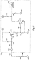
- FIG. 1 a partial view of an exemplary embodiment of an input device in accordance with the disclosure is shown in Fig. 1 and is designated generally by reference character 100.
- the systems and methods described herein can be used to provide discrete input to a logic device indicative of the state of a load independent of the voltage supplied to the load.
- the input device 100 includes an input line 102 with a voltage divider node 110 for connecting a load 106 to the input line 102 for providing input regarding state of the load 106.
- the cathode C of a first diode 130 is connected to the input line 102 to protect the input device 100 from lightning and other transients.
- a first resistor 108 is connected between the voltage divider node 110 and the voltage source V1, e.g., a voltage source for the load 106, or first voltage source, and is used for creating a voltage drop across the emitter E and base B of a PNP style transistor 114, i.e., the first transistor 114, when a load 106 is connected to the input device 100.
- the voltage drop across the base B and emitter E of the PNP style transistor 114 causes the PNP style transistor 114 to close.
- voltage source V1 provides current to a third resistor 124.
- a second resistor 112 is connected between the voltage divider node 110 and the anode A of the first diode 130 and is used for limiting the current provided to the load 106 from voltage source V1.
- the base B of the first transistor 114 is connected to a fourth resistor 128 that limits the current into the base B of the first transistor 114.
- the emitter E of first transistor 114 is connected to the voltage source V1.
- the collector C of first transistor 114 is connected to the anode A of a second diode 132.
- the second diode 132 is used to protect the input device 100 from negative lightning transients or the like.
- a voltage is developed across base B and emitter E of a NPN style transistor 140, i.e., the second transistor 140.
- the voltage across the base B and emitter E of second transistor 140 causes the second transistor 140 to close.
- a fifth resistor 126 is connected between the base B of second transistor 140 and the cathode C of the second diode 132 and is used to limit the current into the base of second transistor 140.
- the emitter E of the second transistor 140 is connected to ground 104.
- the collector C of the second transistor 140 is connected to the input of the logic device 116.
- a sixth resistor 118 is connected between the second voltage source V2, a voltage source for the input, and the collector C of second transistor 140 and is used to limit the current through second transistor 140.
- a capacitor 134 is connected between the input to the logic device 116 and ground 104 and is used to provide a time delay to the logic device 116 to prevent the logic device 116 from responding to noise or other short duration voltage spikes at the input line 102.
- the voltage source V2 provides the input voltage to the logic device 116 depending on the state of the second transistor 140.
- the load 106, the third resistor 124, the capacitor 134, and the emitter E of second transistor 140 are all connected to a single, common ground 104.
- a method of providing a discrete input to a logic device, e.g., logic device 116, regarding state of a load, e.g. whether load 106 is high impedance or low impedance includes powering an input line connected to a load, e.g., input line 102, and to a first switching component 114 to allow current through the first switching component 114, e.g. first transistor 114, which will then control a second switching component 140, e.g. second transistor 140, which controls the input to the logic device provided by a second voltage source.
- the method includes switching the switching component based on voltage on the input line to provide discrete input to the logic device regarding state of the load independent of voltage supplied to the input line.
- Providing discrete input to a logic device can include determining whether or not a voltage is applied across a resistor, e.g. across resistor 124.
- Ground/open discrete input uses two transistors to decouple the logic device that drives the status signal for the discrete input. This provides a tunable ground/open discrete input that meets ground/open indications requirement over the entire range of supply voltages.
- the status signal is supplied by a separate source, e.g. voltage source V2, than the wetting current source for the load, e.g., voltage source V1. This allows requirements for logic high and logic low to be met for the logic device over the whole range of supply voltages from voltage source V1.
- Conventional techniques rely on the wetting current source to be divided down to meet the threshold requirements of the logic device that drives that status signal.
Landscapes
- Engineering & Computer Science (AREA)
- Computer Hardware Design (AREA)
- Physics & Mathematics (AREA)
- Computing Systems (AREA)
- General Engineering & Computer Science (AREA)
- Mathematical Physics (AREA)
- Logic Circuits (AREA)
- Electronic Switches (AREA)
Abstract
Description
- The present disclosure relates to inputs for logic components, and more particularly to ground open inputs and voltage open inputs.
- Conventional topologies for ground open inputs provide a 'ground' indication to a logic component if a monitored load is connected (or provides a path to ground) and to provide an 'open' indication if the monitored load is not connected (or does not provide a path to ground). It is also a requirement to provide a specified current to the load. The conventional topologies are restricted in their operating range when the circuit has a power supply voltage that varies over a wide range. This problem is exacerbated by tolerance of the input voltage thresholds that are required by individual logic devices to register a logic high or logic low. Therefore, a conventional circuit must register a logic low when the voltage supply is at its maximum voltage while the logic input threshold is at its minimum voltage, as well as register a logic high when the voltage supply is at its minimum voltage while the logic input threshold is at its maximum voltage.
- The conventional techniques have been considered satisfactory for their intended purpose. However, there is an ever present need for improved input devices. This disclosure provides a solution for this problem.
- An input device includes an input line connected to a voltage divider node for connecting a load to the voltage divider node. A first switching component is connected to the voltage divider node. A first resistor is connected to the voltage divider node for connecting a first voltage source to the input line. A second resistor is connected between the input line and the voltage divider node for limiting current to the load, wherein the first voltage source is also connected to the first switching component. A second switching component is operatively connected to the first switching component, wherein the second switching component is configured to connect an second voltage source to a logic device for discrete input to the logic device that is decoupled from voltage supplied to the input line by the first voltage source for providing logic high and low input regardless of voltage supplied by the first voltage source.
- The first switching component can include a first transistor having a base, collector, and emitter, wherein the base of the transistor is connected to the voltage divider node, wherein the collector is configured to be connected to ground, and wherein the emitter is configured to be connected to a first voltage source. The second switching component can include a second transistor having a base, collector, and emitter, wherein the base of the second transistor is connected to the collector of the first transistor, wherein the collector of the second transistor is configured to connect to the second voltage source, and wherein the emitter of the second transistor is configured to be connected to ground.
- A logic device can be operatively connected to the collector of the second transistor. A third resistor can be connected to the collector of the second transistor for connecting the second voltage source to the second transistor. The first and third resistors can be configured to be connected to separate voltage sources from one another. The logic device can be connected to the collector of the second transistor to register a logic high when the second transistor is open and to register a logic low when the second transistor is closed.
- A fourth resistor can be connected to the collector of the first transistor for limiting the current through the first transistor. A fourth resistor can be connected to the base of the first transistor to limit the base current for the first transistor. A fifth resistor can be connected to the base of the second transistor to limit base current for the second transistor. A sixth resistor can be connected to the collector of the second transistor for limiting the current through the second transistor. A first diode can be connected to the input line to block unwanted voltage inputs and/or lightning transients. A second diode can be connected to the collector of the first transistor to block negative lightning events. A capacitor can be connected to the collector of the second transistor to ground to add a switching delay to the logic device.
- A first voltage source can be operatively connected to the first resistor and a second voltage source separate from the first voltage source operatively connected to the second switching component. A load can be operatively connected to the input line.
- A method of providing discrete input to a logic device regarding state of a load includes powering an input line connected to a load and to a switching component to allow current through the switching component. The method also includes switching the switching component based on voltage on the input line to provide discrete input to a logic device regarding the state of the load independent of voltage supplied to the input line. The switching component can include a transistor, wherein the base of the transistor is connected to the input line for switching current through a resistor, wherein providing discrete input to a logic device includes determining whether or not a voltage is applied across the resistor.
- These and other features of the systems and methods of the subject disclosure will become more readily apparent to those skilled in the art from the following detailed description of the preferred embodiments taken in conjunction with the drawings.
- So that those skilled in the art to which the subject disclosure appertains will readily understand how to make and use the devices and methods of the subject disclosure without undue experimentation, preferred embodiments thereof will be described in detail herein below with reference to certain figures, wherein:
-
Fig. 1 is a schematic view of an exemplary embodiment of an input device constructed in accordance with the present disclosure, showing two options for operatively connecting a logic device to receive a discrete input independent of the voltage supplied to the input line. - Reference will now be made to the drawings wherein like reference numerals identify similar structural features or aspects of the subject disclosure. For purposes of explanation and illustration, and not limitation, a partial view of an exemplary embodiment of an input device in accordance with the disclosure is shown in
Fig. 1 and is designated generally byreference character 100. The systems and methods described herein can be used to provide discrete input to a logic device indicative of the state of a load independent of the voltage supplied to the load. - The
input device 100 includes aninput line 102 with avoltage divider node 110 for connecting aload 106 to theinput line 102 for providing input regarding state of theload 106. The cathode C of afirst diode 130 is connected to theinput line 102 to protect theinput device 100 from lightning and other transients. Afirst resistor 108 is connected between thevoltage divider node 110 and the voltage source V1, e.g., a voltage source for theload 106, or first voltage source, and is used for creating a voltage drop across the emitter E and base B of aPNP style transistor 114, i.e., thefirst transistor 114, when aload 106 is connected to theinput device 100. The voltage drop across the base B and emitter E of thePNP style transistor 114 causes thePNP style transistor 114 to close. When thisfirst transistor 114 closes, voltage source V1 provides current to athird resistor 124. Asecond resistor 112 is connected between thevoltage divider node 110 and the anode A of thefirst diode 130 and is used for limiting the current provided to theload 106 from voltage source V1. The base B of thefirst transistor 114 is connected to afourth resistor 128 that limits the current into the base B of thefirst transistor 114. The emitter E offirst transistor 114 is connected to the voltage source V1. The collector C offirst transistor 114 is connected to the anode A of asecond diode 132. Thesecond diode 132 is used to protect theinput device 100 from negative lightning transients or the like. When thefirst transistor 114 closes and allows voltage source V1 to provide current to thethird resistor 124, a voltage is developed across base B and emitter E of aNPN style transistor 140, i.e., thesecond transistor 140. The voltage across the base B and emitter E ofsecond transistor 140 causes thesecond transistor 140 to close. Afifth resistor 126 is connected between the base B ofsecond transistor 140 and the cathode C of thesecond diode 132 and is used to limit the current into the base ofsecond transistor 140. The emitter E of thesecond transistor 140 is connected toground 104. The collector C of thesecond transistor 140 is connected to the input of thelogic device 116. Asixth resistor 118 is connected between the second voltage source V2, a voltage source for the input, and the collector C ofsecond transistor 140 and is used to limit the current throughsecond transistor 140. Acapacitor 134 is connected between the input to thelogic device 116 andground 104 and is used to provide a time delay to thelogic device 116 to prevent thelogic device 116 from responding to noise or other short duration voltage spikes at theinput line 102. The voltage source V2 provides the input voltage to thelogic device 116 depending on the state of thesecond transistor 140. Theload 106, thethird resistor 124, thecapacitor 134, and the emitter E ofsecond transistor 140 are all connected to a single,common ground 104. - When a
low impedance load 106 is connected to theinput line 102 of theinput device 100, a voltage is developed acrossresistor 108 which causes thefirst transistor 114 to close. Whenfirst transistor 114 closes, current flows throughresistor 124 and causes thesecond transistor 140 to close. Whensecond transistor 140 closes, the input voltage of thelogic device 116, supplied by voltage source V2, is pulled to ground 104, providing a logic low as input toinput device 116. - When a
high impedance load 106 is connected to theinput line 102 of theinput device 100, there is no voltage drop across theresistor 108. This causesfirst transistor 114 to be in the open state. Whenfirst transistor 114 is in the open state, no current flows through thethird resistor 124 and therefore, there is no voltage drop across thethird resistor 124. With no voltage drop acrossresistor 124, thesecond transistor 140 is in open state. When thesecond transistor 140 is in the open state, there is no current draw through thesixth resistor 118 and the input voltage to the logic device is at the same level as the voltage source V2, providing a logic high as input toinput device 116. - A method of providing a discrete input to a logic device, e.g.,
logic device 116, regarding state of a load, e.g. whetherload 106 is high impedance or low impedance, includes powering an input line connected to a load, e.g.,input line 102, and to afirst switching component 114 to allow current through thefirst switching component 114, e.g.first transistor 114, which will then control asecond switching component 140, e.g.second transistor 140, which controls the input to the logic device provided by a second voltage source. The method includes switching the switching component based on voltage on the input line to provide discrete input to the logic device regarding state of the load independent of voltage supplied to the input line. Providing discrete input to a logic device can include determining whether or not a voltage is applied across a resistor, e.g. acrossresistor 124. - Ground/open discrete input as disclosed herein uses two transistors to decouple the logic device that drives the status signal for the discrete input. This provides a tunable ground/open discrete input that meets ground/open indications requirement over the entire range of supply voltages. The status signal is supplied by a separate source, e.g. voltage source V2, than the wetting current source for the load, e.g., voltage source V1. This allows requirements for logic high and logic low to be met for the logic device over the whole range of supply voltages from voltage source V1. Conventional techniques rely on the wetting current source to be divided down to meet the threshold requirements of the logic device that drives that status signal.
- The methods and systems of the present disclosure, as described above and shown in the drawings, provide for discrete input with superior properties including decoupling the voltage supplied to the load and input line from the voltage source for the input to the logic device. While the apparatus and methods of the subject disclosure have been shown and described with reference to preferred embodiments, those skilled in the art will readily appreciate that changes and/or modifications may be made thereto without departing from the scope of the subject disclosure.
Claims (15)
- An input device (100) comprising:an input line (102) connected to a voltage divider node (110) for connecting a load (106) to the voltage divider node (110) ;a first switching component (114) connected to the voltage divider node (110);a first resistor (108) connected to the voltage divider node (110) for connecting a first voltage source to the input line (102);a second resistor (112) connected between the input line (102) and the voltage divider node (110) for limiting current to the load (106), wherein the first voltage source is also connected to the first switching component; anda second switching component (140) operatively connected to the first switching component (114), wherein the second switching component (140) is configured to connect a second voltage source to a logic device (116) for discrete input to the logic device (116) that is decoupled from voltage supplied to the input line (102) by the first voltage source for providing logic high and low input regardless of voltage supplied by the first voltage source.
- The input device as recited in claim 1, wherein the first switching component (114) includes a first transistor (114) having a base, collector, and emitter, wherein the base of the first transistor (114) is connected to the voltage divider node (110), wherein the collector is configured to be connected to ground, and wherein the emitter is configured to be connected to the first voltage source, and wherein the second switching component (140) includes a second transistor having a base, collector, and emitter, wherein the base of the second transistor (140) is connected to the collector of the first transistor (114), wherein the collector of the second transistor (140) is configured to connect to the second voltage source, and wherein the emitter of the second transistor (140) is configured to be connected to ground.
- The input device as recited in claim 2, further comprising:
a logic device (116) operatively connected to the collector of the second transistor (140). - The input device as recited in claim 3, further comprising:
a third resistor (124) connected to the collector of the second transistor (140) for connecting the second voltage source to the second transistor (140). - The input device as recited in claim 4, wherein the first (108) and third resistors (124) are configured to be connected to separate voltage sources from one another.
- The input device as recited in claim 4, wherein the logic device (116) is connected to the collector of the second transistor (140) to register a logic high when the second transistor (140) is open and to register a logic low when the second transistor (140) is closed.
- The input device as recited in claim 3, further comprising:
a fourth resistor (128) connected to the collector of the first transistor (108) for limiting the current through the first transistor (108). - The input device as recited in claim 7, further comprising:
a fourth resistor (128) connected to the base of the first transistor (108) to limit the base current for the first transistor (108). - The input device as recited in claim 8, further comprising:
a fifth resistor (126) connected to the base of the second transistor (140) to limit base current for the second transistor (140), and preferably further comprising:
a sixth resistor (118) connected to the collector of the second transistor (140) for limiting the current through the second transistor (140). - The input device as recited in claim 2, further comprising:
a first diode (130) connected to the input line (102) to block unwanted voltage inputs and/or lightning transients, and preferably further comprising:
a second diode (132) connected to the collector of the first transistor (108) to block negative lightning events. - The input device as recited in claim 2, further comprising:
a capacitor (134) connecting the collector of the second transistor (140) to ground to add a switching delay to the logic device (116). - The input device as recited in any proceeding claim, further comprising:
a first voltage source operatively connected to the first resistor (108) and a second voltage source separate from the first voltage source operatively connected to the second switching component (140). - The input device as recited in any proceeding claim, further comprising:
a load (106) operatively connected to the input line (102) of the input device (100). - A method of providing discrete input to a logic device regarding state of a load comprising:powering an input line (102) connected to a load and to a switching component (114) to allow current through the switching component (114); andswitching the switching component (114) based on voltage on the input line (102) to provide discrete input to a logic device (116) regarding state of the load independent of voltage supplied to the input line (102).
- A method as recited in claim 14, wherein the switching component (114) includes a transistor (114), wherein a base of the transistor (114) is connected to the input line (102) for switching current through a resistor (108), wherein providing discrete input to a logic device (118) includes determining whether or not a voltage is applied across the resistor (108).
Applications Claiming Priority (1)
| Application Number | Priority Date | Filing Date | Title |
|---|---|---|---|
| US15/586,748 US10374601B2 (en) | 2017-05-04 | 2017-05-04 | Discrete input |
Publications (1)
| Publication Number | Publication Date |
|---|---|
| EP3399322A1 true EP3399322A1 (en) | 2018-11-07 |
Family
ID=62217736
Family Applications (1)
| Application Number | Title | Priority Date | Filing Date |
|---|---|---|---|
| EP18170706.8A Ceased EP3399322A1 (en) | 2017-05-04 | 2018-05-03 | Discrete input |
Country Status (2)
| Country | Link |
|---|---|
| US (1) | US10374601B2 (en) |
| EP (1) | EP3399322A1 (en) |
Citations (2)
| Publication number | Priority date | Publication date | Assignee | Title |
|---|---|---|---|---|
| DE19920465C1 (en) * | 1999-05-04 | 2000-11-02 | Siemens Ag | Procedure for open-load diagnosis of a switching stage |
| US9474113B2 (en) * | 2014-05-16 | 2016-10-18 | Enerton, Inc. | Dimmable universal voltage LED power supply with regenerating power source circuitry and non-isolated load |
Family Cites Families (5)
| Publication number | Priority date | Publication date | Assignee | Title |
|---|---|---|---|---|
| US7061734B2 (en) | 2003-02-14 | 2006-06-13 | Visteon Global Technologies, Inc. | Class II bus negative transient protection |
| US7233165B2 (en) | 2005-03-31 | 2007-06-19 | Seiko Epson Corporation | High speed driver for serial communications |
| DE102007027505B3 (en) | 2007-06-11 | 2009-01-08 | Minebea Co., Ltd. | Control circuit for a high-side semiconductor switch for switching a supply voltage |
| CN204013450U (en) | 2014-08-29 | 2014-12-10 | 杭州士兰微电子股份有限公司 | Be applicable to the drain circuit of opening on the floating ground of high pressure |
| US9537338B2 (en) | 2014-09-16 | 2017-01-03 | Navitas Semiconductor Inc. | Level shift and inverter circuits for GaN devices |
-
2017
- 2017-05-04 US US15/586,748 patent/US10374601B2/en active Active
-
2018
- 2018-05-03 EP EP18170706.8A patent/EP3399322A1/en not_active Ceased
Patent Citations (2)
| Publication number | Priority date | Publication date | Assignee | Title |
|---|---|---|---|---|
| DE19920465C1 (en) * | 1999-05-04 | 2000-11-02 | Siemens Ag | Procedure for open-load diagnosis of a switching stage |
| US9474113B2 (en) * | 2014-05-16 | 2016-10-18 | Enerton, Inc. | Dimmable universal voltage LED power supply with regenerating power source circuitry and non-isolated load |
Also Published As
| Publication number | Publication date |
|---|---|
| US10374601B2 (en) | 2019-08-06 |
| US20180323782A1 (en) | 2018-11-08 |
Similar Documents
| Publication | Publication Date | Title |
|---|---|---|
| US9152197B2 (en) | Overcurrent protection circuit and server using the same | |
| US11114838B2 (en) | Ideal diode with active reverse voltage protection | |
| EP2933646B1 (en) | Precision measurement of voltage drop across a semiconductor switching element | |
| EP2071690A2 (en) | Overvoltage protection circuit and electronic device comprising the same | |
| CN110658481B (en) | Grounding loss detection system | |
| KR101751315B1 (en) | Self-sustaining, high voltage tolerant power supply | |
| US20200144808A1 (en) | Direct-current voltage supply circuit | |
| JP2016001822A (en) | Load drive circuit | |
| CN118176667B (en) | Power switch with normally-on transistor | |
| JPWO2019008817A1 (en) | Short circuit protection circuit for semiconductor switching devices | |
| CN110855130B (en) | Power supply input clamping circuit and chip | |
| US20140084878A1 (en) | Power supply switching circuit | |
| CN108512191B (en) | Surge protection circuit, electronic equipment and surge protection method of circuit | |
| EP3399616B1 (en) | Ground/voltage open input | |
| US7932628B2 (en) | Control device with terminal 15—holding circuit | |
| US10374601B2 (en) | Discrete input | |
| US10396661B2 (en) | Power supply control apparatus | |
| US10498330B1 (en) | Low leakage switch control circuit | |
| WO2020108297A1 (en) | Detection and protection circuit of active device, and power supply circuit and method | |
| CN209896689U (en) | Over-temperature protection circuit and switching power supply circuit | |
| CN113702796A (en) | Semiconductor device desaturation state detection circuit | |
| CN222735868U (en) | Current backflow prevention circuit, dual power supply current backflow prevention circuit and electronic equipment | |
| CN222721184U (en) | Dual-power supply circuit and electronic equipment | |
| CN109710011A (en) | A kind of low-power consumption dummy load circuit | |
| KR101668653B1 (en) | Control unit for protecting an internal device from battery short-circuit |
Legal Events
| Date | Code | Title | Description |
|---|---|---|---|
| PUAI | Public reference made under article 153(3) epc to a published international application that has entered the european phase |
Free format text: ORIGINAL CODE: 0009012 |
|
| STAA | Information on the status of an ep patent application or granted ep patent |
Free format text: STATUS: THE APPLICATION HAS BEEN PUBLISHED |
|
| AK | Designated contracting states |
Kind code of ref document: A1 Designated state(s): AL AT BE BG CH CY CZ DE DK EE ES FI FR GB GR HR HU IE IS IT LI LT LU LV MC MK MT NL NO PL PT RO RS SE SI SK SM TR |
|
| AX | Request for extension of the european patent |
Extension state: BA ME |
|
| RIN1 | Information on inventor provided before grant (corrected) |
Inventor name: BLAZER, CHRISTOPHER |
|
| STAA | Information on the status of an ep patent application or granted ep patent |
Free format text: STATUS: REQUEST FOR EXAMINATION WAS MADE |
|
| 17P | Request for examination filed |
Effective date: 20190507 |
|
| RBV | Designated contracting states (corrected) |
Designated state(s): AL AT BE BG CH CY CZ DE DK EE ES FI FR GB GR HR HU IE IS IT LI LT LU LV MC MK MT NL NO PL PT RO RS SE SI SK SM TR |
|
| STAA | Information on the status of an ep patent application or granted ep patent |
Free format text: STATUS: EXAMINATION IS IN PROGRESS |
|
| 17Q | First examination report despatched |
Effective date: 20210429 |
|
| STAA | Information on the status of an ep patent application or granted ep patent |
Free format text: STATUS: THE APPLICATION HAS BEEN REFUSED |
|
| 18R | Application refused |
Effective date: 20230101 |