EP3399288B1 - Camera assembly and mobile electronic device - Google Patents
Camera assembly and mobile electronic device Download PDFInfo
- Publication number
- EP3399288B1 EP3399288B1 EP18170252.3A EP18170252A EP3399288B1 EP 3399288 B1 EP3399288 B1 EP 3399288B1 EP 18170252 A EP18170252 A EP 18170252A EP 3399288 B1 EP3399288 B1 EP 3399288B1
- Authority
- EP
- European Patent Office
- Prior art keywords
- illumination intensity
- light sensing
- camera assembly
- region
- imaging
- Prior art date
- Legal status (The legal status is an assumption and is not a legal conclusion. Google has not performed a legal analysis and makes no representation as to the accuracy of the status listed.)
- Active
Links
- 238000005286 illumination Methods 0.000 claims description 255
- 238000003384 imaging method Methods 0.000 claims description 145
- 230000000712 assembly Effects 0.000 claims description 34
- 238000000429 assembly Methods 0.000 claims description 34
- 238000010586 diagram Methods 0.000 description 11
- 238000001514 detection method Methods 0.000 description 9
- 230000008859 change Effects 0.000 description 5
- 238000000034 method Methods 0.000 description 3
- 238000012545 processing Methods 0.000 description 3
- 238000004458 analytical method Methods 0.000 description 2
- 239000011159 matrix material Substances 0.000 description 2
- 238000005259 measurement Methods 0.000 description 2
- 230000008569 process Effects 0.000 description 2
- 230000004044 response Effects 0.000 description 2
- 230000035945 sensitivity Effects 0.000 description 2
- 238000003491 array Methods 0.000 description 1
- 230000007423 decrease Effects 0.000 description 1
- 230000001419 dependent effect Effects 0.000 description 1
- 230000000694 effects Effects 0.000 description 1
- 230000005611 electricity Effects 0.000 description 1
- 230000010365 information processing Effects 0.000 description 1
- 238000012805 post-processing Methods 0.000 description 1
- 238000003825 pressing Methods 0.000 description 1
- 238000003672 processing method Methods 0.000 description 1
- 239000004065 semiconductor Substances 0.000 description 1
- 239000000758 substrate Substances 0.000 description 1
Images


Classifications
-
- H—ELECTRICITY
- H04—ELECTRIC COMMUNICATION TECHNIQUE
- H04M—TELEPHONIC COMMUNICATION
- H04M1/00—Substation equipment, e.g. for use by subscribers
- H04M1/02—Constructional features of telephone sets
- H04M1/0202—Portable telephone sets, e.g. cordless phones, mobile phones or bar type handsets
- H04M1/026—Details of the structure or mounting of specific components
- H04M1/0264—Details of the structure or mounting of specific components for a camera module assembly
-
- H—ELECTRICITY
- H04—ELECTRIC COMMUNICATION TECHNIQUE
- H04N—PICTORIAL COMMUNICATION, e.g. TELEVISION
- H04N23/00—Cameras or camera modules comprising electronic image sensors; Control thereof
- H04N23/60—Control of cameras or camera modules
- H04N23/66—Remote control of cameras or camera parts, e.g. by remote control devices
-
- H—ELECTRICITY
- H04—ELECTRIC COMMUNICATION TECHNIQUE
- H04N—PICTORIAL COMMUNICATION, e.g. TELEVISION
- H04N23/00—Cameras or camera modules comprising electronic image sensors; Control thereof
- H04N23/45—Cameras or camera modules comprising electronic image sensors; Control thereof for generating image signals from two or more image sensors being of different type or operating in different modes, e.g. with a CMOS sensor for moving images in combination with a charge-coupled device [CCD] for still images
-
- G—PHYSICS
- G01—MEASURING; TESTING
- G01J—MEASUREMENT OF INTENSITY, VELOCITY, SPECTRAL CONTENT, POLARISATION, PHASE OR PULSE CHARACTERISTICS OF INFRARED, VISIBLE OR ULTRAVIOLET LIGHT; COLORIMETRY; RADIATION PYROMETRY
- G01J1/00—Photometry, e.g. photographic exposure meter
- G01J1/42—Photometry, e.g. photographic exposure meter using electric radiation detectors
- G01J1/4204—Photometry, e.g. photographic exposure meter using electric radiation detectors with determination of ambient light
-
- G—PHYSICS
- G01—MEASURING; TESTING
- G01J—MEASUREMENT OF INTENSITY, VELOCITY, SPECTRAL CONTENT, POLARISATION, PHASE OR PULSE CHARACTERISTICS OF INFRARED, VISIBLE OR ULTRAVIOLET LIGHT; COLORIMETRY; RADIATION PYROMETRY
- G01J3/00—Spectrometry; Spectrophotometry; Monochromators; Measuring colours
- G01J3/46—Measurement of colour; Colour measuring devices, e.g. colorimeters
- G01J3/50—Measurement of colour; Colour measuring devices, e.g. colorimeters using electric radiation detectors
- G01J3/505—Measurement of colour; Colour measuring devices, e.g. colorimeters using electric radiation detectors measuring the colour produced by lighting fixtures other than screens, monitors, displays or CRTs
-
- H—ELECTRICITY
- H04—ELECTRIC COMMUNICATION TECHNIQUE
- H04N—PICTORIAL COMMUNICATION, e.g. TELEVISION
- H04N23/00—Cameras or camera modules comprising electronic image sensors; Control thereof
- H04N23/50—Constructional details
- H04N23/54—Mounting of pick-up tubes, electronic image sensors, deviation or focusing coils
-
- H—ELECTRICITY
- H04—ELECTRIC COMMUNICATION TECHNIQUE
- H04N—PICTORIAL COMMUNICATION, e.g. TELEVISION
- H04N23/00—Cameras or camera modules comprising electronic image sensors; Control thereof
- H04N23/50—Constructional details
- H04N23/55—Optical parts specially adapted for electronic image sensors; Mounting thereof
-
- H—ELECTRICITY
- H04—ELECTRIC COMMUNICATION TECHNIQUE
- H04N—PICTORIAL COMMUNICATION, e.g. TELEVISION
- H04N23/00—Cameras or camera modules comprising electronic image sensors; Control thereof
- H04N23/57—Mechanical or electrical details of cameras or camera modules specially adapted for being embedded in other devices
-
- H—ELECTRICITY
- H04—ELECTRIC COMMUNICATION TECHNIQUE
- H04N—PICTORIAL COMMUNICATION, e.g. TELEVISION
- H04N23/00—Cameras or camera modules comprising electronic image sensors; Control thereof
- H04N23/60—Control of cameras or camera modules
- H04N23/68—Control of cameras or camera modules for stable pick-up of the scene, e.g. compensating for camera body vibrations
- H04N23/681—Motion detection
-
- H—ELECTRICITY
- H04—ELECTRIC COMMUNICATION TECHNIQUE
- H04N—PICTORIAL COMMUNICATION, e.g. TELEVISION
- H04N23/00—Cameras or camera modules comprising electronic image sensors; Control thereof
- H04N23/70—Circuitry for compensating brightness variation in the scene
- H04N23/71—Circuitry for evaluating the brightness variation
-
- H—ELECTRICITY
- H04—ELECTRIC COMMUNICATION TECHNIQUE
- H04N—PICTORIAL COMMUNICATION, e.g. TELEVISION
- H04N25/00—Circuitry of solid-state image sensors [SSIS]; Control thereof
- H04N25/70—SSIS architectures; Circuits associated therewith
- H04N25/702—SSIS architectures characterised by non-identical, non-equidistant or non-planar pixel layout
-
- H—ELECTRICITY
- H04—ELECTRIC COMMUNICATION TECHNIQUE
- H04N—PICTORIAL COMMUNICATION, e.g. TELEVISION
- H04N25/00—Circuitry of solid-state image sensors [SSIS]; Control thereof
- H04N25/70—SSIS architectures; Circuits associated therewith
- H04N25/703—SSIS architectures incorporating pixels for producing signals other than image signals
Definitions
- the present disclosure relates to electronic devices, and more particularly to a camera assembly, and a mobile electronic device.
- a front camera can be set on a phone to capture a selfie
- a light sensor can be set to adjust display brightness of a screen of the phone according to ambient brightness.
- a large space would be occupied by them, such that the space for locating the display screen in the phone decreases, thus leading to a low screen-to-body ratio.
- US2012092541A1 discloses a method and apparatus for ambient light measurement system.
- the apparatus includes a display and a combined camera and ambient light measurement arrangement having photosensitive elements.
- the arrangement is configured to operate in a first power mode and a second different power mode.
- US2012176533A1 discloses an imaging device including a fixed focused lens, an image sensor having an image matrix of a plurality of pixels arranged on a semiconductor substrate and supplying image data, and electronic means for reading the image matrix.
- US2016037070A1 discloses a multi-mode power-effective light and gesture sensing in image sensors, the image sensor includes a read-out integrated circuit, a plurality of pixel electrodes, an optically sensitive layer, and a top electrical contact.
- electrical current passing through the top electrical contact is configured to be sensed, and independent currents passing through the plurality of pixel electrodes are configured not to be sensed independently.
- US9497367B1 discloses a maximizing effective surface area of a rectangular image sensor concurrently capturing image data from two lenses. Each of the two lenses can produce a corresponding image circle simultaneously on the rectangular image sensor. An area of the image circles from the two lenses can be non-overlapping.
- the image sensor can be a device which converts light within the real world environment into electronic signals.
- US2015046505A1 discloses an information processing method and electronic device, comprising: acquiring a first value of a first parameter by the first sensor; acquiring a second value of the first parameter by the second sensor; judging whether a difference value between the first value and the second value is larger than or equal to a first threshold or not.
- US2013076712A1 discloses distributed light sensors for ambient light detection, in which, when a touch sensor signal indicates that an external object is covering one of the ambient light sensors, data from that ambient light sensor can be discarded.
- the ambient light sensors may include a primary ambient light sensor such as a human-eye-response ambient light sensor and may include an array of secondary ambient light sensors such as non-human-eye-response sensors.
- US2015092066 discloses using a second camera to adjust settings of a first camera.
- Embodiments of the present disclosure provide a camera assembly and a mobile electronic device.
- the camera assembly according to the invention is set out in independent claim 1.
- the mobile electronic device according the invention is defined in claim 3.
- a structure in which a first feature is "on" a second feature may include an embodiment in which the first feature directly contacts the second feature, and may also include an embodiment in which the first feature indirectly contacts the second feature via an intermediate medium.
- a structure in which a first feature is "on”, “over” or “above” a second feature may indicate that the first feature is right above the second feature or obliquely above the second feature, or just indicate that a horizontal level of the first feature is higher than the second feature.
- a structure in which a first feature is "below”, or “under” a second feature may indicate that the first feature is right under the second feature or obliquely under the second feature, or just indicate that a horizontal level of the first feature is lower than the second feature.
- the camera assembly 100 includes two lens assemblies 10.
- Each lens assembly 10 includes an image sensor 12.
- Each image sensor 12 includes a pixel array 122 and a control circuit 124.
- the pixel array 122 includes a light sensing region 1222 and an imaging region 1224.
- the control circuit 124 is configured to control the light sensing region 1222 to detect an illumination intensity when a light sensing instruction is received.
- the control circuit 124 is further configured to control the imaging region 1224 to obtain an image when an imaging instruction is received.
- the lens assembly 10 further includes a filter 14.
- the filter 14 and the imaging region 1224 are arranged correspondingly. Light would reach the imaging region 1224 after passing through the filter 14.
- the filter 14 may be an RGB filter 14.
- the RGB filter 14 can be arranged in Bayer array to allow light L to pass through the filter 14 and pass through the imaging region 1224, so as to obtain a color image.
- the lens assembly 10 may further include a visible filter.
- the visible filter and the light sensing region 1222 are arranged correspondingly to allow light L to pass through the visible filter and to reach the light sensing region 1222.
- visible light of the light L can reach the light sensing region 1222, such that the light sensing region 1222 can detect the illumination intensity of the visible light, thus avoiding interference of invisible light such as infrared light, ultraviolet light or the like in the light L.
- the camera assembly 100 can be applied in an electronic device 1000 according to embodiments of the present disclosure.
- the electronic device 1000 further includes a processor 200.
- the processor 200 is configured to generate the light sensing instruction and the imaging instruction.
- the electronic device 1000 further includes a display screen 300.
- the display screen 300 is configured to display data information such as video, image, text, icon and the like.
- control circuit 124 can realize both detection of the illumination intensity and acquisition of the image by controlling the pixel array 122. In this way, it is unnecessary to set both a camera component and a light sensor component, such that the number of components is reduced, a ratio of space for locating the display screen 300 can be increased, thus increasing the screen-to-body ratio of the electronic device 1000.
- two lens assemblies 10 include a main lens assembly and a secondary lens assembly.
- An area of the imaging region of the main lens assembly is larger than an area of the imaging region of the secondary lens assembly, such that the main lens assembly can realize a better imaging quality.
- an area of the pixel array 122 of the main lens assembly can be the same as or be different from an area of the pixel array 122 of secondary lens assembly.
- the electronic device 1000 may be a cell phone, a tablet computer, a smart watch or the like.
- the electronic device 1000 according to embodiments of the present will be explained by taking a cell phone as an example.
- the illumination intensity detected by the camera assembly 100 can be considered as the basis for adjusting display brightness of the display screen 300 of the electronic device 1000. For example, when the illumination intensity is high, the display brightness of the display screen 300 can be increased. When the illumination intensity is changed from a high value to a value less than a certain threshold, it can be determined that a user is answering the phone, such that the display screen 300 can be turned off.
- the image obtained by the camera assembly 10 can be displayed on the display screen 300, or stored in storage medium of the electronic device 1000 for reading or transmitting.
- the camera assembly 100 together with the display screen 300 can be set on a front face 400 of the electronic device 1000.
- the camera assembly 100 can also be disposed on a back face 500 or side face of the electronic device 1000.
- the two lens assemblies 10 of the camera assembly 100 can be arranged laterally or longitudinally.
- the processor 200 is configured to generate the light sensing instruction and the imaging instruction. Further, the processor 200 is configured to transmit the light sensing instruction and the imaging instruction to the control circuit 124. In some embodiments, the processor 200 can separately generate and transmit the light sensing instruction, or separately generate and transmit the imaging instruction, or simultaneously generate and transmit the light sensing instruction and the imaging instruction.
- the light sensing instruction and the imaging instruction can be generated by the processor 200 when receiving an input operation.
- the input operation can be an operation inputted by the user or by an application environment.
- the light sensing instruction and the imaging instruction can be generated by the processor 200 after receiving an operation of touching the cell phone or pressing a certain function key (including a physical key, a virtual key) from the user.
- the light sensing instruction and the imaging instruction can be generated by the processor 200 when the system time of the cell phone reaches a predetermined time point.
- a single control circuit 124 can receive the light sensing instruction and the imaging instruction simultaneously. In other words, the control circuit 124 can simultaneously control the light sensing region 1222 to detect the illumination intensity and control the imaging region 1224 to acquire the image. Certainly, the control circuit 124 can also be configured to separately receive the light sensing instruction to control the light sensing region 1222 to detect the illumination intensity, or separately receive the imaging instruction to control the imaging region 1224 to acquire the image. When the control circuit 124 does not receive the light sensing instruction and the imaging instruction, the light sensing region 1222 and the imaging region 1224 may be in the non-operating state.
- the two control circuits 124 may receive the light sensing instruction and the imaging instruction separately.
- the camera assembly 100 may generate two light sensing instructions and two imaging instructions, which may be a first light sensing instruction, a second light sensing instruction, a first imaging instruction and a second imaging instruction.
- the first light sensing instruction may be sent only to a first control circuit 124, but not to a second control circuit 124.
- the second light sensing instruction may be sent only to the second control circuit 124, but not to the first control circuit 124.
- the first imaging instruction may be sent only to the first control circuit 124, but not to the second control circuit 124.
- the second imaging instruction may be sent only to the second control circuit 124, but not to the first control circuit 124.
- the two control circuits 124 may receive the light sensing instruction and the imaging instruction simultaneously.
- the camera assembly 100 may generate a light sensing instruction and an imaging instruction.
- the light sensing instruction is sent to the first control circuit 124 and the second control circuit 124 simultaneously.
- one light sensing instruction may be used to control two light sensing regions 1222 to detect the illumination intensity.
- the imaging instruction is sent to the first control circuit 124 and the second control circuit simultaneously.
- one imaging instruction may be used to control two imaging regions 1224 to acquire images.
- the pixel array 122 includes a plurality of pixels arranged in an array.
- the pixels in the light sensing region 1222 are configured to detect the illumination intensity.
- the pixels in the imaging region 1224 are configured to acquire the image.
- Each pixel can generate corresponding electric quantity according to the illumination intensity of light reaching the pixel.
- the control circuit 124 is electrically connected to each pixel.
- the control circuit 124 acquires the electric quantity generated by the corresponding pixel according to the received light sensing instruction or imaging instruction, and further analyzes magnitude of the electric quantity via the processor 200 to obtain the illumination intensity of the light reaching the corresponding pixel or further performs comprehensive analysis on the illumination intensities of light reaching several pixels via the processor 200 to obtain the image.
- the single camera assembly 100 is configured as a front camera assembly 100a.
- the processor 200 is configured to select a maximum of the first illumination intensity and the second illumination intensity as a final illumination intensity; or the processor 200 is configured to obtain a mean value of the first illumination intensity and the second illumination intensity as the final illumination intensity.
- the front camera assembly 100a and the display screen 300 are disposed on the front face 400 of the electronic device 1000.
- the front camera assembly 100a may be configured to detect the illumination intensity on the front face 400 and acquire the image opposite to the front face 400 simultaneously.
- the processor 200 can obtain the final illumination intensity after perform the comprehensive analysis on the first illumination intensity and the second illumination intensity respectively obtained by two light sensing regions 1222.
- the electronic device 1000 further performs corresponding control according to the final illumination intensity, for example adjusting the display brightness of the display screen 300.
- two lens assemblies 10 receive very different illumination intensities.
- one lens assembly 10 may be in the shade while the other lens assembly 10 may be exposed under direct sunlight, such that there may be large difference between the first illumination intensity and the second illumination intensity detected by two light sensing regions 1222.
- the processor 200 processes the first illumination intensity and the second illumination intensity to obtain the final illumination intensity and adjusts the display brightness of the display screen 300 according to the final illumination intensity, thus preventing the display brightness from being too high or too low.
- the two lens assemblies 10 in the front camera assembly 100a may realize imaging simultaneously or on time-sharing.
- the operating state of the front camera assembly 100a may be represented by a combination indicating whether each of the two light sensing regions 1222 and the two imaging regions 1224 is working or not. As illustrated in table 1, if an indication " ⁇ " is used for a light sensing region 1222 or an imaging region 1224, it means that the light sensing region 1222 or the imaging region 1224 is working. If an indication " ⁇ " is used for a light sensing region 1222 or an imaging region 1224, it means that the light sensing region 1222 or the imaging region 1224 is not working. Table 1 No.
- Front camera assembly Image sensor 1 Image sensor 2
- Image sensor 2 Light sensing region Imaging region
- Light sensing region Imaging region 1 ⁇ ⁇ ⁇ ⁇ 2 ⁇ ⁇ ⁇ ⁇ 3 ⁇ ⁇ ⁇ ⁇ 4 ⁇ ⁇ ⁇ ⁇ 5 ⁇ ⁇ ⁇ ⁇ 6 ⁇ ⁇ ⁇ ⁇ 7 ⁇ ⁇ ⁇ ⁇ 8 ⁇ ⁇ ⁇ ⁇ 9 ⁇ ⁇ ⁇ ⁇ ⁇
- the two lens assemblies 10 in the front camera assembly 100a can realize imaging simultaneously to optimize the imaging quality.
- the two lens assemblies 10 in the front camera assembly 100a can realize imaging simultaneously to obtain multiple frames of first images and multiple frames of second images.
- the processor 200 may analyze the multiple frames of first images and the multiple frames of second images and screens out a frame of image with highest imaging quality as a final image.
- the processor 200 may perform merging and splicing processing on the first image and the second image to enhance color and definition of the final image.
- one lens assembly 10 in the front camera assembly 100a may be configured to assist the other lens assembly 10 in imaging, so as to optimize the imaging quality.
- the one lens assembly 10 in the front camera assembly 100a may detect the current ambient brightness, and the processor 200 analyzes the ambient brightness to control exposure time of each light sensor component corresponding to each pixel in the other lens assembly 10 to obtain the image with suitable brightness.
- one lens assembly 10 is used to detect the ambient brightness to assist the other lens assembly 10 in imaging, such that problems that the final image is subject to overexposure or has too low brightness can be avoided, thus improving the image quality.
- the two lens assemblies 10 in the front camera assembly 100a may be enabled in sequence to realize imaging so as to optimize the imaging quality.
- one lens assembly 10 in the front camera assembly 100a adopts a wide-angle lens
- the other lens assembly 10 adopts a telephoto lens.
- the processor 200 enables the lens assembly 10 using the wide-angle lens to realize imaging. If the electronic device 1000 detects that the user takes a scaling-up operation for a preview image and the processor 200 derives an enlarging scale of the preview image higher than a predetermined value, the processor 200 immediately enables the lens assembly 10 using the telephoto lens to realize imaging.
- the wide-angle lens has a big field of view and a short focal length, while the telephoto lens has a small field of view and a long focal length.
- the user takes the scaling-up operation for the preview image, it indicates that the user would like to take a picture of distant view, in this case, it needs to adopt the telephoto lens to get a clear picture of the distant view, thus it needs to switch the camera assembly 100 to the lens assembly 10 using the telephoto lens to realize imaging so as to improve the definition of the image.
- the illumination intensities on the front face 400 and the back face 500 of the electronic device 1000 are different obviously.
- the user may put the electronic device 1000 (e.g. a cell phone) on the table with the front face 400 opposite to the table top.
- the display brightness of the display screen 300 is controlled only according to the illumination intensity on the front face 400 detected by the front camera assembly 100a, the display screen 300 may be in a non-display state or in a low-brightness-display state.
- the electronic device 1000 needs to awaken the display screen 300 or to increase the brightness of the display screen 300 in a short time.
- the electronic device 1000 When the user frequently picks up and puts down the electronic device 1000, the electronic device 1000 would consume a great quantity of electricity energy for controlling the brightness of the display screen 300.
- the back face 500 may be opposite to a light source (such as a ceiling lamp) amounted on the ceiling, such that the illumination intensity on the back face 500 may be greater than that on the front face 400.
- the processor 200 can process both the illumination intensity on the front face 400 and the illumination intensity on the back face 500 of the electronic device 1000, an optimum illumination intensity can be obtained.
- a plurality of camera assemblies 100 there are a plurality of camera assemblies 100.
- One of them is configured as a front camera assembly 100a
- a further of them is configured as a rear camera assembly 100b.
- the front camera assembly 100a and the display screen 300 are disposed on the front face 400 of the electronic device 1000.
- the front camera assembly 100a may be configured to detect the illumination intensity on the front face 400 and acquire the image opposite to the front face 400 simultaneously.
- the rear camera assembly 100b is disposed on the back face 500 of the electronic device 1000.
- the rear camera assembly 100b may be configured to detect the illumination intensity on the back face 500 and acquire the image opposite to the back face 500 simultaneously.
- the operating state of the front camera assembly 100a may be represented by a combination indicating whether each of the light sensing regions 1222 and imaging regions 1224 in the front camera assembly 100a is working or not.
- the operating state of the rear camera assembly 100b may be represented by a combination indicating whether each of the light sensing regions 1222 and imaging regions 1224 in the rear camera assembly 100b is working or not. As illustrated in table 2, if an indication " ⁇ " is used for a light sensing region 1222 or an imaging region 1224, it means that the light sensing region 1222 or the imaging region 1224 is working.
- an indication " ⁇ " is used for a light sensing region 1222 or an imaging region 1224, it means that the light sensing region 1222 or the imaging region 1224 is not working.
- the operating state of the front camera assembly 100a and the operating state of the rear camera assembly 100b are not limited in the following table, there may be other operating states, which are not listed herein. Table 2 No.
- two light sensing regions 1222 in the front camera assembly 100a detect a first illumination intensity and a second illumination intensity respectively
- two light sensing regions 1222 in the rear camera assembly 100b detect a third illumination intensity and a fourth illumination intensity respectively.
- the final illumination intensity of the electronic device 1000 can be calculated based on one of the following four ways.
- the processor 200 may be configured to select a maximum of the first illumination intensity, the second illumination intensity, the third illumination intensity and the fourth illumination intensity as the final illumination intensity.
- the processor 200 may be configured to obtain a mean value of the first illumination intensity and the second illumination intensity as a front illumination intensity (the front illumination intensity refers to an illumination intensity detected by the light sensing region in the front camera assembly), to obtain a mean value of the third illumination intensity and the fourth illumination intensity as a rear illumination intensity (the rear illumination intensity refers to an illumination intensity detected by the light sensing region in the rear camera assembly), and to select a maximum of the front illumination intensity and the rear illumination intensity as the final illumination intensity.
- a front illumination intensity refers to an illumination intensity detected by the light sensing region in the front camera assembly
- the rear illumination intensity refers to an illumination intensity detected by the light sensing region in the rear camera assembly
- the processor 200 may be configured to select a maximum of the first illumination intensity and the second illumination intensity as the front illumination intensity, to obtain a mean value of the third illumination intensity and the fourth illumination intensity as the rear illumination intensity, and to select a maximum of the front illumination intensity and the rear illumination intensity as the final illumination intensity.
- the processor 200 may be configured to obtain a mean value of the first illumination intensity and the second illumination intensity as the front illumination intensity, to select a maximum of the third illumination intensity and the fourth illumination intensity as the rear illumination intensity, and to select a maximum of the front illumination intensity and the rear illumination intensity as the final illumination intensity.
- the processor 200 can switch the calculation way among the above four ways, which can be realized by the user manually or automatically according to specific values of the illumination intensities. For example, when each of the first illumination intensity, the second illumination intensity, the third illumination intensity and the fourth illumination intensity is less than a predetermined illumination intensity threshold, it may be determined that the user may use the electronic device 1000 in a dark environment, thus the processor 200 can switch the calculation way to way one, i.e., selecting the maximum as the final illumination intensity.
- all of the four light sensing regions 1222 in the front camera assembly 100a and the rear camera assembly 100b are configured to detect illumination intensities, and the final illumination intensity obtained by the processor 200 can reflect the actual illumination intensity of the environment objectively.
- one light sensing region 1222 in the front camera assembly 100a detects a first illumination intensity
- one light sensing region 1222 in the rear camera assembly 100b detects a second illumination intensity.
- the processor 200 is configured to select a maximum of the first illumination intensity and the second illumination intensity as the final illumination intensity.
- each of the front camera assembly 100a and the rear camera assembly 100b enables one light sensing region 1222 when working to save energy.
- the other light sensing region 1222 in the front camera assembly 100a can be used to detect the first illumination intensity.
- the other light sensing region 1222 in the rear camera assembly 100b can be used to detect the second illumination intensity.
- two light sensing regions 1222 in the front camera assembly 100a detect a first illumination intensity and a second illumination intensity respectively
- one light sensing region 1222 in the rear camera assembly 100b detects a third illumination intensity.
- the final illumination intensity of the electronic device 1000 can be calculated based on one of the following two ways.
- the processor 200 is configured to select a maximum of the first illumination intensity and the second illumination intensity as the front illumination intensity, and to select a maximum of the front illumination intensity and the third illumination intensity as the final illumination intensity.
- the processor 200 is configured to obtain a mean value of the first illumination intensity and the second illumination intensity as the front illumination intensity, and to select a maximum of the front illumination intensity and the third illumination intensity as the final illumination intensity.
- the processor 200 can switch the calculation way between the above two ways.
- the rear camera assembly 100b only enables one light sensing region 1222 when working, to save energy.
- the other light sensing region 1222 in the rear camera assembly 100b can be used to detect the third illumination intensity.
- the normal use of the electronic device 1000 will be not affected.
- one light sensing region 1222 in the front camera assembly 100a detects a first illumination intensity
- two light sensing regions 1222 in the rear camera assembly 100b detect a second illumination intensity and a third illumination intensity respectively.
- the final illumination intensity of the electronic device 1000 can be calculated based on one of the following two ways.
- the processor 200 is configured to select a maximum of the second illumination intensity and the third illumination intensity as the rear illumination intensity, and to select a maximum of the rear illumination intensity and the first illumination intensity as the final illumination intensity.
- the processor 200 is configured to obtain a mean value of the second illumination intensity and the third illumination intensity as the rear illumination intensity, and to select a maximum of the rear illumination intensity and the first illumination intensity as the final illumination intensity.
- the processor 200 can switch the calculation way between the above two ways.
- the front camera assembly 100a only enables one light sensing region 1222 when working, to save energy.
- the other light sensing region 1222 in the front camera assembly 100a can be used to detect the first illumination intensity.
- the normal use of the electronic device 1000 will be not affected.
- front camera assembly 100a and the rear camera assembly 100b can realize imaging simultaneously or on time-sharing.
- the front camera assembly 100a and the rear camera assembly 100b can realize imaging simultaneously.
- the processor 200 enables both the front camera assembly 100a and the rear camera assembly 100b.
- the rear camera assembly 100b is configured to take a picture of the scenery behind the electronic device 1000.
- the front camera assembly 100a is configured to take a picture of face of the user.
- the display screen 300 of the electronic device 1000 displays the images captured by both the front camera assembly 100a and the rear camera assembly 100b simultaneously.
- the processor 200 may store the images captured at the same time by both the front camera assembly 100a and the rear camera assembly 100b in association with each other. When the user browses the stored images, both the scenery and the face of the user who enjoys the scenery can be checked, thus improving the user experience.
- the front camera assembly 100a and the rear camera assembly 100b may realize imaging on time-sharing.
- the front camera assembly 100a is working while the rear camera assembly 100b is disabled, or the front camera assembly 100a is disabled but the rear camera assembly 100b is working.
- the electronic device 1000 not only can take a picture of the scenery behind the electronic device 1000 but also can capture the selfie.
- the two lens assemblies 10 in the front camera assembly 100a may realize imaging simultaneously or on time-sharing to optimize the imaging quality.
- the two lens assemblies 10 in the rear camera assembly 100b may also realize imaging simultaneously or on time-sharing to optimize the imaging quality, which will not be described herein.
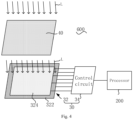
- the electronic device 1000 further includes a different camera assembly 600.
- the different camera assembly 600 includes an image sensor 30.
- the image sensor 30 includes a pixel array 32 and a control circuit 34.
- the pixel array 30 includes a light sensing region 322 and an imaging region 324.
- the control circuit 34 is configured to control the light sensing region 322 to detect an illumination intensity when a light sensing instruction is received, and to control the imaging region 324 to acquire an image when an imaging instruction is received.
- FIG. 5 there is a single camera assembly 100 configured as the front camera assembly 100a.
- the different camera assembly 600 is configured as the rear camera assembly 600b.
- FIG. 6 there is a single camera assembly 100 configured as the rear camera assembly 100b.
- the different camera assembly 600 is configured as the front camera assembly 600a.
- the processor 200 can perform comprehensive processing on the illumination intensities detected by the different camera assembly 600 and the camera assembly 100 and the acquired images to acquire a final illumination intensity and a final image.
- the processing ways may be similar to those used by the processor 200 to acquire the final illumination intensity and the final image according to the illumination intensities detected by two camera assemblies 100 and the images acquired by the two camera assemblies 100, which will not be described herein.
- a ratio of an area of the imaging region 1224 to an area of the pixel array 122 is greater than or equal to 0.6, and/or a ratio of an area of light sensing region 1222 to the area of the pixel array 122 is greater than or equal to 0.1.
- the ratio of the area of the imaging region 1224 to the area of tie pixel array 122 may be 0.6, 0.7, 0.77, 0.8, 0.9 or the like.
- the ratio of the area of light sensing region 1222 to the area of the pixel array 122 may be 0.1, 0.2, 0.22, 0.4 or the like. Accordingly, it ensures that the image sensor 12 has a better imaging effect on the basis of having the function of detecting the illumination intensity.
- the two pixel arrays 122 of the two lens assemblies 10 may be the same, or may not be the same.
- the imaging region 1224 is contiguous and located in the middle of the pixel array 122.
- the light sensing region 1222 is located around the imaging region 1224.
- the center of the imaging region 1224 and the center of the pixel array 122 may coincide.
- the imaging region 1224 may adopt a central symmetry structure.
- the light sensing region 1222 may be located at one or more sides of the imaging region 1224.
- the light sensing region 1222 may include a plurality of light sensing sub-regions 1225 having the same area and spaced from each other.
- the illumination intensity detected by the light sensing region 1222 may be obtained by taking illumination intensities detected by all the pixel points in the light sensing region 1222 into account.
- the light sensing region 1222 is decentralized as much as possible. In other words, the light sensing region 1222 is decentralized as a plurality of spaced light sensing sub-regions 1225.
- the plurality of light sensing sub-regions 1225 spaced from each other may extend a detection range of the light sensing region 1222 and may improve an accuracy of detection of the light sensing region 1222. In an embodiment, there are four light sensing sub-regions 1225. The light sensing sub-regions 1225 may have a same area. The plurality of light sensing sub-regions 1225 may be arranged above, under, on the left, right of the imaging region 1224 respectively. The number and positions of the plurality of light sensing sub-regions are not limited herein.
- the plurality of light sensing sub-regions 1225 include a left light sensing sub-region 1226 and a right light sensing sub-region 1227.
- the left light sensing sub-region 1226 is on the left of the imaging region 1224, and the right light sensing sub-region 1227 is on the right of the imaging region 1224.
- the left light sensing sub-region 1226 and the right light sensing sub-region 1227 are arranged symmetrically.
- the left light sensing sub-region 1226 detects a left illumination intensity (the left illumination intensity refers to an illumination intensity detected by the left light sensing sub-region).
- the right light sensing sub-region 1227 detects a right illumination intensity (the right illumination intensity refers to an illumination intensity detected by the right light sensing sub-region).
- the illumination intensity detected by the light sensing region 122 is a mean value of the left illumination intensity and the right illumination intensity.
- the plurality of light sensing sub-regions 1225 include an upper light sensing sub-region 1228 and a lower light sensing sub-region 1229.
- the upper sensing sub-region 1228 is above the imaging region 1224.
- the lower light sensing sub-region 1229 is under the imaging region 1224.
- the upper light sensing sub-region 1228 and the lower light sensing sub-region 1229 are arranged symmetrically.
- the upper light sensing sub-region 1228 detects an upper illumination intensity (the upper illumination intensity refers to an illumination intensity detected by the upper light sensing sub-region).
- the lower light sensing sub-region 1229 detects a lower illumination intensity (the lower illumination intensity refers to an illumination intensity detected by the lower light sensing sub-region).
- the illumination intensity detected by the light sensing region 122 is a mean value of the upper illumination intensity and the lower illumination intensity.
- the plurality of light sensing sub-regions 1225 include a left light sensing sub-region 1226, a right light sensing sub-region 1227, an upper light sensing sub-region 1228 and a lower light sensing sub-region 1229.
- the left light sensing sub-region 1226 and the right light sensing sub-region 1227 are arranged symmetrically, and the upper light sensing sub-region 1228 and the lower light sensing sub-region 1229 are arranged symmetrically.
- the left light sensing sub-region 1226, the right light sensing sub-region 1227, the upper light sensing sub-region 1228 and the lower light sensing sub-region 1229 are centrally symmetric.
- the left light sensing sub-region 1226 detects a left illumination intensity.
- the right light sensing sub-region 1227 detects a right illumination intensity.
- the upper light sensing sub-region 1228 detects an upper illumination intensity.
- the lower light sensing sub-region 1229 detects a lower illumination intensity.
- the illumination intensity detected by the light sensing region 122 is a mean value of the left illumination intensity, the right illumination intensity, the upper illumination intensity and the lower illumination intensity.
- the sub-regions being arranged symmetrically means that the sub-regions are symmetric in area and shape with regard to the imaging region 1224.
- the pixel array 122 is in a shape of a circle or an ellipse.
- the imaging region 1224 is in a shape of an inscribed rectangle of the pixel array 122.
- the light sensing region 1222 includes a region other than the inscribed rectangle of the circle or the ellipse.
- the imaging region 1224 is in the middle of the pixel array 122, which can acquire the image easily.
- the light sensing region 1222 is decentralized.
- the light sensing region 1222 on the left of the imaging region 1224 and the light sensing region 1222 on the right of the imaging region 1224 are symmetric.
- the light sensing region 1222 has the same sensitivity to light change on the left and right of the imaging region 1224.
- the light sensing region 1222 above the imaging region 1224 and the light sensing region 1222 under the imaging region 1224 are symmetric.
- the light sensing region 1222 has the same sensitivity to light change above and under the imaging region 1224.
- the light sensing region 1222 can obtain an accurate detection result.
- the pixel array is in a shape of rectangle.
- the imaging region 1224 is in a shape of an inscribed circle or an inscribed ellipse of the rectangle.
- the light sensing region 1222 includes a region other than the inscribed circle or the inscribed ellipse of the rectangle.
- the imaging region 1224 is in the shape of the circle or ellipse.
- the user can obtain an image in the shape of circle or ellipse via the imaging region 1224 without further post-processing, thus satisfying the user's personalized demand.
- the light sensing region 1222 is decentralized, such that the accuracy of the illumination intensity detected by the light sensing region 1222 can be improved.
- the imaging region 1224 is in the middle of the pixel array 122, which can acquire the image easily.
- the light sensing region 1222 above the imaging region 1224 and the light sensing region 1222 under the imaging region 1224 are symmetric.
- the light sensing region 1222 on the left of the imaging region 1224 and the light sensing region 1222 on the right of the imaging region 1224 are symmetric.
- the imaging region 1224 is contiguous and the light sensing region 1222 is contiguous.
- the imaging region 1224 and the light sensing region 1222 share a common boundary.
- Two imaging regions 1224 of the two lens assemblies 10 are located between two light sensing regions 1222 of the two lens assemblies 10.
- the pixel array 122 has a simple structure.
- the control circuit 124 may easily find the pixels in the corresponding imaging region 1224 or the corresponding light sensing region 1222 after receiving the light sensing instruction or the imaging instruction.
- the ratio of the area of the imaging region 1224 to the area of the pixel array 122 is 0.8.
- the ratio of the area of the light sensing region 1222 to the area of the pixel array 122 is 0.2.
- the imaging region 1224 may be in the shape of a rectangle, such that the imaging region 124 may obtain an image in the shape of the rectangle.
- the light sensing region 1222 may also be in the shape of a rectangle, and a long edge of the light sensing region 1222 may intersect a long edge of the imaging region 1224 or a short edge of the imaging region 1224.
- Two imaging regions 1224 of the two lens assemblies 10 are arranged between two light sensing regions 1222 of the two lens assemblies 10.
- one light sensing region 1222 is arranged on the left of a left image sensor 12 and the other light sensing region 1222 is arranged on the right of a right image sensor 12.
- one light sensing region 1222 is arranged above an upper image sensor 12 and the other light sensing region 1222 is arranged under a lower image sensor 12. In this way, the two light sensing regions 1222 of the camera assembly 10 can detect in wide range and obtain more accurate detection result.
- the arrangement of the pixel array 122 of the image sensor 12 may be also suitable to the arrangement of the pixel array 32 of the image sensor 30, which will be not described herein.
- the different camera assembly 600 further includes a filter 40. Light passing through the filter 40 reaches the imaging region 324 of the image sensor 30.
Description
- The present disclosure relates to electronic devices, and more particularly to a camera assembly, and a mobile electronic device.
- Typically, a front camera can be set on a phone to capture a selfie, while a light sensor can be set to adjust display brightness of a screen of the phone according to ambient brightness. However, when both the front camera and the light sensor are set on the phone, a large space would be occupied by them, such that the space for locating the display screen in the phone decreases, thus leading to a low screen-to-body ratio.
-
US2012092541A1 discloses a method and apparatus for ambient light measurement system. The apparatus includes a display and a combined camera and ambient light measurement arrangement having photosensitive elements. The arrangement is configured to operate in a first power mode and a second different power mode. -
US2012176533A1 discloses an imaging device including a fixed focused lens, an image sensor having an image matrix of a plurality of pixels arranged on a semiconductor substrate and supplying image data, and electronic means for reading the image matrix. -
US2016037070A1 discloses a multi-mode power-effective light and gesture sensing in image sensors, the image sensor includes a read-out integrated circuit, a plurality of pixel electrodes, an optically sensitive layer, and a top electrical contact. In a first low-power mode, electrical current passing through the top electrical contact is configured to be sensed, and independent currents passing through the plurality of pixel electrodes are configured not to be sensed independently. -
US9497367B1 -
US2015046505A1 discloses an information processing method and electronic device, comprising: acquiring a first value of a first parameter by the first sensor; acquiring a second value of the first parameter by the second sensor; judging whether a difference value between the first value and the second value is larger than or equal to a first threshold or not. -
US2013076712A1 discloses distributed light sensors for ambient light detection, in which, when a touch sensor signal indicates that an external object is covering one of the ambient light sensors, data from that ambient light sensor can be discarded. The ambient light sensors may include a primary ambient light sensor such as a human-eye-response ambient light sensor and may include an array of secondary ambient light sensors such as non-human-eye-response sensors. -
US2015092066 discloses using a second camera to adjust settings of a first camera. - Embodiments of the present disclosure provide a camera assembly and a mobile electronic device.
- The camera assembly according to the invention is set out in
independent claim 1. - The mobile electronic device according the invention is defined in claim 3.
- Preferred embodiments of the invention are set out in the dependent claims.
- Additional aspects and advantages of embodiments of present disclosure will be given in part in the following descriptions, become apparent in part from the following descriptions, or be learned from the practice of the embodiments of the present disclosure.
- These and other aspects and advantages of embodiments of the present disclosure will become apparent and more readily appreciated from the following descriptions made with reference to the drawings.
-
Fig. 1 is a schematic diagram of a camera assembly according to an embodiment of the present disclosure. -
Fig. 2 is a schematic stereogram of an electronic device according to an embodiment of the present disclosure. -
Fig. 3 is a front view and a back view of an electronic device according to an embodiment of the present disclosure. -
Fig. 4 is a schematic diagram of a different camera assembly according to an embodiment of the present disclosure. -
Fig. 5 is a front view and a back view of an electronic device according to an embodiment of the present disclosure. -
Fig. 6 is a front view and a back view of an electronic device according to an embodiment of the present disclosure. -
Fig. 7 is a schematic diagram of a pixel array according to an embodiment of the present disclosure. -
Fig. 8 is a schematic diagram of a pixel array according to an embodiment of the present disclosure. -
Fig. 9 is a schematic diagram of a pixel array according to an embodiment of the present disclosure. -
Fig. 10 is a schematic diagram of a pixel array according to an embodiment of the present disclosure. -
Fig. 11 is a schematic diagram of a pixel array according to an embodiment of the present disclosure. -
Fig. 12 is a schematic diagram of a pixel array according to an embodiment of the present disclosure. -
Fig. 13 is a schematic diagram of a pixel array according to an embodiment of the present disclosure. -
Fig. 14 is a schematic diagram of a pixel array according to an embodiment of the invention. -
Fig. 15 is a schematic diagram of a pixel array according to an embodiment of the invention. - Reference will now be made in detail to exemplary embodiments, examples of which are illustrated in the accompanying drawings, in which the same or similar reference numbers throughout the drawings represent the same or similar elements or elements having same or similar functions. Embodiments described below with reference to drawings are merely exemplary and used for explaining the present disclosure, and should not be understood as limitation to the present disclosure.
- In the present disclosure, unless specified or limited otherwise, a structure in which a first feature is "on" a second feature may include an embodiment in which the first feature directly contacts the second feature, and may also include an embodiment in which the first feature indirectly contacts the second feature via an intermediate medium. Moreover, a structure in which a first feature is "on", "over" or "above" a second feature may indicate that the first feature is right above the second feature or obliquely above the second feature, or just indicate that a horizontal level of the first feature is higher than the second feature. A structure in which a first feature is "below", or "under" a second feature may indicate that the first feature is right under the second feature or obliquely under the second feature, or just indicate that a horizontal level of the first feature is lower than the second feature.
- Referring to
Fig. 1 andFig. 2 , thecamera assembly 100 according to embodiments of the present disclosure includes twolens assemblies 10. Eachlens assembly 10 includes animage sensor 12. Eachimage sensor 12 includes apixel array 122 and acontrol circuit 124. - The
pixel array 122 includes alight sensing region 1222 and animaging region 1224. Thecontrol circuit 124 is configured to control thelight sensing region 1222 to detect an illumination intensity when a light sensing instruction is received. Thecontrol circuit 124 is further configured to control theimaging region 1224 to obtain an image when an imaging instruction is received. - In some embodiments, the
lens assembly 10 further includes afilter 14. Thefilter 14 and theimaging region 1224 are arranged correspondingly. Light would reach theimaging region 1224 after passing through thefilter 14. Thefilter 14 may be anRGB filter 14. TheRGB filter 14 can be arranged in Bayer array to allow light L to pass through thefilter 14 and pass through theimaging region 1224, so as to obtain a color image. Further, in some embodiments, thelens assembly 10 may further include a visible filter. The visible filter and thelight sensing region 1222 are arranged correspondingly to allow light L to pass through the visible filter and to reach thelight sensing region 1222. In this way, after the light L passes through the visible filter, visible light of the light L can reach thelight sensing region 1222, such that thelight sensing region 1222 can detect the illumination intensity of the visible light, thus avoiding interference of invisible light such as infrared light, ultraviolet light or the like in the light L. - The
camera assembly 100 according to embodiments of the present disclosure can be applied in anelectronic device 1000 according to embodiments of the present disclosure. Theelectronic device 1000 further includes aprocessor 200. Theprocessor 200 is configured to generate the light sensing instruction and the imaging instruction. In some embodiments, theelectronic device 1000 further includes adisplay screen 300. Thedisplay screen 300 is configured to display data information such as video, image, text, icon and the like. - In the
camera assembly 100 and theelectronic device 1000 mentioned above, thecontrol circuit 124 can realize both detection of the illumination intensity and acquisition of the image by controlling thepixel array 122. In this way, it is unnecessary to set both a camera component and a light sensor component, such that the number of components is reduced, a ratio of space for locating thedisplay screen 300 can be increased, thus increasing the screen-to-body ratio of theelectronic device 1000. - In some embodiments, two
lens assemblies 10 include a main lens assembly and a secondary lens assembly. An area of the imaging region of the main lens assembly is larger than an area of the imaging region of the secondary lens assembly, such that the main lens assembly can realize a better imaging quality. Further, an area of thepixel array 122 of the main lens assembly can be the same as or be different from an area of thepixel array 122 of secondary lens assembly. - The
electronic device 1000 may be a cell phone, a tablet computer, a smart watch or the like. Theelectronic device 1000 according to embodiments of the present will be explained by taking a cell phone as an example. The illumination intensity detected by thecamera assembly 100 can be considered as the basis for adjusting display brightness of thedisplay screen 300 of theelectronic device 1000. For example, when the illumination intensity is high, the display brightness of thedisplay screen 300 can be increased. When the illumination intensity is changed from a high value to a value less than a certain threshold, it can be determined that a user is answering the phone, such that thedisplay screen 300 can be turned off. The image obtained by thecamera assembly 10 can be displayed on thedisplay screen 300, or stored in storage medium of theelectronic device 1000 for reading or transmitting. - The
camera assembly 100 together with thedisplay screen 300 can be set on afront face 400 of theelectronic device 1000. Thecamera assembly 100 can also be disposed on aback face 500 or side face of theelectronic device 1000. The twolens assemblies 10 of thecamera assembly 100 can be arranged laterally or longitudinally. - The
processor 200 is configured to generate the light sensing instruction and the imaging instruction. Further, theprocessor 200 is configured to transmit the light sensing instruction and the imaging instruction to thecontrol circuit 124. In some embodiments, theprocessor 200 can separately generate and transmit the light sensing instruction, or separately generate and transmit the imaging instruction, or simultaneously generate and transmit the light sensing instruction and the imaging instruction. The light sensing instruction and the imaging instruction can be generated by theprocessor 200 when receiving an input operation. The input operation can be an operation inputted by the user or by an application environment. For example, in the cell phone according to embodiments of the present disclosure, the light sensing instruction and the imaging instruction can be generated by theprocessor 200 after receiving an operation of touching the cell phone or pressing a certain function key (including a physical key, a virtual key) from the user. In some embodiments, the light sensing instruction and the imaging instruction can be generated by theprocessor 200 when the system time of the cell phone reaches a predetermined time point. - A
single control circuit 124 can receive the light sensing instruction and the imaging instruction simultaneously. In other words, thecontrol circuit 124 can simultaneously control thelight sensing region 1222 to detect the illumination intensity and control theimaging region 1224 to acquire the image. Certainly, thecontrol circuit 124 can also be configured to separately receive the light sensing instruction to control thelight sensing region 1222 to detect the illumination intensity, or separately receive the imaging instruction to control theimaging region 1224 to acquire the image. When thecontrol circuit 124 does not receive the light sensing instruction and the imaging instruction, thelight sensing region 1222 and theimaging region 1224 may be in the non-operating state. - The two
control circuits 124 may receive the light sensing instruction and the imaging instruction separately. Thecamera assembly 100 may generate two light sensing instructions and two imaging instructions, which may be a first light sensing instruction, a second light sensing instruction, a first imaging instruction and a second imaging instruction. The first light sensing instruction may be sent only to afirst control circuit 124, but not to asecond control circuit 124. The second light sensing instruction may be sent only to thesecond control circuit 124, but not to thefirst control circuit 124. Similarly, the first imaging instruction may be sent only to thefirst control circuit 124, but not to thesecond control circuit 124. The second imaging instruction may be sent only to thesecond control circuit 124, but not to thefirst control circuit 124. The twocontrol circuits 124 may receive the light sensing instruction and the imaging instruction simultaneously. For example, thecamera assembly 100 may generate a light sensing instruction and an imaging instruction. The light sensing instruction is sent to thefirst control circuit 124 and thesecond control circuit 124 simultaneously. In other words, one light sensing instruction may be used to control twolight sensing regions 1222 to detect the illumination intensity. Similarly, the imaging instruction is sent to thefirst control circuit 124 and the second control circuit simultaneously. In other words, one imaging instruction may be used to control twoimaging regions 1224 to acquire images. - In some embodiments, the
pixel array 122 includes a plurality of pixels arranged in an array. The pixels in thelight sensing region 1222 are configured to detect the illumination intensity. The pixels in theimaging region 1224 are configured to acquire the image. Each pixel can generate corresponding electric quantity according to the illumination intensity of light reaching the pixel. Thecontrol circuit 124 is electrically connected to each pixel. Thecontrol circuit 124 acquires the electric quantity generated by the corresponding pixel according to the received light sensing instruction or imaging instruction, and further analyzes magnitude of the electric quantity via theprocessor 200 to obtain the illumination intensity of the light reaching the corresponding pixel or further performs comprehensive analysis on the illumination intensities of light reaching several pixels via theprocessor 200 to obtain the image. - Referring
Fig. 2 again, in some embodiments, there is asingle camera assembly 100. Thesingle camera assembly 100 is configured as afront camera assembly 100a. Whenlight sensing sensors 1222 of twoimaging sensors 12 detect a first illumination intensity and a second illumination intensity respectively, theprocessor 200 is configured to select a maximum of the first illumination intensity and the second illumination intensity as a final illumination intensity; or theprocessor 200 is configured to obtain a mean value of the first illumination intensity and the second illumination intensity as the final illumination intensity. - The
front camera assembly 100a and thedisplay screen 300 are disposed on thefront face 400 of theelectronic device 1000. Thefront camera assembly 100a may be configured to detect the illumination intensity on thefront face 400 and acquire the image opposite to thefront face 400 simultaneously. - In this way, the
processor 200 can obtain the final illumination intensity after perform the comprehensive analysis on the first illumination intensity and the second illumination intensity respectively obtained by twolight sensing regions 1222. Theelectronic device 1000 further performs corresponding control according to the final illumination intensity, for example adjusting the display brightness of thedisplay screen 300. In some embodiments, during the usage, there may be a situation that twolens assemblies 10 receive very different illumination intensities. For example, when the user operates theelectronic device 1000 under the shade of a tree, onelens assembly 10 may be in the shade while theother lens assembly 10 may be exposed under direct sunlight, such that there may be large difference between the first illumination intensity and the second illumination intensity detected by twolight sensing regions 1222. Theprocessor 200 processes the first illumination intensity and the second illumination intensity to obtain the final illumination intensity and adjusts the display brightness of thedisplay screen 300 according to the final illumination intensity, thus preventing the display brightness from being too high or too low. - Further, the two
lens assemblies 10 in thefront camera assembly 100a may realize imaging simultaneously or on time-sharing. - Working or not working of each of the two
light sensing regions 1222 and the twoimaging regions 1224 in thefront camera assembly 100a is independent of the others. The operating state of thefront camera assembly 100a may be represented by a combination indicating whether each of the twolight sensing regions 1222 and the twoimaging regions 1224 is working or not. As illustrated in table 1, if an indication "√" is used for alight sensing region 1222 or animaging region 1224, it means that thelight sensing region 1222 or theimaging region 1224 is working. If an indication "×" is used for alight sensing region 1222 or animaging region 1224, it means that thelight sensing region 1222 or theimaging region 1224 is not working.Table 1 No. Front camera assembly Image sensor 1 Image sensor 2 Light sensing region Imaging region Light sensing region Imaging region 1 √ × × × 2 √ √ × × 3 √ × × √ 4 √ √ × √ 5 √ × √ × 6 √ √ √ × 7 √ √ √ √ 8 × √ × × 9 × √ × √ - In one embodiment, the two
lens assemblies 10 in thefront camera assembly 100a can realize imaging simultaneously to optimize the imaging quality. For example, the twolens assemblies 10 in thefront camera assembly 100a can realize imaging simultaneously to obtain multiple frames of first images and multiple frames of second images. Theprocessor 200 may analyze the multiple frames of first images and the multiple frames of second images and screens out a frame of image with highest imaging quality as a final image. In another embodiment, theprocessor 200 may perform merging and splicing processing on the first image and the second image to enhance color and definition of the final image. - According to the invention, one
lens assembly 10 in thefront camera assembly 100a may be configured to assist theother lens assembly 10 in imaging, so as to optimize the imaging quality. For example, the onelens assembly 10 in thefront camera assembly 100a may detect the current ambient brightness, and theprocessor 200 analyzes the ambient brightness to control exposure time of each light sensor component corresponding to each pixel in theother lens assembly 10 to obtain the image with suitable brightness. In this way, during the imaging of thecamera assembly 100, onelens assembly 10 is used to detect the ambient brightness to assist theother lens assembly 10 in imaging, such that problems that the final image is subject to overexposure or has too low brightness can be avoided, thus improving the image quality. - In a further embodiment, the two
lens assemblies 10 in thefront camera assembly 100a may be enabled in sequence to realize imaging so as to optimize the imaging quality. For example, onelens assembly 10 in thefront camera assembly 100a adopts a wide-angle lens, while theother lens assembly 10 adopts a telephoto lens. When thecamera assembly 100 realizes imaging, theprocessor 200 enables thelens assembly 10 using the wide-angle lens to realize imaging. If theelectronic device 1000 detects that the user takes a scaling-up operation for a preview image and theprocessor 200 derives an enlarging scale of the preview image higher than a predetermined value, theprocessor 200 immediately enables thelens assembly 10 using the telephoto lens to realize imaging. The wide-angle lens has a big field of view and a short focal length, while the telephoto lens has a small field of view and a long focal length. When the user takes the scaling-up operation for the preview image, it indicates that the user would like to take a picture of distant view, in this case, it needs to adopt the telephoto lens to get a clear picture of the distant view, thus it needs to switch thecamera assembly 100 to thelens assembly 10 using the telephoto lens to realize imaging so as to improve the definition of the image. - However, in some usage scenario of the
electronic device 1000, there may be a situation that the illumination intensities on thefront face 400 and theback face 500 of theelectronic device 1000 are different obviously. For example, the user may put the electronic device 1000 (e.g. a cell phone) on the table with thefront face 400 opposite to the table top. If the display brightness of thedisplay screen 300 is controlled only according to the illumination intensity on thefront face 400 detected by thefront camera assembly 100a, thedisplay screen 300 may be in a non-display state or in a low-brightness-display state. When the user suddenly picks up theelectronic device 1000 for using, theelectronic device 1000 needs to awaken thedisplay screen 300 or to increase the brightness of thedisplay screen 300 in a short time. When the user frequently picks up and puts down theelectronic device 1000, theelectronic device 1000 would consume a great quantity of electricity energy for controlling the brightness of thedisplay screen 300. For another example, if the user operates theelectronic device 1000 when he/she lies down indoor, theback face 500 may be opposite to a light source (such as a ceiling lamp) amounted on the ceiling, such that the illumination intensity on theback face 500 may be greater than that on thefront face 400. In this case, if the brightness of thedisplay screen 300 is adjusted only according to the illumination intensity on thefront face 400, it is possible that the user cannot make out the displayed content due to the low brightness. Thus, if theprocessor 200 can process both the illumination intensity on thefront face 400 and the illumination intensity on theback face 500 of theelectronic device 1000, an optimum illumination intensity can be obtained. - Referring to
Fig. 3 , in some embodiments, there are a plurality ofcamera assemblies 100. One of them is configured as afront camera assembly 100a, a further of them is configured as arear camera assembly 100b. Thefront camera assembly 100a and thedisplay screen 300 are disposed on thefront face 400 of theelectronic device 1000. Thefront camera assembly 100a may be configured to detect the illumination intensity on thefront face 400 and acquire the image opposite to thefront face 400 simultaneously. Therear camera assembly 100b is disposed on theback face 500 of theelectronic device 1000. Therear camera assembly 100b may be configured to detect the illumination intensity on theback face 500 and acquire the image opposite to theback face 500 simultaneously. - Working or not working of each of four
light sensing regions 1222 and fourimaging regions 1224 in thefront camera assembly 100a and therear camera assembly 100b is independent of the others. The operating state of thefront camera assembly 100a may be represented by a combination indicating whether each of thelight sensing regions 1222 andimaging regions 1224 in thefront camera assembly 100a is working or not. The operating state of therear camera assembly 100b may be represented by a combination indicating whether each of thelight sensing regions 1222 andimaging regions 1224 in therear camera assembly 100b is working or not. As illustrated in table 2, if an indication "√" is used for alight sensing region 1222 or animaging region 1224, it means that thelight sensing region 1222 or theimaging region 1224 is working. If an indication "×" is used for alight sensing region 1222 or animaging region 1224, it means that thelight sensing region 1222 or theimaging region 1224 is not working. However, the operating state of thefront camera assembly 100a and the operating state of therear camera assembly 100b are not limited in the following table, there may be other operating states, which are not listed herein.Table 2 No. Front camera assembly Rear camera assembly Image sensor 1 Image sensor 2 Image sensor 3 Image sensor 4 Light sensing region Imaging region Light sensing region Imaging region Light sensing region Imaging region Light sensing region Imaging region 1 √ × √ × √ × √ × 2 √ × √ × √ × × × 3 √ × × × √ × √ × 4 √ × × × √ × × × 5 √ √ √ × √ × √ √ 6 √ √ × × √ √ √ √ 7 √ √ × √ √ × × × ⋮ ⋮ ⋮ ⋮ ⋮ ⋮ ⋮ ⋮ ⋮ - In some operating states, for example, in the operating state No. 1, two
light sensing regions 1222 in thefront camera assembly 100a detect a first illumination intensity and a second illumination intensity respectively, and twolight sensing regions 1222 in therear camera assembly 100b detect a third illumination intensity and a fourth illumination intensity respectively. In this case, the final illumination intensity of theelectronic device 1000 can be calculated based on one of the following four ways. - Way one, the
processor 200 may be configured to select a maximum of the first illumination intensity, the second illumination intensity, the third illumination intensity and the fourth illumination intensity as the final illumination intensity. - Way two, the
processor 200 may be configured to obtain a mean value of the first illumination intensity and the second illumination intensity as a front illumination intensity (the front illumination intensity refers to an illumination intensity detected by the light sensing region in the front camera assembly), to obtain a mean value of the third illumination intensity and the fourth illumination intensity as a rear illumination intensity (the rear illumination intensity refers to an illumination intensity detected by the light sensing region in the rear camera assembly), and to select a maximum of the front illumination intensity and the rear illumination intensity as the final illumination intensity. - Way three, the
processor 200 may be configured to select a maximum of the first illumination intensity and the second illumination intensity as the front illumination intensity, to obtain a mean value of the third illumination intensity and the fourth illumination intensity as the rear illumination intensity, and to select a maximum of the front illumination intensity and the rear illumination intensity as the final illumination intensity. - Way four, the
processor 200 may be configured to obtain a mean value of the first illumination intensity and the second illumination intensity as the front illumination intensity, to select a maximum of the third illumination intensity and the fourth illumination intensity as the rear illumination intensity, and to select a maximum of the front illumination intensity and the rear illumination intensity as the final illumination intensity. - In some embodiments, the
processor 200 can switch the calculation way among the above four ways, which can be realized by the user manually or automatically according to specific values of the illumination intensities. For example, when each of the first illumination intensity, the second illumination intensity, the third illumination intensity and the fourth illumination intensity is less than a predetermined illumination intensity threshold, it may be determined that the user may use theelectronic device 1000 in a dark environment, thus theprocessor 200 can switch the calculation way to way one, i.e., selecting the maximum as the final illumination intensity. - To this, all of the four
light sensing regions 1222 in thefront camera assembly 100a and therear camera assembly 100b are configured to detect illumination intensities, and the final illumination intensity obtained by theprocessor 200 can reflect the actual illumination intensity of the environment objectively. - In some operating states, for example, in the operating state No. 4 of table 2, one
light sensing region 1222 in thefront camera assembly 100a detects a first illumination intensity, onelight sensing region 1222 in therear camera assembly 100b detects a second illumination intensity. Theprocessor 200 is configured to select a maximum of the first illumination intensity and the second illumination intensity as the final illumination intensity. - To this, each of the
front camera assembly 100a and therear camera assembly 100b enables onelight sensing region 1222 when working to save energy. When onelight sensing region 1222 in thefront camera assembly 100a breaks down, the otherlight sensing region 1222 in thefront camera assembly 100a can be used to detect the first illumination intensity. When onelight sensing region 1222 in therear camera assembly 100b breaks down, the otherlight sensing region 1222 in therear camera assembly 100b can be used to detect the second illumination intensity. Thus, the normal use of theelectronic device 1000 will be not affected. - In some operating states, for example, in the operating state No. 2 of table 2, two
light sensing regions 1222 in thefront camera assembly 100a detect a first illumination intensity and a second illumination intensity respectively, and onelight sensing region 1222 in therear camera assembly 100b detects a third illumination intensity. In this way, the final illumination intensity of theelectronic device 1000 can be calculated based on one of the following two ways. - Way one, the
processor 200 is configured to select a maximum of the first illumination intensity and the second illumination intensity as the front illumination intensity, and to select a maximum of the front illumination intensity and the third illumination intensity as the final illumination intensity. - Way two, the
processor 200 is configured to obtain a mean value of the first illumination intensity and the second illumination intensity as the front illumination intensity, and to select a maximum of the front illumination intensity and the third illumination intensity as the final illumination intensity. - In some embodiments, the
processor 200 can switch the calculation way between the above two ways. Therear camera assembly 100b only enables onelight sensing region 1222 when working, to save energy. When onelight sensing region 1222 in therear camera assembly 100b breaks down, the otherlight sensing region 1222 in therear camera assembly 100b can be used to detect the third illumination intensity. Thus, the normal use of theelectronic device 1000 will be not affected. - In some operating states, for example, in the operating state No. 3 of table 2, one
light sensing region 1222 in thefront camera assembly 100a detects a first illumination intensity, and twolight sensing regions 1222 in therear camera assembly 100b detect a second illumination intensity and a third illumination intensity respectively. In this way, the final illumination intensity of theelectronic device 1000 can be calculated based on one of the following two ways. - Way one, the
processor 200 is configured to select a maximum of the second illumination intensity and the third illumination intensity as the rear illumination intensity, and to select a maximum of the rear illumination intensity and the first illumination intensity as the final illumination intensity. - Way two, the
processor 200 is configured to obtain a mean value of the second illumination intensity and the third illumination intensity as the rear illumination intensity, and to select a maximum of the rear illumination intensity and the first illumination intensity as the final illumination intensity. - In some embodiments, the
processor 200 can switch the calculation way between the above two ways. Thefront camera assembly 100a only enables onelight sensing region 1222 when working, to save energy. When onelight sensing region 1222 in thefront camera assembly 100a breaks down, the otherlight sensing region 1222 in thefront camera assembly 100a can be used to detect the first illumination intensity. Thus, the normal use of theelectronic device 1000 will be not affected. - Further, the
front camera assembly 100a and therear camera assembly 100b can realize imaging simultaneously or on time-sharing. - In one embodiment, the
front camera assembly 100a and therear camera assembly 100b can realize imaging simultaneously. For example, theprocessor 200 enables both thefront camera assembly 100a and therear camera assembly 100b. Therear camera assembly 100b is configured to take a picture of the scenery behind theelectronic device 1000. Thefront camera assembly 100a is configured to take a picture of face of the user. Thedisplay screen 300 of theelectronic device 1000 displays the images captured by both thefront camera assembly 100a and therear camera assembly 100b simultaneously. Further, theprocessor 200 may store the images captured at the same time by both thefront camera assembly 100a and therear camera assembly 100b in association with each other. When the user browses the stored images, both the scenery and the face of the user who enjoys the scenery can be checked, thus improving the user experience. - In another embodiment, the
front camera assembly 100a and therear camera assembly 100b may realize imaging on time-sharing. For example, thefront camera assembly 100a is working while therear camera assembly 100b is disabled, or thefront camera assembly 100a is disabled but therear camera assembly 100b is working. In this way, theelectronic device 1000 not only can take a picture of the scenery behind theelectronic device 1000 but also can capture the selfie. - The two
lens assemblies 10 in thefront camera assembly 100a may realize imaging simultaneously or on time-sharing to optimize the imaging quality. The twolens assemblies 10 in therear camera assembly 100b may also realize imaging simultaneously or on time-sharing to optimize the imaging quality, which will not be described herein. - Referring to
Figs. 4-6 , in some embodiments, theelectronic device 1000 further includes adifferent camera assembly 600. Thedifferent camera assembly 600 includes animage sensor 30. Theimage sensor 30 includes apixel array 32 and acontrol circuit 34. Thepixel array 30 includes alight sensing region 322 and animaging region 324. Thecontrol circuit 34 is configured to control thelight sensing region 322 to detect an illumination intensity when a light sensing instruction is received, and to control theimaging region 324 to acquire an image when an imaging instruction is received. - Referring to
Fig. 5 , in some embodiments, there is asingle camera assembly 100 configured as thefront camera assembly 100a. Thedifferent camera assembly 600 is configured as therear camera assembly 600b. - Referring to
Fig. 6 , in some embodiments, there is asingle camera assembly 100 configured as therear camera assembly 100b. Thedifferent camera assembly 600 is configured as thefront camera assembly 600a. - The
processor 200 can perform comprehensive processing on the illumination intensities detected by thedifferent camera assembly 600 and thecamera assembly 100 and the acquired images to acquire a final illumination intensity and a final image. The processing ways may be similar to those used by theprocessor 200 to acquire the final illumination intensity and the final image according to the illumination intensities detected by twocamera assemblies 100 and the images acquired by the twocamera assemblies 100, which will not be described herein. - In some embodiments, a ratio of an area of the
imaging region 1224 to an area of thepixel array 122 is greater than or equal to 0.6, and/or a ratio of an area oflight sensing region 1222 to the area of thepixel array 122 is greater than or equal to 0.1. In some embodiments, the ratio of the area of theimaging region 1224 to the area oftie pixel array 122 may be 0.6, 0.7, 0.77, 0.8, 0.9 or the like. The ratio of the area oflight sensing region 1222 to the area of thepixel array 122 may be 0.1, 0.2, 0.22, 0.4 or the like. Accordingly, it ensures that theimage sensor 12 has a better imaging effect on the basis of having the function of detecting the illumination intensity. - In some embodiments, the two
pixel arrays 122 of the twolens assemblies 10 may be the same, or may not be the same. - Referring to
Figs. 7 and8 , in some embodiments, theimaging region 1224 is contiguous and located in the middle of thepixel array 122. Thelight sensing region 1222 is located around theimaging region 1224. Thus, it is easy for thecontiguous imaging region 1224 to generate a continuous and complete image. In some embodiments, the center of theimaging region 1224 and the center of thepixel array 122 may coincide. Theimaging region 1224 may adopt a central symmetry structure. Thelight sensing region 1222 may be located at one or more sides of theimaging region 1224. - In some embodiments, the
light sensing region 1222 may include a plurality oflight sensing sub-regions 1225 having the same area and spaced from each other. - The illumination intensity detected by the
light sensing region 1222 may be obtained by taking illumination intensities detected by all the pixel points in thelight sensing region 1222 into account. Thus, in order to obtain an objective illumination intensity, thelight sensing region 1222 is decentralized as much as possible. In other words, thelight sensing region 1222 is decentralized as a plurality of spacedlight sensing sub-regions 1225. - The plurality of
light sensing sub-regions 1225 spaced from each other may extend a detection range of thelight sensing region 1222 and may improve an accuracy of detection of thelight sensing region 1222. In an embodiment, there are fourlight sensing sub-regions 1225. Thelight sensing sub-regions 1225 may have a same area. The plurality oflight sensing sub-regions 1225 may be arranged above, under, on the left, right of theimaging region 1224 respectively. The number and positions of the plurality of light sensing sub-regions are not limited herein. - Referring to
Fig. 9 , in some embodiments, the plurality oflight sensing sub-regions 1225 include a leftlight sensing sub-region 1226 and a rightlight sensing sub-region 1227. The leftlight sensing sub-region 1226 is on the left of theimaging region 1224, and the rightlight sensing sub-region 1227 is on the right of theimaging region 1224. The leftlight sensing sub-region 1226 and the rightlight sensing sub-region 1227 are arranged symmetrically. The leftlight sensing sub-region 1226 detects a left illumination intensity (the left illumination intensity refers to an illumination intensity detected by the left light sensing sub-region). The rightlight sensing sub-region 1227 detects a right illumination intensity (the right illumination intensity refers to an illumination intensity detected by the right light sensing sub-region). The illumination intensity detected by thelight sensing region 122 is a mean value of the left illumination intensity and the right illumination intensity. - To this, influences of the left
light sensing sub-region 1226 and the rightlight sensing sub-region 1227 to the illumination intensity detected by thelight sensing region 122 are the same essentially, thus the problem that the detection result is inaccurate because thelight sensing region 122 is too sensitive to light change on the left or right of the imaging region can be avoided. - In some embodiments, the plurality of
light sensing sub-regions 1225 include an upperlight sensing sub-region 1228 and a lowerlight sensing sub-region 1229. Theupper sensing sub-region 1228 is above theimaging region 1224. The lowerlight sensing sub-region 1229 is under theimaging region 1224. The upperlight sensing sub-region 1228 and the lowerlight sensing sub-region 1229 are arranged symmetrically. The upperlight sensing sub-region 1228 detects an upper illumination intensity (the upper illumination intensity refers to an illumination intensity detected by the upper light sensing sub-region). The lowerlight sensing sub-region 1229 detects a lower illumination intensity (the lower illumination intensity refers to an illumination intensity detected by the lower light sensing sub-region). The illumination intensity detected by thelight sensing region 122 is a mean value of the upper illumination intensity and the lower illumination intensity. - To this, influences of the upper
light sensing sub-region 1228 and the lowerlight sensing sub-region 1229 to the illumination intensity detected by thelight sensing region 122 are the same essentially, thus the problem that the detection result is inaccurate because thelight sensing region 122 is too sensitive to light change above or under the imaging region can be avoided. - In some embodiments, the plurality of
light sensing sub-regions 1225 include a leftlight sensing sub-region 1226, a rightlight sensing sub-region 1227, an upperlight sensing sub-region 1228 and a lowerlight sensing sub-region 1229. The leftlight sensing sub-region 1226 and the rightlight sensing sub-region 1227 are arranged symmetrically, and the upperlight sensing sub-region 1228 and the lowerlight sensing sub-region 1229 are arranged symmetrically. In an embodiment, the leftlight sensing sub-region 1226, the rightlight sensing sub-region 1227, the upperlight sensing sub-region 1228 and the lowerlight sensing sub-region 1229 are centrally symmetric. The leftlight sensing sub-region 1226 detects a left illumination intensity. The rightlight sensing sub-region 1227 detects a right illumination intensity. The upperlight sensing sub-region 1228 detects an upper illumination intensity. The lowerlight sensing sub-region 1229 detects a lower illumination intensity. The illumination intensity detected by thelight sensing region 122 is a mean value of the left illumination intensity, the right illumination intensity, the upper illumination intensity and the lower illumination intensity. - To this, influences of the left
light sensing sub-region 1226, the rightlight sensing sub-region 1227, the upperlight sensing sub-region 1228 and the lowerlight sensing sub-region 1229 to the illumination intensity detected by thelight sensing region 122 are the same essentially, thus the problem that the detection result is inaccurate because thelight sensing region 122 is too sensitive to light change above, under, on the left or right of the imaging region can be avoided. - The sub-regions being arranged symmetrically means that the sub-regions are symmetric in area and shape with regard to the
imaging region 1224. - Referring to
Figs. 10 and11 , in some embodiments, thepixel array 122 is in a shape of a circle or an ellipse. Theimaging region 1224 is in a shape of an inscribed rectangle of thepixel array 122. Thelight sensing region 1222 includes a region other than the inscribed rectangle of the circle or the ellipse. - Accordingly, the
imaging region 1224 is in the middle of thepixel array 122, which can acquire the image easily. Thelight sensing region 1222 is decentralized. Thelight sensing region 1222 on the left of theimaging region 1224 and thelight sensing region 1222 on the right of theimaging region 1224 are symmetric. Thelight sensing region 1222 has the same sensitivity to light change on the left and right of theimaging region 1224. Thelight sensing region 1222 above theimaging region 1224 and thelight sensing region 1222 under theimaging region 1224 are symmetric. Thelight sensing region 1222 has the same sensitivity to light change above and under theimaging region 1224. Thus, thelight sensing region 1222 can obtain an accurate detection result. - Referring to
Figs. 12 and 13 , the pixel array is in a shape of rectangle. Theimaging region 1224 is in a shape of an inscribed circle or an inscribed ellipse of the rectangle. Thelight sensing region 1222 includes a region other than the inscribed circle or the inscribed ellipse of the rectangle. - Accordingly, the
imaging region 1224 is in the shape of the circle or ellipse. The user can obtain an image in the shape of circle or ellipse via theimaging region 1224 without further post-processing, thus satisfying the user's personalized demand. Thelight sensing region 1222 is decentralized, such that the accuracy of the illumination intensity detected by thelight sensing region 1222 can be improved. - Thus, the
imaging region 1224 is in the middle of thepixel array 122, which can acquire the image easily. Thelight sensing region 1222 above theimaging region 1224 and thelight sensing region 1222 under theimaging region 1224 are symmetric. Thelight sensing region 1222 on the left of theimaging region 1224 and thelight sensing region 1222 on the right of theimaging region 1224 are symmetric. - Referring to
Figs. 14 and 15 , according to the invention, theimaging region 1224 is contiguous and thelight sensing region 1222 is contiguous. Theimaging region 1224 and thelight sensing region 1222 share a common boundary. Twoimaging regions 1224 of the twolens assemblies 10 are located between twolight sensing regions 1222 of the twolens assemblies 10. Thus, thepixel array 122 has a simple structure. Thecontrol circuit 124 may easily find the pixels in the correspondingimaging region 1224 or the correspondinglight sensing region 1222 after receiving the light sensing instruction or the imaging instruction. In some embodiments, the ratio of the area of theimaging region 1224 to the area of thepixel array 122 is 0.8. The ratio of the area of thelight sensing region 1222 to the area of thepixel array 122 is 0.2. Theimaging region 1224 may be in the shape of a rectangle, such that theimaging region 124 may obtain an image in the shape of the rectangle. Thelight sensing region 1222 may also be in the shape of a rectangle, and a long edge of thelight sensing region 1222 may intersect a long edge of theimaging region 1224 or a short edge of theimaging region 1224. - Two
imaging regions 1224 of the twolens assemblies 10 are arranged between twolight sensing regions 1222 of the twolens assemblies 10. In some embodiments, as illustrated inFig. 14 , when the twolens assemblies 10 are arranged laterally, onelight sensing region 1222 is arranged on the left of aleft image sensor 12 and the otherlight sensing region 1222 is arranged on the right of aright image sensor 12. As illustrated inFig. 15 , when the twolens assemblies 10 are arranged longitudinally, onelight sensing region 1222 is arranged above anupper image sensor 12 and the otherlight sensing region 1222 is arranged under alower image sensor 12. In this way, the twolight sensing regions 1222 of thecamera assembly 10 can detect in wide range and obtain more accurate detection result. - The arrangement of the
pixel array 122 of theimage sensor 12 may be also suitable to the arrangement of thepixel array 32 of theimage sensor 30, which will be not described herein. Thedifferent camera assembly 600 further includes afilter 40. Light passing through thefilter 40 reaches theimaging region 324 of theimage sensor 30.
Claims (10)
- A camera assembly (100), configured on a mobile electronic device having a display screen, comprising at least two lens assemblies (10), each lens assembly comprising an image sensor (12), wherein each image sensor (12) comprises:a pixel array (122), comprising a light sensing region (1222) and an imaging region (1224); anda control circuit (124), configured to:control the light sensing region (1222) to detect an illumination intensity so as to adjust a display brightness of the display screen when a light sensing instruction is received; andcontrol the imaging region (1224) to obtain an image when an imaging instruction is received, wherein,the at least two lens assemblies (10) comprise a first lens assembly and a second lens assembly, the first lens assembly is configured to detect an ambient brightness to assist the second lens assembly in imaging during an imaging of the camera assembly (100),wherein the imaging region (1224) of each image sensor (12) is contiguous and the light sensing region (1222) of each image sensor (12) is contiguous; the imaging region (1224) and the light sensing region (1222) of each image sensor (12) share a common boundary, the camera assembly (100) comprises two image sensors, and all of two imaging regions of the two image sensors are located between two light sensing regions of the two image sensors.
- The camera assembly (100) according to claim 1, wherein the pixel array (122) of each image sensor (12) is configured such that at least one of following conditions is satisfied: a ratio of an area of the imaging region (1224) of said image sensor (12) to an area of the pixel array (122) of said image sensor (12) being greater than or equal to 0.6; and a ratio of an area of the light sensing region (1222) of said image sensor (12) to the area of the pixel array (122) of said image sensor (12) being greater than or equal to 0.1; and/or
an area of the imaging region (1224) of one of the at least two image sensors (12) is greater than an area of the imaging region (1224) of a further one of the at least two image sensors (12). - A mobile electronic device (1000), comprising at least one camera assembly (100) according to any of claims 1-2 and a processor (200); wherein,
the processor (200) is configured to generate the light sensing instruction and the imaging instruction. - The mobile electronic device (1000) according to claim 3, wherein the mobile electronic device (1000) comprises one camera assembly (100) configured as a front camera assembly (100a);
wherein when light sensing regions (1222) of at least two image sensors (12) of the camera assembly (100) detect a first illumination intensity and a second illumination intensity respectively, the processor (200) is configured to:determine a maximum of the first illumination intensity and the second illumination intensity as a final illumination intensity; orobtain a mean value of the first illumination intensity and the second illumination intensity as a final illumination intensity. - The mobile electronic device (1000) according to claim 3, wherein the mobile electronic device (1000) comprises at least two camera assemblies (100), one of the at least two camera assemblies (100) is configured as a front camera assembly (100a) and a further one of the at least two camera assemblies (100) is configured as a rear camera assembly (100b);
wherein when two light sensing regions (1222) of the front camera assembly (100a) detect a first illumination intensity and a second illumination intensity respectively, and two light sensing regions (1222) of the rear camera assembly (100b) detect a third illumination intensity and a fourth illumination intensity respectively, the processor (200) is configured to:determine a maximum of the first illumination intensity, the second illumination intensity, the third illumination intensity and the fourth illumination intensity as a final illumination intensity; orobtain a mean value of the first illumination intensity and the second illumination intensity as a front illumination intensity, obtain a mean value of the third illumination intensity and the fourth illumination intensity as a rear illumination intensity, and determine a maximum of the front illumination intensity and the rear illumination intensity as a final illumination intensity; ordetermine a maximum of the first illumination intensity and the second illumination intensity as a front illumination intensity, obtain a mean value of the third illumination intensity and the fourth illumination intensity as a rear illumination intensity, and determine a maximum of the front illumination intensity and the rear illumination intensity as a final illumination intensity; orobtain a mean value of the first illumination intensity and the second illumination intensity as a front illumination intensity, determine a maximum of the third illumination intensity and the fourth illumination intensity as a rear illumination intensity, and determine a maximum of the front illumination intensity and the rear illumination intensity as a final illumination intensity. - The mobile electronic device (1000) according to claim 3, wherein the mobile electronic device (1000) comprises at least two camera assemblies (100), one of the at least two camera assemblies (100) is configured as a front camera assembly (100a) and a further one of the at least two camera assemblies (100) is configured as a rear camera assembly (100b);
wherein when a light sensing region (1222) of the front camera assembly (100a) detects a first illumination intensity, and a light sensing region (1222) of the rear camera assembly (100b) detects a second illumination intensity, the processor (200) is configured to:
determine a maximum of the first illumination intensity and the second illumination intensity as a final illumination intensity. - The mobile electronic device (1000) according to claim 3, wherein the mobile electronic device (1000) comprises at least two camera assemblies (100), one of the at least two camera assemblies (100) is configured as a front camera assembly (100a) and a further one of the at least two camera assemblies (100) is configured as a rear camera assembly (100b);
wherein when two light sensing regions (1222) of the front camera assembly (100a) detect a first illumination intensity and a second illumination intensity respectively, and a light sensing region (1222) of the rear camera assembly (100b) detects a third illumination intensity, the processor (200) is configured to:determine a maximum of the first illumination intensity and the second illumination intensity as a front illumination intensity, and determine a maximum of the front illumination intensity and the third illumination intensity as a final illumination intensity; orobtain a mean value of the first illumination intensity and the second illumination intensity as a front illumination intensity, and determine a maximum of the front illumination intensity and the third illumination intensity as a final illumination intensity. - The mobile electronic device (1000) according to claim 3, wherein the mobile electronic device (1000) comprises at least two camera assemblies (100), one of the at least two camera assemblies (100) is configured as a front camera assembly (100a) and a further one of the at least two camera assemblies (100) is configured as a rear camera assembly (100b);
wherein when a light sensing region (1222) of the front camera assembly (100a) detects a first illumination intensity, and two light sensing regions (1222) of the rear camera assembly (100b) detect a second illumination intensity and a third illumination intensity respectively, the processor (200) is configured to:determine a maximum of the second illumination intensity and the third illumination intensity as a rear illumination intensity, and determine a maximum of the rear illumination intensity and the first illumination intensity as a final illumination intensity; orobtain a mean value of the second illumination intensity and the third illumination intensity as a rear illumination intensity, and determine a maximum of the rear illumination intensity and the first illumination intensity as a final illumination intensity. - The mobile electronic device (1000) according to any of claims 3-8, further comprising another camera assembly (600), wherein the another camera assembly (600) comprises an image sensor (30) comprising:a pixel array (32), comprising a light sensing region (322) and an imaging region (324); anda control circuit (34), configured to:control the light sensing region (322) of the imaging sensor (30) of the another camera assembly (600) to detect an illumination intensity when the light sensing instruction is received; andcontrol the imaging region (324) of the imaging sensor (30) of the another camera assembly (600) to obtain an image when the imaging instruction is received.
- The mobile electronic device (1000) according to claim 9, wherein the mobile electronic device (1000) comprises one camera assembly (100) configured as one of a front camera assembly (100a) and a rear camera assembly (100b), and the said another camera assembly (600) is configured as the other one of the front camera assembly (100a) and the rear camera assembly (100b).
Applications Claiming Priority (1)
| Application Number | Priority Date | Filing Date | Title |
|---|---|---|---|
| CN201710305891.5A CN107426471B (en) | 2017-05-03 | 2017-05-03 | Camera module and electronic device |
Publications (2)
| Publication Number | Publication Date |
|---|---|
| EP3399288A1 EP3399288A1 (en) | 2018-11-07 |
| EP3399288B1 true EP3399288B1 (en) | 2023-04-12 |
Family
ID=60424931
Family Applications (1)
| Application Number | Title | Priority Date | Filing Date |
|---|---|---|---|
| EP18170252.3A Active EP3399288B1 (en) | 2017-05-03 | 2018-05-01 | Camera assembly and mobile electronic device |
Country Status (10)
| Country | Link |
|---|---|
| US (2) | US10412205B2 (en) |
| EP (1) | EP3399288B1 (en) |
| JP (1) | JP7023965B2 (en) |
| KR (1) | KR20190085982A (en) |
| CN (1) | CN107426471B (en) |
| AU (1) | AU2018263022B2 (en) |
| CA (1) | CA3049704C (en) |
| IL (1) | IL268500B (en) |
| SG (1) | SG11201906723WA (en) |
| WO (1) | WO2018202050A1 (en) |
Families Citing this family (10)
| Publication number | Priority date | Publication date | Assignee | Title |
|---|---|---|---|---|
| USD860178S1 (en) * | 2016-11-28 | 2019-09-17 | Samsung Electronics Co., Ltd. | Mobile phone |
| CN107426471B (en) * | 2017-05-03 | 2021-02-05 | Oppo广东移动通信有限公司 | Camera module and electronic device |
| CN107135341B (en) * | 2017-05-03 | 2019-12-27 | Oppo广东移动通信有限公司 | Image sensor, camera module and electronic device |
| CN107222591B (en) * | 2017-05-03 | 2021-02-05 | Oppo广东移动通信有限公司 | Image sensor, camera module and electronic device |
| CN107222664B (en) * | 2017-05-03 | 2020-03-06 | Oppo广东移动通信有限公司 | Camera module and electronic device |
| KR102192809B1 (en) * | 2017-07-07 | 2020-12-18 | 후아웨이 테크놀러지 컴퍼니 리미티드 | Terminal provided with a camera and a method for photographing the same |
| CN111989906B (en) * | 2018-07-16 | 2022-06-17 | Oppo广东移动通信有限公司 | Electronic device |
| CN109547598B (en) * | 2018-11-30 | 2020-06-26 | Oppo广东移动通信有限公司 | Camera module control method and device |
| CN110225262A (en) * | 2019-06-25 | 2019-09-10 | 武汉华星光电半导体显示技术有限公司 | The light compensation method of taking pictures of special-shaped display screen and its front camera |
| CN112346236A (en) * | 2020-11-04 | 2021-02-09 | Oppo广东移动通信有限公司 | Imaging device and electronic apparatus |
Citations (1)
| Publication number | Priority date | Publication date | Assignee | Title |
|---|---|---|---|---|
| US20150092066A1 (en) * | 2013-09-30 | 2015-04-02 | Google Inc. | Using a Second Camera to Adjust Settings of First Camera |
Family Cites Families (36)
| Publication number | Priority date | Publication date | Assignee | Title |
|---|---|---|---|---|
| EP1517553A4 (en) | 2002-07-11 | 2006-01-25 | Seiko Epson Corp | Output image adjustment of image data |
| JP2004350232A (en) | 2003-05-26 | 2004-12-09 | Konica Minolta Opto Inc | Portable electronic device |
| JP2005099265A (en) | 2003-09-24 | 2005-04-14 | Fujinon Corp | Imaging apparatus, imaging method, and range finding method |
| US20060054782A1 (en) | 2004-08-25 | 2006-03-16 | Olsen Richard I | Apparatus for multiple camera devices and method of operating same |
| US20060260808A1 (en) * | 2005-05-20 | 2006-11-23 | Weaver Jim D | Methods of treating particulates and use in subterranean formations |
| US20080151194A1 (en) * | 2006-01-31 | 2008-06-26 | Avner Segev | Method and System for Illumination Adjustment |
| US20080122821A1 (en) | 2006-11-24 | 2008-05-29 | Sony Ericsson Mobile Communications Ab | Luminance control for a display |
| US7812869B2 (en) | 2007-05-11 | 2010-10-12 | Aptina Imaging Corporation | Configurable pixel array system and method |
| JP2010147786A (en) * | 2008-12-18 | 2010-07-01 | Fujifilm Corp | Imaging device and image processing method |
| CN101771816A (en) * | 2008-12-27 | 2010-07-07 | 鸿富锦精密工业(深圳)有限公司 | Portable electronic device and imaging method |
| US20120092541A1 (en) * | 2010-10-19 | 2012-04-19 | Nokia Corporation | Method and apparatus for ambient light measurement system |
| EP2472853A1 (en) * | 2011-01-03 | 2012-07-04 | STMicroelectronics (Grenoble 2) SAS | Imaging device with ambient light sensing means |
| CN102595030A (en) * | 2011-01-12 | 2012-07-18 | 英属开曼群岛商恒景科技股份有限公司 | Digital camera device capable of sensing environment light |
| CN202153766U (en) * | 2011-04-26 | 2012-02-29 | 北京思比科微电子技术股份有限公司 | Image processing device for multiple image sensors |
| US20130076712A1 (en) * | 2011-09-22 | 2013-03-28 | Dong Zheng | Distributed Light Sensors for Ambient Light Detection |
| US9513482B2 (en) * | 2012-06-12 | 2016-12-06 | Intel Corporation | Heads up display systems for glasses |
| JP2014045404A (en) * | 2012-08-28 | 2014-03-13 | Sharp Corp | Portable terminal |
| US9332167B1 (en) * | 2012-11-20 | 2016-05-03 | Amazon Technologies, Inc. | Multi-directional camera module for an electronic device |
| KR101442390B1 (en) | 2013-01-25 | 2014-09-17 | 삼성전기주식회사 | Camera module |
| CN103118231A (en) | 2013-03-07 | 2013-05-22 | 刘烈军 | Image data processing method and related device |
| KR20150014751A (en) * | 2013-07-30 | 2015-02-09 | 삼성전자주식회사 | display apparatus and method thereof |
| US9607571B2 (en) * | 2013-08-07 | 2017-03-28 | Beijing Lenovo Software Ltd. | Information processing method and electronic device |
| JP5931117B2 (en) * | 2014-05-07 | 2016-06-08 | キヤノン株式会社 | Imaging device |
| US10097780B2 (en) * | 2014-06-05 | 2018-10-09 | Invisage Technologies, Inc. | Sensors and systems for the capture of scenes and events in space and time |
| US9692968B2 (en) * | 2014-07-31 | 2017-06-27 | Invisage Technologies, Inc. | Multi-mode power-efficient light and gesture sensing in image sensors |
| CN105472209B (en) * | 2014-09-11 | 2018-12-21 | 比亚迪股份有限公司 | Dual camera systems and electronic device |
| WO2017008013A1 (en) * | 2015-07-09 | 2017-01-12 | Mastercard International Incorporated | Systems and methods for use in authenticating individuals, in connection with providing access to the individuals |
| US9497367B1 (en) * | 2015-07-22 | 2016-11-15 | Ic Real Tech, Inc | Maximizing effective surface area of a rectangular image sensor concurrently capturing image data from two lenses |
| KR102521805B1 (en) * | 2015-11-10 | 2023-04-14 | 삼성전자주식회사 | Camera switching method and electronic device supporting the same |
| KR102524498B1 (en) * | 2016-07-06 | 2023-04-24 | 삼성전자주식회사 | The Electronic Device including the Dual Camera and Method for controlling the Dual Camera |
| TWI622810B (en) * | 2017-04-26 | 2018-05-01 | 和碩聯合科技股份有限公司 | Imaging device and imaging method |
| CN107426471B (en) * | 2017-05-03 | 2021-02-05 | Oppo广东移动通信有限公司 | Camera module and electronic device |
| CN107222591B (en) | 2017-05-03 | 2021-02-05 | Oppo广东移动通信有限公司 | Image sensor, camera module and electronic device |
| CN107222664B (en) * | 2017-05-03 | 2020-03-06 | Oppo广东移动通信有限公司 | Camera module and electronic device |
| CN107426470B (en) | 2017-05-03 | 2021-02-05 | Oppo广东移动通信有限公司 | Camera module and electronic device |
| CN107249109B (en) | 2017-05-03 | 2021-02-05 | Oppo广东移动通信有限公司 | Image sensor, camera module and electronic device |
-
2017
- 2017-05-03 CN CN201710305891.5A patent/CN107426471B/en active Active
-
2018
- 2018-05-01 EP EP18170252.3A patent/EP3399288B1/en active Active
- 2018-05-01 US US15/968,118 patent/US10412205B2/en active Active
- 2018-05-02 AU AU2018263022A patent/AU2018263022B2/en active Active
- 2018-05-02 WO PCT/CN2018/085360 patent/WO2018202050A1/en active Application Filing
- 2018-05-02 CA CA3049704A patent/CA3049704C/en active Active
- 2018-05-02 SG SG11201906723WA patent/SG11201906723WA/en unknown
- 2018-05-02 JP JP2019535275A patent/JP7023965B2/en active Active
- 2018-05-02 KR KR1020197017421A patent/KR20190085982A/en not_active Application Discontinuation
-
2019
- 2019-08-02 US US16/530,729 patent/US10673998B2/en active Active
- 2019-08-05 IL IL268500A patent/IL268500B/en unknown
Patent Citations (1)
| Publication number | Priority date | Publication date | Assignee | Title |
|---|---|---|---|---|
| US20150092066A1 (en) * | 2013-09-30 | 2015-04-02 | Google Inc. | Using a Second Camera to Adjust Settings of First Camera |
Also Published As
| Publication number | Publication date |
|---|---|
| US10673998B2 (en) | 2020-06-02 |
| CN107426471B (en) | 2021-02-05 |
| AU2018263022A1 (en) | 2019-08-01 |
| WO2018202050A1 (en) | 2018-11-08 |
| SG11201906723WA (en) | 2019-08-27 |
| IL268500A (en) | 2019-09-26 |
| CA3049704A1 (en) | 2018-11-08 |
| KR20190085982A (en) | 2019-07-19 |
| CN107426471A (en) | 2017-12-01 |
| EP3399288A1 (en) | 2018-11-07 |
| JP7023965B2 (en) | 2022-02-22 |
| IL268500B (en) | 2021-12-01 |
| JP2020504953A (en) | 2020-02-13 |
| CA3049704C (en) | 2021-01-05 |
| US20190356765A1 (en) | 2019-11-21 |
| AU2018263022B2 (en) | 2021-07-08 |
| US10412205B2 (en) | 2019-09-10 |
| US20180324286A1 (en) | 2018-11-08 |
Similar Documents
| Publication | Publication Date | Title |
|---|---|---|
| EP3399288B1 (en) | Camera assembly and mobile electronic device | |
| CA3046139C (en) | Camera assembly and mobile electronic device | |
| JP6801114B2 (en) | Camera assembly and portable electronics | |
| US20120092541A1 (en) | Method and apparatus for ambient light measurement system | |
| CN107249109B (en) | Image sensor, camera module and electronic device | |
| US11134195B2 (en) | Image sensor, camera module and electronic device | |
| KR20170123661A (en) | A photographing method, a photographing apparatus, | |
| WO2018201876A1 (en) | Image sensor, camera module, and electronic device | |
| CN112312035B (en) | Exposure parameter adjusting method, exposure parameter adjusting device and electronic equipment |
Legal Events
| Date | Code | Title | Description |
|---|---|---|---|
| PUAI | Public reference made under article 153(3) epc to a published international application that has entered the european phase |
Free format text: ORIGINAL CODE: 0009012 |
|
| STAA | Information on the status of an ep patent application or granted ep patent |
Free format text: STATUS: THE APPLICATION HAS BEEN PUBLISHED |
|
| AK | Designated contracting states |
Kind code of ref document: A1 Designated state(s): AL AT BE BG CH CY CZ DE DK EE ES FI FR GB GR HR HU IE IS IT LI LT LU LV MC MK MT NL NO PL PT RO RS SE SI SK SM TR |
|
| AX | Request for extension of the european patent |
Extension state: BA ME |
|
| STAA | Information on the status of an ep patent application or granted ep patent |
Free format text: STATUS: REQUEST FOR EXAMINATION WAS MADE |
|
| 17P | Request for examination filed |
Effective date: 20190104 |
|
| RBV | Designated contracting states (corrected) |
Designated state(s): AL AT BE BG CH CY CZ DE DK EE ES FI FR GB GR HR HU IE IS IT LI LT LU LV MC MK MT NL NO PL PT RO RS SE SI SK SM TR |
|
| STAA | Information on the status of an ep patent application or granted ep patent |
Free format text: STATUS: REQUEST FOR EXAMINATION WAS MADE |
|
| RAP1 | Party data changed (applicant data changed or rights of an application transferred) |
Owner name: GUANGDONG OPPO MOBILE TELECOMMUNICATIONS CORP., LT |
|
| STAA | Information on the status of an ep patent application or granted ep patent |
Free format text: STATUS: EXAMINATION IS IN PROGRESS |
|
| 17Q | First examination report despatched |
Effective date: 20210311 |
|
| STAA | Information on the status of an ep patent application or granted ep patent |
Free format text: STATUS: EXAMINATION IS IN PROGRESS |
|
| GRAP | Despatch of communication of intention to grant a patent |
Free format text: ORIGINAL CODE: EPIDOSNIGR1 |
|
| STAA | Information on the status of an ep patent application or granted ep patent |
Free format text: STATUS: GRANT OF PATENT IS INTENDED |
|
| RIC1 | Information provided on ipc code assigned before grant |
Ipc: H04N 5/235 20060101ALI20221117BHEP Ipc: H04N 5/369 20110101ALI20221117BHEP Ipc: H04N 5/225 20060101ALI20221117BHEP Ipc: H04N 5/232 20060101ALI20221117BHEP Ipc: G01J 3/50 20060101ALI20221117BHEP Ipc: G01J 1/42 20060101AFI20221117BHEP |
|
| INTG | Intention to grant announced |
Effective date: 20221220 |
|
| GRAS | Grant fee paid |
Free format text: ORIGINAL CODE: EPIDOSNIGR3 |
|
| GRAA | (expected) grant |
Free format text: ORIGINAL CODE: 0009210 |
|
| STAA | Information on the status of an ep patent application or granted ep patent |
Free format text: STATUS: THE PATENT HAS BEEN GRANTED |
|
| AK | Designated contracting states |
Kind code of ref document: B1 Designated state(s): AL AT BE BG CH CY CZ DE DK EE ES FI FR GB GR HR HU IE IS IT LI LT LU LV MC MK MT NL NO PL PT RO RS SE SI SK SM TR |
|
| REG | Reference to a national code |
Ref country code: GB Ref legal event code: FG4D |
|
| REG | Reference to a national code |
Ref country code: CH Ref legal event code: EP |
|
| REG | Reference to a national code |
Ref country code: DE Ref legal event code: R096 Ref document number: 602018048245 Country of ref document: DE |
|
| REG | Reference to a national code |
Ref country code: IE Ref legal event code: FG4D |
|
| REG | Reference to a national code |
Ref country code: AT Ref legal event code: REF Ref document number: 1560026 Country of ref document: AT Kind code of ref document: T Effective date: 20230515 |
|
| P01 | Opt-out of the competence of the unified patent court (upc) registered |
Effective date: 20230525 |
|
| PGFP | Annual fee paid to national office [announced via postgrant information from national office to epo] |
Ref country code: DE Payment date: 20230531 Year of fee payment: 6 |
|
| REG | Reference to a national code |
Ref country code: LT Ref legal event code: MG9D |
|
| REG | Reference to a national code |
Ref country code: NL Ref legal event code: MP Effective date: 20230412 |
|
| REG | Reference to a national code |
Ref country code: AT Ref legal event code: MK05 Ref document number: 1560026 Country of ref document: AT Kind code of ref document: T Effective date: 20230412 |
|
| PG25 | Lapsed in a contracting state [announced via postgrant information from national office to epo] |
Ref country code: NL Free format text: LAPSE BECAUSE OF FAILURE TO SUBMIT A TRANSLATION OF THE DESCRIPTION OR TO PAY THE FEE WITHIN THE PRESCRIBED TIME-LIMIT Effective date: 20230412 |
|
| PG25 | Lapsed in a contracting state [announced via postgrant information from national office to epo] |
Ref country code: SE Free format text: LAPSE BECAUSE OF FAILURE TO SUBMIT A TRANSLATION OF THE DESCRIPTION OR TO PAY THE FEE WITHIN THE PRESCRIBED TIME-LIMIT Effective date: 20230412 Ref country code: PT Free format text: LAPSE BECAUSE OF FAILURE TO SUBMIT A TRANSLATION OF THE DESCRIPTION OR TO PAY THE FEE WITHIN THE PRESCRIBED TIME-LIMIT Effective date: 20230814 Ref country code: NO Free format text: LAPSE BECAUSE OF FAILURE TO SUBMIT A TRANSLATION OF THE DESCRIPTION OR TO PAY THE FEE WITHIN THE PRESCRIBED TIME-LIMIT Effective date: 20230712 Ref country code: ES Free format text: LAPSE BECAUSE OF FAILURE TO SUBMIT A TRANSLATION OF THE DESCRIPTION OR TO PAY THE FEE WITHIN THE PRESCRIBED TIME-LIMIT Effective date: 20230412 Ref country code: AT Free format text: LAPSE BECAUSE OF FAILURE TO SUBMIT A TRANSLATION OF THE DESCRIPTION OR TO PAY THE FEE WITHIN THE PRESCRIBED TIME-LIMIT Effective date: 20230412 |
|
| PG25 | Lapsed in a contracting state [announced via postgrant information from national office to epo] |
Ref country code: RS Free format text: LAPSE BECAUSE OF FAILURE TO SUBMIT A TRANSLATION OF THE DESCRIPTION OR TO PAY THE FEE WITHIN THE PRESCRIBED TIME-LIMIT Effective date: 20230412 Ref country code: PL Free format text: LAPSE BECAUSE OF FAILURE TO SUBMIT A TRANSLATION OF THE DESCRIPTION OR TO PAY THE FEE WITHIN THE PRESCRIBED TIME-LIMIT Effective date: 20230412 Ref country code: LV Free format text: LAPSE BECAUSE OF FAILURE TO SUBMIT A TRANSLATION OF THE DESCRIPTION OR TO PAY THE FEE WITHIN THE PRESCRIBED TIME-LIMIT Effective date: 20230412 Ref country code: LT Free format text: LAPSE BECAUSE OF FAILURE TO SUBMIT A TRANSLATION OF THE DESCRIPTION OR TO PAY THE FEE WITHIN THE PRESCRIBED TIME-LIMIT Effective date: 20230412 Ref country code: IS Free format text: LAPSE BECAUSE OF FAILURE TO SUBMIT A TRANSLATION OF THE DESCRIPTION OR TO PAY THE FEE WITHIN THE PRESCRIBED TIME-LIMIT Effective date: 20230812 Ref country code: HR Free format text: LAPSE BECAUSE OF FAILURE TO SUBMIT A TRANSLATION OF THE DESCRIPTION OR TO PAY THE FEE WITHIN THE PRESCRIBED TIME-LIMIT Effective date: 20230412 Ref country code: GR Free format text: LAPSE BECAUSE OF FAILURE TO SUBMIT A TRANSLATION OF THE DESCRIPTION OR TO PAY THE FEE WITHIN THE PRESCRIBED TIME-LIMIT Effective date: 20230713 Ref country code: AL Free format text: LAPSE BECAUSE OF FAILURE TO SUBMIT A TRANSLATION OF THE DESCRIPTION OR TO PAY THE FEE WITHIN THE PRESCRIBED TIME-LIMIT Effective date: 20230412 |
|
| PG25 | Lapsed in a contracting state [announced via postgrant information from national office to epo] |
Ref country code: FI Free format text: LAPSE BECAUSE OF FAILURE TO SUBMIT A TRANSLATION OF THE DESCRIPTION OR TO PAY THE FEE WITHIN THE PRESCRIBED TIME-LIMIT Effective date: 20230412 |
|
| REG | Reference to a national code |
Ref country code: CH Ref legal event code: PL |
|
| REG | Reference to a national code |
Ref country code: DE Ref legal event code: R097 Ref document number: 602018048245 Country of ref document: DE |
|
| PG25 | Lapsed in a contracting state [announced via postgrant information from national office to epo] |
Ref country code: SK Free format text: LAPSE BECAUSE OF FAILURE TO SUBMIT A TRANSLATION OF THE DESCRIPTION OR TO PAY THE FEE WITHIN THE PRESCRIBED TIME-LIMIT Effective date: 20230412 |
|
| PG25 | Lapsed in a contracting state [announced via postgrant information from national office to epo] |
Ref country code: MC Free format text: LAPSE BECAUSE OF FAILURE TO SUBMIT A TRANSLATION OF THE DESCRIPTION OR TO PAY THE FEE WITHIN THE PRESCRIBED TIME-LIMIT Effective date: 20230412 |
|
| REG | Reference to a national code |
Ref country code: BE Ref legal event code: MM Effective date: 20230531 |
|
| PG25 | Lapsed in a contracting state [announced via postgrant information from national office to epo] |
Ref country code: SM Free format text: LAPSE BECAUSE OF FAILURE TO SUBMIT A TRANSLATION OF THE DESCRIPTION OR TO PAY THE FEE WITHIN THE PRESCRIBED TIME-LIMIT Effective date: 20230412 Ref country code: SK Free format text: LAPSE BECAUSE OF FAILURE TO SUBMIT A TRANSLATION OF THE DESCRIPTION OR TO PAY THE FEE WITHIN THE PRESCRIBED TIME-LIMIT Effective date: 20230412 Ref country code: RO Free format text: LAPSE BECAUSE OF FAILURE TO SUBMIT A TRANSLATION OF THE DESCRIPTION OR TO PAY THE FEE WITHIN THE PRESCRIBED TIME-LIMIT Effective date: 20230412 Ref country code: MC Free format text: LAPSE BECAUSE OF FAILURE TO SUBMIT A TRANSLATION OF THE DESCRIPTION OR TO PAY THE FEE WITHIN THE PRESCRIBED TIME-LIMIT Effective date: 20230412 Ref country code: LU Free format text: LAPSE BECAUSE OF NON-PAYMENT OF DUE FEES Effective date: 20230501 Ref country code: LI Free format text: LAPSE BECAUSE OF NON-PAYMENT OF DUE FEES Effective date: 20230531 Ref country code: EE Free format text: LAPSE BECAUSE OF FAILURE TO SUBMIT A TRANSLATION OF THE DESCRIPTION OR TO PAY THE FEE WITHIN THE PRESCRIBED TIME-LIMIT Effective date: 20230412 Ref country code: DK Free format text: LAPSE BECAUSE OF FAILURE TO SUBMIT A TRANSLATION OF THE DESCRIPTION OR TO PAY THE FEE WITHIN THE PRESCRIBED TIME-LIMIT Effective date: 20230412 Ref country code: CZ Free format text: LAPSE BECAUSE OF FAILURE TO SUBMIT A TRANSLATION OF THE DESCRIPTION OR TO PAY THE FEE WITHIN THE PRESCRIBED TIME-LIMIT Effective date: 20230412 Ref country code: CH Free format text: LAPSE BECAUSE OF NON-PAYMENT OF DUE FEES Effective date: 20230531 |
|
| PLBE | No opposition filed within time limit |
Free format text: ORIGINAL CODE: 0009261 |
|
| STAA | Information on the status of an ep patent application or granted ep patent |
Free format text: STATUS: NO OPPOSITION FILED WITHIN TIME LIMIT |
|
| REG | Reference to a national code |
Ref country code: IE Ref legal event code: MM4A |
|
| 26N | No opposition filed |
Effective date: 20240115 |
|
| GBPC | Gb: european patent ceased through non-payment of renewal fee |
Effective date: 20230712 |
|
| PG25 | Lapsed in a contracting state [announced via postgrant information from national office to epo] |
Ref country code: IE Free format text: LAPSE BECAUSE OF NON-PAYMENT OF DUE FEES Effective date: 20230501 |