EP3397032A1 - Acceleration cavity and accelerator - Google Patents
Acceleration cavity and accelerator Download PDFInfo
- Publication number
- EP3397032A1 EP3397032A1 EP16878589.7A EP16878589A EP3397032A1 EP 3397032 A1 EP3397032 A1 EP 3397032A1 EP 16878589 A EP16878589 A EP 16878589A EP 3397032 A1 EP3397032 A1 EP 3397032A1
- Authority
- EP
- European Patent Office
- Prior art keywords
- housing
- cylindrical barrel
- accelerating cavity
- barrel portion
- accelerating
- Prior art date
- Legal status (The legal status is an assumption and is not a legal conclusion. Google has not performed a legal analysis and makes no representation as to the accuracy of the status listed.)
- Granted
Links
Images




Classifications
-
- H—ELECTRICITY
- H05—ELECTRIC TECHNIQUES NOT OTHERWISE PROVIDED FOR
- H05H—PLASMA TECHNIQUE; PRODUCTION OF ACCELERATED ELECTRICALLY-CHARGED PARTICLES OR OF NEUTRONS; PRODUCTION OR ACCELERATION OF NEUTRAL MOLECULAR OR ATOMIC BEAMS
- H05H7/00—Details of devices of the types covered by groups H05H9/00, H05H11/00, H05H13/00
- H05H7/22—Details of linear accelerators, e.g. drift tubes
-
- H—ELECTRICITY
- H05—ELECTRIC TECHNIQUES NOT OTHERWISE PROVIDED FOR
- H05H—PLASMA TECHNIQUE; PRODUCTION OF ACCELERATED ELECTRICALLY-CHARGED PARTICLES OR OF NEUTRONS; PRODUCTION OR ACCELERATION OF NEUTRAL MOLECULAR OR ATOMIC BEAMS
- H05H7/00—Details of devices of the types covered by groups H05H9/00, H05H11/00, H05H13/00
- H05H7/14—Vacuum chambers
- H05H7/18—Cavities; Resonators
-
- H—ELECTRICITY
- H05—ELECTRIC TECHNIQUES NOT OTHERWISE PROVIDED FOR
- H05H—PLASMA TECHNIQUE; PRODUCTION OF ACCELERATED ELECTRICALLY-CHARGED PARTICLES OR OF NEUTRONS; PRODUCTION OR ACCELERATION OF NEUTRAL MOLECULAR OR ATOMIC BEAMS
- H05H9/00—Linear accelerators
- H05H9/005—Dielectric wall accelerators
-
- H—ELECTRICITY
- H05—ELECTRIC TECHNIQUES NOT OTHERWISE PROVIDED FOR
- H05H—PLASMA TECHNIQUE; PRODUCTION OF ACCELERATED ELECTRICALLY-CHARGED PARTICLES OR OF NEUTRONS; PRODUCTION OR ACCELERATION OF NEUTRAL MOLECULAR OR ATOMIC BEAMS
- H05H9/00—Linear accelerators
- H05H9/02—Travelling-wave linear accelerators
-
- H—ELECTRICITY
- H05—ELECTRIC TECHNIQUES NOT OTHERWISE PROVIDED FOR
- H05H—PLASMA TECHNIQUE; PRODUCTION OF ACCELERATED ELECTRICALLY-CHARGED PARTICLES OR OF NEUTRONS; PRODUCTION OR ACCELERATION OF NEUTRAL MOLECULAR OR ATOMIC BEAMS
- H05H9/00—Linear accelerators
Definitions
- the present invention relates to an accelerating cavity and an accelerator.
- RF electrical power is accumulated in a metal housing, and charged particles such as electrons and ions are artificially accelerated to high speed by using RF electric field generated in the housing.
- Accelerators using a RF accelerating cavity are widely used in, for example, the academic fields of high-energy physics experiments and synchrotron radiation facilities and the industrial fields of radiation therapy and diagnostic devices and sterilization devices.
- a RF accelerating cavity is roughly classified into a normal-conducting accelerating cavity that is made of high-purity copper and operates at room temperature, and a superconducting accelerating cavity that is made of superconductive material (for example, niobium) and operates at extremely low temperature.
- a normal-conducting accelerating cavity that is made of high-purity copper and operates at room temperature
- a superconducting accelerating cavity that is made of superconductive material (for example, niobium) and operates at extremely low temperature.
- PTL 1 discloses an invention related to an accelerating structure produced by alternately joining a ring-shaped acceleration member made of non-magnetic refractory metal and a ring-shaped electrical insulation member made of ceramic.
- PTL 2 discloses an invention related to an accelerating cavity produced by alternately connecting a basic cavity and a disk in an acceleration direction, in which the basic cavity and the disk are manufactured by forming two layers of an active silver brazing filler metal layer and a copper electroforming layer on the surface of each of a ceramic cavity and a ceramic circular disk.
- RF accelerating cavities each having a high Q value in a low-temperature region lower than room temperature by several tens Kelvin are required when building and operation costs are taken into consideration.
- the Q value indicates an accumulation efficiency of RF electrical power of an accelerating cavity, and the value is largely determined by the electric conductivity of the material of the accelerating cavity.
- the Q value of any existing accelerating cavity made of metal is limited by the electric conductivity, which is a physical property intrinsic to metal, and thus cannot be much further increased.
- the Q value of an existing normal-conducting accelerating cavity can be increased by cooling accelerating cavities to low temperature.
- the electric conductivity of a normal conductor is significantly increased by cooling, and for example, when cooled to 20 K, the normal conductor obtains an electric conductivity 10 4 times higher than at room temperature.
- RF electrical power is additionally lost due to a high-frequency loss mechanism called anomalous skin effect, which is different from that at room temperature.
- the Q value is only increased to about 5.5 times higher than that at room temperature, for example, when the acceleration cavities are cooled to 20 K approximately, which is not significant increase.
- a dielectric-loaded RF acceleration structure includes a cylindrical barrel member that is made of ceramic and an outer periphery part of which is coated with metal.
- the Q value of an existing dielectric-loaded RF acceleration structure exploiting a TM 01 mode is almost same as that of a normal-conducting accelerating cavity.
- most of RF electrical power accumulated inside a cavity is accumulated inside dielectric, and only an extremely small part of the electrical power is available for charged particle acceleration.
- the dielectric-loaded RF acceleration structure has extremely small shunt impedance as compared to that of any existing accelerating cavity.
- the present invention is intended to solve the above-described problems by providing an accelerating cavity and an accelerator that are capable of obtaining Q values and electrical power efficiencies higher than those of a conventional normal-conducting accelerating cavity.
- An accelerating cavity includes: a housing having an inner peripheral surface in a tubular shape and conductivity on a surface; and a plurality of cells provided inside the housing and each made of a dielectric including, at a central part, an opening through which a charged particle passes.
- the housing includes a barrel portion having a tubular shape and end plates installed at both ends of the barrel portion.
- the plurality of cells are disposed in a range extending from the end plate on one end side of the housing to the end plate on the other end side.
- Each cell includes: a cylindrical barrel portion having a diameter smaller than an inner diameter of the barrel portion of the housing; and a plate portion provided inside of the cylindrical barrel portion to be fixed to the cylindrical barrel portion, and disposed such that a plate surface is orthogonal to a passing axis of the charged particle, and provided with the opening.
- the accelerating cavity includes the housing having the conductive surface, and the plurality of cells each made of a dielectric, in particular, a dielectric with a relatively low dielectric loss, and a charged particle is accelerated while passing through the opening provided at the central part of each cell.
- Electric field is generated in the direction of acceleration near the passing axis of a charged particle.
- the plate portion including the opening is installed inside of the cylindrical barrel portion of each cell such that the plate surface of the plate portion of the cell is orthogonal to the passing axis of a charged particle. Accordingly, the acceleration electric field can be concentrated in the direction of the passing axis of a charged particle inside of the opening of the plate portion, which leads to increase in shunt impedance.
- the cylindrical barrel portion has a diameter smaller than the inner diameter of the barrel portion of the housing, RF electrical power can be accumulated near the passing axis on which a charged particle beam passes.
- RF magnetic field generated in parallel to a metal surface of each end plate of the housing can be reduced, which leads to reduction of a conductor loss at the metal surface.
- tan ⁇ as an index indicating a dielectric loss is equal to or smaller than 1 ⁇ 10 -3 , more preferably 1 ⁇ 10 -5 , for the dielectric.
- a cell adjacent to the end plate of the housing among the plurality of cells may further include a second cylindrical barrel portion provided around the passing axis, and the second cylindrical barrel portion may be connected with the end plate and the plate portion of the cell adjacent to the end plate.
- the additionally provided second cylindrical barrel portion leads to further reduction of the RF magnetic field generated in parallel to the metal surface.
- a plurality of the cylindrical barrel portions having diameters different from each other may be concentrically disposed in each cell of the plurality of cells.
- a high-order mode can be used as an acceleration mode, and as a result, the Q value can be further increased.
- the number of the plurality of cylindrical barrel portions in each cell is n-1, where n represents the order of an acceleration mode.
- each cell may have a surface coated with titanium nitride (TiN).
- This configuration leads to reduction of the secondary electron emission coefficient of the cell in operation.
- An accelerator according to a second aspect of the present invention includes the above-described accelerating cavity.
- the present invention can achieve a Q value higher than that of any conventional normal-conducting accelerating cavity, and thus achieve increased electrical power efficiency.
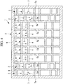
- Fig. 1 is a longitudinal sectional view illustrating a RF accelerating cavity according to the first embodiment of the present invention.
- This RF accelerating cavity 1 is included in the accelerator according to the present embodiment and uses, as an acceleration mode, a high-order mode such as a TM 0n mode (n > 1).
- the RF accelerating cavity 1 includes, for example, a plurality of accelerating cells 2 made of a dielectric, and a cylindrical housing 3 in which the plurality of accelerating cells 2 are disposed. Charged particles pass on the central axis of the RF accelerating cavity 1.
- the plurality of accelerating cells 2 are disposed in series in a beam axial direction from an end plate 7 on one side in the housing 3 to another end plate 7 on the other side.
- Each accelerating cell 2 includes a cylindrical barrel portion 4 and a circular disk portion 5.
- a circular ring portion 8 is provided outside of the cylindrical barrel portion 4 on a plane extending from the circular disk portion 5 provided inside of the cylindrical barrel portion 4. Accordingly, the cylindrical barrel portion 4 is connected with an integration of the circular disk portion 5 and the circular ring portion 8. The circular disk portion 5 is supported by an inner peripheral surface of the housing 3 through the circular ring portion 8.
- the cylindrical barrel portion 4, the circular disk portion 5, and the circular ring portion 8 is made of a dielectric with no metal coating or the like provided on a surface.
- the dielectric of the accelerating cell 2 in other words, the dielectric of the cylindrical barrel portion 4 and the circular disk portion 5 has a low dielectric loss and is ceramic such as alumina or sapphire.
- tan ⁇ dielectric tangent
- tan ⁇ dielectric tangent
- a development example of a dielectric having a low dielectric loss is ceramic (high-purity alumina) having a low dielectric loss of 7.5 ⁇ 10 -6 approximately at room temperature ( Applied Physics Letters, (USA), 2002, Vol. 81, No.26, pp. 5021-5023 ).
- the housing 3 includes a cylindrical barrel portion 6, and the circular plate end plates 7 provided at both side ends of the cylindrical barrel portion 6.
- the housing 3 is made of, for example, a highly conductive metallic material that is pure metal such as oxygen-free copper or stainless steel plated with silver or copper.
- the housing 3 may be made of a dielectric such as ceramic plated with silver or copper as appropriate. The use of such metal material or metal-plated dielectric provides conductivity at the surface of the housing 3.
- Each end plate 7 is a plate member provided with a circular opening 7a at the center.
- the cylindrical barrel portion 4 of each accelerating cell 2 has a central axis aligned with the central axis of the cylindrical barrel portion 6 of the housing 3, and has a diameter smaller than that of the cylindrical barrel portion 6 of the housing 3.
- the diameter of the cylindrical barrel portion 4 may be identical in all accelerating cells 2 or may be different among the accelerating cells 2.
- the diameter of the cylindrical barrel portion 4 may be set to be larger on an end part side than on a middle part side.
- the circular disk portion 5 is connected with an end part of the cylindrical barrel portion 4.
- the circular disk portion 5 of each accelerating cell 2 is a plate member provided with a circular opening 5a at the center.
- the opening 5a has a diameter smaller than that of the cylindrical barrel portion 4. Charged particles pass through the opening 5a.
- the cylindrical barrel portion 4 is installed orthogonal to the plane of the circular disk portion 5.
- the circular disk portion 5 is disposed at a position separated from each end plate 7 of the housing 3, and the cylindrical barrel portion 4 contacts with the end plate 7. Not every accelerating cell 2 includes the cylindrical barrel portion 4 and the circular disk portion 5, but only the cylindrical barrel portion 4 or the circular disk portion 5 may be included in some accelerating cells 2.
- the above-described configuration generates electric field in the direction of acceleration near the beam axis.
- the circular disk portion 5 including the opening 5a is installed inside of the cylindrical barrel portion 4 such that a plate surface of the circular disk portion 5 of each accelerating cell 2 is orthogonal to the beam axis. Accordingly, the acceleration electric field can be concentrated in the beam axial direction inside of the opening 5a of the circular disk portion 5, which leads to increase in shunt impedance.
- Electromagnetic field distribution in an acceleration mode excited inside the RF accelerating cavity 1 is adjusted by adjusting, for example, the inner and outer diameters of the cylindrical barrel portion 4 of each accelerating cell 2 disposed in the housing 3, intervals between the circular disk portions 5, the inner diameter of the opening 5a of each circular disk portion 5, and the inner diameter of the housing 3.
- the cylindrical barrel portion 4 allows accumulation of RF electrical power near the beam axis on which a charged particle beam passes. As a result, RF magnetic field generated in parallel to a metal surface of each end plate 7 of the housing 3 can be reduced, which leads to reduction of a conductor loss at the metal surface.
- the Q value is 60,000 approximately as illustrated in Fig. 2 , which is at least several times higher than that for a conventional normal-conducting accelerating cavity.
- the conventional normal-conducting accelerating cavity has a Q value of 10,000 approximately.
- Fig. 2 indicates that the Q value tends to become higher as the number of cells increases. This is because, as the number of cells increases, the RF accelerating cavity 1 is longer, and the ratio of an energy loss in the RF accelerating cavity 1 decreases.
- the structure of the RF accelerating cavity 1 was simulated by changing the inner and outer diameters of the cylindrical barrel portion 4 of the accelerating cell 2 and the inner diameter of the housing 3 so that electromagnetic field distribution in a ⁇ mode at a predetermined resonance frequency is excited in the RF accelerating cavity 1.
- the inner and outer diameters of the cylindrical barrel portion 4 and the inner diameter of the housing 3 were calculated from a result of the simulation. Then, the Q value was calculated by using the calculated structure.
- the ⁇ mode refers to a mode in which resonance electric fields having phases shifted from each other by 180° are alternately generated in vacuum parts each sandwiched between the circular disk portions 5 and including the beam axis.
- U represents the energy of electromagnetic wave accumulated in the RF accelerating cavity 1
- P_loss represents an energy loss of electromagnetic wave in the RF accelerating cavity 1 (per one period of electromagnetic wave)
- f represents the frequency of electromagnetic wave.
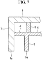
- the circular ring portion 8 is provided on the extending plane of the plate surface of the circular disk portion 5, but the present invention is not limited to this example. Specifically, the circular ring portions 8 do not need to be provided for the respective circular disk portions 5, but may be provided in a number smaller than the number of circular disk portions 5 or may be each provided at a position shifted from the extending plane of the circular disk portion 5 as illustrated in Fig. 7 , not on the extending plane of the circular disk portion 5. In other words, the circular ring portions 8 only need to be disposed between the inner peripheral surface of the housing 3 and the outer peripheral surface of the cylindrical barrel portion 4 to support the cylindrical barrel portions 4 and the circular disk portions 5.
- the Q value at least five times higher than that of an existing normal-conducting accelerating cavity at room temperature can be obtained, thereby achieving a RF accelerator having an electrical power efficiency higher than conventional cases.
- a cylindrical barrel portion 9 is provided around the beam axis in the accelerating cell 2 adjacent to each end plate 7 of the housing 3 among the accelerating cells 2.
- the cylindrical barrel portion 9 is provided to the accelerating cell 2 close to the end plate 7 on each side.
- the cylindrical barrel portion 9 has an inner diameter equal to that of the opening 5a of the circular disk portion 5, and has one end part connected with the corresponding end plate 7 of the housing 3 and the other end part connected with the circular disk portion 5 of the corresponding accelerating cell 2.
- the cylindrical barrel portion 9 is made of a dielectric same as those of the cylindrical barrel portion 4, the circular disk portion 5, and the circular ring portion 8 described in the first embodiment.
- the RF magnetic field generated in parallel to the metal surface is reduced at each end plate 7 of the housing 3 of the RF accelerating cavity 1.
- the additionally provided cylindrical barrel portion 9 leads to further reduction of the RF magnetic field generated in parallel to the metal surface.
- a calculation result of the Q value by the above-described calculation program based on the structure of the RF accelerating cavity 1 according to the second embodiment shows that the Q value is 100,000 or higher in a case of the five-cell structure.
- the structure of the RF accelerating cavity 1 according to the present embodiment can achieve the Q value about two times higher than that of the structure of the RF accelerating cavity 1 according to the first embodiment in which the cylindrical barrel portion 9 is not installed. Accordingly, a RF accelerator having an electrical power efficiency higher than conventional cases can be achieved.
- the RF accelerating cavity 1 according to a third embodiment of the present invention with reference to Fig. 4 .
- a plurality of cylindrical barrel portions 4 having diameters different from each other are concentrically provided in each accelerating cell 2.
- the RF accelerating cavity 1 can use a high-order mode as an acceleration mode.
- the Q value can be further increased.
- Fig. 4 illustrates an example in which two cylindrical barrel portions 4 are provided.
- the cylindrical barrel portions 4 When two or more cylindrical barrel portions 4 are provided, the cylindrical barrel portions 4 have central axes aligned on an identical axis and are concentrically installed in each accelerating cell 2.
- the number of the cylindrical barrel portions 4 is n-1, where n represents the order of the acceleration mode of the RF accelerating cavity. Specifically, one cylindrical barrel portion 4 is provided when the acceleration mode order is two, and two cylindrical barrel portions 4 are provided when the acceleration mode order is three.
- the cylindrical barrel portion 9 is installed around the beam axis in the accelerating cell 2 close to each end plate 7 of the housing 3 among the accelerating cells 2.
- the cylindrical barrel portions 9 are provided to the n-1 accelerating cells 2 on each end side, where n represents the order of the acceleration mode of the RF accelerating cavity.
- n represents the order of the acceleration mode of the RF accelerating cavity.
- the cylindrical barrel portions 9 are installed in the two accelerating cells 2 closest to each end plate 7 of the housing 3.
- the cylindrical barrel portions 9 are provided to the accelerating cells 2 close to the end plates 7 of the housing 3.
- no cylindrical barrel portion 9 may be provided in the RF accelerating cavity 1 that employs any high-order mode as the acceleration mode, similarly to the first embodiment.
- Fig. 5 illustrates a calculation result of the unloaded Q value when tan ⁇ as an index illustrating the dielectric loss of the dielectric used for the accelerating cells 2 is changed in each case in which the number of provided cylindrical barrel portions 4 is one, two, or three.
- the surface resistance of copper is a value at room temperature.
- Fig. 5 indicates that the unloaded Q value increases with increase in the number of dielectric cylindrical barrel portions 4 in each accelerating cell 2.
- increase in the number of cylindrical barrel portions 4 can reduce electric field generated at the conductive surface of the housing 3 at a high-order mode. This leads to reduction of an energy loss, thereby increasing the Q value. Accordingly, the acceleration electric field can be concentrated in the beam axial direction.
- Fig. 6 illustrates a calculation result of the unloaded Q value when the temperature of environment in which the RF accelerating cavity 1 is used is changed in each case in which the number of provided cylindrical barrel portions 4 is one, two, or three.
- the calculation obtains the unloaded Q value for a case in which high-purity copper having a residual resistance ratio (RRR) of 2000 or higher is used as the metal of the housing 3, and the entire RF accelerating cavity 1 is cooled to liquid nitrogen temperature.
- RRR residual resistance ratio
- the calculation result indicates that the Q value and shunt impedance of the RF accelerating cavity 1 can be improved by cooling the entire RF accelerating cavity 1. Specifically, when the entire RF accelerating cavity 1 is cooled, the temperature of the housing 3 decreases and electric resistance decreases accordingly, which leads to reduction of an energy loss in the housing 3.
- Fig. 6 indicates that the unloaded Q value increases as the temperature decreases when the number of provided cylindrical barrel portions 4 is any of one, two, and three, and that the increase of the Q value is larger as the number of layers of cylindrical barrel portions 4 increases.
- the cooling to liquid nitrogen temperature can lead to the Q value about 100 times higher than a case with room temperature, thereby achieving high shunt impedance.
- no metal coating is provided to the dielectric in the cylindrical barrel portion 4, the circular disk portion 5, and the circular ring portion 8 of each accelerating cell 2 in the RF accelerating cavity 1.
- the cylindrical barrel portion 4, the circular disk portion 5, and the circular ring portion 8 may be provided with metal coating.
- Metal coating is, for example, coating with TiN, and provided in a thickness of several nanometers approximately.
- the TiN coating provided on the surface of the dielectric leads to reduction of the secondary electron emission coefficient of each accelerating cell 2 when an accelerator is operational.
- the secondary electron emission coefficient which is 4.8 for HA95 (purity at 95%) and 6.5 for HA997 (purity at 99.7%) in which the dielectric is alumina
- the secondary electron emission coefficient equal to two or lower is substantially same as that of an existing normal-conducting accelerating cavity.
- the decrease of the secondary electron emission coefficient reduces the probability of electrical discharging due to the multipactor effect at a ceramic surface when high electric field is applied to the RF accelerating cavity 1, thereby achieving more stable operation.
Landscapes
- Physics & Mathematics (AREA)
- Engineering & Computer Science (AREA)
- Plasma & Fusion (AREA)
- Spectroscopy & Molecular Physics (AREA)
- Particle Accelerators (AREA)
Abstract
Description
- The present invention relates to an accelerating cavity and an accelerator.
- In a radio-frequency (RF) accelerating cavity used for a charged particle accelerator, RF electrical power is accumulated in a metal housing, and charged particles such as electrons and ions are artificially accelerated to high speed by using RF electric field generated in the housing. Accelerators using a RF accelerating cavity are widely used in, for example, the academic fields of high-energy physics experiments and synchrotron radiation facilities and the industrial fields of radiation therapy and diagnostic devices and sterilization devices.
- Typically, a RF accelerating cavity is roughly classified into a normal-conducting accelerating cavity that is made of high-purity copper and operates at room temperature, and a superconducting accelerating cavity that is made of superconductive material (for example, niobium) and operates at extremely low temperature.
- PTL 1 discloses an invention related to an accelerating structure produced by alternately joining a ring-shaped acceleration member made of non-magnetic refractory metal and a ring-shaped electrical insulation member made of ceramic.
PTL 2 discloses an invention related to an accelerating cavity produced by alternately connecting a basic cavity and a disk in an acceleration direction, in which the basic cavity and the disk are manufactured by forming two layers of an active silver brazing filler metal layer and a copper electroforming layer on the surface of each of a ceramic cavity and a ceramic circular disk. -
- [PTL 1]
Japanese Unexamined Patent Application, Publication No.S63-28447 - [PTL 2]
Japanese Unexamined Patent Application, Publication No.2003-303700 - To achieve energy increase and downsizing of an accelerator in which a large number of acceleration cavities are coupled, RF accelerating cavities each having a high Q value in a low-temperature region lower than room temperature by several tens Kelvin are required when building and operation costs are taken into consideration. The Q value indicates an accumulation efficiency of RF electrical power of an accelerating cavity, and the value is largely determined by the electric conductivity of the material of the accelerating cavity. Thus, the Q value of any existing accelerating cavity made of metal is limited by the electric conductivity, which is a physical property intrinsic to metal, and thus cannot be much further increased.
- For example, the Q value of an existing normal-conducting accelerating cavity can be increased by cooling accelerating cavities to low temperature. Typically, the electric conductivity of a normal conductor is significantly increased by cooling, and for example, when cooled to 20 K, the normal conductor obtains an
electric conductivity 104 times higher than at room temperature. However, RF electrical power is additionally lost due to a high-frequency loss mechanism called anomalous skin effect, which is different from that at room temperature. Thus, although high electric conductivity can be obtained by cooling acceleration cavities, the Q value is only increased to about 5.5 times higher than that at room temperature, for example, when the acceleration cavities are cooled to 20 K approximately, which is not significant increase. - A dielectric-loaded RF acceleration structure includes a cylindrical barrel member that is made of ceramic and an outer periphery part of which is coated with metal. The Q value of an existing dielectric-loaded RF acceleration structure exploiting a TM01 mode is almost same as that of a normal-conducting accelerating cavity. Moreover, in a dielectric-loaded RF acceleration structure, most of RF electrical power accumulated inside a cavity is accumulated inside dielectric, and only an extremely small part of the electrical power is available for charged particle acceleration. Thus, the dielectric-loaded RF acceleration structure has extremely small shunt impedance as compared to that of any existing accelerating cavity.
- The present invention is intended to solve the above-described problems by providing an accelerating cavity and an accelerator that are capable of obtaining Q values and electrical power efficiencies higher than those of a conventional normal-conducting accelerating cavity.
- An accelerating cavity according to a first aspect of the present invention includes: a housing having an inner peripheral surface in a tubular shape and conductivity on a surface; and a plurality of cells provided inside the housing and each made of a dielectric including, at a central part, an opening through which a charged particle passes. The housing includes a barrel portion having a tubular shape and end plates installed at both ends of the barrel portion. The plurality of cells are disposed in a range extending from the end plate on one end side of the housing to the end plate on the other end side. Each cell includes: a cylindrical barrel portion having a diameter smaller than an inner diameter of the barrel portion of the housing; and a plate portion provided inside of the cylindrical barrel portion to be fixed to the cylindrical barrel portion, and disposed such that a plate surface is orthogonal to a passing axis of the charged particle, and provided with the opening.
- With this configuration, the accelerating cavity includes the housing having the conductive surface, and the plurality of cells each made of a dielectric, in particular, a dielectric with a relatively low dielectric loss, and a charged particle is accelerated while passing through the opening provided at the central part of each cell. Electric field is generated in the direction of acceleration near the passing axis of a charged particle. The plate portion including the opening is installed inside of the cylindrical barrel portion of each cell such that the plate surface of the plate portion of the cell is orthogonal to the passing axis of a charged particle. Accordingly, the acceleration electric field can be concentrated in the direction of the passing axis of a charged particle inside of the opening of the plate portion, which leads to increase in shunt impedance. Since the cylindrical barrel portion has a diameter smaller than the inner diameter of the barrel portion of the housing, RF electrical power can be accumulated near the passing axis on which a charged particle beam passes. In addition, RF magnetic field generated in parallel to a metal surface of each end plate of the housing can be reduced, which leads to reduction of a conductor loss at the metal surface.
- In the first aspect, tanδ as an index indicating a dielectric loss is equal to or smaller than 1×10⁻³, more preferably 1×10⁻⁵, for the dielectric.
- In the first aspect, a cell adjacent to the end plate of the housing among the plurality of cells may further include a second cylindrical barrel portion provided around the passing axis, and the second cylindrical barrel portion may be connected with the end plate and the plate portion of the cell adjacent to the end plate.
- With this configuration, the additionally provided second cylindrical barrel portion leads to further reduction of the RF magnetic field generated in parallel to the metal surface.
- In the first aspect, a plurality of the cylindrical barrel portions having diameters different from each other may be concentrically disposed in each cell of the plurality of cells.
- With this configuration, a high-order mode can be used as an acceleration mode, and as a result, the Q value can be further increased.
- In the first aspect, the number of the plurality of cylindrical barrel portions in each cell is n-1, where n represents the order of an acceleration mode.
- In the first aspect, each cell may have a surface coated with titanium nitride (TiN).
- This configuration leads to reduction of the secondary electron emission coefficient of the cell in operation.
- An accelerator according to a second aspect of the present invention includes the above-described accelerating cavity.
- The present invention can achieve a Q value higher than that of any conventional normal-conducting accelerating cavity, and thus achieve increased electrical power efficiency.
-
- [
Fig. 1 ]
Fig. 1 is a longitudinal sectional view illustrating a RF accelerating cavity according to a first embodiment of the present invention. - [
Fig. 2 ]
Fig. 2 is a graph illustrating the relation between the number of accelerating cells and the unloaded Q value of the RF accelerating cavity. - [
Fig. 3 ]
Fig. 3 is a longitudinal sectional view illustrating the RF accelerating cavity according to a second embodiment of the present invention. - [
Fig. 4 ]
Fig. 4 is a longitudinal sectional view illustrating the RF accelerating cavity according to a third embodiment of the present invention. - [
Fig. 5 ]
Fig. 5 is a graph illustrating the relation between tanδ as an index indicating the dielectric loss of a dielectric and the unloaded Q value of the RF accelerating cavity. - [
Fig. 6 ]
Fig. 6 is a graph illustrating the relation between tanδ as an index indicating the dielectric loss of a dielectric and the temperature. - [
Fig. 7 ]
Fig. 7 is a partially longitudinal sectional view illustrating the RF accelerating cavity according to a modification of the first embodiment of the present invention. - Embodiments of the present invention will be described below with reference to the accompanying drawings.
- The following describes an accelerator according to a first embodiment of the present invention with reference to
Fig. 1. Fig. 1 is a longitudinal sectional view illustrating a RF accelerating cavity according to the first embodiment of the present invention. - This RF accelerating cavity 1 is included in the accelerator according to the present embodiment and uses, as an acceleration mode, a high-order mode such as a TM0n mode (n > 1).
- The RF accelerating cavity 1 includes, for example, a plurality of accelerating
cells 2 made of a dielectric, and acylindrical housing 3 in which the plurality of acceleratingcells 2 are disposed. Charged particles pass on the central axis of the RF accelerating cavity 1. - The plurality of accelerating
cells 2 are disposed in series in a beam axial direction from anend plate 7 on one side in thehousing 3 to anotherend plate 7 on the other side. Each acceleratingcell 2 includes acylindrical barrel portion 4 and acircular disk portion 5. - To achieve convenience in manufacturing of the accelerating
cell 2 and a reliable support structure, acircular ring portion 8 is provided outside of thecylindrical barrel portion 4 on a plane extending from thecircular disk portion 5 provided inside of thecylindrical barrel portion 4. Accordingly, thecylindrical barrel portion 4 is connected with an integration of thecircular disk portion 5 and thecircular ring portion 8. Thecircular disk portion 5 is supported by an inner peripheral surface of thehousing 3 through thecircular ring portion 8. - The
cylindrical barrel portion 4, thecircular disk portion 5, and thecircular ring portion 8 is made of a dielectric with no metal coating or the like provided on a surface. The dielectric of the acceleratingcell 2, in other words, the dielectric of thecylindrical barrel portion 4 and thecircular disk portion 5 has a low dielectric loss and is ceramic such as alumina or sapphire. In the present embodiment, tanδ (dielectric tangent), which is an index indicating the dielectric loss of the dielectric of thecylindrical barrel portion 4, thecircular disk portion 5, and thecircular ring portion 8, is 1×10⁻³ or smaller, for example. - A development example of a dielectric having a low dielectric loss is ceramic (high-purity alumina) having a low dielectric loss of 7.5×10⁻⁶ approximately at room temperature (Applied Physics Letters, (USA), 2002, Vol. 81, No.26, pp. 5021-5023). In addition, a preceding research related to the quality of a low-loss dielectric provides an experiment result that, for example, tanδ of sapphire is proportional to temperature T [K] to the power of five, and tanδ = 10-5 at room temperature decreases to tanδ = 10-7 at 80 K (Physics Letters A, (Holland), 1987, Vol. 120, No.6, pp. 300-305).
- The
housing 3 includes acylindrical barrel portion 6, and the circularplate end plates 7 provided at both side ends of thecylindrical barrel portion 6. Thehousing 3 is made of, for example, a highly conductive metallic material that is pure metal such as oxygen-free copper or stainless steel plated with silver or copper. Alternatively, thehousing 3 may be made of a dielectric such as ceramic plated with silver or copper as appropriate. The use of such metal material or metal-plated dielectric provides conductivity at the surface of thehousing 3. Eachend plate 7 is a plate member provided with acircular opening 7a at the center. - The
cylindrical barrel portion 4 of each acceleratingcell 2 has a central axis aligned with the central axis of thecylindrical barrel portion 6 of thehousing 3, and has a diameter smaller than that of thecylindrical barrel portion 6 of thehousing 3. The diameter of thecylindrical barrel portion 4 may be identical in all acceleratingcells 2 or may be different among the acceleratingcells 2. For example, the diameter of thecylindrical barrel portion 4 may be set to be larger on an end part side than on a middle part side. Thecircular disk portion 5 is connected with an end part of thecylindrical barrel portion 4. - The
circular disk portion 5 of each acceleratingcell 2 is a plate member provided with acircular opening 5a at the center. Theopening 5a has a diameter smaller than that of thecylindrical barrel portion 4. Charged particles pass through theopening 5a. Thecylindrical barrel portion 4 is installed orthogonal to the plane of thecircular disk portion 5. Thecircular disk portion 5 is disposed at a position separated from eachend plate 7 of thehousing 3, and thecylindrical barrel portion 4 contacts with theend plate 7. Not every acceleratingcell 2 includes thecylindrical barrel portion 4 and thecircular disk portion 5, but only thecylindrical barrel portion 4 or thecircular disk portion 5 may be included in some acceleratingcells 2. - The above-described configuration generates electric field in the direction of acceleration near the beam axis. The
circular disk portion 5 including theopening 5a is installed inside of thecylindrical barrel portion 4 such that a plate surface of thecircular disk portion 5 of each acceleratingcell 2 is orthogonal to the beam axis. Accordingly, the acceleration electric field can be concentrated in the beam axial direction inside of theopening 5a of thecircular disk portion 5, which leads to increase in shunt impedance. - Electromagnetic field distribution in an acceleration mode excited inside the RF accelerating cavity 1 is adjusted by adjusting, for example, the inner and outer diameters of the
cylindrical barrel portion 4 of each acceleratingcell 2 disposed in thehousing 3, intervals between thecircular disk portions 5, the inner diameter of theopening 5a of eachcircular disk portion 5, and the inner diameter of thehousing 3. Thecylindrical barrel portion 4 allows accumulation of RF electrical power near the beam axis on which a charged particle beam passes. As a result, RF magnetic field generated in parallel to a metal surface of eachend plate 7 of thehousing 3 can be reduced, which leads to reduction of a conductor loss at the metal surface. - For example, in a case of a five-cell structure including five accelerating
cells 2, the Q value is 60,000 approximately as illustrated inFig. 2 , which is at least several times higher than that for a conventional normal-conducting accelerating cavity. When made of copper, the conventional normal-conducting accelerating cavity has a Q value of 10,000 approximately.Fig. 2 indicates that the Q value tends to become higher as the number of cells increases. This is because, as the number of cells increases, the RF accelerating cavity 1 is longer, and the ratio of an energy loss in the RF accelerating cavity 1 decreases. - Calculation that derived the result of the Q value illustrated in
Fig. 2 was performed by a calculation program (Poisson Superfish: Los Alamos national laboratory (http://laacg.lanl.gov/laacg/services/download_sf.phtml)). - The calculation was performed under conditions as follows: the physical properties of high-purity alumina (Applied Physics Letters, (USA), 2002, Vol. 81, No.26, pp. 5021-5023) described above were used for the dielectric of the
cylindrical barrel portion 4 and thecircular disk portion 5 of each acceleratingcell 2, and the physical properties of oxygen-free copper were used for the metal of thehousing 3. The structure of the RF accelerating cavity 1 was simulated by changing the inner and outer diameters of thecylindrical barrel portion 4 of the acceleratingcell 2 and the inner diameter of thehousing 3 so that electromagnetic field distribution in a π mode at a predetermined resonance frequency is excited in the RF accelerating cavity 1. The inner and outer diameters of thecylindrical barrel portion 4 and the inner diameter of thehousing 3 were calculated from a result of the simulation. Then, the Q value was calculated by using the calculated structure. The π mode refers to a mode in which resonance electric fields having phases shifted from each other by 180° are alternately generated in vacuum parts each sandwiched between thecircular disk portions 5 and including the beam axis. - The Q value is given by an expression below.

- In the expression, U represents the energy of electromagnetic wave accumulated in the RF accelerating cavity 1, P_loss represents an energy loss of electromagnetic wave in the RF accelerating cavity 1 (per one period of electromagnetic wave), and f represents the frequency of electromagnetic wave.
- In the above-described example, the
circular ring portion 8 is provided on the extending plane of the plate surface of thecircular disk portion 5, but the present invention is not limited to this example. Specifically, thecircular ring portions 8 do not need to be provided for the respectivecircular disk portions 5, but may be provided in a number smaller than the number ofcircular disk portions 5 or may be each provided at a position shifted from the extending plane of thecircular disk portion 5 as illustrated inFig. 7 , not on the extending plane of thecircular disk portion 5. In other words, thecircular ring portions 8 only need to be disposed between the inner peripheral surface of thehousing 3 and the outer peripheral surface of thecylindrical barrel portion 4 to support thecylindrical barrel portions 4 and thecircular disk portions 5. - According to the present embodiment described above, the Q value at least five times higher than that of an existing normal-conducting accelerating cavity at room temperature can be obtained, thereby achieving a RF accelerator having an electrical power efficiency higher than conventional cases.
- The following describes the RF accelerating cavity 1 according to a second embodiment of the present invention with reference to
Fig. 3 . In the RF accelerating cavity 1 according to the present embodiment, acylindrical barrel portion 9 is provided around the beam axis in the acceleratingcell 2 adjacent to eachend plate 7 of thehousing 3 among the acceleratingcells 2. Thecylindrical barrel portion 9 is provided to the acceleratingcell 2 close to theend plate 7 on each side. Thecylindrical barrel portion 9 has an inner diameter equal to that of theopening 5a of thecircular disk portion 5, and has one end part connected with thecorresponding end plate 7 of thehousing 3 and the other end part connected with thecircular disk portion 5 of the corresponding acceleratingcell 2. - The
cylindrical barrel portion 9 is made of a dielectric same as those of thecylindrical barrel portion 4, thecircular disk portion 5, and thecircular ring portion 8 described in the first embodiment. - In the first embodiment, the RF magnetic field generated in parallel to the metal surface is reduced at each
end plate 7 of thehousing 3 of the RF accelerating cavity 1. In the present embodiment, the additionally providedcylindrical barrel portion 9 leads to further reduction of the RF magnetic field generated in parallel to the metal surface. - A calculation result of the Q value by the above-described calculation program based on the structure of the RF accelerating cavity 1 according to the second embodiment shows that the Q value is 100,000 or higher in a case of the five-cell structure. Thus, the structure of the RF accelerating cavity 1 according to the present embodiment can achieve the Q value about two times higher than that of the structure of the RF accelerating cavity 1 according to the first embodiment in which the
cylindrical barrel portion 9 is not installed. Accordingly, a RF accelerator having an electrical power efficiency higher than conventional cases can be achieved. - The following describes the RF accelerating cavity 1 according to a third embodiment of the present invention with reference to
Fig. 4 . In the RF accelerating cavity 1 according to the present embodiment, a plurality ofcylindrical barrel portions 4 having diameters different from each other are concentrically provided in each acceleratingcell 2. With this configuration, the RF accelerating cavity 1 can use a high-order mode as an acceleration mode. As a result, the Q value can be further increased. - In the first embodiment, only one
cylindrical barrel portion 4 is provided in each acceleratingcell 2, but the present invention is not limited to this example. Two or morecylindrical barrel portions 4 may be provided.Fig. 4 illustrates an example in which twocylindrical barrel portions 4 are provided. - When two or more
cylindrical barrel portions 4 are provided, thecylindrical barrel portions 4 have central axes aligned on an identical axis and are concentrically installed in each acceleratingcell 2. The number of thecylindrical barrel portions 4 is n-1, where n represents the order of the acceleration mode of the RF accelerating cavity. Specifically, onecylindrical barrel portion 4 is provided when the acceleration mode order is two, and twocylindrical barrel portions 4 are provided when the acceleration mode order is three. - In the example illustrated in
Fig. 4 , similarly to the second embodiment, thecylindrical barrel portion 9 is installed around the beam axis in the acceleratingcell 2 close to eachend plate 7 of thehousing 3 among the acceleratingcells 2. Thecylindrical barrel portions 9 are provided to the n-1 acceleratingcells 2 on each end side, where n represents the order of the acceleration mode of the RF accelerating cavity. For example, when the twocylindrical barrel portions 4 are provided and the order of the acceleration mode is three, thecylindrical barrel portions 9 are installed in the two acceleratingcells 2 closest to eachend plate 7 of thehousing 3. - In the present embodiment, similarly to the second embodiment, the
cylindrical barrel portions 9 are provided to the acceleratingcells 2 close to theend plates 7 of thehousing 3. However, nocylindrical barrel portion 9 may be provided in the RF accelerating cavity 1 that employs any high-order mode as the acceleration mode, similarly to the first embodiment. -
Fig. 5 illustrates a calculation result of the unloaded Q value when tanδ as an index illustrating the dielectric loss of the dielectric used for the acceleratingcells 2 is changed in each case in which the number of providedcylindrical barrel portions 4 is one, two, or three. In this calculation, the surface resistance of copper is a value at room temperature. - The result illustrated in
Fig. 5 indicates that the unloaded Q value increases with increase in the number of dielectriccylindrical barrel portions 4 in each acceleratingcell 2. - Specifically, increase in the number of
cylindrical barrel portions 4 can reduce electric field generated at the conductive surface of thehousing 3 at a high-order mode. This leads to reduction of an energy loss, thereby increasing the Q value. Accordingly, the acceleration electric field can be concentrated in the beam axial direction. -
Fig. 6 illustrates a calculation result of the unloaded Q value when the temperature of environment in which the RF accelerating cavity 1 is used is changed in each case in which the number of providedcylindrical barrel portions 4 is one, two, or three. The calculation obtains the unloaded Q value for a case in which high-purity copper having a residual resistance ratio (RRR) of 2000 or higher is used as the metal of thehousing 3, and the entire RF accelerating cavity 1 is cooled to liquid nitrogen temperature. - The calculation result indicates that the Q value and shunt impedance of the RF accelerating cavity 1 can be improved by cooling the entire RF accelerating cavity 1. Specifically, when the entire RF accelerating cavity 1 is cooled, the temperature of the
housing 3 decreases and electric resistance decreases accordingly, which leads to reduction of an energy loss in thehousing 3.Fig. 6 indicates that the unloaded Q value increases as the temperature decreases when the number of providedcylindrical barrel portions 4 is any of one, two, and three, and that the increase of the Q value is larger as the number of layers ofcylindrical barrel portions 4 increases. - In a three-layer structure in which the number of provided
cylindrical barrel portions 4 is three, the cooling to liquid nitrogen temperature can lead to the Q value about 100 times higher than a case with room temperature, thereby achieving high shunt impedance. - In the above-described first to third embodiments, no metal coating is provided to the dielectric in the
cylindrical barrel portion 4, thecircular disk portion 5, and thecircular ring portion 8 of each acceleratingcell 2 in the RF accelerating cavity 1. However, thecylindrical barrel portion 4, thecircular disk portion 5, and thecircular ring portion 8 may be provided with metal coating. - Metal coating is, for example, coating with TiN, and provided in a thickness of several nanometers approximately. The TiN coating provided on the surface of the dielectric leads to reduction of the secondary electron emission coefficient of each accelerating
cell 2 when an accelerator is operational. In a known case (Yuko Kijima et al., "the secondary electron emission coefficient of the material for the superconducting cavity input coupler", vacuum, the vacuum society of Japan, 2002, Vol. 45, 7, pp.599-603) in which the dielectric is alumina, the secondary electron emission coefficient, which is 4.8 for HA95 (purity at 95%) and 6.5 for HA997 (purity at 99.7%), can be decreased to two or lower by the TiN coating. The secondary electron emission coefficient equal to two or lower is substantially same as that of an existing normal-conducting accelerating cavity. - The decrease of the secondary electron emission coefficient reduces the probability of electrical discharging due to the multipactor effect at a ceramic surface when high electric field is applied to the RF accelerating cavity 1, thereby achieving more stable operation.
-
- 1
- RF accelerating cavity
- 2
- accelerating cell
- 3
- housing
- 4
- cylindrical barrel portion
- 5
- circular disk portion
- 6
- cylindrical barrel portion
- 7
- end plate
- 8
- circular ring portion
- 9
- cylindrical barrel portion
Claims (8)
- An accelerating cavity comprising:a housing having an inner peripheral surface in a tubular shape and conductivity on a surface; anda plurality of cells provided inside the housing and each made of a dielectric including, at a central part, an opening through which a charged particle passes, whereinthe housing includes a barrel portion having a tubular shape and end plates installed at both ends of the barrel portion,the plurality of cells are disposed in a range extending from the end plate on one end side of the housing to the end plate on the other end side, andeach cell includes:a cylindrical barrel portion having a diameter smaller than an inner diameter of the barrel portion of the housing; anda plate portion provided inside of the cylindrical barrel portion to be fixed to the cylindrical barrel portion, and disposed such that a plate surface is orthogonal to a passing axis of the charged particle, and provided with the opening.
- The accelerating cavity according to claim 1, wherein tanδ as an index indicating a dielectric loss is equal to or smaller than 1×10⁻³ for the dielectric.
- The accelerating cavity according to claim 1, wherein tanδ as an index indicating a dielectric loss is equal to or smaller than 1×10⁻⁵ for the dielectric.
- The accelerating cavity according to any one of claims 1 to 3, wherein
a cell adjacent to the end plate of the housing among the plurality of cells further includes a second cylindrical barrel portion provided around the passing axis, and
the second cylindrical barrel portion is connected with the end plate and the plate portion of the cell adjacent to the end plate. - The accelerating cavity according to any one of claims 1 to 4, wherein a plurality of the cylindrical barrel portions having diameters different from each other are concentrically disposed in each cell of the plurality of cells.
- The accelerating cavity according to claim 5, wherein the number of the plurality of cylindrical barrel portions in each cell is n-1, where n represents the order of an acceleration mode.
- The accelerating cavity according to any one of claims 1 to 6, wherein each cell has a surface coated with TiN.
- An accelerator comprising the accelerating cavity according to any one of claims 1 to 7.
Applications Claiming Priority (2)
| Application Number | Priority Date | Filing Date | Title |
|---|---|---|---|
| JP2015254039A JP6650146B2 (en) | 2015-12-25 | 2015-12-25 | Acceleration cavity and accelerator |
| PCT/JP2016/087683 WO2017110700A1 (en) | 2015-12-25 | 2016-12-16 | Acceleration cavity and accelerator |
Publications (3)
| Publication Number | Publication Date |
|---|---|
| EP3397032A1 true EP3397032A1 (en) | 2018-10-31 |
| EP3397032A4 EP3397032A4 (en) | 2019-08-28 |
| EP3397032B1 EP3397032B1 (en) | 2022-06-08 |
Family
ID=59090299
Family Applications (1)
| Application Number | Title | Priority Date | Filing Date |
|---|---|---|---|
| EP16878589.7A Active EP3397032B1 (en) | 2015-12-25 | 2016-12-16 | Acceleration cavity and accelerator |
Country Status (6)
| Country | Link |
|---|---|
| US (1) | US10440809B2 (en) |
| EP (1) | EP3397032B1 (en) |
| JP (1) | JP6650146B2 (en) |
| KR (1) | KR102044111B1 (en) |
| CN (1) | CN108432350B (en) |
| WO (1) | WO2017110700A1 (en) |
Families Citing this family (3)
| Publication number | Priority date | Publication date | Assignee | Title |
|---|---|---|---|---|
| US10897069B2 (en) | 2018-10-02 | 2021-01-19 | International Business Machines Corporation | Reduced kapitza resistance microwave filter for cryogenic environments |
| JP7253401B2 (en) * | 2019-02-06 | 2023-04-06 | 三菱重工機械システム株式会社 | Radiation generator and radiation generation method |
| JP7209293B2 (en) * | 2019-05-17 | 2023-01-20 | 三菱重工機械システム株式会社 | accelerating cavity |
Family Cites Families (18)
| Publication number | Priority date | Publication date | Assignee | Title |
|---|---|---|---|---|
| US2916710A (en) | 1951-07-16 | 1959-12-08 | Walkinshaw William | Loaded wave-guides for linear accelerators |
| JPS6328447A (en) | 1986-07-21 | 1988-02-06 | Toshiba Corp | Accelerating tube |
| JPH0256900A (en) * | 1988-08-23 | 1990-02-26 | Mitsubishi Electric Corp | Accelerating tube |
| US5532210A (en) * | 1994-06-08 | 1996-07-02 | E. I. Du Pont De Nemours And Company | High temperature superconductor dielectric slow wave structures for accelerators and traveling wave tubes |
| US5546743A (en) * | 1994-12-08 | 1996-08-20 | Conner; Paul H. | Electron propulsion unit |
| JP2742770B2 (en) * | 1995-04-12 | 1998-04-22 | 電気興業株式会社 | High frequency particle accelerator |
| JP3243683B2 (en) * | 1995-06-23 | 2002-01-07 | 株式会社日立製作所 | Accelerator tube and accelerator for charged particle acceleration, charged particle gun and standing wave accelerating cavity |
| US5811943A (en) * | 1996-09-23 | 1998-09-22 | Schonberg Research Corporation | Hollow-beam microwave linear accelerator |
| JPH1126194A (en) * | 1997-07-01 | 1999-01-29 | Ishikawajima Harima Heavy Ind Co Ltd | Accelerator tube and method for preventing reflection of high-frequency electromagnetic waves |
| JP3868322B2 (en) | 2002-04-10 | 2007-01-17 | 三菱重工業株式会社 | Ceramic acceleration cavity, accelerator equipped with the acceleration cavity, and method of manufacturing a ceramic acceleration cavity |
| ITMI20022608A1 (en) * | 2002-12-09 | 2004-06-10 | Fond Di Adroterapia Oncologic A Tera | LINAC WITH DRAWING TUBES FOR THE ACCELERATION OF A BAND OF IONS. |
| CN1220411C (en) * | 2003-07-26 | 2005-09-21 | 中国工程物理研究院应用电子学研究所 | Standing wave electronic straight line accelerator |
| JP2007087846A (en) * | 2005-09-26 | 2007-04-05 | Kyocera Corp | Accelerating tube |
| JP5449019B2 (en) * | 2010-05-12 | 2014-03-19 | 三菱重工業株式会社 | Superconducting acceleration cavity and method of manufacturing superconducting acceleration cavity |
| CN201758483U (en) * | 2010-08-26 | 2011-03-09 | 合肥中科大爱克科技有限公司 | Coaxial absorbing load device of travelling wave electronic linear accelerator |
| DE102010044113A1 (en) * | 2010-11-18 | 2012-05-24 | Siemens Aktiengesellschaft | RF cavity and particle accelerator with RF cavity |
| US9671520B2 (en) * | 2014-02-07 | 2017-06-06 | Euclid Techlabs, Llc | Dielectric loaded particle accelerator |
| CN104837293A (en) * | 2015-04-10 | 2015-08-12 | 中广核中科海维科技发展有限公司 | An energy adjustment device for an accelerating tube capable of converting and outputting keV and MeV rays |
-
2015
- 2015-12-25 JP JP2015254039A patent/JP6650146B2/en active Active
-
2016
- 2016-12-16 KR KR1020187017907A patent/KR102044111B1/en active Active
- 2016-12-16 CN CN201680074449.XA patent/CN108432350B/en active Active
- 2016-12-16 EP EP16878589.7A patent/EP3397032B1/en active Active
- 2016-12-16 US US16/065,776 patent/US10440809B2/en active Active
- 2016-12-16 WO PCT/JP2016/087683 patent/WO2017110700A1/en not_active Ceased
Also Published As
| Publication number | Publication date |
|---|---|
| EP3397032B1 (en) | 2022-06-08 |
| EP3397032A4 (en) | 2019-08-28 |
| JP2017117730A (en) | 2017-06-29 |
| JP6650146B2 (en) | 2020-02-19 |
| CN108432350B (en) | 2020-11-27 |
| US20190014653A1 (en) | 2019-01-10 |
| US10440809B2 (en) | 2019-10-08 |
| KR20180088418A (en) | 2018-08-03 |
| KR102044111B1 (en) | 2019-11-12 |
| CN108432350A (en) | 2018-08-21 |
| WO2017110700A1 (en) | 2017-06-29 |
Similar Documents
| Publication | Publication Date | Title |
|---|---|---|
| CN103766006B (en) | Compact cold superconduction isochronous cyclotron | |
| JP5481070B2 (en) | Magnetic field generation method for particle acceleration, magnet structure, and manufacturing method thereof | |
| US10440809B2 (en) | Accelerating cavity and accelerator | |
| WO2021055037A2 (en) | Techniques for direct deposition of superconductor material and related systems and methods | |
| Satoh et al. | Fabrication and cold test of dielectric assist accelerating structure | |
| US11008650B2 (en) | Compact system for coupling RF power directly into RF linacs | |
| Xiao et al. | Design and high-power test of 800-kW UHF klystron for CEPC | |
| JP7644145B2 (en) | Techniques for distributing forces in high field magnets and related systems and methods - Patents.com | |
| Crawford et al. | High gradients in linear collider superconducting accelerator cavities by high pulsed power to suppress field emission | |
| Suetsugu et al. | Design studies on a vacuum bellows assembly with radio frequency shield for the KEK B factory | |
| Hwang et al. | Development trends for insertion devices of future synchrotron light sources | |
| TWI458397B (en) | Magnet structure for particle acceleration | |
| Mitsunobu et al. | High power input coupler for KEKB SC cavity | |
| CN105869973B (en) | Axially export the compact magnetron of circular polarisation TE11 coaxial waveguide patterns | |
| US10448496B2 (en) | Superconducting cavity coupler | |
| US11227706B2 (en) | Superconducting wire and coil unit | |
| Liepe | Superconducting RF for the Future: Is Nb 3 Sn Ready for Next-generation Accelerators? | |
| WO1998033228A2 (en) | High-gradient insulator cavity mode filter | |
| Labrie et al. | The coaxial coupled linac structure | |
| Xu et al. | Measurement of internal dark current in a 17 GHz accelerator structure with an elliptical sidewall | |
| Bauer et al. | Production of Nb/Cu sputtered superconducting cavities for LHC | |
| McEuen et al. | High-power operation of accelerator structures at liquid nitrogen temperature | |
| Park et al. | Compact Self-Matching Microwave Plasma Source with a Wide Impedance Bandwidth | |
| Nichols | Employing High Epsilon Dielectric Materials for Enhancing Cu Accelerator | |
| Smirnov et al. | The measurement of transversal shunt impedance of RF deflector |
Legal Events
| Date | Code | Title | Description |
|---|---|---|---|
| STAA | Information on the status of an ep patent application or granted ep patent |
Free format text: STATUS: THE INTERNATIONAL PUBLICATION HAS BEEN MADE |
|
| PUAI | Public reference made under article 153(3) epc to a published international application that has entered the european phase |
Free format text: ORIGINAL CODE: 0009012 |
|
| STAA | Information on the status of an ep patent application or granted ep patent |
Free format text: STATUS: REQUEST FOR EXAMINATION WAS MADE |
|
| 17P | Request for examination filed |
Effective date: 20180622 |
|
| AK | Designated contracting states |
Kind code of ref document: A1 Designated state(s): AL AT BE BG CH CY CZ DE DK EE ES FI FR GB GR HR HU IE IS IT LI LT LU LV MC MK MT NL NO PL PT RO RS SE SI SK SM TR |
|
| AX | Request for extension of the european patent |
Extension state: BA ME |
|
| RIN1 | Information on inventor provided before grant (corrected) |
Inventor name: SATOH DAISUKE Inventor name: SHIGEOKA NOBUYUKI Inventor name: YOSHIDA MITSUHIRO Inventor name: MIURA SADAO |
|
| DAV | Request for validation of the european patent (deleted) | ||
| DAX | Request for extension of the european patent (deleted) | ||
| RIN1 | Information on inventor provided before grant (corrected) |
Inventor name: SHIGEOKA NOBUYUKI Inventor name: SATOH DAISUKE Inventor name: MIURA SADAO Inventor name: YOSHIDA MITSUHIRO |
|
| A4 | Supplementary search report drawn up and despatched |
Effective date: 20190729 |
|
| RIC1 | Information provided on ipc code assigned before grant |
Ipc: H05H 7/18 20060101AFI20190723BHEP Ipc: H05H 7/22 20060101ALI20190723BHEP Ipc: H05H 9/02 20060101ALI20190723BHEP |
|
| GRAP | Despatch of communication of intention to grant a patent |
Free format text: ORIGINAL CODE: EPIDOSNIGR1 |
|
| STAA | Information on the status of an ep patent application or granted ep patent |
Free format text: STATUS: GRANT OF PATENT IS INTENDED |
|
| INTG | Intention to grant announced |
Effective date: 20220110 |
|
| GRAS | Grant fee paid |
Free format text: ORIGINAL CODE: EPIDOSNIGR3 |
|
| GRAA | (expected) grant |
Free format text: ORIGINAL CODE: 0009210 |
|
| STAA | Information on the status of an ep patent application or granted ep patent |
Free format text: STATUS: THE PATENT HAS BEEN GRANTED |
|
| AK | Designated contracting states |
Kind code of ref document: B1 Designated state(s): AL AT BE BG CH CY CZ DE DK EE ES FI FR GB GR HR HU IE IS IT LI LT LU LV MC MK MT NL NO PL PT RO RS SE SI SK SM TR |
|
| RAP3 | Party data changed (applicant data changed or rights of an application transferred) |
Owner name: INTER-UNIVERSITY RESEARCH INSTITUTE CORPORATION HIGH ENERGY ACCELERATOR RESEARCH ORGANIZATION Owner name: MITSUBISHI HEAVY INDUSTRIES MACHINERY SYSTEMS, LTD. |
|
| REG | Reference to a national code |
Ref country code: GB Ref legal event code: FG4D |
|
| REG | Reference to a national code |
Ref country code: AT Ref legal event code: REF Ref document number: 1497801 Country of ref document: AT Kind code of ref document: T Effective date: 20220615 Ref country code: CH Ref legal event code: EP |
|
| REG | Reference to a national code |
Ref country code: DE Ref legal event code: R096 Ref document number: 602016072771 Country of ref document: DE |
|
| REG | Reference to a national code |
Ref country code: IE Ref legal event code: FG4D |
|
| REG | Reference to a national code |
Ref country code: LT Ref legal event code: MG9D |
|
| REG | Reference to a national code |
Ref country code: NL Ref legal event code: MP Effective date: 20220608 |
|
| PG25 | Lapsed in a contracting state [announced via postgrant information from national office to epo] |
Ref country code: SE Free format text: LAPSE BECAUSE OF FAILURE TO SUBMIT A TRANSLATION OF THE DESCRIPTION OR TO PAY THE FEE WITHIN THE PRESCRIBED TIME-LIMIT Effective date: 20220608 Ref country code: NO Free format text: LAPSE BECAUSE OF FAILURE TO SUBMIT A TRANSLATION OF THE DESCRIPTION OR TO PAY THE FEE WITHIN THE PRESCRIBED TIME-LIMIT Effective date: 20220908 Ref country code: LT Free format text: LAPSE BECAUSE OF FAILURE TO SUBMIT A TRANSLATION OF THE DESCRIPTION OR TO PAY THE FEE WITHIN THE PRESCRIBED TIME-LIMIT Effective date: 20220608 Ref country code: HR Free format text: LAPSE BECAUSE OF FAILURE TO SUBMIT A TRANSLATION OF THE DESCRIPTION OR TO PAY THE FEE WITHIN THE PRESCRIBED TIME-LIMIT Effective date: 20220608 Ref country code: GR Free format text: LAPSE BECAUSE OF FAILURE TO SUBMIT A TRANSLATION OF THE DESCRIPTION OR TO PAY THE FEE WITHIN THE PRESCRIBED TIME-LIMIT Effective date: 20220909 Ref country code: FI Free format text: LAPSE BECAUSE OF FAILURE TO SUBMIT A TRANSLATION OF THE DESCRIPTION OR TO PAY THE FEE WITHIN THE PRESCRIBED TIME-LIMIT Effective date: 20220608 Ref country code: ES Free format text: LAPSE BECAUSE OF FAILURE TO SUBMIT A TRANSLATION OF THE DESCRIPTION OR TO PAY THE FEE WITHIN THE PRESCRIBED TIME-LIMIT Effective date: 20220608 Ref country code: BG Free format text: LAPSE BECAUSE OF FAILURE TO SUBMIT A TRANSLATION OF THE DESCRIPTION OR TO PAY THE FEE WITHIN THE PRESCRIBED TIME-LIMIT Effective date: 20220908 |
|
| REG | Reference to a national code |
Ref country code: AT Ref legal event code: MK05 Ref document number: 1497801 Country of ref document: AT Kind code of ref document: T Effective date: 20220608 |
|
| PG25 | Lapsed in a contracting state [announced via postgrant information from national office to epo] |
Ref country code: RS Free format text: LAPSE BECAUSE OF FAILURE TO SUBMIT A TRANSLATION OF THE DESCRIPTION OR TO PAY THE FEE WITHIN THE PRESCRIBED TIME-LIMIT Effective date: 20220608 Ref country code: LV Free format text: LAPSE BECAUSE OF FAILURE TO SUBMIT A TRANSLATION OF THE DESCRIPTION OR TO PAY THE FEE WITHIN THE PRESCRIBED TIME-LIMIT Effective date: 20220608 |
|
| PG25 | Lapsed in a contracting state [announced via postgrant information from national office to epo] |
Ref country code: NL Free format text: LAPSE BECAUSE OF FAILURE TO SUBMIT A TRANSLATION OF THE DESCRIPTION OR TO PAY THE FEE WITHIN THE PRESCRIBED TIME-LIMIT Effective date: 20220608 |
|
| PG25 | Lapsed in a contracting state [announced via postgrant information from national office to epo] |
Ref country code: SM Free format text: LAPSE BECAUSE OF FAILURE TO SUBMIT A TRANSLATION OF THE DESCRIPTION OR TO PAY THE FEE WITHIN THE PRESCRIBED TIME-LIMIT Effective date: 20220608 Ref country code: SK Free format text: LAPSE BECAUSE OF FAILURE TO SUBMIT A TRANSLATION OF THE DESCRIPTION OR TO PAY THE FEE WITHIN THE PRESCRIBED TIME-LIMIT Effective date: 20220608 Ref country code: RO Free format text: LAPSE BECAUSE OF FAILURE TO SUBMIT A TRANSLATION OF THE DESCRIPTION OR TO PAY THE FEE WITHIN THE PRESCRIBED TIME-LIMIT Effective date: 20220608 Ref country code: PT Free format text: LAPSE BECAUSE OF FAILURE TO SUBMIT A TRANSLATION OF THE DESCRIPTION OR TO PAY THE FEE WITHIN THE PRESCRIBED TIME-LIMIT Effective date: 20221010 Ref country code: EE Free format text: LAPSE BECAUSE OF FAILURE TO SUBMIT A TRANSLATION OF THE DESCRIPTION OR TO PAY THE FEE WITHIN THE PRESCRIBED TIME-LIMIT Effective date: 20220608 Ref country code: CZ Free format text: LAPSE BECAUSE OF FAILURE TO SUBMIT A TRANSLATION OF THE DESCRIPTION OR TO PAY THE FEE WITHIN THE PRESCRIBED TIME-LIMIT Effective date: 20220608 Ref country code: AT Free format text: LAPSE BECAUSE OF FAILURE TO SUBMIT A TRANSLATION OF THE DESCRIPTION OR TO PAY THE FEE WITHIN THE PRESCRIBED TIME-LIMIT Effective date: 20220608 |
|
| PG25 | Lapsed in a contracting state [announced via postgrant information from national office to epo] |
Ref country code: PL Free format text: LAPSE BECAUSE OF FAILURE TO SUBMIT A TRANSLATION OF THE DESCRIPTION OR TO PAY THE FEE WITHIN THE PRESCRIBED TIME-LIMIT Effective date: 20220608 Ref country code: IS Free format text: LAPSE BECAUSE OF FAILURE TO SUBMIT A TRANSLATION OF THE DESCRIPTION OR TO PAY THE FEE WITHIN THE PRESCRIBED TIME-LIMIT Effective date: 20221008 |
|
| REG | Reference to a national code |
Ref country code: DE Ref legal event code: R097 Ref document number: 602016072771 Country of ref document: DE |
|
| PG25 | Lapsed in a contracting state [announced via postgrant information from national office to epo] |
Ref country code: AL Free format text: LAPSE BECAUSE OF FAILURE TO SUBMIT A TRANSLATION OF THE DESCRIPTION OR TO PAY THE FEE WITHIN THE PRESCRIBED TIME-LIMIT Effective date: 20220608 |
|
| PLBE | No opposition filed within time limit |
Free format text: ORIGINAL CODE: 0009261 |
|
| STAA | Information on the status of an ep patent application or granted ep patent |
Free format text: STATUS: NO OPPOSITION FILED WITHIN TIME LIMIT |
|
| PG25 | Lapsed in a contracting state [announced via postgrant information from national office to epo] |
Ref country code: DK Free format text: LAPSE BECAUSE OF FAILURE TO SUBMIT A TRANSLATION OF THE DESCRIPTION OR TO PAY THE FEE WITHIN THE PRESCRIBED TIME-LIMIT Effective date: 20220608 |
|
| 26N | No opposition filed |
Effective date: 20230310 |
|
| PG25 | Lapsed in a contracting state [announced via postgrant information from national office to epo] |
Ref country code: SI Free format text: LAPSE BECAUSE OF FAILURE TO SUBMIT A TRANSLATION OF THE DESCRIPTION OR TO PAY THE FEE WITHIN THE PRESCRIBED TIME-LIMIT Effective date: 20220608 |
|
| REG | Reference to a national code |
Ref country code: CH Ref legal event code: PL |
|
| GBPC | Gb: european patent ceased through non-payment of renewal fee |
Effective date: 20221216 |
|
| REG | Reference to a national code |
Ref country code: BE Ref legal event code: MM Effective date: 20221231 |
|
| PG25 | Lapsed in a contracting state [announced via postgrant information from national office to epo] |
Ref country code: LU Free format text: LAPSE BECAUSE OF NON-PAYMENT OF DUE FEES Effective date: 20221216 |
|
| PG25 | Lapsed in a contracting state [announced via postgrant information from national office to epo] |
Ref country code: LI Free format text: LAPSE BECAUSE OF NON-PAYMENT OF DUE FEES Effective date: 20221231 Ref country code: IE Free format text: LAPSE BECAUSE OF NON-PAYMENT OF DUE FEES Effective date: 20221216 Ref country code: GB Free format text: LAPSE BECAUSE OF NON-PAYMENT OF DUE FEES Effective date: 20221216 Ref country code: CH Free format text: LAPSE BECAUSE OF NON-PAYMENT OF DUE FEES Effective date: 20221231 |
|
| PG25 | Lapsed in a contracting state [announced via postgrant information from national office to epo] |
Ref country code: BE Free format text: LAPSE BECAUSE OF NON-PAYMENT OF DUE FEES Effective date: 20221231 |
|
| PG25 | Lapsed in a contracting state [announced via postgrant information from national office to epo] |
Ref country code: IT Free format text: LAPSE BECAUSE OF FAILURE TO SUBMIT A TRANSLATION OF THE DESCRIPTION OR TO PAY THE FEE WITHIN THE PRESCRIBED TIME-LIMIT Effective date: 20220608 |
|
| PG25 | Lapsed in a contracting state [announced via postgrant information from national office to epo] |
Ref country code: HU Free format text: LAPSE BECAUSE OF FAILURE TO SUBMIT A TRANSLATION OF THE DESCRIPTION OR TO PAY THE FEE WITHIN THE PRESCRIBED TIME-LIMIT; INVALID AB INITIO Effective date: 20161216 |
|
| PG25 | Lapsed in a contracting state [announced via postgrant information from national office to epo] |
Ref country code: CY Free format text: LAPSE BECAUSE OF FAILURE TO SUBMIT A TRANSLATION OF THE DESCRIPTION OR TO PAY THE FEE WITHIN THE PRESCRIBED TIME-LIMIT Effective date: 20220608 |
|
| PG25 | Lapsed in a contracting state [announced via postgrant information from national office to epo] |
Ref country code: MK Free format text: LAPSE BECAUSE OF FAILURE TO SUBMIT A TRANSLATION OF THE DESCRIPTION OR TO PAY THE FEE WITHIN THE PRESCRIBED TIME-LIMIT Effective date: 20220608 |
|
| PG25 | Lapsed in a contracting state [announced via postgrant information from national office to epo] |
Ref country code: MC Free format text: LAPSE BECAUSE OF FAILURE TO SUBMIT A TRANSLATION OF THE DESCRIPTION OR TO PAY THE FEE WITHIN THE PRESCRIBED TIME-LIMIT Effective date: 20220608 |
|
| PG25 | Lapsed in a contracting state [announced via postgrant information from national office to epo] |
Ref country code: TR Free format text: LAPSE BECAUSE OF FAILURE TO SUBMIT A TRANSLATION OF THE DESCRIPTION OR TO PAY THE FEE WITHIN THE PRESCRIBED TIME-LIMIT Effective date: 20220608 Ref country code: MC Free format text: LAPSE BECAUSE OF FAILURE TO SUBMIT A TRANSLATION OF THE DESCRIPTION OR TO PAY THE FEE WITHIN THE PRESCRIBED TIME-LIMIT Effective date: 20220608 |
|
| PG25 | Lapsed in a contracting state [announced via postgrant information from national office to epo] |
Ref country code: MT Free format text: LAPSE BECAUSE OF FAILURE TO SUBMIT A TRANSLATION OF THE DESCRIPTION OR TO PAY THE FEE WITHIN THE PRESCRIBED TIME-LIMIT Effective date: 20220608 |
|
| PG25 | Lapsed in a contracting state [announced via postgrant information from national office to epo] |
Ref country code: BG Free format text: LAPSE BECAUSE OF FAILURE TO SUBMIT A TRANSLATION OF THE DESCRIPTION OR TO PAY THE FEE WITHIN THE PRESCRIBED TIME-LIMIT Effective date: 20220608 |
|
| PG25 | Lapsed in a contracting state [announced via postgrant information from national office to epo] |
Ref country code: BG Free format text: LAPSE BECAUSE OF FAILURE TO SUBMIT A TRANSLATION OF THE DESCRIPTION OR TO PAY THE FEE WITHIN THE PRESCRIBED TIME-LIMIT Effective date: 20220608 |
|
| PGFP | Annual fee paid to national office [announced via postgrant information from national office to epo] |
Ref country code: DE Payment date: 20251028 Year of fee payment: 10 |
|
| PGFP | Annual fee paid to national office [announced via postgrant information from national office to epo] |
Ref country code: FR Payment date: 20251110 Year of fee payment: 10 |