EP3396544B1 - Effizientes teilen und komprimieren von daten über verarbeitungssysteme hinweg - Google Patents
Effizientes teilen und komprimieren von daten über verarbeitungssysteme hinweg Download PDFInfo
- Publication number
- EP3396544B1 EP3396544B1 EP18163725.7A EP18163725A EP3396544B1 EP 3396544 B1 EP3396544 B1 EP 3396544B1 EP 18163725 A EP18163725 A EP 18163725A EP 3396544 B1 EP3396544 B1 EP 3396544B1
- Authority
- EP
- European Patent Office
- Prior art keywords
- processor
- data
- graphics
- memory
- processing
- Prior art date
- Legal status (The legal status is an assumption and is not a legal conclusion. Google has not performed a legal analysis and makes no representation as to the accuracy of the status listed.)
- Active
Links
Images


Classifications
-
- G—PHYSICS
- G06—COMPUTING OR CALCULATING; COUNTING
- G06T—IMAGE DATA PROCESSING OR GENERATION, IN GENERAL
- G06T1/00—General purpose image data processing
- G06T1/20—Processor architectures; Processor configuration, e.g. pipelining
-
- G—PHYSICS
- G06—COMPUTING OR CALCULATING; COUNTING
- G06F—ELECTRIC DIGITAL DATA PROCESSING
- G06F9/00—Arrangements for program control, e.g. control units
- G06F9/06—Arrangements for program control, e.g. control units using stored programs, i.e. using an internal store of processing equipment to receive or retain programs
- G06F9/46—Multiprogramming arrangements
- G06F9/50—Allocation of resources, e.g. of the central processing unit [CPU]
- G06F9/5005—Allocation of resources, e.g. of the central processing unit [CPU] to service a request
- G06F9/5027—Allocation of resources, e.g. of the central processing unit [CPU] to service a request the resource being a machine, e.g. CPUs, Servers, Terminals
-
- G—PHYSICS
- G06—COMPUTING OR CALCULATING; COUNTING
- G06F—ELECTRIC DIGITAL DATA PROCESSING
- G06F9/00—Arrangements for program control, e.g. control units
- G06F9/06—Arrangements for program control, e.g. control units using stored programs, i.e. using an internal store of processing equipment to receive or retain programs
- G06F9/46—Multiprogramming arrangements
- G06F9/54—Interprogram communication
- G06F9/544—Buffers; Shared memory; Pipes
-
- G—PHYSICS
- G06—COMPUTING OR CALCULATING; COUNTING
- G06N—COMPUTING ARRANGEMENTS BASED ON SPECIFIC COMPUTATIONAL MODELS
- G06N3/00—Computing arrangements based on biological models
- G06N3/02—Neural networks
- G06N3/04—Architecture, e.g. interconnection topology
- G06N3/044—Recurrent networks, e.g. Hopfield networks
-
- G—PHYSICS
- G06—COMPUTING OR CALCULATING; COUNTING
- G06N—COMPUTING ARRANGEMENTS BASED ON SPECIFIC COMPUTATIONAL MODELS
- G06N3/00—Computing arrangements based on biological models
- G06N3/02—Neural networks
- G06N3/04—Architecture, e.g. interconnection topology
- G06N3/045—Combinations of networks
-
- G—PHYSICS
- G06—COMPUTING OR CALCULATING; COUNTING
- G06N—COMPUTING ARRANGEMENTS BASED ON SPECIFIC COMPUTATIONAL MODELS
- G06N3/00—Computing arrangements based on biological models
- G06N3/02—Neural networks
- G06N3/04—Architecture, e.g. interconnection topology
- G06N3/0464—Convolutional networks [CNN, ConvNet]
-
- G—PHYSICS
- G06—COMPUTING OR CALCULATING; COUNTING
- G06N—COMPUTING ARRANGEMENTS BASED ON SPECIFIC COMPUTATIONAL MODELS
- G06N3/00—Computing arrangements based on biological models
- G06N3/02—Neural networks
- G06N3/04—Architecture, e.g. interconnection topology
- G06N3/0495—Quantised networks; Sparse networks; Compressed networks
-
- G—PHYSICS
- G06—COMPUTING OR CALCULATING; COUNTING
- G06N—COMPUTING ARRANGEMENTS BASED ON SPECIFIC COMPUTATIONAL MODELS
- G06N3/00—Computing arrangements based on biological models
- G06N3/02—Neural networks
- G06N3/06—Physical realisation, i.e. hardware implementation of neural networks, neurons or parts of neurons
- G06N3/063—Physical realisation, i.e. hardware implementation of neural networks, neurons or parts of neurons using electronic means
-
- G—PHYSICS
- G06—COMPUTING OR CALCULATING; COUNTING
- G06N—COMPUTING ARRANGEMENTS BASED ON SPECIFIC COMPUTATIONAL MODELS
- G06N3/00—Computing arrangements based on biological models
- G06N3/02—Neural networks
- G06N3/08—Learning methods
- G06N3/084—Backpropagation, e.g. using gradient descent
-
- G—PHYSICS
- G06—COMPUTING OR CALCULATING; COUNTING
- G06N—COMPUTING ARRANGEMENTS BASED ON SPECIFIC COMPUTATIONAL MODELS
- G06N3/00—Computing arrangements based on biological models
- G06N3/02—Neural networks
- G06N3/08—Learning methods
- G06N3/098—Distributed learning, e.g. federated learning
-
- H—ELECTRICITY
- H04—ELECTRIC COMMUNICATION TECHNIQUE
- H04L—TRANSMISSION OF DIGITAL INFORMATION, e.g. TELEGRAPHIC COMMUNICATION
- H04L67/00—Network arrangements or protocols for supporting network services or applications
- H04L67/01—Protocols
- H04L67/10—Protocols in which an application is distributed across nodes in the network
Definitions
- US 2003/005030 A1 discloses communication between autonomous devices using a neural network.
- US 2016/217369 A1 discloses data compression in neural networks.
- a graphics processing unit is communicatively coupled to host/processor cores to accelerate graphics operations, machine-learning operations, pattern analysis operations, and various general purpose GPU (GPGPU) functions.
- the GPU may be communicatively coupled to the host processor/cores over a bus or another interconnect (e.g., a high-speed interconnect such as PCIe or NVLink).
- the GPU may be integrated on the same package or chip as the cores and communicatively coupled to the cores over an internal processor bus/interconnect (i.e., internal to the package or chip).
- connection topology including the number and arrangement of bridges, the number of processor(s) 102, and the number of parallel processor(s) 112, may be modified as desired.
- system memory 104 is connected to the processor(s) 102 directly rather than through a bridge, while other devices communicate with system memory 104 via the memory hub 105 and the processor(s) 102.
- the parallel processor(s) 112 are connected to the I/O hub 107 or directly to one of the one or more processor(s) 102, rather than to the memory hub 105.
- the memory hub 105 may be referred to as a Northbridge in some architectures, while the I/O hub 107 may be referred to as a Southbridge.
- FIG 2A illustrates a parallel processor 200, according to an embodiment.
- the various components of the parallel processor 200 may be implemented using one or more integrated circuit devices, such as programmable processors, application specific integrated circuits (ASICs), or field programmable gate arrays (FPGA).
- the illustrated parallel processor 200 is a variant of the one or more parallel processor(s) 112 shown in Figure 1 , according to an embodiment.
- different clusters 214A-214N of processing cluster array 212 can be allocated for processing different types of programs or for performing different types of computations.
- the processing cluster array 212 can be configured to perform various types of parallel processing operations.
- the processing cluster array 212 is configured to perform general-purpose parallel compute operations.
- the processing cluster array 212 can include logic to execute processing tasks including filtering of video and/or audio data, performing modeling operations, including physics operations, and performing data transformations.
- Each of the one or more instances of the parallel processing unit 202 can couple with parallel processor memory 222.
- the parallel processor memory 222 can be accessed via the memory crossbar 216, which can receive memory requests from the processing cluster array 212 as well as the I/O unit 204.
- the memory crossbar 216 can access the parallel processor memory 222 via a memory interface 218.
- the memory interface 218 can include multiple partition units (e.g., partition unit 220A, partition unit 220B, through partition unit 220N) that can each couple to a portion (e.g., memory unit) of parallel processor memory 222.
- the number of partition units 220A-220N is configured to be equal to the number of memory units, such that a first partition unit 220A has a corresponding first memory unit 224A, a second partition unit 220B has a corresponding memory unit 224B, and an Nth partition unit 220N has a corresponding Nth memory unit 224N. In other embodiments, the number of partition units 220A-220N may not be equal to the number of memory devices.
- the memory units 224A-224N can include various types of memory devices, including dynamic random access memory (DRAM) or graphics random access memory, such as synchronous graphics random access memory (SGRAM), including graphics double data rate (GDDR) memory.
- the memory units 224A-224N may also include 3D stacked memory, including but not limited to high bandwidth memory (HBM).
- Render targets such as frame buffers or texture maps may be stored across the memory units 224A-224N, allowing partition units 220A-220N to write portions of each render target in parallel to efficiently use the available bandwidth of parallel processor memory 222.
- a local instance of the parallel processor memory 222 may be excluded in favor of a unified memory design that utilizes system memory in conjunction with local cache memory.
- the memory crossbar 216 has a connection to the memory interface 218 to communicate with the I/O unit 204, as well as a connection to a local instance of the parallel processor memory 222, enabling the processing units within the different processing clusters 214A-214N to communicate with system memory or other memory that is not local to the parallel processing unit 202.
- the memory crossbar 216 can use virtual channels to separate traffic streams between the clusters 214A-214N and the partition units 220A-220N.
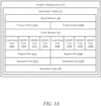
- FIG. 2B is a block diagram of a partition unit 220, according to an embodiment.
- the partition unit 220 is an instance of one of the partition units 220A-220N of Figure 2A .
- the partition unit 220 includes an L2 cache 221, a frame buffer interface 225, and a ROP 226 (raster operations unit).
- the L2 cache 221 is a read/write cache that is configured to perform load and store operations received from the memory crossbar 216 and ROP 226. Read misses and urgent write-back requests are output by L2 cache 221 to frame buffer interface 225 for processing. Dirty updates can also be sent to the frame buffer via the frame buffer interface 225 for opportunistic processing.
- the frame buffer interface 225 interfaces with one of the memory units in parallel processor memory, such as the memory units 224A-224N of Figure 2A (e.g., within parallel processor memory 222).
- the ROP 226 is a processing unit that performs raster operations, such as stencil, z test, blending, and the like. The ROP 226 then outputs processed graphics data that is stored in graphics memory.
- the ROP 226 includes compression logic to compress z or color data that is written to memory and decompress z or color data that is read from memory.
- the ROP 226 is included within each processing cluster (e.g., cluster 214A-214N of Figure 2A ) instead of within the partition unit 220. In such embodiment, read and write requests for pixel data are transmitted over the memory crossbar 216 instead of pixel fragment data.
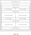
- FIG. 2C is a block diagram of a processing cluster 214 within a parallel processing unit, according to an embodiment.
- the processing cluster is an instance of one of the processing clusters 214A-214N of Figure 2A .
- the processing cluster 214 can be configured to execute many threads in parallel, where the term "thread” refers to an instance of a particular program executing on a particular set of input data.
- SIMD single-instruction, multiple-data
- SIMT single-instruction, multiple-thread
- Operation of the processing cluster 214 can be controlled via a pipeline manager 232 that distributes processing tasks to SIMT parallel processors.
- the pipeline manager 232 receives instructions from the scheduler 210 of Figure 2A and manages execution of those instructions via a graphics multiprocessor 234 and/or a texture unit 236.
- the illustrated graphics multiprocessor 234 is an exemplary instance of an SIMT parallel processor. However, various types of SIMT parallel processors of differing architectures may be included within the processing cluster 214.
- One or more instances of the graphics multiprocessor 234 can be included within a processing cluster 214.
- the graphics multiprocessor 234 can process data and a data crossbar 240 can be used to distribute the processed data to one of multiple possible destinations, including other shader units.
- the pipeline manager 232 can facilitate the distribution of processed data by specifying destinations for processed data to be distributed vis the data crossbar 240.
- Each graphics multiprocessor 234 within the processing cluster 214 can include an identical set of functional execution logic (e.g., arithmetic logic units, load-store units, etc.).
- the functional execution logic can be configured in a pipelined manner in which new instructions can be issued before previous instructions are complete.
- the functional execution logic may be provided.
- the functional logic supports a variety of operations including integer and floating point arithmetic comparison operations, Boolean operations bit-shifting, and computation of various algebraic functions.
- the same functional-unit hardware can be leveraged to perform different operations and any combination of functional units may be present.
- the instructions transmitted to the processing cluster 214 constitutes a thread.
- a set of threads executing across the set of parallel processing engines is a thread group.
- a thread group executes the same program on different input data.
- Each thread within a thread group can be assigned to a different processing engine within a graphics multiprocessor 234.
- a thread group may include fewer threads than the number of processing engines within the graphics multiprocessor 234. When a thread group includes fewer threads than the number of processing engines, one or more of the processing engines may be idle during cycles in which that thread group is being processed.
- a thread group may also include more threads than the number of processing engines within the graphics multiprocessor 234. When the thread group includes more threads than the number of processing engines within the graphics multiprocessor 234, processing can be performed over consecutive clock cycles. In one embodiment, multiple thread groups can be executed concurrently on a graphics multiprocessor 234.
- the graphics multiprocessor 234 includes an internal cache memory to perform load and store operations. In one embodiment, the graphics multiprocessor 234 can forego an internal cache and use a cache memory (e.g., L1 cache 308) within the processing cluster 214. Each graphics multiprocessor 234 also has access to L2 caches within the partition units (e.g., partition units 220A-220N of Figure 2A ) that are shared among all processing clusters 214 and may be used to transfer data between threads. The graphics multiprocessor 234 may also access off-chip global memory, which can include one or more of local parallel processor memory and/or system memory. Any memory external to the parallel processing unit 202 may be used as global memory. Embodiments in which the processing cluster 214 includes multiple instances of the graphics multiprocessor 234 can share common instructions and data, which may be stored in the L1 cache 308.
- L1 cache 308 e.g., L1 cache 308
- Each graphics multiprocessor 234 also has access to L2 caches within the partition units (e.g.
- Each processing cluster 214 may include an MMU 245 (memory management unit) that is configured to map virtual addresses into physical addresses.
- MMU 245 memory management unit
- the MMU 245 includes a set of page table entries (PTEs) used to map a virtual address to a physical address of a tile (talk more about tiling) and optionally a cache line index.
- PTEs page table entries
- the MMU 245 may include address translation lookaside buffers (TLB) or caches that may reside within the graphics multiprocessor 234 or the L1 cache or processing cluster 214.
- TLB address translation lookaside buffers
- the physical address is processed to distribute surface data access locality to allow efficient request interleaving among partition units.
- the cache line index may be used to determine whether a request for a cache line is a hit or miss.
- a processing cluster 214 may be configured such that each graphics multiprocessor 234 is coupled to a texture unit 236 for performing texture mapping operations, e.g., determining texture sample positions, reading texture data, and filtering the texture data.
- Texture data is read from an internal texture L1 cache (not shown) or in some embodiments from the L1 cache within graphics multiprocessor 234 and is fetched from an L2 cache, local parallel processor memory, or system memory, as needed.
- Each graphics multiprocessor 234 outputs processed tasks to the data crossbar 240 to provide the processed task to another processing cluster 214 for further processing or to store the processed task in an L2 cache, local parallel processor memory, or system memory via the memory crossbar 216.
- FIG. 2D shows a graphics multiprocessor 234, according to one embodiment.
- the graphics multiprocessor 234 couples with the pipeline manager 232 of the processing cluster 214.
- the graphics multiprocessor 234 has an execution pipeline including but not limited to an instruction cache 252, an instruction unit 254, an address mapping unit 256, a register file 258, one or more general purpose graphics processing unit (GPGPU) cores 262, and one or more load/store units 266.
- the GPGPU cores 262 and load/store units 266 are coupled with cache memory 272 and shared memory 270 via a memory and cache interconnect 268.
- the instruction cache 252 receives a stream of instructions to execute from the pipeline manager 232.
- the instructions are cached in the instruction cache 252 and dispatched for execution by the instruction unit 254.
- the instruction unit 254 can dispatch instructions as thread groups (e.g., warps), with each thread of the thread group assigned to a different execution unit within GPGPU core 262.
- An instruction can access any of a local, shared, or global address space by specifying an address within a unified address space.
- the address mapping unit 256 can be used to translate addresses in the unified address space into a distinct memory address that can be accessed by the load/store units 266.
- the register file 258 provides a set of registers for the functional units of the graphics multiprocessor 324.
- the register file 258 provides temporary storage for operands connected to the data paths of the functional units (e.g., GPGPU cores 262, load/store units 266) of the graphics multiprocessor 324.
- the register file 258 is divided between each of the functional units such that each functional unit is allocated a dedicated portion of the register file 258.
- the register file 258 is divided between the different warps being executed by the graphics multiprocessor 324.
- the GPGPU cores 262 can each include floating point units (FPUs) and/or integer arithmetic logic units (ALUs) that are used to execute instructions of the graphics multiprocessor 324.
- the GPGPU cores 262 can be similar in architecture or can differ in architecture, according to embodiments.
- a first portion of the GPGPU cores 262 include a single precision FPU and an integer ALU while a second portion of the GPGPU cores include a double precision FPU.
- the FPUs can implement the IEEE 754-2008 standard for floating point arithmetic or enable variable precision floating point arithmetic.
- the graphics multiprocessor 324 can additionally include one or more fixed function or special function units to perform specific functions such as copy rectangle or pixel blending operations.
- one or more of the GPGPU cores can also include fixed or special function logic.
- the memory and cache interconnect 268 is an interconnect network that connects each of the functional units of the graphics multiprocessor 324 to the register file 258 and to the shared memory 270.
- the memory and cache interconnect 268 is a crossbar interconnect that allows the load/store unit 266 to implement load and store operations between the shared memory 270 and the register file 258.
- the register file 258 can operate at the same frequency as the GPGPU cores 262, thus data transfer between the GPGPU cores 262 and the register file 258 is very low latency.
- the shared memory 270 can be used to enable communication between threads that execute on the functional units within the graphics multiprocessor 234.
- the cache memory 272 can be used as a data cache for example, to cache texture data communicated between the functional units and the texture unit 236.
- the shared memory 270 can also be used as a program managed cached. Threads executing on the GPGPU cores 262 can programmatically store data within the shared memory in addition to the automatically cached data that is stored within the cache memory 272.
- Figure 3A shows a graphics multiprocessor 325 according to an additional embodiment.
- the graphics multiprocessor 325 includes multiple additional instances of execution resource units relative to the graphics multiprocessor 234 of Figure 2D .
- the graphics multiprocessor 325 can include multiple instances of the instruction unit 332A-332B, register file 334A-334B, and texture unit(s) 344A-344B.
- the graphics multiprocessor 325 also includes multiple sets of graphics or compute execution units (e.g., GPGPU core 336A-336B, GPGPU core 337A-337B, GPGPU core 338A-338B) and multiple sets of load/store units 340A-340B.
- the execution resource units have a common instruction cache 330, texture and/or data cache memory 342, and shared memory 346.
- the various components can communicate via an interconnect fabric 327.
- the interconnect fabric 327 includes one or more crossbar switches to enable communication between the various components of the graphics multiprocessor 325.
- Figure 3B shows a graphics multiprocessor 350 according to an additional embodiment.
- the graphics processor includes multiple sets of execution resources 356A-356D, where each set of execution resource includes multiple instruction units, register files, GPGPU cores, and load store units, as illustrated in Figure 2D and Figure 3A .
- the execution resources 356A-356D can work in concert with texture unit(s) 360A-360D for texture operations, while sharing an instruction cache 354, and shared memory 362.
- the execution resources 356A-356D can share an instruction cache 354 and shared memory 362, as well as multiple instances of a texture and/or data cache memory 358A-358B.
- the various components can communicate via an interconnect fabric 352 similar to the interconnect fabric 327 of Figure 3A .
- FIG. 1 the architecture described in Figures 1 , 2A-2D , and 3A-3B are descriptive and not limiting as to the scope of the present embodiments.
- the techniques described herein may be implemented on any properly configured processing unit, including, without limitation, one or more mobile application processors, one or more desktop or server central processing units (CPUs) including multi-core CPUs, one or more parallel processing units, such as the parallel processing unit 202 of Figure 2A , as well as one or more graphics processors or special purpose processing units, without departure from the scope of the embodiments described herein.
- CPUs desktop or server central processing units
- parallel processing units such as the parallel processing unit 202 of Figure 2A
- graphics processors or special purpose processing units without departure from the scope of the embodiments described herein.
- the processor cores may allocate work to the GPU in the form of sequences of commands/instructions contained in a work descriptor.
- the GPU then uses dedicated circuitry/logic for efficiently processing these commands/instructions.
- Figure 4A illustrates an exemplary architecture in which a plurality of GPUs 410-413 are communicatively coupled to a plurality of multi-core processors 405-406 over high-speed links 440-443 (e.g., buses, point-to-point interconnects, etc.).
- the high-speed links 440-443 support a communication throughput of 4GB/s, 30GB/s, 80GB/s or higher, depending on the implementation.
- Various interconnect protocols may be used including, but not limited to, PCIe 4.0 or 5.0 and NVLink 2.0. However, the underlying principles of the specification are not limited to any particular communication protocol or throughput.
- two or more of the GPUs 410-413 are interconnected over high-speed links 444-445, which may be implemented using the same or different protocols/links than those used for high-speed links 440-443.
- two or more of the multi-core processors 405-406 may be connected over high speed link 433 which may be symmetric multi-processor (SMP) buses operating at 20GB/s, 30GB/s, 120GB/s or higher.
- SMP symmetric multi-processor
- each multi-core processor 405-406 is communicatively coupled to a processor memory 401-402, via memory interconnects 430-431, respectively, and each GPU 410-413 is communicatively coupled to GPU memory 420-423 over GPU memory interconnects 450-453, respectively.
- the memory interconnects 430-431 and 450-453 may utilize the same or different memory access technologies.
- the processor memories 401-402 and GPU memories 420-423 may be volatile memories such as dynamic random access memories (DRAMs) (including stacked DRAMs), Graphics DDR SDRAM (GDDR) (e.g., GDDR5, GDDR6), or High Bandwidth Memory (HBM) and/or may be non-volatile memories such as 3D XPoint or Nano-Ram.
- DRAMs dynamic random access memories
- GDDR Graphics DDR SDRAM
- HBM High Bandwidth Memory
- some portion of the memories may be volatile memory and another portion may be non-volatile memory (e.g., using a two-level memory (2LM) hierarchy).
- 2LM two-level memory
- processors 405-406 and GPUs 410-413 may be physically coupled to a particular memory 401-402, 420-423, respectively, a unified memory architecture may be implemented in which the same virtual system address space (also referred to as the "effective address" space) is distributed among all of the various physical memories.
- processor memories 401-402 may each comprise 64GB of the system memory address space
- GPU memories 420-423 may each comprise 32GB of the system memory address space (resulting in a total of 256GB addressable memory in this example).
- FIG. 4B illustrates additional details for an interconnection between a multi-core processor 407 and a graphics acceleration module 446 in accordance with one embodiment.
- the graphics acceleration module 446 may include one or more GPU chips integrated on a line card which is coupled to the processor 407 via the high-speed link 440.
- the graphics acceleration module 446 may be integrated on the same package or chip as the processor 407.
- the illustrated processor 407 includes a plurality of cores 460A-460D, each with a translation lookaside buffer 461A-461D and one or more caches 462A-462D.
- the cores may include various other components for executing instructions and processing data which are not illustrated to avoid obscuring the underlying principles of the specification (e.g., instruction fetch units, branch prediction units, decoders, execution units, reorder buffers, etc.).
- the caches 462A-462D may comprise level 1 (L1) and level 2 (L2) caches.
- one or more shared caches 426 may be included in the caching hierarchy and shared by sets of the cores 460A-460D.
- processor 407 includes 24 cores, each with its own L1 cache, twelve shared L2 caches, and twelve shared L3 caches. In this embodiment, one of the L2 and L3 caches are shared by two adjacent cores.
- the processor 407 and the graphics accelerator integration module 446 connect with system memory 441, which may include processor memories 401-402.
- a proxy circuit 425 communicatively couples the graphics acceleration module 446 to the coherence bus 464, allowing the graphics acceleration module 446 to participate in the cache coherence protocol as a peer of the cores.
- an interface 435 provides connectivity to the proxy circuit 425 over high-speed link 440 (e.g., a PCIe bus, NVLink, etc.) and an interface 437 connects the graphics acceleration module 446 to the link 440.
- high-speed link 440 e.g., a PCIe bus, NVLink, etc.
- an accelerator integration circuit 436 provides cache management, memory access, context management, and interrupt management services on behalf of a plurality of graphics processing engines 431, 432, N of the graphics acceleration module 446.
- the graphics processing engines 431, 432, N may each comprise a separate graphics processing unit (GPU).
- the graphics processing engines 431, 432, N may comprise different types of graphics processing engines within a GPU such as graphics execution units, media processing engines (e.g., video encoders/decoders), samplers, and blit engines.
- the graphics acceleration module may be a GPU with a plurality of graphics processing engines 431-432, N or the graphics processing engines 431-432, N may be individual GPUs integrated on a common package, line card, or chip.
- the accelerator integration circuit 436 includes a memory management unit (MMU) 439 for performing various memory management functions such as virtual-to-physical memory translations (also referred to as effective-to-real memory translations) and memory access protocols for accessing system memory 441.
- the MMU 439 may also include a translation lookaside buffer (TLB) (not shown) for caching the virtual/effective to physical/real address translations.
- a cache 438 stores commands and data for efficient access by the graphics processing engines 431-432, N.
- the data stored in cache 438 and graphics memories 433-434, N is kept coherent with the core caches 462A-462D, 456 and system memory 411.
- proxy circuit 425 which takes part in the cache coherency mechanism on behalf of cache 438 and memories 433-434, N (e.g., sending updates to the cache 438 related to modifications/accesses of cache lines on processor caches 462A-462D, 456 and receiving updates from the cache 438).
- a set of registers 445 store context data for threads executed by the graphics processing engines 431-432, N and a context management circuit 448 manages the thread contexts.
- the context management circuit 448 may perform save and restore operations to save and restore contexts of the various threads during contexts switches (e.g., where a first thread is saved and a second thread is stored so that the second thread can be execute by a graphics processing engine).
- the context management circuit 448 may store current register values to a designated region in memory (e.g., identified by a context pointer). It may then restore the register values when returning to the context.
- an interrupt management circuit 447 receives and processes interrupts received from system devices.
- the accelerator integration circuit acts as a bridge to the system for the graphics acceleration module 446 and provides address translation and system memory cache services.
- the accelerator integration circuit 436 may provide virtualization facilities for the host processor to manage virtualization of the graphics processing engines, interrupts, and memory management.
- one or more graphics memories 433-434, M are coupled to each of the graphics processing engines 431-432, N, respectively.
- the graphics memories 433-434, M store instructions and data being processed by each of the graphics processing engines 431-432, N.
- the graphics memories 433-434, M may be volatile memories such as DRAMs (including stacked DRAMs), GDDR memory (e.g., GDDR5, GDDR6), or HBM, and/or may be non-volatile memories such as 3D XPoint or Nano-Ram.
- the dedicated-process programming model is implementation-specific.
- a single process owns the graphics acceleration module 446 or an individual graphics processing engine 431. Because the graphics acceleration module 446 is owned by a single process, the hypervisor initializes the accelerator integration circuit 436 for the owning partition and the operating system initializes the accelerator integration circuit 436 for the owning process at the time when the graphics acceleration module 446 is assigned.
- the system hypervisor 496 owns the graphics acceleration module 446 and makes its function available to all operating systems 495.
- the graphics acceleration module 446 may adhere to the following requirements: 1) An application's job request must be autonomous (that is, the state does not need to be maintained between jobs), or the graphics acceleration module 446 must provide a context save and restore mechanism. 2) An application's job request is guaranteed by the graphics acceleration module 446 to complete in a specified amount of time, including any translation faults, or the graphics acceleration module 446 provides the ability to preempt the processing of the job. 3) The graphics acceleration module 446 must be guaranteed fairness between processes when operating in the directed shared programming model.
- the AMR value is the AMR state to use for the current process.
- the value passed to the operating system is similar to an application setting the AMR. If the accelerator integration circuit 436 and graphics acceleration module 446 implementations do not support a User Authority Mask Override Register (UAMOR), the operating system may apply the current UAMOR value to the AMR value before passing the AMR in the hypervisor call.
- the hypervisor 496 may optionally apply the current Authority Mask Override Register (AMOR) value before placing the AMR into the process element 483.
- the CSRP is one of the registers 445 containing the effective address of an area in the application's address space 482 for the graphics acceleration module 446 to save and restore the context state. This pointer is optional if no state is required to be saved between jobs or when a job is preempted.
- the context save/restore area may be pinned system memory.
- the operating system 495 may verify that the application 480 has registered and been given the authority to use the graphics acceleration module 446. The operating system 495 then calls the hypervisor 496 with the information shown in Table 3. Table 3 - OS to Hypervisor Call Parameters 1 A work descriptor (WD) 2 An Authority Mask Register (AMR) value (potentially masked). 3 An effective address (EA) Context Save/Restore Area Pointer (CSRP) 4 A process ID (PID) and optional thread ID (TID) 5 A virtual address (VA) accelerator utilization record pointer (AURP) 6 The virtual address of the storage segment table pointer (SSTP) 7 A logical interrupt service number (LISN)
- EA Context Save/Restore Area Pointer
- PID process ID
- TID thread ID
- VA accelerator utilization record pointer
- SSTP storage segment table pointer
- LISN logical interrupt service number
- SR state register
- LPID logical partition ID
- RA real address
- SDR Storage Descriptor Register
- one embodiment employs a unified memory addressable via a common virtual memory address space used to access the physical processor memories 401-402 and GPU memories 420-423.
- operations executed on the GPUs 410-413 utilize the same virtual/effective memory address space to access the processors memories 401-402 and vice versa, thereby simplifying programmability.
- a first portion of the virtual/effective address space is allocated to the processor memory 401, a second portion to the second processor memory 402, a third portion to the GPU memory 420, and so on.
- the entire virtual/effective memory space (sometimes referred to as the effective address space) is thereby distributed across each of the processor memories 401-402 and GPU memories 420-423, allowing any processor or GPU to access any physical memory with a virtual address mapped to that memory.
- GPU-attached memory 420-423 allows GPU-attached memory 420-423 to be mapped as part of system memory, and accessed using shared virtual memory (SVM) technology, but without suffering the typical performance drawbacks associated with full system cache coherence.
- SVM shared virtual memory
- the ability to GPU-attached memory 420-423 to be accessed as system memory without onerous cache coherence overhead provides a beneficial operating environment for GPU offload.
- This arrangement allows the host processor 405 software to setup operands and access computation results, without the overhead of tradition I/O DMA data copies. Such traditional copies involve driver calls, interrupts and memory mapped I/O (MMIO) accesses that are all inefficient relative to simple memory accesses.
- MMIO memory mapped I/O
- the ability to access GPU attached memory 420-423 without cache coherence overheads can be critical to the execution time of an offloaded computation.
- cache coherence overhead can significantly reduce the effective write bandwidth seen by a GPU 410-413.
- the efficiency of operand setup, the efficiency of results access, and the efficiency of GPU computation all play a role in determining the effectiveness of GPU offload.
- a second instance of a primitive assembler 514 receives vertex attributes from the tessellation evaluation processing unit 512, reading stored vertex attributes as needed, and constructs graphics primitives for processing by the geometry processing unit 516.
- the geometry processing unit 516 is a programmable execution unit that executes geometry shader programs to transform graphics primitives received from primitive assembler 514 as specified by the geometry shader programs.
- the geometry processing unit 516 is programmed to subdivide the graphics primitives into one or more new graphics primitives and calculate parameters used to rasterize the new graphics primitives.
- the rasterizer 522 can perform depth culling and other depth-based optimizations.
- the rasterizer 522 also performs scan conversion on the new graphics primitives to generate fragments and outputs those fragments and associated coverage data to the fragment/pixel processing unit 524.
- autonomous vehicle and “autonomous driving” are referenced throughout this document, embodiments are not limited as such.
- autonomous vehicle is not limed to an automobile but that it may include any number and type of autonomous machines, such as robots, autonomous equipment, household autonomous devices, and/or the like, and any one or more tasks or operations relating to such autonomous machines may be interchangeably referenced with autonomous driving.
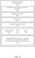
- Computing device 600 may include operating system (OS) 606 serving as an interface between hardware and/or physical resources of the computer device 600 and a user. It is contemplated that graphics processor 614 and application processor 612 may be one or more of processor(s) 102 of Figure 1 .
- OS operating system
- graphics processor 614 and application processor 612 may be one or more of processor(s) 102 of Figure 1 .
- Embodiments may be implemented as any or a combination of: one or more microchips or integrated circuits interconnected using a parentboard, hardwired logic, software stored by a memory device and executed by a microprocessor, firmware, an application specific integrated circuit (ASIC), and/or a field programmable gate array (FPGA).
- the terms “logic”, “module”, “component”, “engine”, and “mechanism” may include, by way of example, software or hardware and/or combinations of software and hardware.
- sharing and expansion mechanism 610 may be hosted or facilitated by operating system 606 of computing device 600.
- sharing and expansion mechanism 610 may be hosted by or part of graphics processing unit ("GPU” or simply “graphics processor") 614 or firmware of graphics processor 614.
- GPU graphics processing unit
- sharing and expansion mechanism 610 may be embedded in or implemented as part of the processing hardware of graphics processor 614.
- sharing and expansion mechanism 610 may be hosted by or part of central processing unit (“CPU” or simply “application processor”) 612.
- sharing and expansion mechanism 610 may be embedded in or implemented as part of the processing hardware of application processor 612.
- sharing and expansion mechanism 610 may be hosted by or part of any number and type of components of computing device 600, such as a portion of sharing and expansion mechanism 610 may be hosted by or part of operating system 606, another portion may be hosted by or part of graphics processor 614, another portion may be hosted by or part of application processor 612, while one or more portions of sharing and expansion mechanism 610 may be hosted by or part of operating system 606 and/or any number and type of devices of computing device 600. It is contemplated that one or more portions or components of sharing and expansion mechanism 610 may be employed as hardware, software, and/or firmware.
- embodiments may be downloaded as a computer program product, wherein the program may be transferred from a remote computer (e.g., a server) to a requesting computer (e.g., a client) by way of one or more data signals embodied in and/or modulated by a carrier wave or other propagation medium via a communication link (e.g., a modem and/or network connection).
- a remote computer e.g., a server
- a requesting computer e.g., a client
- a communication link e.g., a modem and/or network connection
- term “user” may be interchangeably referred to as “viewer”, “observer”, “person”, “individual”, “end-user”, and/or the like. It is to be noted that throughout this document, terms like “graphics domain” may be referenced interchangeably with “graphics processing unit”, “graphics processor”, or simply “GPU” and similarly, “CPU domain” or “host domain” may be referenced interchangeably with “computer processing unit”, “application processor”, or simply “CPU”.
- FIG. 7 illustrates sharing and expansion mechanism 610 of Figure 6 according to one embodiment.
- sharing and expansion mechanism 610 may include any number and type of components, such as (without limitations): detection/observation logic 701; library generation/mapping logic 703; data sharing/retrieval logic 705; communication/compatibility logic 707; and compression/expansion logic 709.
- data sharing is an efficient manner for having access to all the relevant data without going through long processes and procedures or re-inventing the wheel.
- conventional data sharing techniques are limited in their user as they do not provide for data sharing across processing systems, where one processing system can retrieve any portion of shared data if that portion is relevant to the work being performed by or at the processing system.
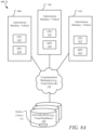
- Embodiments provide for a novel technique for offering to share data produced on any number and type of processing systems or devices, such as graphics processor 614, application processor 612, field programmable gate array (FPGA), application-specific integrated circuit (ASIC), and/or the like, using surface library.
- any processor working on the same convolution can retrieve data from the surface library, where this data had been produced by another processor.
- this data may be stored persistently across runs.
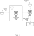
- detection/observation logic 701 may be used to detect and observe processors, such as graphics processor 614, as they work on, for example, convolution, where this information may be shared with sharing/retrieval logic 703 and library logic 705.
- graphics processor 614 may be facilitated by sharing/retrieval logic 703 to store the intermediate neural network (NN) data as data surface in surface library 731 located at one or more cloud databases or datacenters, such as database(s) 730, in communication with computing devices 600, 740 over one or more communication medium(s) 725, such as cloud network.
- CNN intermediate neural network
- library logic 703 may be used to generate one or more surface libraries, such as surface library 731, as desired or necessitated, as graphics processor 614 is detected by detection/observation logic 701 as working on the convolution and having data that is capable of being stored at surface library 731 and subsequently used by one or more other processing devices, such as application processor 612, application processor 742, graphics processor 744, etc.
- graphics processor 744 may access the intermediate NN data at surface library 731 as facilitated by sharing/retrieval logic 703.
- any surfaces produced in this matter may be optionally compressed by compression/expansion logic 709 for an even faster transmission time.
- shared surfaces as facilitated by shared library 731, may be used for cross-checking results by multiple deep learning systems, such as autonomous machines 600, 740 as further illustrated in Figure 8A .
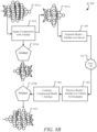
- Embodiments provide for a novel technique for compressing data models, while expanding them with an artefact to allow for smooth communication over communication medium(s) 725 without being costly, such as in terms of system or network resources, bandwidth, etc.
- compression/expansion logic 709 is be used to compress a data model and assign an artefact to the compressed model such that the artefact serves as both an extension to the compressed model and a form of identification if the compressed model is communicated from one machine 600 to another machine 740 over communication medium(s) 725.
- artefact or the use of artefact is merely according to one embodiment and that there may be other several techniques by which a compressed model may be re-combined to get the original model, such additional techniques may include (without limitation) using a "light” retraining within the vehicle, "hints" from peer vehicles/drivers, and/or the like.
- compression and expansion mechanism 610 any number and type of components may be added to and/or removed from compression and expansion mechanism 610 to facilitate various embodiments including adding, removing, and/or enhancing certain features.
- many of the standard and/or known components, such as those of a computing device, are not shown or discussed here. It is contemplated that embodiments, as described herein, are not limited to any particular technology, topology, system, architecture, and/or standard and are dynamic enough to adopt and adapt to any future changes.
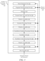
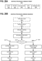
- Figure 9 illustrates a method 900 for facilitating data sharing across processing devices using surface library according to one embodiment.
- processing logic may comprise hardware (e.g., circuitry, dedicated logic, programmable logic, etc.), software (such as instructions run on a processing device), or a combination thereof, as facilitated by sharing and expansion mechanism 610 of Figure 6 .
- the processes associated with method 900 may be illustrated or recited in linear sequences for brevity and clarity in presentation; however, it is contemplated that any number of them can be performed in parallel, asynchronously, or in different orders.
- An exemplary type of machine learning algorithm is a neural network.
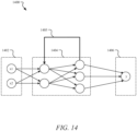
- a simple type of neural network is a feedforward network.
- a feedforward network may be implemented as an acyclic graph in which the nodes are arranged in layers.
- a feedforward network topology includes an input layer and an output layer that are separated by at least one hidden layer.
- the hidden layer transforms input received by the input layer into a representation that is useful for generating output in the output layer.
- the network nodes are fully connected via edges to the nodes in adjacent layers, but there are no edges between nodes within each layer.
- Figure 10 is a generalized diagram of a machine learning software stack 1000.
- a machine learning application 1002 can be configured to train a neural network using a training dataset or to use a trained deep neural network to implement machine intelligence.
- the machine learning application 1002 can include training and inference functionality for a neural network and/or specialized software that can be used to train a neural network before deployment.
- the machine learning application 1002 can implement any type of machine intelligence including but not limited to image recognition, mapping and localization, autonomous navigation, speech synthesis, medical imaging, or language translation.
- the GPGPU 1100 includes memory 1114A-B coupled with the compute clusters 1106A-H via a set of memory controllers 1112A-B.
- the memory 1114A-B can include various types of memory devices including dynamic random access memory (DRAM) or graphics random access memory, such as synchronous graphics random access memory (SGRAM), including graphics double data rate (GDDR) memory.
- DRAM dynamic random access memory
- SGRAM synchronous graphics random access memory
- GDDR graphics double data rate
- the memory units 224A-N may also include 3D stacked memory, including but not limited to high bandwidth memory (HBM).
- HBM high bandwidth memory
- the multiple instances of the GPGPU 1100 are located in separate data processing systems and communicate via a network device that is accessible via the host interface 1102.
- the GPU link 1110 can be configured to enable a connection to a host processor in addition to or as an alternative to the host interface 1102.
- the computing architecture provided by embodiments described herein can be configured to perform the types of parallel processing that is particularly suited for training and deploying neural networks for machine learning.
- a neural network can be generalized as a network of functions having a graph relationship. As is well-known in the art, there are a variety of types of neural network implementations used in machine learning.
- One exemplary type of neural network is the feedforward network, as previously described.
- a second exemplary type of neural network is the Convolutional Neural Network (CNN).
- CNN is a specialized feedforward neural network for processing data having a known, grid-like topology, such as image data. Accordingly, CNNs are commonly used for compute vision and image recognition applications, but they also may be used for other types of pattern recognition such as speech and language processing.
- the nodes in the CNN input layer are organized into a set of "filters" (feature detectors inspired by the receptive fields found in the retina), and the output of each set of filters is propagated to nodes in successive layers of the network.
- the computations for a CNN include applying the convolution mathematical operation to each filter to produce the output of that filter.
- Convolution is a specialized kind of mathematical operation performed by two functions to produce a third function that is a modified version of one of the two original functions.
- the first function to the convolution can be referred to as the input, while the second function can be referred to as the convolution kernel.
- the output may be referred to as the feature map.
- the input to a convolution layer can be a multidimensional array of data that defines the various color components of an input image.
- the convolution kernel can be a multidimensional array of parameters, where the parameters are adapted by the training process for the neural network.
- Deep learning is machine learning using deep neural networks.
- the deep neural networks used in deep learning are artificial neural networks composed of multiple hidden layers, as opposed to shallow neural networks that include only a single hidden layer. Deeper neural networks are generally more computationally intensive to train. However, the additional hidden layers of the network enable multistep pattern recognition that results in reduced output error relative to shallow machine learning techniques.
- Deep neural networks used in deep learning typically include a front-end network to perform feature recognition coupled to a back-end network which represents a mathematical model that can perform operations (e.g., object classification, speech recognition, etc.) based on the feature representation provided to the model.
- Deep learning enables machine learning to be performed without requiring hand crafted feature engineering to be performed for the model.
- deep neural networks can learn features based on statistical structure or correlation within the input data.
- the learned features can be provided to a mathematical model that can map detected features to an output.
- the mathematical model used by the network is generally specialized for the specific task to be performed, and different models will be used to perform different task.
- a learning model can be applied to the network to train the network to perform specific tasks.
- the learning model describes how to adjust the weights within the model to reduce the output error of the network.
- Backpropagation of errors is a common method used to train neural networks. An input vector is presented to the network for processing. The output of the network is compared to the desired output using a loss function and an error value is calculated for each of the neurons in the output layer. The error values are then propagated backwards until each neuron has an associated error value which roughly represents its contribution to the original output. The network can then learn from those errors using an algorithm, such as the stochastic gradient descent algorithm, to update the weights of the of the neural network.
- an algorithm such as the stochastic gradient descent algorithm
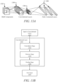
- Figure 13A-B illustrate an exemplary convolutional neural network.
- Figure 13A illustrates various layers within a CNN.
- an exemplary CNN used to model image processing can receive input 1302 describing the red, green, and blue (RGB) components of an input image.
- the input 1302 can be processed by multiple convolutional layers (e.g., convolutional layer 1304, convolutional layer 1306).
- the output from the multiple convolutional layers may optionally be processed by a set of fully connected layers 1308.
- Neurons in a fully connected layer have full connections to all activations in the previous layer, as previously described for a feedforward network.
- the output from the fully connected layers 1308 can be used to generate an output result from the network.
- the activations within the fully connected layers 1308 can be computed using matrix multiplication instead of convolution. Not all CNN implementations are make use of fully connected layers DPLA08. For example, in some implementations the convolutional layer 1306 can generate output for the CNN.
- the convolutional layers are sparsely connected, which differs from traditional neural network configuration found in the fully connected layers 1308.
- Traditional neural network layers are fully connected, such that every output unit interacts with every input unit.
- the convolutional layers are sparsely connected because the output of the convolution of a field is input (instead of the respective state value of each of the nodes in the field) to the nodes of the subsequent layer, as illustrated.
- the kernels associated with the convolutional layers perform convolution operations, the output of which is sent to the next layer.
- the dimensionality reduction performed within the convolutional layers is one aspect that enables the CNN to scale to process large images.
- Figure 13B illustrates exemplary computation stages within a convolutional layer of a CNN.
- Input to a convolutional layer 1312 of a CNN can be processed in three stages of a convolutional layer 1314.
- the three stages can include a convolution stage 1316, a detector stage 1318, and a pooling stage 1320.
- the convolution layer 1314 can then output data to a successive convolutional layer.
- the final convolutional layer of the network can generate output feature map data or provide input to a fully connected layer, for example, to generate a classification value for the input to the CNN.
- the convolution stage 1316 performs several convolutions in parallel to produce a set of linear activations.
- the convolution stage 1316 can include an affine transformation, which is any transformation that can be specified as a linear transformation plus a translation. Affine transformations include rotations, translations, scaling, and combinations of these transformations.
- the convolution stage computes the output of functions (e.g., neurons) that are connected to specific regions in the input, which can be determined as the local region associated with the neuron.
- the neurons compute a dot product between the weights of the neurons and the region in the local input to which the neurons are connected.
- the output from the convolution stage 1316 defines a set of linear activations that are processed by successive stages of the convolutional layer 1314.
- the linear activations can be processed by a detector stage 1318.
- each linear activation is processed by a non-linear activation function.
- the non-linear activation function increases the nonlinear properties of the overall network without affecting the receptive fields of the convolution layer.
- Non-linear activation functions may be used.
- ReLU rectified linear unit
- the pooling stage 1320 uses a pooling function that replaces the output of the convolutional layer 1306 with a summary statistic of the nearby outputs.
- the pooling function can be used to introduce translation invariance into the neural network, such that small translations to the input do not change the pooled outputs. Invariance to local translation can be useful in scenarios where the presence of a feature in the input data is more important than the precise location of the feature.
- Various types of pooling functions can be used during the pooling stage 1320, including max pooling, average pooling, and l2-norm pooling. Additionally, some CNN implementations do not include a pooling stage. Instead, such implementations substitute and additional convolution stage having an increased stride relative to previous convolution stages.
- the output from the convolutional layer 1314 can then be processed by the next layer 1322.
- the next layer 1322 can be an additional convolutional layer or one of the fully connected layers 1308.
- the first convolutional layer 1304 of Figure 13A can output to the second convolutional layer 1306, while the second convolutional layer can output to a first layer of the fully connected layers 1308.
- the initial weights may be chosen randomly or by pre-training using a deep belief network.
- the training cycle then be performed in either a supervised or unsupervised manner.
- Supervised learning is a learning method in which training is performed as a mediated operation, such as when the training dataset 1502 includes input paired with the desired output for the input, or where the training dataset includes input having known output and the output of the neural network is manually graded.
- the network processes the inputs and compares the resulting outputs against a set of expected or desired outputs. Errors are then propagated back through the system.
- the training framework 1504 can adjust to adjust the weights that control the untrained neural network 1506.
- the training framework 1504 can provide tools to monitor how well the untrained neural network 1506 is converging towards a model suitable to generating correct answers based on known input data.
- the training process occurs repeatedly as the weights of the network are adjusted to refine the output generated by the neural network.
- the training process can continue until the neural network reaches a statistically desired accuracy associated with a trained neural net 1508.
- the trained neural network 1508 can then be deployed to implement any number of machine learning operations.
- FIG 16 is a block diagram illustrating distributed learning.
- Distributed learning is a training model that uses multiple distributed computing nodes to perform supervised or unsupervised training of a neural network.
- the distributed computational nodes can each include one or more host processors and one or more of the general-purpose processing nodes, such as the highly-parallel general-purpose graphics processing unit 1100 as in Figure 1100.
- distributed learning can be performed model parallelism 1602, data parallelism 1604, or a combination of model and data parallelism 1604.
- Parallel processor accelerated machine learning can also be used to accelerate natural language processing.
- Automatic learning procedures can make use of statistical inference algorithms to produce models that are robust to erroneous or unfamiliar input.
- Exemplary natural language processor applications include automatic machine translation between human languages.
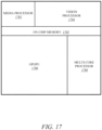
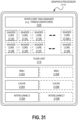
- FIG. 17 illustrates an exemplary inferencing system on a chip (SOC) 1700 suitable for performing inferencing using a trained model.
- the SOC 1700 can integrate processing components including a media processor 1702, a vision processor 1704, a GPGPU 1706 and a multi-core processor 1708.
- the SOC 1700 can additionally include on-chip memory 1705 that can enable a shared on-chip data pool that is accessible by each of the processing components.
- the processing components can be optimized for low power operation to enable deployment to a variety of machine learning platforms, including autonomous vehicles and autonomous robots.
- one implementation of the SOC 1700 can be used as a portion of the main control system for an autonomous vehicle. Where the SOC 1700 is configured for use in autonomous vehicles the SOC is designed and configured for compliance with the relevant functional safety standards of the deployment jurisdiction.
- the media processor 1702 and vision processor 1704 can work in concert to accelerate computer vision operations.
- the media processor 1702 can enable low latency decode of multiple high-resolution (e.g., 4K, 8K) video streams.
- the decoded video streams can be written to a buffer in the on-chip-memory 1705.
- the vision processor 1704 can then parse the decoded video and perform preliminary processing operations on the frames of the decoded video in preparation of processing the frames using a trained image recognition model.
- the vision processor 1704 can accelerate convolution operations for a CNN that is used to perform image recognition on the high-resolution video data, while back end model computations are performed by the GPGPU 1706.
- GPE 2110 couples with or includes a command streamer 2103, which provides a command stream to the 3D pipeline 2012 and/or media pipelines 2016.
- command streamer 2103 is coupled with memory, which can be system memory, or one or more of internal cache memory and shared cache memory.
- command streamer 2103 receives commands from the memory and sends the commands to 3D pipeline 2012 and/or media pipeline 2016.
- the commands are directives fetched from a ring buffer, which stores commands for the 3D pipeline 2012 and media pipeline 2016.
- the ring buffer can additionally include batch command buffers storing batches of multiple commands.
- Output data generated by threads executing on the graphics core array 2114 can output data to memory in a unified return buffer (URB) 2118.
- the URB 2118 can store data for multiple threads.
- the URB 2118 may be used to send data between different threads executing on the graphics core array 2114.
- the URB 2118 may additionally be used for synchronization between threads on the graphics core array and fixed function logic within the shared function logic 2120.
- graphics processor 2200 includes multiple graphics cores 2280A-2280N, each including a set of first sub-cores 2250A-2250N and a set of second sub-cores 2260A-2260N.
- Each sub-core in the set of first sub-cores 2250A-2250N includes at least a first set of execution units 2252A-2252N and media/texture samplers 2254A-2254N.
- Each sub-core in the set of second sub-cores 2260A-2260N includes at least a second set of execution units 2262A-2262N and samplers 2264A-2264N.
- each sub-core 2250A-2250N, 2260A-2260N shares a set of shared resources 2270A-2270N.
- the shared resources include shared cache memory and pixel operation logic. Other shared resources may also be included in the various embodiments of the graphics processor.
- execution unit array 2308A-2308N is primarily used to execute "shader" programs.
- the execution units in array 2308A-2308N execute an instruction set that includes native support for many standard 3D graphics shader instructions, such that shader programs from graphics libraries (e.g., Direct 3D and OpenGL) are executed with a minimal translation.
- the execution units support vertex and geometry processing (e.g., vertex programs, geometry programs, vertex shaders), pixel processing (e.g., pixel shaders, fragment shaders) and general-purpose processing (e.g., compute and media shaders).
- pixel shader 2302 is invoked to further compute output information and cause results to be written to output surfaces (e.g., color buffers, depth buffers, stencil buffers, etc.).
- pixel shader 2302 calculates the values of the various vertex attributes that are to be interpolated across the rasterized object.
- pixel shader 2302 then executes an application programming interface (API)-supplied pixel shader program.
- API application programming interface
- pixel shader 2302 dispatches threads to an execution unit (e.g., 2308A) via thread dispatcher 2304.
- the data port 2314 provides a memory access mechanism for the thread execution logic 2300 output processed data to memory for processing on a graphics processor output pipeline.
- the data port 2314 includes or couples to one or more cache memories (e.g., data cache 2312) to cache data for memory access via the data port.
- Figure 24 is a block diagram illustrating a graphics processor instruction formats 2400 according to some embodiments.
- the graphics processor execution units support an instruction set having instructions in multiple formats.
- the solid lined boxes illustrate the components that are generally included in an execution unit instruction, while the dashed lines include components that are optional or that are only included in a sub-set of the instructions.
- instruction format 2400 described and illustrated are macro-instructions, in that they are instructions supplied to the execution unit, as opposed to micro-operations resulting from instruction decode once the instruction is processed.
- instruction opcode 2412 defines the operation that the execution unit is to perform.
- the execution units execute each instruction in parallel across the multiple data elements of each operand. For example, in response to an add instruction the execution unit performs a simultaneous add operation across each color channel representing a texture element or picture element. By default, the execution unit performs each instruction across all data channels of the operands.
- instruction control field 2414 enables control over certain execution options, such as channels selection (e.g., predication) and data channel order (e.g., swizzle).
- channels selection e.g., predication
- data channel order e.g., swizzle
- exec-size field 2416 limits the number of data channels that will be executed in parallel. In some embodiments, exec-size field 2416 is not available for use in the 64-bit compact instruction format 2430.
- Some execution unit instructions have up to three operands including two source operands, src0 2420, src1 2422, and one destination 2418. In some embodiments, the execution units support dual destination instructions, where one of the destinations is implied.
- Data manipulation instructions can have a third source operand (e.g., SRC2 2424), where the instruction opcode 2412 determines the number of source operands.
- An instruction's last source operand can be an immediate (e.g., hard-coded) value passed with the instruction.
- the vector math group 2450 includes arithmetic instructions (e.g., dp4) in the form of 0101xxxxb (e.g., 0x50).
- the vector math group performs arithmetic such as dot product calculations on vector operands.
- render output pipeline 2570 contains a rasterizer and depth test component 2573 that converts vertex-based objects into an associated pixel-based representation.
- the render output pipeline 2570 includes a windower/masker unit to perform fixed function triangle and line rasterization.
- An associated render cache 2578 and depth cache 2579 are also available in some embodiments.
- a pixel operations component 2577 performs pixel-based operations on the data, though in some instances, pixel operations associated with 2D operations (e.g. bit block image transfers with blending) are performed by the 2D engine 2541, or substituted at display time by the display controller 2543 using overlay display planes.
- a shared L3 cache 2575 is available to all graphics components, allowing the sharing of data without the use of main system memory.
- graphics pipeline 2520 and media pipeline 2530 are configurable to perform operations based on multiple graphics and media programming interfaces and are not specific to any one application programming interface (API).
- driver software for the graphics processor translates API calls that are specific to a particular graphics or media library into commands that can be processed by the graphics processor.
- support is provided for the Open Graphics Library (OpenGL) and Open Computing Language (OpenCL) from the Khronos Group, the Direct3D library from the Microsoft Corporation, or support may be provided to both OpenGL and D3D. Support may also be provided for the Open Source Computer Vision Library (OpenCV).
- OpenGL Open Graphics Library
- OpenCL Open Computing Language
- Support may also be provided for the Open Source Computer Vision Library (OpenCV).
- OpenCV Open Source Computer Vision Library
- a future API with a compatible 3D pipeline would also be supported if a mapping can be made from the pipeline of the future API to the pipeline of the graphics processor.
- Figure 26A is a block diagram illustrating a graphics processor command format 2600 according to some embodiments.
- Figure 26B is a block diagram illustrating a graphics processor command sequence 2610 according to an embodiment.
- the solid lined boxes in Figure 26A illustrate the components that are generally included in a graphics command while the dashed lines include components that are optional or that are only included in a sub-set of the graphics commands.
- the exemplary graphics processor command format 2600 of Figure 26A includes data fields to identify a target client 2602 of the command, a command operation code (opcode) 2604, and the relevant data 2606 for the command.
- opcode command operation code
- a sub-opcode 2605 and a command size 2608 are also included in some commands.
- client 2602 specifies the client unit of the graphics device that processes the command data.
- a graphics processor command parser examines the client field of each command to condition the further processing of the command and route the command data to the appropriate client unit.
- the graphics processor client units include a memory interface unit, a render unit, a 2D unit, a 3D unit, and a media unit. Each client unit has a corresponding processing pipeline that processes the commands. Once the command is received by the client unit, the client unit reads the opcode 2604 and, if present, sub-opcode 2605 to determine the operation to perform. The client unit performs the command using information in data field 2606.
- an explicit command size 2608 is expected to specify the size of the command.
- the command parser automatically determines the size of at least some of the commands based on the command opcode.
- commands are aligned via multiples of a double word.
- the flow diagram in Figure 26B shows an exemplary graphics processor command sequence 2610.
- software or firmware of a data processing system that features an embodiment of a graphics processor uses a version of the command sequence shown to set up, execute, and terminate a set of graphics operations.
- a sample command sequence is shown and described for purposes of example only as embodiments are not limited to these specific commands or to this command sequence.
- the commands may be issued as batch of commands in a command sequence, such that the graphics processor will process the sequence of commands in at least partially concurrence.
- a pipeline select command 2613 is used when a command sequence requires the graphics processor to explicitly switch between pipelines. In some embodiments, a pipeline select command 2613 is required only once within an execution context before issuing pipeline commands unless the context is to issue commands for both pipelines. In some embodiments, a pipeline flush command is 2612 is required immediately before a pipeline switch via the pipeline select command 2613.
- a pipeline control command 2614 configures a graphics pipeline for operation and is used to program the 3D pipeline 2622 and the media pipeline 2624. In some embodiments, pipeline control command 2614 configures the pipeline state for the active pipeline. In one embodiment, the pipeline control command 2614 is used for pipeline synchronization and to clear data from one or more cache memories within the active pipeline before processing a batch of commands.
- the remaining commands in the command sequence differ based on the active pipeline for operations. Based on a pipeline determination 2620, the command sequence is tailored to the 3D pipeline 2622 beginning with the 3D pipeline state 2630, or the media pipeline 2624 beginning at the media pipeline state 2640.
- 3D pipeline 2622 is triggered via an execute 2634 command or event.
- a register write triggers command execution.
- execution is triggered via a 'go' or 'kick' command in the command sequence.
- command execution is triggered using a pipeline synchronization command to flush the command sequence through the graphics pipeline.
- the 3D pipeline will perform geometry processing for the 3D primitives. Once operations are complete, the resulting geometric objects are rasterized and the pixel engine colors the resulting pixels. Additional commands to control pixel shading and pixel back end operations may also be included for those operations.
- the graphics processor command sequence 2610 follows the media pipeline 2624 path when performing media operations.
- the specific use and manner of programming for the media pipeline 2624 depends on the media or compute operations to be performed. Specific media decode operations may be offloaded to the media pipeline during media decode.
- the media pipeline can also be bypassed and media decode can be performed in whole or in part using resources provided by one or more general-purpose processing cores.
- the media pipeline also includes elements for general-purpose graphics processor unit (GPGPU) operations, where the graphics processor is used to perform SIMD vector operations using computational shader programs that are not explicitly related to the rendering of graphics primitives.
- GPGPU general-purpose graphics processor unit
- operating system 2720 is a Microsoft ® Windows ® operating system from the Microsoft Corporation, a proprietary UNIX-like operating system, or an open source UNIX-like operating system using a variant of the Linux kernel.
- the operating system 2720 can support a graphics API 2722 such as the Direct3D API or the OpenGL API.
- the operating system 2720 uses a front-end shader compiler 2724 to compile any shader instructions 2712 in HLSL into a lower-level shader language.
- the compilation may be a just-in-time (JIT) compilation or the application can perform shader pre-compilation.
- high-level shaders are compiled into low-level shaders during the compilation of the 3D graphics application 2710.
- user mode graphics driver 2726 contains a back-end shader compiler 2727 to convert the shader instructions 2712 into a hardware specific representation.
- shader instructions 2712 in the GLSL high-level language are passed to a user mode graphics driver 2726 for compilation.
- user mode graphics driver 2726 uses operating system kernel mode functions 2728 to communicate with a kernel mode graphics driver 2729.
- kernel mode graphics driver 2729 communicates with graphics processor 2732 to dispatch commands and instructions.
- the RTL design 2815 or equivalent may be further synthesized by the design facility into a hardware model 2820, which may be in a hardware description language (HDL), or some other representation of physical design data.
- the HDL may be further simulated or tested to verify the IP core design.
- the IP core design can be stored for delivery to a 3 rd party fabrication facility 2865 using non-volatile memory 2840 (e.g., hard disk, flash memory, or any non-volatile storage medium).
- the IP core design may be transmitted (e.g., via the Internet) over a wired connection 2850 or wireless connection 2860.
- the fabrication facility 2865 may then fabricate an integrated circuit that is based at least in part on the IP core design.
- the fabricated integrated circuit can be configured to perform operations in accordance with at least one embodiment described herein.
- Graphics processor 3110 includes one or more shader core(s) 3115A-3115N (e.g., 3115A, 3115B, 3115C, 3115D, 3115E, 3115F, through 3015N-1, and 3015N), which provides for a unified shader core architecture in which a single core or type or core can execute all types of programmable shader code, including shader program code to implement vertex shaders, fragment shaders, and/or compute shaders. The exact number of shader cores present can vary among embodiments and implementations. Additionally, graphics processor 3110 includes an inter-core task manager 3105, which acts as a thread dispatcher to dispatch execution threads to one or more shader core(s) 3115A-3115N.
- shader core(s) 3115A-3115N e.g., 3115A, 3115B, 3115C, 3115D, 3115E, 3115F, through 3015N-1, and 3015N
- graphics processor 3110 includes an inter-core task manager 3105
- references to “one embodiment”, “an embodiment”, “example embodiment”, “various embodiments”, etc., indicate that the embodiment(s) so described may include particular features, structures, or characteristics, but not every embodiment necessarily includes the particular features, structures, or characteristics. Further, some embodiments may have some, all, or none of the features described for other embodiments.
Landscapes
- Engineering & Computer Science (AREA)
- Theoretical Computer Science (AREA)
- Physics & Mathematics (AREA)
- Software Systems (AREA)
- General Physics & Mathematics (AREA)
- General Engineering & Computer Science (AREA)
- Health & Medical Sciences (AREA)
- Life Sciences & Earth Sciences (AREA)
- Biomedical Technology (AREA)
- Biophysics (AREA)
- General Health & Medical Sciences (AREA)
- Molecular Biology (AREA)
- Computing Systems (AREA)
- Evolutionary Computation (AREA)
- Data Mining & Analysis (AREA)
- Mathematical Physics (AREA)
- Computational Linguistics (AREA)
- Artificial Intelligence (AREA)
- Neurology (AREA)
- Computer Networks & Wireless Communication (AREA)
- Signal Processing (AREA)
- Image Processing (AREA)
- Image Generation (AREA)
Claims (7)
- Einrichtung (600), die konfiguriert ist zum Vereinfachen eines gemeinsamen Nutzens von Daten und einer Komprimierung/Erweiterung von Datenmodellen, wobei die Einrichtung umfasst:eine Erkennungs-/Beobachtungslogik (701), die konfiguriert ist zum Erkennen eines ersten Prozessors, der Informationen verarbeitet, die sich auf ein neuronales Netzwerk in der Einrichtung beziehen, wobei das neuronale Netzwerk ein neuronales Faltungsnetzwerk (Convolutional Neural Network, CNN) beinhaltet und wobei der erste Prozessor einen ersten Grafikprozessor (614) umfasst und wobei die Einrichtung (600) eine erste autonome Maschine umfasst; undeine Logik zum gemeinsamen Nutzen und Abrufen von Daten (705), die konfiguriert ist zum Vereinfachen eines Speicherns, durch den ersten Prozessor, von Daten eines zwischengeschalteten neuronalen Netzwerks, NN, in einer Bibliothek (731) in einer Datenbank (730), wobei die Daten des zwischengeschalteten NN für einen zweiten Prozessor einer Computervorrichtung (740) über ein oder mehrere Kommunikationsmedien zugänglich sind,wobei die Logik zum gemeinsamen Nutzen und Abrufen von Daten (705) konfiguriert ist zum Vereinfachen eines Zugreifens und Abrufens, durch den zweiten Prozessor, der Daten des zwischengeschalteten NN aus der Bibliothek (731), wenn der zweite Prozessor Aufgaben in Bezug auf das neuronale Netzwerk durchführt, wobei der zweite Prozessor einen zweiten Grafikprozessor umfasst und wobei die Computervorrichtung eine zweite autonome Maschine umfasst,und ferner eine Komprimierungs-/Erweiterungslogik (709) umfasst, die konfiguriert ist zum Komprimieren der Daten des zwischengeschalteten NN, indem ein Artefakt angewandt wird und wobei das Artefakt und eine Kombination der komprimierten Daten des zwischengeschalteten NN zusammen mit dem Artefakt über das eine oder die mehreren Kommunikationsmedien (725) zu der zweiten autonomen Maschine kommuniziert werden, wobei das Artefakt sowohl als eine Erweiterung für die komprimierten Daten des zwischengeschalteten NN als auch als eine Form einer Identifizierung dient, wobei die Komprimierungs-/Erweiterungslogik (709) ferner konfiguriert ist zum Vereinfachen eines Empfangs des Artefakts und der Kombination der komprimierten Daten des zwischengeschalteten NN und des Artefakts in der zweiten autonomen Maschine, wobei die komprimierten Daten des zwischengeschalteten NN unter Verwendung des Artefakts dekomprimiert werden.
- Einrichtung nach Anspruch 1, die ferner eine Bibliothekserzeugungs-/-zuordnungslogik (703) umfasst, die konfiguriert ist zum Erzeugen der Bibliothek (731) in der Datenbank (730), wobei die Bibliothekserzeugungs-/-zuordnungslogik (703) ferner konfiguriert ist zum Zuordnen der Daten des zwischengeschalteten NN zu dem ersten Prozessor, wobei die erste und die zweite autonome Maschine autonome Fahrzeuge in einer Kommunikation über ein oder mehrere Kommunikationsmedien (725) beinhalten, wobei die Datenbank (730) eine Cloud-Datenbank beinhaltet.
- Einrichtung nach Anspruch 1, wobei der erste Grafikprozessor (614) zusammen mit einem Anwendungsprozessor (612) in einem gemeinsamen Halbleitergehäuse angeordnet ist.
- Verfahren zum Vereinfachen eines gemeinsamen Nutzens von Daten und einer Komprimierung/Erweiterung von Datenmodellen, wobei das Verfahren umfasst:Erkennen eines ersten Prozessors, der Informationen verarbeitet, die sich auf ein neuronales Netzwerk in einer ersten Computervorrichtung (600) beziehen, wobei das neuronale Netzwerk ein neuronales Faltungsnetzwerk (Convolutional Neural Network, CNN) beinhaltet und wobei der erste Prozessor einen ersten Grafikprozessor (614) umfasst und wobei die erste Computervorrichtung (600) eine erste autonome Maschine umfasst; undVereinfachen eines Speicherns, durch den ersten Prozessor, von Daten eines zwischengeschalteten neuronalen Netzwerks, NN, in einer Oberflächenbibliothek (731) in einer Datenbank (730), wobei die Daten des zwischengeschalteten NN für einen zweiten Prozessor einer Computervorrichtung (740) über ein oder mehrere Kommunikationsmedien zugänglich sind,und das ferner ein Vereinfachen eines Zugreifens und Abrufens, durch den zweiten Prozessor, der Daten des zwischengeschalteten NN aus der Oberflächenbibliothek (731) umfasst, wenn der zweite Prozessor Aufgaben in Bezug auf das neuronale Netzwerk durchführt, wobei der zweite Prozessor einen zweiten Grafikprozessor (744) umfasst und wobei die Computervorrichtung (740) eine zweite autonome Maschine umfasst, und das ferner ein Komprimieren der Daten des zwischengeschalteten NN umfasst, indem ein Artefakt angewandt wird und wobei das Artefakt und eine Kombination der komprimierten Daten des zwischengeschalteten NN zusammen mit dem Artefakt über das eine oder die mehreren Kommunikationsmedien (725) zu der zweiten autonomen Maschine kommuniziert werden, und wobei die komprimierten Daten des zwischengeschalteten NN unter Verwendung des Artefakts dekomprimiert werden, wobei das Artefakt sowohl als eine Erweiterung für die komprimierten Daten des zwischengeschalteten NN als auch als eine Form einer Identifizierung dient.
- Verfahren nach Anspruch 4, das außerdem mindestens eines umfasst von:Erzeugen der Bibliothek (731) in der Datenbank (730); und/oderZuordnen der Daten der zwischengeschalteten NN zu dem ersten Prozessor, wobei die erste und die zweite autonome Maschine autonome Fahrzeuge in einer Kommunikation über ein oder mehrere Kommunikationsmedien (725) beinhalten, wobei die Datenbank (730) eine Cloud-Datenbank beinhaltet.
- Verfahren nach Anspruch 4, das ferner ein Vereinfachen eines Empfangs der komprimierten Daten des zwischengeschalteten NN und des Artefakt in der zweiten autonomen Maschine umfasst, wobei der erste Grafikprozessor (614) zusammen mit einem Anwendungsprozessor (612) in einem gemeinsamen Halbleitergehäuse angeordnet ist.
- Mindestens ein maschinenlesbares Medium, das eine Vielzahl von Anweisungen umfasst, die, wenn sie in einer Computervorrichtung ausgeführt werden, zum Implementieren oder Durchführen eines Verfahrens nach einem der Ansprüche 4 bis 6 dienen.
Applications Claiming Priority (1)
| Application Number | Priority Date | Filing Date | Title |
|---|---|---|---|
| US15/495,081 US10497084B2 (en) | 2017-04-24 | 2017-04-24 | Efficient sharing and compression expansion of data across processing systems |
Publications (2)
| Publication Number | Publication Date |
|---|---|
| EP3396544A1 EP3396544A1 (de) | 2018-10-31 |
| EP3396544B1 true EP3396544B1 (de) | 2024-07-03 |
Family
ID=61965665
Family Applications (1)
| Application Number | Title | Priority Date | Filing Date |
|---|---|---|---|
| EP18163725.7A Active EP3396544B1 (de) | 2017-04-24 | 2018-03-23 | Effizientes teilen und komprimieren von daten über verarbeitungssysteme hinweg |
Country Status (5)
| Country | Link |
|---|---|
| US (3) | US10497084B2 (de) |
| EP (1) | EP3396544B1 (de) |
| CN (1) | CN108734646A (de) |
| ES (1) | ES2993162T3 (de) |
| PL (1) | PL3396544T3 (de) |
Families Citing this family (27)
| Publication number | Priority date | Publication date | Assignee | Title |
|---|---|---|---|---|
| US10497084B2 (en) | 2017-04-24 | 2019-12-03 | Intel Corporation | Efficient sharing and compression expansion of data across processing systems |
| US11006184B2 (en) * | 2018-05-16 | 2021-05-11 | Quantum Radius Corporation | Enhanced distribution image system |
| US10636484B2 (en) * | 2018-09-12 | 2020-04-28 | Winbond Electronics Corporation | Circuit and method for memory operation |
| CN109377778B (zh) * | 2018-11-15 | 2021-04-06 | 浪潮集团有限公司 | 一种基于多路rdma和v2x的协同自动驾驶系统及方法 |
| US11520331B2 (en) * | 2018-12-28 | 2022-12-06 | Intel Corporation | Methods and apparatus to update autonomous vehicle perspectives |
| US11353870B2 (en) * | 2018-12-31 | 2022-06-07 | Baidu Usa Llc | Autonomous driving computing and storage expansion device with flexible host and client configuration |
| WO2020146007A1 (en) * | 2019-01-09 | 2020-07-16 | Futurewei Technologies, Inc. | Machine learning network model compression |
| US11625487B2 (en) * | 2019-01-24 | 2023-04-11 | International Business Machines Corporation | Framework for certifying a lower bound on a robustness level of convolutional neural networks |
| KR102425039B1 (ko) * | 2019-02-27 | 2022-07-28 | 한국전력공사 | 분산 딥러닝 환경에서 데이터 압축 장치 및 방법 |
| US11444845B1 (en) * | 2019-03-05 | 2022-09-13 | Amazon Technologies, Inc. | Processing requests using compressed and complete machine learning models |
| CN110349087B (zh) * | 2019-07-08 | 2021-02-12 | 华南理工大学 | 基于适应性卷积的rgb-d图像高质量网格生成方法 |
| US12249189B2 (en) | 2019-08-12 | 2025-03-11 | Micron Technology, Inc. | Predictive maintenance of automotive lighting |
| US11586194B2 (en) * | 2019-08-12 | 2023-02-21 | Micron Technology, Inc. | Storage and access of neural network models of automotive predictive maintenance |
| US12061971B2 (en) | 2019-08-12 | 2024-08-13 | Micron Technology, Inc. | Predictive maintenance of automotive engines |
| US12497055B2 (en) | 2019-08-21 | 2025-12-16 | Micron Technology, Inc. | Monitoring controller area network bus for vehicle control |
| US11042350B2 (en) | 2019-08-21 | 2021-06-22 | Micron Technology, Inc. | Intelligent audio control in vehicles |
| US12210401B2 (en) | 2019-09-05 | 2025-01-28 | Micron Technology, Inc. | Temperature based optimization of data storage operations |
| CN112749120B (zh) * | 2019-10-29 | 2024-09-20 | 辉达公司 | 将数据有效地传输至处理器的技术 |
| CN111062419B (zh) * | 2019-11-26 | 2023-06-02 | 复旦大学 | 一种深度学习数据集的压缩和恢复方法 |
| US11250648B2 (en) | 2019-12-18 | 2022-02-15 | Micron Technology, Inc. | Predictive maintenance of automotive transmission |
| CN113297128B (zh) * | 2020-02-24 | 2023-10-31 | 中科寒武纪科技股份有限公司 | 数据处理方法、装置、计算机设备和存储介质 |
| US11848980B2 (en) * | 2020-07-09 | 2023-12-19 | Boray Data Technology Co. Ltd. | Distributed pipeline configuration in a distributed computing system |
| KR20220013231A (ko) | 2020-07-24 | 2022-02-04 | 삼성전자주식회사 | 영상 내에서 객체를 추론하는 전자 장치 및 추론 방법 |
| US11557292B1 (en) * | 2020-10-21 | 2023-01-17 | Amazon Technologies, Inc. | Speech command verification |
| US11556381B2 (en) * | 2021-05-07 | 2023-01-17 | Google Llc | Asynchronous distributed data flow for machine learning workloads |
| US12175006B2 (en) | 2021-09-09 | 2024-12-24 | Bank Of America Corporation | System for electronic data artifact testing using a hybrid centralized-decentralized computing platform |
| US12204917B2 (en) * | 2022-12-14 | 2025-01-21 | Sap Se | Automated extensibility framework |
Citations (3)
| Publication number | Priority date | Publication date | Assignee | Title |
|---|---|---|---|---|
| EP1569128A2 (de) * | 2003-12-09 | 2005-08-31 | Microsoft Corporation | System und Verfahren zur Beschleunigung und Optimierung von Verarbeitung von Maschinenlehrtechniken unter Verwendung einer graphische Verarbeitungseinheit |
| US20100079454A1 (en) * | 2008-09-29 | 2010-04-01 | Legakis Justin S | Single Pass Tessellation |
| US20170024641A1 (en) * | 2015-07-22 | 2017-01-26 | Qualcomm Incorporated | Transfer learning in neural networks |
Family Cites Families (23)
| Publication number | Priority date | Publication date | Assignee | Title |
|---|---|---|---|---|
| CA2335561A1 (en) * | 2000-05-31 | 2001-11-30 | Frank J. Degilio | Heterogeneous client server method, system and program product for a partitioned processing environment |
| US7266532B2 (en) | 2001-06-01 | 2007-09-04 | The General Hospital Corporation | Reconfigurable autonomous device networks |
| US7873812B1 (en) | 2004-04-05 | 2011-01-18 | Tibet MIMAR | Method and system for efficient matrix multiplication in a SIMD processor architecture |
| CA2549417C (en) * | 2006-03-22 | 2011-09-20 | Accenture S.P.A. | Messaging interface between telecommunications service provider processing systems |
| US8533550B2 (en) * | 2010-06-29 | 2013-09-10 | Intel Corporation | Method and system to improve the performance and/or reliability of a solid-state drive |
| CN102271156A (zh) * | 2011-07-20 | 2011-12-07 | 武汉爱迪智能工程有限公司 | 基于物联网的数据共享服务系统 |
| DE102012009876A1 (de) * | 2011-11-10 | 2013-05-16 | Audi Ag | Verfahren zum Verarbeiten einer Bildsequenz und Testgerät für einen Kraftwagen |
| US9304570B2 (en) * | 2011-12-15 | 2016-04-05 | Intel Corporation | Method, apparatus, and system for energy efficiency and energy conservation including power and performance workload-based balancing between multiple processing elements |
| US9913330B2 (en) * | 2012-06-15 | 2018-03-06 | Lightel Technologies, Inc. | Solid-state lighting operable with compact fluorescent ballasts and AC mains |
| US9582287B2 (en) * | 2012-09-27 | 2017-02-28 | Intel Corporation | Processor having multiple cores, shared core extension logic, and shared core extension utilization instructions |
| KR101992274B1 (ko) * | 2013-01-02 | 2019-09-30 | 삼성전자주식회사 | 데이터 압축 방법과 상기 방법을 수행할 수 있는 장치들 |
| CN103530224A (zh) * | 2013-06-26 | 2014-01-22 | 郑州大学 | 一种基于GPU的Harris角点检测软件系统 |
| CN104200095B (zh) * | 2014-08-28 | 2017-05-10 | 南京大学 | 基于感知进化神经网络的传感信道可扩展系统及其方法 |
| US10223333B2 (en) | 2014-08-29 | 2019-03-05 | Nvidia Corporation | Performing multi-convolution operations in a parallel processing system |
| US10223635B2 (en) * | 2015-01-22 | 2019-03-05 | Qualcomm Incorporated | Model compression and fine-tuning |
| US10114618B2 (en) * | 2015-06-08 | 2018-10-30 | Cisco Technology, Inc. | Autonomous mobile sensor movement path simulation with an integrated developer environment |
| US20170136881A1 (en) * | 2015-11-13 | 2017-05-18 | NextEv USA, Inc. | Vehicle to vehicle charging system and method of use |
| US10373019B2 (en) * | 2016-01-13 | 2019-08-06 | Ford Global Technologies, Llc | Low- and high-fidelity classifiers applied to road-scene images |
| US10997496B2 (en) | 2016-08-11 | 2021-05-04 | Nvidia Corporation | Sparse convolutional neural network accelerator |
| US10891538B2 (en) | 2016-08-11 | 2021-01-12 | Nvidia Corporation | Sparse convolutional neural network accelerator |
| US10254766B2 (en) * | 2016-11-09 | 2019-04-09 | Walmart Apollo, Llc | Autonomous ganged vehicles |
| US10592725B2 (en) * | 2017-04-21 | 2020-03-17 | General Electric Company | Neural network systems |
| US10497084B2 (en) | 2017-04-24 | 2019-12-03 | Intel Corporation | Efficient sharing and compression expansion of data across processing systems |
-
2017
- 2017-04-24 US US15/495,081 patent/US10497084B2/en active Active
-
2018
- 2018-03-23 PL PL18163725.7T patent/PL3396544T3/pl unknown
- 2018-03-23 ES ES18163725T patent/ES2993162T3/es active Active
- 2018-03-23 EP EP18163725.7A patent/EP3396544B1/de active Active
- 2018-04-23 CN CN201810368865.1A patent/CN108734646A/zh active Pending
-
2019
- 2019-11-26 US US16/696,852 patent/US11049213B2/en active Active
-
2021
- 2021-06-23 US US17/355,267 patent/US11669932B2/en active Active
Patent Citations (3)
| Publication number | Priority date | Publication date | Assignee | Title |
|---|---|---|---|---|
| EP1569128A2 (de) * | 2003-12-09 | 2005-08-31 | Microsoft Corporation | System und Verfahren zur Beschleunigung und Optimierung von Verarbeitung von Maschinenlehrtechniken unter Verwendung einer graphische Verarbeitungseinheit |
| US20100079454A1 (en) * | 2008-09-29 | 2010-04-01 | Legakis Justin S | Single Pass Tessellation |
| US20170024641A1 (en) * | 2015-07-22 | 2017-01-26 | Qualcomm Incorporated | Transfer learning in neural networks |
Also Published As
| Publication number | Publication date |
|---|---|
| EP3396544A1 (de) | 2018-10-31 |
| US11049213B2 (en) | 2021-06-29 |
| US20180308203A1 (en) | 2018-10-25 |
| PL3396544T3 (pl) | 2024-11-12 |
| US11669932B2 (en) | 2023-06-06 |
| CN108734646A (zh) | 2018-11-02 |
| US20200202480A1 (en) | 2020-06-25 |
| US20210390654A1 (en) | 2021-12-16 |
| US10497084B2 (en) | 2019-12-03 |
| ES2993162T3 (en) | 2024-12-23 |
Similar Documents
| Publication | Publication Date | Title |
|---|---|---|
| US11669932B2 (en) | Efficient sharing and compression expansion of data across processing systems | |
| US20240280987A1 (en) | Barriers and synchronization for machine learning at autonomous machines | |
| US10871966B2 (en) | Intelligent thread dispatch and vectorization of atomic operations | |
| EP3764314B1 (de) | Sparse-computation-mechanismus für maschinelles lernen | |
| EP3955203B1 (de) | Koordination und erhöhte nutzung von grafikprozessoren während der inferenz | |
| US11748106B2 (en) | Data operations and finite state machine for machine learning via bypass of computational tasks based on frequently-used data values | |
| US11592817B2 (en) | Storage management for machine learning at autonomous machines | |
| US20210350215A1 (en) | Training with adaptive runtime and precision profiling | |
| EP3396546A1 (de) | Berechnungsoptimierungsmechanismus für tiefe neuronale netzwerke | |
| EP3385844A1 (de) | Planungsmechanismus für neuronales netzwerk | |
| EP3396532B1 (de) | Dynamische präzision für rechenoperationen neuronaler netzwerke | |
| EP3396599A1 (de) | Hardware-optimiertes neuronales faltungsnetzwerk | |
| WO2018176435A1 (en) | Execution unit-shared hybrid technique for accelerated computing on graphics processors | |
| EP3944076A1 (de) | Variable präzision und mischungsdarstellung mehrerer schichten in einem netzwerk | |
| EP3396623B1 (de) | Echtzeitkontextabhängiges tiefenlernen |
Legal Events
| Date | Code | Title | Description |
|---|---|---|---|
| PUAI | Public reference made under article 153(3) epc to a published international application that has entered the european phase |
Free format text: ORIGINAL CODE: 0009012 |
|
| STAA | Information on the status of an ep patent application or granted ep patent |
Free format text: STATUS: THE APPLICATION HAS BEEN PUBLISHED |
|
| AK | Designated contracting states |
Kind code of ref document: A1 Designated state(s): AL AT BE BG CH CY CZ DE DK EE ES FI FR GB GR HR HU IE IS IT LI LT LU LV MC MK MT NL NO PL PT RO RS SE SI SK SM TR |
|
| AX | Request for extension of the european patent |
Extension state: BA ME |
|
| STAA | Information on the status of an ep patent application or granted ep patent |
Free format text: STATUS: REQUEST FOR EXAMINATION WAS MADE |
|
| 17P | Request for examination filed |
Effective date: 20190411 |
|
| RBV | Designated contracting states (corrected) |
Designated state(s): AL AT BE BG CH CY CZ DE DK EE ES FI FR GB GR HR HU IE IS IT LI LT LU LV MC MK MT NL NO PL PT RO RS SE SI SK SM TR |
|
| STAA | Information on the status of an ep patent application or granted ep patent |
Free format text: STATUS: EXAMINATION IS IN PROGRESS |
|
| 17Q | First examination report despatched |
Effective date: 20200122 |
|
| GRAP | Despatch of communication of intention to grant a patent |
Free format text: ORIGINAL CODE: EPIDOSNIGR1 |
|
| STAA | Information on the status of an ep patent application or granted ep patent |
Free format text: STATUS: GRANT OF PATENT IS INTENDED |
|
| INTG | Intention to grant announced |
Effective date: 20240205 |
|
| GRAS | Grant fee paid |
Free format text: ORIGINAL CODE: EPIDOSNIGR3 |
|
| GRAA | (expected) grant |
Free format text: ORIGINAL CODE: 0009210 |
|
| STAA | Information on the status of an ep patent application or granted ep patent |
Free format text: STATUS: THE PATENT HAS BEEN GRANTED |
|
| AK | Designated contracting states |
Kind code of ref document: B1 Designated state(s): AL AT BE BG CH CY CZ DE DK EE ES FI FR GB GR HR HU IE IS IT LI LT LU LV MC MK MT NL NO PL PT RO RS SE SI SK SM TR |
|
| REG | Reference to a national code |
Ref country code: CH Ref legal event code: EP |
|
| REG | Reference to a national code |
Ref country code: DE Ref legal event code: R096 Ref document number: 602018071203 Country of ref document: DE |
|
| P01 | Opt-out of the competence of the unified patent court (upc) registered |
Free format text: CASE NUMBER: APP_36828/2024 Effective date: 20240620 |
|
| REG | Reference to a national code |
Ref country code: NL Ref legal event code: FP |
|
| REG | Reference to a national code |
Ref country code: LT Ref legal event code: MG9D |
|
| PG25 | Lapsed in a contracting state [announced via postgrant information from national office to epo] |
Ref country code: PT Free format text: LAPSE BECAUSE OF FAILURE TO SUBMIT A TRANSLATION OF THE DESCRIPTION OR TO PAY THE FEE WITHIN THE PRESCRIBED TIME-LIMIT Effective date: 20241104 |
|
| REG | Reference to a national code |
Ref country code: AT Ref legal event code: MK05 Ref document number: 1700549 Country of ref document: AT Kind code of ref document: T Effective date: 20240703 |
|
| REG | Reference to a national code |
Ref country code: ES Ref legal event code: FG2A Ref document number: 2993162 Country of ref document: ES Kind code of ref document: T3 Effective date: 20241223 |
|
| PG25 | Lapsed in a contracting state [announced via postgrant information from national office to epo] |
Ref country code: PT Free format text: LAPSE BECAUSE OF FAILURE TO SUBMIT A TRANSLATION OF THE DESCRIPTION OR TO PAY THE FEE WITHIN THE PRESCRIBED TIME-LIMIT Effective date: 20241104 |
|
| PG25 | Lapsed in a contracting state [announced via postgrant information from national office to epo] |
Ref country code: NO Free format text: LAPSE BECAUSE OF FAILURE TO SUBMIT A TRANSLATION OF THE DESCRIPTION OR TO PAY THE FEE WITHIN THE PRESCRIBED TIME-LIMIT Effective date: 20241003 |
|
| PG25 | Lapsed in a contracting state [announced via postgrant information from national office to epo] |
Ref country code: GR Free format text: LAPSE BECAUSE OF FAILURE TO SUBMIT A TRANSLATION OF THE DESCRIPTION OR TO PAY THE FEE WITHIN THE PRESCRIBED TIME-LIMIT Effective date: 20241004 Ref country code: FI Free format text: LAPSE BECAUSE OF FAILURE TO SUBMIT A TRANSLATION OF THE DESCRIPTION OR TO PAY THE FEE WITHIN THE PRESCRIBED TIME-LIMIT Effective date: 20240703 |
|
| PGFP | Annual fee paid to national office [announced via postgrant information from national office to epo] |
Ref country code: NL Payment date: 20241203 Year of fee payment: 8 |
|
| PG25 | Lapsed in a contracting state [announced via postgrant information from national office to epo] |
Ref country code: BG Free format text: LAPSE BECAUSE OF FAILURE TO SUBMIT A TRANSLATION OF THE DESCRIPTION OR TO PAY THE FEE WITHIN THE PRESCRIBED TIME-LIMIT Effective date: 20240703 |
|
| PGFP | Annual fee paid to national office [announced via postgrant information from national office to epo] |
Ref country code: FR Payment date: 20241129 Year of fee payment: 8 |
|
| PG25 | Lapsed in a contracting state [announced via postgrant information from national office to epo] |
Ref country code: LV Free format text: LAPSE BECAUSE OF FAILURE TO SUBMIT A TRANSLATION OF THE DESCRIPTION OR TO PAY THE FEE WITHIN THE PRESCRIBED TIME-LIMIT Effective date: 20240703 |
|
| PG25 | Lapsed in a contracting state [announced via postgrant information from national office to epo] |
Ref country code: IS Free format text: LAPSE BECAUSE OF FAILURE TO SUBMIT A TRANSLATION OF THE DESCRIPTION OR TO PAY THE FEE WITHIN THE PRESCRIBED TIME-LIMIT Effective date: 20241103 Ref country code: AT Free format text: LAPSE BECAUSE OF FAILURE TO SUBMIT A TRANSLATION OF THE DESCRIPTION OR TO PAY THE FEE WITHIN THE PRESCRIBED TIME-LIMIT Effective date: 20240703 |
|
| PG25 | Lapsed in a contracting state [announced via postgrant information from national office to epo] |
Ref country code: CZ Free format text: LAPSE BECAUSE OF FAILURE TO SUBMIT A TRANSLATION OF THE DESCRIPTION OR TO PAY THE FEE WITHIN THE PRESCRIBED TIME-LIMIT Effective date: 20240703 Ref country code: HR Free format text: LAPSE BECAUSE OF FAILURE TO SUBMIT A TRANSLATION OF THE DESCRIPTION OR TO PAY THE FEE WITHIN THE PRESCRIBED TIME-LIMIT Effective date: 20240703 |
|
| PG25 | Lapsed in a contracting state [announced via postgrant information from national office to epo] |
Ref country code: RS Free format text: LAPSE BECAUSE OF FAILURE TO SUBMIT A TRANSLATION OF THE DESCRIPTION OR TO PAY THE FEE WITHIN THE PRESCRIBED TIME-LIMIT Effective date: 20241003 |
|
| PG25 | Lapsed in a contracting state [announced via postgrant information from national office to epo] |
Ref country code: RS Free format text: LAPSE BECAUSE OF FAILURE TO SUBMIT A TRANSLATION OF THE DESCRIPTION OR TO PAY THE FEE WITHIN THE PRESCRIBED TIME-LIMIT Effective date: 20241003 Ref country code: NO Free format text: LAPSE BECAUSE OF FAILURE TO SUBMIT A TRANSLATION OF THE DESCRIPTION OR TO PAY THE FEE WITHIN THE PRESCRIBED TIME-LIMIT Effective date: 20241003 Ref country code: LV Free format text: LAPSE BECAUSE OF FAILURE TO SUBMIT A TRANSLATION OF THE DESCRIPTION OR TO PAY THE FEE WITHIN THE PRESCRIBED TIME-LIMIT Effective date: 20240703 Ref country code: IS Free format text: LAPSE BECAUSE OF FAILURE TO SUBMIT A TRANSLATION OF THE DESCRIPTION OR TO PAY THE FEE WITHIN THE PRESCRIBED TIME-LIMIT Effective date: 20241103 Ref country code: HR Free format text: LAPSE BECAUSE OF FAILURE TO SUBMIT A TRANSLATION OF THE DESCRIPTION OR TO PAY THE FEE WITHIN THE PRESCRIBED TIME-LIMIT Effective date: 20240703 Ref country code: GR Free format text: LAPSE BECAUSE OF FAILURE TO SUBMIT A TRANSLATION OF THE DESCRIPTION OR TO PAY THE FEE WITHIN THE PRESCRIBED TIME-LIMIT Effective date: 20241004 Ref country code: FI Free format text: LAPSE BECAUSE OF FAILURE TO SUBMIT A TRANSLATION OF THE DESCRIPTION OR TO PAY THE FEE WITHIN THE PRESCRIBED TIME-LIMIT Effective date: 20240703 Ref country code: CZ Free format text: LAPSE BECAUSE OF FAILURE TO SUBMIT A TRANSLATION OF THE DESCRIPTION OR TO PAY THE FEE WITHIN THE PRESCRIBED TIME-LIMIT Effective date: 20240703 Ref country code: BG Free format text: LAPSE BECAUSE OF FAILURE TO SUBMIT A TRANSLATION OF THE DESCRIPTION OR TO PAY THE FEE WITHIN THE PRESCRIBED TIME-LIMIT Effective date: 20240703 Ref country code: AT Free format text: LAPSE BECAUSE OF FAILURE TO SUBMIT A TRANSLATION OF THE DESCRIPTION OR TO PAY THE FEE WITHIN THE PRESCRIBED TIME-LIMIT Effective date: 20240703 |
|
| REG | Reference to a national code |
Ref country code: DE Ref legal event code: R097 Ref document number: 602018071203 Country of ref document: DE |
|
| PGFP | Annual fee paid to national office [announced via postgrant information from national office to epo] |
Ref country code: DE Payment date: 20250218 Year of fee payment: 8 |
|
| PG25 | Lapsed in a contracting state [announced via postgrant information from national office to epo] |
Ref country code: DK Free format text: LAPSE BECAUSE OF FAILURE TO SUBMIT A TRANSLATION OF THE DESCRIPTION OR TO PAY THE FEE WITHIN THE PRESCRIBED TIME-LIMIT Effective date: 20240703 Ref country code: RO Free format text: LAPSE BECAUSE OF FAILURE TO SUBMIT A TRANSLATION OF THE DESCRIPTION OR TO PAY THE FEE WITHIN THE PRESCRIBED TIME-LIMIT Effective date: 20240703 Ref country code: SM Free format text: LAPSE BECAUSE OF FAILURE TO SUBMIT A TRANSLATION OF THE DESCRIPTION OR TO PAY THE FEE WITHIN THE PRESCRIBED TIME-LIMIT Effective date: 20240703 |
|
| PG25 | Lapsed in a contracting state [announced via postgrant information from national office to epo] |
Ref country code: EE Free format text: LAPSE BECAUSE OF FAILURE TO SUBMIT A TRANSLATION OF THE DESCRIPTION OR TO PAY THE FEE WITHIN THE PRESCRIBED TIME-LIMIT Effective date: 20240703 |
|
| PGFP | Annual fee paid to national office [announced via postgrant information from national office to epo] |
Ref country code: PL Payment date: 20250228 Year of fee payment: 8 |
|
| PG25 | Lapsed in a contracting state [announced via postgrant information from national office to epo] |
Ref country code: SK Free format text: LAPSE BECAUSE OF FAILURE TO SUBMIT A TRANSLATION OF THE DESCRIPTION OR TO PAY THE FEE WITHIN THE PRESCRIBED TIME-LIMIT Effective date: 20240703 |
|
| PGFP | Annual fee paid to national office [announced via postgrant information from national office to epo] |
Ref country code: GB Payment date: 20250220 Year of fee payment: 8 Ref country code: IT Payment date: 20250226 Year of fee payment: 8 |
|
| PLBE | No opposition filed within time limit |
Free format text: ORIGINAL CODE: 0009261 |
|
| STAA | Information on the status of an ep patent application or granted ep patent |
Free format text: STATUS: NO OPPOSITION FILED WITHIN TIME LIMIT |
|
| 26N | No opposition filed |
Effective date: 20250404 |
|
| PGFP | Annual fee paid to national office [announced via postgrant information from national office to epo] |
Ref country code: ES Payment date: 20250410 Year of fee payment: 8 |
|
| PG25 | Lapsed in a contracting state [announced via postgrant information from national office to epo] |
Ref country code: SE Free format text: LAPSE BECAUSE OF FAILURE TO SUBMIT A TRANSLATION OF THE DESCRIPTION OR TO PAY THE FEE WITHIN THE PRESCRIBED TIME-LIMIT Effective date: 20240703 |
|
| PG25 | Lapsed in a contracting state [announced via postgrant information from national office to epo] |
Ref country code: MC Free format text: LAPSE BECAUSE OF FAILURE TO SUBMIT A TRANSLATION OF THE DESCRIPTION OR TO PAY THE FEE WITHIN THE PRESCRIBED TIME-LIMIT Effective date: 20240703 |
|
| REG | Reference to a national code |
Ref country code: CH Ref legal event code: H13 Free format text: ST27 STATUS EVENT CODE: U-0-0-H10-H13 (AS PROVIDED BY THE NATIONAL OFFICE) Effective date: 20251023 |
|
| PG25 | Lapsed in a contracting state [announced via postgrant information from national office to epo] |
Ref country code: LU Free format text: LAPSE BECAUSE OF NON-PAYMENT OF DUE FEES Effective date: 20250323 |
|
| REG | Reference to a national code |
Ref country code: BE Ref legal event code: MM Effective date: 20250331 |
|
| PG25 | Lapsed in a contracting state [announced via postgrant information from national office to epo] |
Ref country code: BE Free format text: LAPSE BECAUSE OF NON-PAYMENT OF DUE FEES Effective date: 20250331 |
|
| PG25 | Lapsed in a contracting state [announced via postgrant information from national office to epo] |
Ref country code: CH Free format text: LAPSE BECAUSE OF NON-PAYMENT OF DUE FEES Effective date: 20250331 |
|
| PG25 | Lapsed in a contracting state [announced via postgrant information from national office to epo] |
Ref country code: IE Free format text: LAPSE BECAUSE OF NON-PAYMENT OF DUE FEES Effective date: 20250323 |