EP3395783A1 - Method for producing a sintered joint between a ceramic substrate and a carrier - Google Patents
Method for producing a sintered joint between a ceramic substrate and a carrier Download PDFInfo
- Publication number
- EP3395783A1 EP3395783A1 EP17168793.2A EP17168793A EP3395783A1 EP 3395783 A1 EP3395783 A1 EP 3395783A1 EP 17168793 A EP17168793 A EP 17168793A EP 3395783 A1 EP3395783 A1 EP 3395783A1
- Authority
- EP
- European Patent Office
- Prior art keywords
- carrier
- layer
- powder
- ceramic substrate
- substrate
- Prior art date
- Legal status (The legal status is an assumption and is not a legal conclusion. Google has not performed a legal analysis and makes no representation as to the accuracy of the status listed.)
- Granted
Links
Images


Classifications
-
- C—CHEMISTRY; METALLURGY
- C04—CEMENTS; CONCRETE; ARTIFICIAL STONE; CERAMICS; REFRACTORIES
- C04B—LIME, MAGNESIA; SLAG; CEMENTS; COMPOSITIONS THEREOF, e.g. MORTARS, CONCRETE OR LIKE BUILDING MATERIALS; ARTIFICIAL STONE; CERAMICS; REFRACTORIES; TREATMENT OF NATURAL STONE
- C04B37/00—Joining burned ceramic articles with other burned ceramic articles or other articles by heating
- C04B37/02—Joining burned ceramic articles with other burned ceramic articles or other articles by heating with metallic articles
- C04B37/023—Joining burned ceramic articles with other burned ceramic articles or other articles by heating with metallic articles characterised by the interlayer used
- C04B37/026—Joining burned ceramic articles with other burned ceramic articles or other articles by heating with metallic articles characterised by the interlayer used consisting of metals or metal salts
-
- C—CHEMISTRY; METALLURGY
- C04—CEMENTS; CONCRETE; ARTIFICIAL STONE; CERAMICS; REFRACTORIES
- C04B—LIME, MAGNESIA; SLAG; CEMENTS; COMPOSITIONS THEREOF, e.g. MORTARS, CONCRETE OR LIKE BUILDING MATERIALS; ARTIFICIAL STONE; CERAMICS; REFRACTORIES; TREATMENT OF NATURAL STONE
- C04B35/00—Shaped ceramic products characterised by their composition; Ceramics compositions; Processing powders of inorganic compounds preparatory to the manufacturing of ceramic products
- C04B35/622—Forming processes; Processing powders of inorganic compounds preparatory to the manufacturing of ceramic products
- C04B35/626—Preparing or treating the powders individually or as batches ; preparing or treating macroscopic reinforcing agents for ceramic products, e.g. fibres; mechanical aspects section B
- C04B35/62605—Treating the starting powders individually or as mixtures
- C04B35/62645—Thermal treatment of powders or mixtures thereof other than sintering
- C04B35/6268—Thermal treatment of powders or mixtures thereof other than sintering characterised by the applied pressure or type of atmosphere, e.g. in vacuum, hydrogen or a specific oxygen pressure
-
- C—CHEMISTRY; METALLURGY
- C04—CEMENTS; CONCRETE; ARTIFICIAL STONE; CERAMICS; REFRACTORIES
- C04B—LIME, MAGNESIA; SLAG; CEMENTS; COMPOSITIONS THEREOF, e.g. MORTARS, CONCRETE OR LIKE BUILDING MATERIALS; ARTIFICIAL STONE; CERAMICS; REFRACTORIES; TREATMENT OF NATURAL STONE
- C04B2235/00—Aspects relating to ceramic starting mixtures or sintered ceramic products
- C04B2235/60—Aspects relating to the preparation, properties or mechanical treatment of green bodies or pre-forms
- C04B2235/604—Pressing at temperatures other than sintering temperatures
-
- C—CHEMISTRY; METALLURGY
- C04—CEMENTS; CONCRETE; ARTIFICIAL STONE; CERAMICS; REFRACTORIES
- C04B—LIME, MAGNESIA; SLAG; CEMENTS; COMPOSITIONS THEREOF, e.g. MORTARS, CONCRETE OR LIKE BUILDING MATERIALS; ARTIFICIAL STONE; CERAMICS; REFRACTORIES; TREATMENT OF NATURAL STONE
- C04B2237/00—Aspects relating to ceramic laminates or to joining of ceramic articles with other articles by heating
- C04B2237/02—Aspects relating to interlayers, e.g. used to join ceramic articles with other articles by heating
- C04B2237/12—Metallic interlayers
- C04B2237/125—Metallic interlayers based on noble metals, e.g. silver
-
- C—CHEMISTRY; METALLURGY
- C04—CEMENTS; CONCRETE; ARTIFICIAL STONE; CERAMICS; REFRACTORIES
- C04B—LIME, MAGNESIA; SLAG; CEMENTS; COMPOSITIONS THEREOF, e.g. MORTARS, CONCRETE OR LIKE BUILDING MATERIALS; ARTIFICIAL STONE; CERAMICS; REFRACTORIES; TREATMENT OF NATURAL STONE
- C04B2237/00—Aspects relating to ceramic laminates or to joining of ceramic articles with other articles by heating
- C04B2237/50—Processing aspects relating to ceramic laminates or to the joining of ceramic articles with other articles by heating
- C04B2237/52—Pre-treatment of the joining surfaces, e.g. cleaning, machining
- C04B2237/525—Pre-treatment of the joining surfaces, e.g. cleaning, machining by heating
-
- C—CHEMISTRY; METALLURGY
- C04—CEMENTS; CONCRETE; ARTIFICIAL STONE; CERAMICS; REFRACTORIES
- C04B—LIME, MAGNESIA; SLAG; CEMENTS; COMPOSITIONS THEREOF, e.g. MORTARS, CONCRETE OR LIKE BUILDING MATERIALS; ARTIFICIAL STONE; CERAMICS; REFRACTORIES; TREATMENT OF NATURAL STONE
- C04B2237/00—Aspects relating to ceramic laminates or to joining of ceramic articles with other articles by heating
- C04B2237/50—Processing aspects relating to ceramic laminates or to the joining of ceramic articles with other articles by heating
- C04B2237/55—Pre-treatments of a coated or not coated substrate other than oxidation treatment in order to form an active joining layer
-
- C—CHEMISTRY; METALLURGY
- C04—CEMENTS; CONCRETE; ARTIFICIAL STONE; CERAMICS; REFRACTORIES
- C04B—LIME, MAGNESIA; SLAG; CEMENTS; COMPOSITIONS THEREOF, e.g. MORTARS, CONCRETE OR LIKE BUILDING MATERIALS; ARTIFICIAL STONE; CERAMICS; REFRACTORIES; TREATMENT OF NATURAL STONE
- C04B2237/00—Aspects relating to ceramic laminates or to joining of ceramic articles with other articles by heating
- C04B2237/50—Processing aspects relating to ceramic laminates or to the joining of ceramic articles with other articles by heating
- C04B2237/56—Using constraining layers before or during sintering
-
- C—CHEMISTRY; METALLURGY
- C04—CEMENTS; CONCRETE; ARTIFICIAL STONE; CERAMICS; REFRACTORIES
- C04B—LIME, MAGNESIA; SLAG; CEMENTS; COMPOSITIONS THEREOF, e.g. MORTARS, CONCRETE OR LIKE BUILDING MATERIALS; ARTIFICIAL STONE; CERAMICS; REFRACTORIES; TREATMENT OF NATURAL STONE
- C04B2237/00—Aspects relating to ceramic laminates or to joining of ceramic articles with other articles by heating
- C04B2237/50—Processing aspects relating to ceramic laminates or to the joining of ceramic articles with other articles by heating
- C04B2237/62—Forming laminates or joined articles comprising holes, channels or other types of openings
-
- H—ELECTRICITY
- H10—SEMICONDUCTOR DEVICES; ELECTRIC SOLID-STATE DEVICES NOT OTHERWISE PROVIDED FOR
- H10W—GENERIC PACKAGES, INTERCONNECTIONS, CONNECTORS OR OTHER CONSTRUCTIONAL DETAILS OF DEVICES COVERED BY CLASS H10
- H10W40/00—Arrangements for thermal protection or thermal control
- H10W40/20—Arrangements for cooling
- H10W40/25—Arrangements for cooling characterised by their materials
- H10W40/255—Arrangements for cooling characterised by their materials having a laminate or multilayered structure, e.g. direct bond copper [DBC] ceramic substrates
-
- H—ELECTRICITY
- H10—SEMICONDUCTOR DEVICES; ELECTRIC SOLID-STATE DEVICES NOT OTHERWISE PROVIDED FOR
- H10W—GENERIC PACKAGES, INTERCONNECTIONS, CONNECTORS OR OTHER CONSTRUCTIONAL DETAILS OF DEVICES COVERED BY CLASS H10
- H10W72/00—Interconnections or connectors in packages
- H10W72/50—Bond wires
- H10W72/531—Shapes of wire connectors
- H10W72/5363—Shapes of wire connectors the connected ends being wedge-shaped
-
- H—ELECTRICITY
- H10—SEMICONDUCTOR DEVICES; ELECTRIC SOLID-STATE DEVICES NOT OTHERWISE PROVIDED FOR
- H10W—GENERIC PACKAGES, INTERCONNECTIONS, CONNECTORS OR OTHER CONSTRUCTIONAL DETAILS OF DEVICES COVERED BY CLASS H10
- H10W72/00—Interconnections or connectors in packages
- H10W72/851—Dispositions of multiple connectors or interconnections
- H10W72/874—On different surfaces
- H10W72/884—Die-attach connectors and bond wires
-
- H—ELECTRICITY
- H10—SEMICONDUCTOR DEVICES; ELECTRIC SOLID-STATE DEVICES NOT OTHERWISE PROVIDED FOR
- H10W—GENERIC PACKAGES, INTERCONNECTIONS, CONNECTORS OR OTHER CONSTRUCTIONAL DETAILS OF DEVICES COVERED BY CLASS H10
- H10W90/00—Package configurations
- H10W90/701—Package configurations characterised by the relative positions of pads or connectors relative to package parts
- H10W90/731—Package configurations characterised by the relative positions of pads or connectors relative to package parts of die-attach connectors
- H10W90/734—Package configurations characterised by the relative positions of pads or connectors relative to package parts of die-attach connectors between a chip and a stacked insulating package substrate, interposer or RDL
-
- H—ELECTRICITY
- H10—SEMICONDUCTOR DEVICES; ELECTRIC SOLID-STATE DEVICES NOT OTHERWISE PROVIDED FOR
- H10W—GENERIC PACKAGES, INTERCONNECTIONS, CONNECTORS OR OTHER CONSTRUCTIONAL DETAILS OF DEVICES COVERED BY CLASS H10
- H10W90/00—Package configurations
- H10W90/701—Package configurations characterised by the relative positions of pads or connectors relative to package parts
- H10W90/751—Package configurations characterised by the relative positions of pads or connectors relative to package parts of bond wires
- H10W90/754—Package configurations characterised by the relative positions of pads or connectors relative to package parts of bond wires between a chip and a stacked insulating package substrate, interposer or RDL
Definitions
- the instant disclosure relates to a method for producing a sintered joint between a ceramic substrate and a carrier.
- Ceramic substrates are widely used as circuit boards in power electronic modules or other electronic assemblies. Compared with conventional non-ceramic printed circuit boards, ceramic substrates can withstand high temperatures, exhibit high thermal conductivities and have high insulation strengths. In order to mechanically stabilize the ceramic substrate and/or to improve the dissipation of heat generated by an electronic component mounted on the ceramic substrate, the ceramic substrates are frequently joined with a carrier using a substance bond, e.g. by soldering. However, it has been shown that cracks in the ceramic layer of a ceramic substrate joined with a carrier can occur during the production of a composite that includes a ceramic substrate joined with a carrier.
- a need has been identified for a method for forming a substance-bond between a ceramic substrate and a carrier that prevents or at least reduces the risk of cracks in the ceramic layer of the ceramic substrate.
- a method for producing a sintered joint between a ceramic substrate and a carrier includes pre-heating the carrier by increasing a temperature of the carrier from an initial temperature to at least a first threshold temperature.
- a pressure, with which the pre-heated carrier, the ceramic substrate and a powder-including layer disposed between the pre-heated carrier and the ceramic substrate are pressed against one another, is increased from an initial pressure of less than or equal to an initial pressure threshold to at least a first pressure threshold, and the powder-including layer is sintered by simultaneously keeping the pressure for at least a minimum sintering time at at least the first pressure threshold and the temperature of the carrier at at least the first temperature threshold so that the powder-including layer is converted into a joining layer joining the carrier and the ceramic substrate.
- the first temperature threshold is a temperature which allows for sintering the powder-including layer when it is heated to that temperature.
- an exemplary electronic assembly 100 includes a composite with a carrier 1, a ceramic substrate 2, and a first joining layer 41 joining the carrier 1 and the ceramic substrate 2.
- the ceramic substrate 2 includes a dielectric ceramic layer 20, an optional first substrate metallization layer 21 and an optional second substrate metallization layer 22.
- the first substrate metallization layer 21 and the second substrate metallization layer 22 are attached to opposite surfaces of the ceramic layer 20.
- the second substrate metallization layer 22 may be patterned to include at least two conductor tracks 221, 222 disposed distant from one another.
- the dielectric ceramic layer 20 may be made of any dielectric ceramic material, e.g. alumina (Al 2 O 3 ), aluminum nitride (AlN) or silicon nitride (Si 3 N 4 ), so that it can provide for an electrical insulation between the first substrate metallization layer 21 and the second substrate metallization layer 22, or at least for an electrical insulation between a conductor track formed in the first substrate metallization layer 21 and a further conductor track formed in the second substrate metallization layer 22. If it is desired that the ceramic layer 20 electrically insulates the first substrate metallization layer 21 from the second substrate metallization layer 22, it may be free of electrically conductive vias. Alternatively, however, the ceramic layer 20 of a ceramic substrate 2 may include one or more electrically conductive vias electrically connecting the first substrate metallization layer 21 and the second substrate metallization layer 22.
- alumina Al 2 O 3
- AlN aluminum nitride
- Si 3 N 4 silicon nitride
- the first substrate metallization layer 21 and the second substrate metallization layer 22 may include any metal, e.g. copper or aluminum, or metal alloy and be attached to opposite surfaces of the ceramic layer 20 using any joining technique, e.g. brazing, direct copper bonding (DCB) or direct aluminum bonding (DAB).
- the first substrate metallization layer 21 may include a thin coating, for example in order to improve the sinterability.
- the second substrate metallization layer 22 may, at its side facing away from the ceramic layer 20, include a thin coating, for example in order to improve the solderability or the sinterability, or to protect the second substrate metallization layer 22 against oxidation.
- a suitable coating for improving the solderability is, e.g., a layer consisting of or including Ni
- a suitable coating for improving the sinterability is, e.g., a layer consisting of or including a noble metal, e.g., Ag or Au or Pd.
- the carrier 1 serves to mechanically stabilize the ceramic substrate 2.
- the carrier 1 may have, without being restricted to, a thickness d2 of at least 2 mm.
- the carrier 1 may consist of or include metal.
- the substrate 1 may include at least 95 weight% copper or at least 95 weight% aluminum, or it may consist of or include a metal-matrix-composite (MMC) material like aluminum silicon carbide or any other MMC-material.
- MMC metal-matrix-composite
- the first joining layer 41 adjoins both the carrier 1 and the ceramic substrate 2 and causes a substance-to-substance bond between the carrier 1 and the ceramic substrate 2.
- the first joining layer 41 is formed by sintering a powder during a sintering process which includes a pressing and temperature process.
- an electronic component 3 Disposed on that side of the second substrate metallization layer 22 facing away from the ceramic layer 20 is an electronic component 3, e.g. a power semiconductor chip.
- An example of an electronic component 3 formed as a power semiconductor chip is illustrated in Figure 1 .
- the power semiconductor chip includes a semiconductor body 30, a first chip metallization layer 31 and a second chip metallization layer 32.
- a second joining layer 42 creating a substance-to-substance bond between the ceramic substrate 2 and the electronic component 3 adjoins both the ceramic substrate 2 (e.g. that surface of the second metallization layer 22 facing away from the ceramic layer 20) and the electronic component 3 (here: that surface of the second chip metallization layer 32 facing away from the semiconductor body 30).
- the second joining layer 42 may be a solder layer, a layer including a sintered metal powder, or a layer of an electrically conductive or electrically insulating adhesive.
- a bonding wire 5 is, at a first bonding location 51, wire bonded to the first chip metallization layer 31, and, at a second bonding location 52, to the second substrate metallization layer 22.
- the semiconductor chip 3 may be mounted on a first conductor track 221 formed in the second substrate metallization layer 22 (so that the second joining layer 42 adjoins the first conductor track 221 and joins the semiconductor chip 3 to the ceramic substrate 2 at the first conductor track 221).
- the first bonding location 51 may be a location at the first chip metallization layer 31
- the second bonding location 52 may be a location at a second conductor track 222 formed in the second substrate metallization layer 22.
- Figure 2 illustrates the carrier 1 and the ceramic substrate 2 prior to being joined.
- a powder-including layer 41' may be applied to that surface of the first substrate metallization layer 21 facing away from the ceramic layer 20, and/or a powder-including layer 41' may be applied to the carrier 1.
- the powder included in the powder-including layer(s) 41' may be a metal powder, e.g. a silver powder.
- the powder-including layer(s) 41' may be applied to the first substrate metallization layer 21 or the carrier 1, respectively, in the form of a paste including the metal powder and a solvent.
- the powder-including layer(s) 41' After applying the powder-including layer(s) 41', it may be dried by evaporating most of the solvent so that metal powder remains on the first substrate metallization layer 21 or the carrier 1. If there is only one powder-including layer(s) 41', the paste may be applied to either the first substrate metallization layer 21 or the carrier 1 and be subsequently dried. Then, the dried layer 41' may be disposed between the carrier 1 and the substrate metallization layer 21 so that that the dried layer 41' forms a powder-including layer 41" ( Figure 3 ) that adjoins both the carrier 1 and the substrate metallization layer 21.
- the paste may be applied to both the first substrate metallization layer 21 or the carrier 1 and be subsequently dried so that one dried powder-including layer 41' adheres to the carrier 1 and a further dried powder-including layer 41' adheres to the first substrate metallization layer 21. Subsequently, the dried powder-including layers 41' may be disposed between the carrier 1 and the substrate metallization layer 21 so that that they unify to a powder-including layer 41" ( Figure 3 ) that adjoins both the carrier 1 and the substrate metallization layer 21.
- the pressing tool 6 includes a first pressing tool element 61 and a second pressing tool element 62.
- the stack including the carrier 1, the ceramic substrate 2 and the powder-including layer 41" disposed in-between is placed between the first pressing tool element 61 and the second pressing tool element 62, and, subsequently, the carrier 1 and the ceramic substrate 2 with the powder-including layer 41" disposed in-between are pressed against one another by pressing the first pressure piece 61 and the second pressure piece 62 towards one another.
- a foil layer which includes at least one foil 7, 8 may be disposed between the first pressing tool element 61 on the one hand and the stack with the carrier 1, the ceramic substrate 2 and the powder-including layer 41" disposed in-between on the other.
- the foil layer may include a non-stick foil 8, e.g. made of polytetrafluoroethylene, which makes sure that the first pressing tool element 61 can, after the pressing process, be removed from the second pressing tool element 62, from the composite including the carrier 1, the ceramic substrate 2 and the first joining layer 41 disposed in-between, and, if present, from one or more further foils (here: a metal foil 7) of the foil layer disposed between the non-stick foil 8 and the mentioned composite.
- a suitable thickness of the non-stick 8 may be, without being restricted to, 100 ⁇ m.
- the foil layer may include a metal foil 7 (e.g. made of hardened steel) that is disposed between the first pressing tool element 61 on the one hand and the stack with the carrier 1, the ceramic substrate 2 and the powder-including layer 41" disposed in-between on the other.
- the metal foil 7 serves to protect in particular the substrate from being damaged during the pressing process, e.g. when the first pressing tool element 61 is a flexible pressure pillow that allows for applying an approximately hydrostatic (i.e. evenly distributed) pressure to one side of the mentioned stack.
- a first pressing tool element 61 formed as a pressure pillow might partly be pressed into a gap between the second pressing tool element 62 and the mentioned stack and cause a crack of the substrate 2, in particular of the ceramic layer 20. If the gap between the second pressing tool element 62 and the mentioned stack is not too wide, the metal foil 7 can prevent the first pressing tool element 61 formed as a flexible pressure pillow from being pressed into the gap.
- a suitable thickness of the metal foil 7 is, without being restricted to, 100 ⁇ m.
- the second tool element 62 is made of a hard material.
- the second tool element 62 may have, without being restricted to, a rockwell hardness of at least 29.
- a suitable material having a rockwell hardness of at least 29 is, for instance, AMPCO® 21 (an alloy including at least 80,0 weight% Cu; 13.1 weight% Al; 4.4 weight% Fe; 2.0 weight% Mn; other: less than or equal to 0.5 weight%).
- An alternative or additional means for preventing the formation of a crack of the substrate 2 during the pressing process is the use of a carrier 1 that laterally extends at least as far as or even beyond the substrate 2 so that it "shields" the substrate 2 from damaging impacts caused by a first pressing tool element 61 formed as a flexible pressure pillow.
- “laterally” designates a direction parallel to a surface of the ceramic layer 20 facing toward the carrier 1.
- the carrier 1 is disposed between the substrate 2 and the first pressing tool element 1.
- reference numeral '12' designates the lateral overhang the carrier 1 has relative to the ceramic substrate 2.
- the lateral overhang 12 may be determined from an orthogonal projection of the carrier 1 and the substrate 2 of the mentioned stack onto a projection plane E.
- a top view of the projection plane E of Figure 3 is illustrated in Figure 4 .
- the outline of the projection of the carrier 1 into the projection plane E has is indicated by a dot and dash line
- the outline the projection of the substrate 2 into the projection plane E has is indicated by a dotted line.
- the projection plane E may run parallel to a surface or surface section 20s of the ceramic layer 20 facing toward the carrier 1. If the substrate 2 has a substantially flat shape, the orientation of the projection plane E is substantially parallel to the substrate 2. The direction of the projection runs perpendicular to the projection plane E.
- a lateral overhang 12 can be achieved when the carrier 1 has a (maximum) footprint area A1 greater than a (maximum) footprint area A2 of the ceramic substrate 2.
- the lateral overhang 12 in the projection plane E may everywhere be greater than zero so that the outline of the projection of the substrate 2 into the projection plane E is fully inside but distant from the outline of the projection of the carrier 1 into the projection plane E (that is, the lateral overhang 12 is a closed ring that everywhere has a width greater than zero).
- a spacer 9 may, adjacent to the substrate 2, be disposed between the second pressing tool element 62 and the carrier 1 (in the region of the lateral overhang 12) in order to support the carrier 1 when the latter is pressed by the first pressing tool element 61 towards the second pressing tool element 62.
- the spacer 9 can prevent the carrier 1 from being bent by the first pressing tool element 61.
- the powder-including layer 41" is compressed and its thickness is reduced. Therefore, the height of such a spacer 9 (if used) may be adjusted to the sum of the thickness of the substrate 2 and the desired thickness of the completed first joining layer 41 to be produced by the sintering process.
- the spacer 9 includes at least one distance piece 91 and, optionally, at least one adjustment piece 92 stacked on the distance piece 91 so that the total height of the spacer 9 is equal to the sum of the thickness of the substrate 2 and the desired thickness of the first joining layer 41 to be produced.
- the distance piece 91, and, as far as provided, each adjustment piece 92 may be a ring surrounding the substrate 2.
- the powder included in the powder-including layer 41" is sintered during a sintering process in which the powder-including layer 41" is compressed and heated to temperatures significantly higher than room temperature. Heating the powder-including layer 41" to high temperatures also causes the carrier 1 and the substrate 2 to heat up and, as a consequence, to expand depending on their respective coefficient of thermal expansion.
- the coefficient of thermal expansion (CTE) of the substrate 2 is significantly determined by the coefficient of thermal expansion of the ceramic layer 20 and the coefficient(s) of thermal expansion of the first and second substrate metallization layers 21, 22.
- the CTE of the carrier 1 exceeds the CTE of the substrate 2, heating the carrier 1, the ceramic substrate 2 and the powder-including layer 41" disposed in-between in a state in which the carrier 1, the ceramic substrate 2 and the powder-including layer 41" are pressed against one another at a high pressure, to high temperatures will cause a tensile load on the substrate 2 and, thus, on the ceramic layer 20. Because the strength of ceramics against tensile loads is poor, there is a significant risk of a crack occurring in the ceramic layer 20 during the sintering process.
- the carrier 1 is pre-heated, and a high pressure with which the carrier 1, the ceramic substrate 2 and the powder-including layer 41" disposed in-between are pressed against one another in order to sinter the powder-including layer 41 ", is applied when the carrier 1 has already reached the pre-heated state.
- Applying the high pressure may substantially be caused by pressing the pre-heated carrier 1 and the ceramic substrate 2 with the powder-including layer 41" disposed in-between against one another by pressing the first pressure piece 61 and the second pressure piece 62 towards one another.
- the powder-including layer 41 By sintering the powder-including layer 41", the powder-including layer 41" is converted into the first joining layer 41 ( Figure 1 ) and causes a firm substance-to-substance bond between the carrier 1 and the ceramic substrate 2. Because the CTE of the carrier 1 exceeds the CTE of the substrate 2, subsequently cooling down the achieved assembly which includes the carrier 1, the ceramic substrate 2 and the first joining layer 41 joining the carrier 1 and the ceramic substrate 2 to, e.g., room temperature (20°C), a compressive load on the substrate 2 and, thus, on the ceramic layer 20 is caused. Because the compressive strength of ceramics is significantly higher than its tensile strength, the pre-heating helps prevent the formation of cracks in the ceramic layer 20.
- T designates a temperature of the carrier 1
- p designates a pressure (if any) with which the carrier 1, the ceramic substrate 2 and the powder-including layer 41" disposed in-between are pressed against one another.
- the upper diagram illustrates the temperature T depending on the time t, and the upper diagram illustrates the temperature T depending on the time t, and the upper diagram illustrates the pressure depending on the time t.
- the time scales of both diagrams are identical.
- the temperature T is increased from an initial temperature T0 to at least a first temperature threshold T1 (see also Figure 3 ).
- designating the carrier 1 as "pre-heated” means that the temperature T is at least T1.
- the temperature T has reached T1.
- the ceramic substrate 2 and the pre-heated carrier 1 with the powder-including layer 41" disposed in-between are pressed against one another with a pressure p of at least a first pressure threshold p1 (see also Figure 5 ). That is, in a state, in which the temperature T is permanently at least the first threshold temperature T1, the pressure p is increased from less than or equal to an initial pressure threshold p0 to at least the first pressure threshold p1.
- a second point of time t2 designates the point of time at which the increasing pressure p reaches the first pressure threshold p1.
- the initial pressure threshold p0 is sufficiently low to allow for a certain relative movement between the carrier 1 and the substrate 2 so that, when the temperature T is increased from T0 to at least the first threshold temperature T1, no substantial tensile load affects the ceramic layer 20.
- a suitable value for the initial pressure threshold p0 is, without being restricted to, 8.5E-04 MPa (megapascal).
- the low pressure threshold p0 may substantially be caused by the self-weight of the elements of the stack with the substrate 2, the powder-including layer 41" and the carrier 1, and, as far as provided, by the self-weights of the foil layer and the first pressing tool element 61.
- the first pressure threshold p1 and the first temperature threshold T1 are sufficiently high to allow for fast and reliably producing the first joining layer 41 from the powder-including layer 41" by sintering.
- a suitable value for the first pressure threshold p1 is, without being restricted to, at least 20 MPa or even at least 30 MPa.
- a suitable value for the first temperature threshold T1 is, without being restricted to, a temperature which allows for sintering the powder-including layer when it is heated to that temperature.
- the first temperature threshold T1 may be at least 200°C or even at least 300°C.
- a third point of time t3 designates the point of time at which the minimum sintering time ⁇ t lapses. That is, the minimum sintering time ⁇ t is the time difference between the third point of time t3 and the second point of time t2.
- the temperature T may be decreased to below the first temperature threshold T1 (e.g. to the initial temperature T0) and the pressure p may be decreased to below the first pressure threshold p1 (e.g. to below the initial pressure threshold p0).
- a suitable value for the minimum sintering time ⁇ t is, without being restricted to, at least 30 s (seconds), or even at least 120 s.
- the pressure p may be kept below 50 MPa during the whole process, in particular during the minimum sintering time ⁇ t.
- the initial pressure p0 may be zero which can be achieved by pre-heating the carrier 1 in a state in which the carrier 1 is not yet placed on the substrate 2 and by subsequently placing the pre-heated carrier 1 on the substrate 2 with the powder-including layer 41" disposed in-between so that the powder-including layer 41" adjoins both the pre-heated carrier 1 and the substrate 2.
- the whole sintering process i.e. the sintering of the powder-including layer 41 "
- the whole sintering process may be a dry sintering process so that no liquid phases occur within the powder-including layer 41". During the sintering process, the carrier 1 and the substrate 2 are not melted.
- any suitable heating may be used.
- the heating 10 is shown only schematically.
- the heating 10 may be integrated in the second pressing tool element 62 (e.g. as an electrical heating resistor).
- the heating 10 may also be external to the second pressing tool element 62.
- the heating 10 may be a hot plate that is brought into contact with and heats the second pressing tool element 62. It is also possible that the heating 10 is an inductive heating.
- heating the carrier 1 may include indirectly heating the carrier 1 by heat that disperses from the second pressing tool element 62 via the first pressing tool element 61 (and, if provided, the foil layer 7, 8) and via the substrate 2 and the powder-including layer 41".
- the grade of flexibility may be adjusted by its shore-A-hardness.
- the pressure caused by a first pressing tool element 61 formed as a flexible pressure pillow is as closer to a hydrostatic pressure the lower the shore-A-hardness of the pressure pillow is.
- a suitable shore-A-hardness may be less than or equal to 90, e.g. in a range from 10 to 90 (at a temperature of the pressure pillow of 20°C in every case).
- a rigid first pressing tool element 61 for example made of metal (e.g. steel), may also be used.
- the composite which includes the carrier 1, the ceramic substrate 2 and the first joining layer 41 may be removed from the pressing tool 6 and, if provided, the spacer 9.
- one or more electronic components e.g. semiconductor chips, may be mounted on the ceramic substrate 2 using a second joining layer 42, and electrically interconnected using interconnects 5, e.g. one or more bonding wires.
- Figure 7 shows an arrangement according to Figure 5 .
- the carrier 1 has a plurality of cooling fins 11.
- the cooling fins 11 may, at least during the minimum sintering time ⁇ t, be disposed at that side of the carrier 1 facing away from the substrate 2.
Landscapes
- Chemical & Material Sciences (AREA)
- Engineering & Computer Science (AREA)
- Ceramic Engineering (AREA)
- Manufacturing & Machinery (AREA)
- Materials Engineering (AREA)
- Structural Engineering (AREA)
- Organic Chemistry (AREA)
- Physics & Mathematics (AREA)
- Thermal Sciences (AREA)
- Inorganic Chemistry (AREA)
- Cooling Or The Like Of Semiconductors Or Solid State Devices (AREA)
Abstract
Description
- The instant disclosure relates to a method for producing a sintered joint between a ceramic substrate and a carrier.
- Ceramic substrates are widely used as circuit boards in power electronic modules or other electronic assemblies. Compared with conventional non-ceramic printed circuit boards, ceramic substrates can withstand high temperatures, exhibit high thermal conductivities and have high insulation strengths. In order to mechanically stabilize the ceramic substrate and/or to improve the dissipation of heat generated by an electronic component mounted on the ceramic substrate, the ceramic substrates are frequently joined with a carrier using a substance bond, e.g. by soldering. However, it has been shown that cracks in the ceramic layer of a ceramic substrate joined with a carrier can occur during the production of a composite that includes a ceramic substrate joined with a carrier.
- Hence, a need has been identified for a method for forming a substance-bond between a ceramic substrate and a carrier that prevents or at least reduces the risk of cracks in the ceramic layer of the ceramic substrate.
- A method for producing a sintered joint between a ceramic substrate and a carrier is disclosed. The method includes pre-heating the carrier by increasing a temperature of the carrier from an initial temperature to at least a first threshold temperature. A pressure, with which the pre-heated carrier, the ceramic substrate and a powder-including layer disposed between the pre-heated carrier and the ceramic substrate are pressed against one another, is increased from an initial pressure of less than or equal to an initial pressure threshold to at least a first pressure threshold, and the powder-including layer is sintered by simultaneously keeping the pressure for at least a minimum sintering time at at least the first pressure threshold and the temperature of the carrier at at least the first temperature threshold so that the powder-including layer is converted into a joining layer joining the carrier and the ceramic substrate. Thereby, the first temperature threshold is a temperature which allows for sintering the powder-including layer when it is heated to that temperature.
- The invention may be better understood with reference to the following drawings and the description. The components in the figures are not necessarily to scale, emphasis instead being placed upon illustrating the principles of the invention. Moreover, in the figures, like referenced numerals designate corresponding parts throughout the different views.
-
-
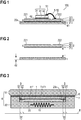
Figure 1 is a cross-sectional side view of an electronic assembly that includes a composite with a ceramic substrate bonded to a carrier. -
Figure 2 is a cross-sectional side view of the ceramic substrate, the carrier and a powder-including layer disposed in-between. -
Figure 3 is a cross-sectional side view of the ceramic substrate, the powder-including layer and the carrier stacked one upon the other and inserted in a pressing tool. -
Figure 4 is a top view of the arrangement ofFigure 3 . -
Figure 5 is a cross-sectional side view of the arrangement ofFigure 3 during sintering of the powder-including layer. -
Figure 6 shows timing diagrams of the temperature and pressure employed in the sintering process. -
Figure 7 is a cross-sectional side view of an arrangement that differs from the arrangement ofFigure 5 in that thecarrier 1 has cooling fins. - In the following detailed description, reference is made to the accompanying drawings. The drawings show specific examples in which the invention may be practiced. It is to be understood that the features and principles described with respect to the various examples may be combined with each other, unless specifically noted otherwise. As well as in the claims, designations of certain elements as "first element", "second element", "third element" etc. are not to be understood as enumerative. Instead, such designations serve solely to address different "elements". That is, e.g., the existence of a "third element" does not require the existence of a "first element" and a "second element".
- Referring to
Figure 1 , an exemplaryelectronic assembly 100 includes a composite with acarrier 1, aceramic substrate 2, and a first joininglayer 41 joining thecarrier 1 and theceramic substrate 2. Theceramic substrate 2 includes a dielectricceramic layer 20, an optional firstsubstrate metallization layer 21 and an optional secondsubstrate metallization layer 22. The firstsubstrate metallization layer 21 and the secondsubstrate metallization layer 22 are attached to opposite surfaces of theceramic layer 20. As illustrated, the secondsubstrate metallization layer 22 may be patterned to include at least twoconductor tracks - The dielectric
ceramic layer 20 may be made of any dielectric ceramic material, e.g. alumina (Al2O3), aluminum nitride (AlN) or silicon nitride (Si3N4), so that it can provide for an electrical insulation between the firstsubstrate metallization layer 21 and the secondsubstrate metallization layer 22, or at least for an electrical insulation between a conductor track formed in the firstsubstrate metallization layer 21 and a further conductor track formed in the secondsubstrate metallization layer 22. If it is desired that theceramic layer 20 electrically insulates the firstsubstrate metallization layer 21 from the secondsubstrate metallization layer 22, it may be free of electrically conductive vias. Alternatively, however, theceramic layer 20 of aceramic substrate 2 may include one or more electrically conductive vias electrically connecting the firstsubstrate metallization layer 21 and the secondsubstrate metallization layer 22. - The first
substrate metallization layer 21 and the secondsubstrate metallization layer 22 may include any metal, e.g. copper or aluminum, or metal alloy and be attached to opposite surfaces of theceramic layer 20 using any joining technique, e.g. brazing, direct copper bonding (DCB) or direct aluminum bonding (DAB). Optionally, at its side facing away from theceramic layer 20, the firstsubstrate metallization layer 21 may include a thin coating, for example in order to improve the sinterability. Irrespective of whether the first substrate metallization layer includes a coating or not, the secondsubstrate metallization layer 22 may, at its side facing away from theceramic layer 20, include a thin coating, for example in order to improve the solderability or the sinterability, or to protect the secondsubstrate metallization layer 22 against oxidation. A suitable coating for improving the solderability is, e.g., a layer consisting of or including Ni, and a suitable coating for improving the sinterability is, e.g., a layer consisting of or including a noble metal, e.g., Ag or Au or Pd. - The
carrier 1 serves to mechanically stabilize theceramic substrate 2. In order to provide for a proper stabilization, thecarrier 1 may have, without being restricted to, a thickness d2 of at least 2 mm. Thecarrier 1 may consist of or include metal. For instance, thesubstrate 1 may include at least 95 weight% copper or at least 95 weight% aluminum, or it may consist of or include a metal-matrix-composite (MMC) material like aluminum silicon carbide or any other MMC-material. - The first joining
layer 41 adjoins both thecarrier 1 and theceramic substrate 2 and causes a substance-to-substance bond between thecarrier 1 and theceramic substrate 2. As will be explained in more detail below, the first joininglayer 41 is formed by sintering a powder during a sintering process which includes a pressing and temperature process. - Disposed on that side of the second
substrate metallization layer 22 facing away from theceramic layer 20 is anelectronic component 3, e.g. a power semiconductor chip. An example of anelectronic component 3 formed as a power semiconductor chip is illustrated inFigure 1 . The power semiconductor chip includes asemiconductor body 30, a firstchip metallization layer 31 and a secondchip metallization layer 32. A second joininglayer 42 creating a substance-to-substance bond between theceramic substrate 2 and theelectronic component 3 adjoins both the ceramic substrate 2 (e.g. that surface of thesecond metallization layer 22 facing away from the ceramic layer 20) and the electronic component 3 (here: that surface of the secondchip metallization layer 32 facing away from the semiconductor body 30). The second joininglayer 42 may be a solder layer, a layer including a sintered metal powder, or a layer of an electrically conductive or electrically insulating adhesive. - Using the
ceramic substrate 2 as a circuit board forms basis the realization of any desired electronic circuit. That is, an arbitrary number of electronic components may be disposed on theceramic substrate 2 and electrically interconnected using any type ofinterconnects 5, e.g. bonding wires (as shown), metal sheets (not shown), etc. In the example illustrated inFigure 1 , abonding wire 5 is, at afirst bonding location 51, wire bonded to the firstchip metallization layer 31, and, at asecond bonding location 52, to the secondsubstrate metallization layer 22. According to the illustrated example, thesemiconductor chip 3 may be mounted on afirst conductor track 221 formed in the second substrate metallization layer 22 (so that the second joininglayer 42 adjoins thefirst conductor track 221 and joins thesemiconductor chip 3 to theceramic substrate 2 at the first conductor track 221). Thefirst bonding location 51 may be a location at the firstchip metallization layer 31, and thesecond bonding location 52 may be a location at asecond conductor track 222 formed in the secondsubstrate metallization layer 22. -
Figure 2 illustrates thecarrier 1 and theceramic substrate 2 prior to being joined. In order to join thecarrier 1 and theceramic substrate 2, a powder-including layer 41' may be applied to that surface of the firstsubstrate metallization layer 21 facing away from theceramic layer 20, and/or a powder-including layer 41' may be applied to thecarrier 1. The powder included in the powder-including layer(s) 41' may be a metal powder, e.g. a silver powder. The powder-including layer(s) 41' may be applied to the firstsubstrate metallization layer 21 or thecarrier 1, respectively, in the form of a paste including the metal powder and a solvent. After applying the powder-including layer(s) 41', it may be dried by evaporating most of the solvent so that metal powder remains on the firstsubstrate metallization layer 21 or thecarrier 1. If there is only one powder-including layer(s) 41', the paste may be applied to either the firstsubstrate metallization layer 21 or thecarrier 1 and be subsequently dried. Then, the dried layer 41' may be disposed between thecarrier 1 and thesubstrate metallization layer 21 so that that the dried layer 41' forms a powder-includinglayer 41" (Figure 3 ) that adjoins both thecarrier 1 and thesubstrate metallization layer 21. - If there are two powder-including layers 41', the paste may be applied to both the first
substrate metallization layer 21 or thecarrier 1 and be subsequently dried so that one dried powder-including layer 41' adheres to thecarrier 1 and a further dried powder-including layer 41' adheres to the firstsubstrate metallization layer 21. Subsequently, the dried powder-including layers 41' may be disposed between thecarrier 1 and thesubstrate metallization layer 21 so that that they unify to a powder-includinglayer 41" (Figure 3 ) that adjoins both thecarrier 1 and thesubstrate metallization layer 21. - Subsequently, the metal powder included in the powder-including
layer 41" will be sintered during a sintering process so as to form from it the first joininglayer 41 described above with reference toFigure 1 . As illustrated inFigure 3 , sintering takes place using apressing tool 6. Thepressing tool 6 includes a firstpressing tool element 61 and a secondpressing tool element 62. The stack including thecarrier 1, theceramic substrate 2 and the powder-includinglayer 41" disposed in-between is placed between the firstpressing tool element 61 and the secondpressing tool element 62, and, subsequently, thecarrier 1 and theceramic substrate 2 with the powder-includinglayer 41" disposed in-between are pressed against one another by pressing thefirst pressure piece 61 and thesecond pressure piece 62 towards one another.. - Optionally, a foil layer which includes at least one
foil pressing tool element 61 on the one hand and the stack with thecarrier 1, theceramic substrate 2 and the powder-includinglayer 41" disposed in-between on the other. According to one option, the foil layer may include anon-stick foil 8, e.g. made of polytetrafluoroethylene, which makes sure that the firstpressing tool element 61 can, after the pressing process, be removed from the secondpressing tool element 62, from the composite including thecarrier 1, theceramic substrate 2 and the first joininglayer 41 disposed in-between, and, if present, from one or more further foils (here: a metal foil 7) of the foil layer disposed between thenon-stick foil 8 and the mentioned composite. A suitable thickness of the non-stick 8 may be, without being restricted to, 100 µm. - According to another option, the foil layer may include a metal foil 7 (e.g. made of hardened steel) that is disposed between the first
pressing tool element 61 on the one hand and the stack with thecarrier 1, theceramic substrate 2 and the powder-includinglayer 41" disposed in-between on the other. Themetal foil 7 serves to protect in particular the substrate from being damaged during the pressing process, e.g. when the firstpressing tool element 61 is a flexible pressure pillow that allows for applying an approximately hydrostatic (i.e. evenly distributed) pressure to one side of the mentioned stack. Depending on the dimensions of thepressing tool 6, the flexibility of the firstpressing tool element 61 formed as a pressure pillow, and the orientation of the stack inserted in thepressing tool 6, a firstpressing tool element 61 formed as a pressure pillow might partly be pressed into a gap between the secondpressing tool element 62 and the mentioned stack and cause a crack of thesubstrate 2, in particular of theceramic layer 20. If the gap between the secondpressing tool element 62 and the mentioned stack is not too wide, themetal foil 7 can prevent the firstpressing tool element 61 formed as a flexible pressure pillow from being pressed into the gap. A suitable thickness of themetal foil 7 is, without being restricted to, 100 µm. - The
second tool element 62 is made of a hard material. For instance, thesecond tool element 62 may have, without being restricted to, a rockwell hardness of at least 29. A suitable material having a rockwell hardness of at least 29 is, for instance, AMPCO® 21 (an alloy including at least 80,0 weight% Cu; 13.1 weight% Al; 4.4 weight% Fe; 2.0 weight% Mn; other: less than or equal to 0.5 weight%). - An alternative or additional means for preventing the formation of a crack of the
substrate 2 during the pressing process is the use of acarrier 1 that laterally extends at least as far as or even beyond thesubstrate 2 so that it "shields" thesubstrate 2 from damaging impacts caused by a firstpressing tool element 61 formed as a flexible pressure pillow. In this regard, "laterally" designates a direction parallel to a surface of theceramic layer 20 facing toward thecarrier 1. In order to produce that shielding effect, thecarrier 1 is disposed between thesubstrate 2 and the firstpressing tool element 1. InFigure 3 , reference numeral '12' designates the lateral overhang thecarrier 1 has relative to theceramic substrate 2. Thelateral overhang 12 may be determined from an orthogonal projection of thecarrier 1 and thesubstrate 2 of the mentioned stack onto a projection plane E. A top view of the projection plane E ofFigure 3 is illustrated inFigure 4 . InFigure 4 , the outline of the projection of thecarrier 1 into the projection plane E has is indicated by a dot and dash line, and the outline the projection of thesubstrate 2 into the projection plane E has is indicated by a dotted line. The projection plane E may run parallel to a surface orsurface section 20s of theceramic layer 20 facing toward thecarrier 1. If thesubstrate 2 has a substantially flat shape, the orientation of the projection plane E is substantially parallel to thesubstrate 2. The direction of the projection runs perpendicular to the projection plane E. As can be seen fromFigure 4 , alateral overhang 12 can be achieved when thecarrier 1 has a (maximum) footprint area A1 greater than a (maximum) footprint area A2 of theceramic substrate 2. - According to another option, the
lateral overhang 12 in the projection plane E may everywhere be greater than zero so that the outline of the projection of thesubstrate 2 into the projection plane E is fully inside but distant from the outline of the projection of thecarrier 1 into the projection plane E (that is, thelateral overhang 12 is a closed ring that everywhere has a width greater than zero). - At locations where the
carrier 1 has alateral overhang 12 greater than zero, aspacer 9 may, adjacent to thesubstrate 2, be disposed between the secondpressing tool element 62 and the carrier 1 (in the region of the lateral overhang 12) in order to support thecarrier 1 when the latter is pressed by the firstpressing tool element 61 towards the secondpressing tool element 62. Thespacer 9 can prevent thecarrier 1 from being bent by the firstpressing tool element 61. During the pressing process, the powder-includinglayer 41" is compressed and its thickness is reduced. Therefore, the height of such a spacer 9 (if used) may be adjusted to the sum of the thickness of thesubstrate 2 and the desired thickness of the completed first joininglayer 41 to be produced by the sintering process. Thespacer 9 includes at least onedistance piece 91 and, optionally, at least oneadjustment piece 92 stacked on thedistance piece 91 so that the total height of thespacer 9 is equal to the sum of the thickness of thesubstrate 2 and the desired thickness of the first joininglayer 41 to be produced. For instance, thedistance piece 91, and, as far as provided, eachadjustment piece 92 may be a ring surrounding thesubstrate 2. - In order to form the first joining layer 41 (
Figure 1 ) from the powder-includinglayer 41" (Figure 3 ), the powder included in the powder-includinglayer 41" is sintered during a sintering process in which the powder-includinglayer 41" is compressed and heated to temperatures significantly higher than room temperature. Heating the powder-includinglayer 41" to high temperatures also causes thecarrier 1 and thesubstrate 2 to heat up and, as a consequence, to expand depending on their respective coefficient of thermal expansion. The coefficient of thermal expansion (CTE) of thesubstrate 2 is significantly determined by the coefficient of thermal expansion of theceramic layer 20 and the coefficient(s) of thermal expansion of the first and second substrate metallization layers 21, 22. If the CTE of thecarrier 1 exceeds the CTE of thesubstrate 2, heating thecarrier 1, theceramic substrate 2 and the powder-includinglayer 41" disposed in-between in a state in which thecarrier 1, theceramic substrate 2 and the powder-includinglayer 41" are pressed against one another at a high pressure, to high temperatures will cause a tensile load on thesubstrate 2 and, thus, on theceramic layer 20. Because the strength of ceramics against tensile loads is poor, there is a significant risk of a crack occurring in theceramic layer 20 during the sintering process. - In order to prevent such cracks, the
carrier 1 is pre-heated, and a high pressure with which thecarrier 1, theceramic substrate 2 and the powder-includinglayer 41" disposed in-between are pressed against one another in order to sinter the powder-includinglayer 41 ", is applied when thecarrier 1 has already reached the pre-heated state. Applying the high pressure may substantially be caused by pressing thepre-heated carrier 1 and theceramic substrate 2 with the powder-includinglayer 41" disposed in-between against one another by pressing thefirst pressure piece 61 and thesecond pressure piece 62 towards one another. - By sintering the powder-including
layer 41", the powder-includinglayer 41" is converted into the first joining layer 41 (Figure 1 ) and causes a firm substance-to-substance bond between thecarrier 1 and theceramic substrate 2. Because the CTE of thecarrier 1 exceeds the CTE of thesubstrate 2, subsequently cooling down the achieved assembly which includes thecarrier 1, theceramic substrate 2 and the first joininglayer 41 joining thecarrier 1 and theceramic substrate 2 to, e.g., room temperature (20°C), a compressive load on thesubstrate 2 and, thus, on theceramic layer 20 is caused. Because the compressive strength of ceramics is significantly higher than its tensile strength, the pre-heating helps prevent the formation of cracks in theceramic layer 20. - Referring to the
Figure 6 , the steps of pre-heating and sintering outlined above will be described in more detail below. Thereby, "T" designates a temperature of thecarrier 1, and "p" designates a pressure (if any) with which thecarrier 1, theceramic substrate 2 and the powder-includinglayer 41" disposed in-between are pressed against one another. The upper diagram illustrates the temperature T depending on the time t, and the upper diagram illustrates the temperature T depending on the time t, and the upper diagram illustrates the pressure depending on the time t. The time scales of both diagrams are identical. - In order to pre-heat the
carrier 1, the temperature T is increased from an initial temperature T0 to at least a first temperature threshold T1 (see alsoFigure 3 ). In the following, designating thecarrier 1 as "pre-heated" means that the temperature T is at least T1. At a first point of time t1, the temperature T has reached T1. - Subsequent to reaching the first temperature T1, i.e. subsequent to the first point of time t1, the
ceramic substrate 2 and thepre-heated carrier 1 with the powder-includinglayer 41" disposed in-between are pressed against one another with a pressure p of at least a first pressure threshold p1 (see alsoFigure 5 ). That is, in a state, in which the temperature T is permanently at least the first threshold temperature T1, the pressure p is increased from less than or equal to an initial pressure threshold p0 to at least the first pressure threshold p1. InFigure 6 , a second point of time t2 designates the point of time at which the increasing pressure p reaches the first pressure threshold p1. - The initial pressure threshold p0 is sufficiently low to allow for a certain relative movement between the
carrier 1 and thesubstrate 2 so that, when the temperature T is increased from T0 to at least the first threshold temperature T1, no substantial tensile load affects theceramic layer 20. A suitable value for the initial pressure threshold p0 is, without being restricted to, 8.5E-04 MPa (megapascal). The low pressure threshold p0 may substantially be caused by the self-weight of the elements of the stack with thesubstrate 2, the powder-includinglayer 41" and thecarrier 1, and, as far as provided, by the self-weights of the foil layer and the firstpressing tool element 61. - The first pressure threshold p1 and the first temperature threshold T1 are sufficiently high to allow for fast and reliably producing the first joining
layer 41 from the powder-includinglayer 41" by sintering. A suitable value for the first pressure threshold p1 is, without being restricted to, at least 20 MPa or even at least 30 MPa. A suitable value for the first temperature threshold T1 is, without being restricted to, a temperature which allows for sintering the powder-including layer when it is heated to that temperature. For instance, the first temperature threshold T1 may be at least 200°C or even at least 300°C. - After simultaneously keeping the pressure p at at least the first pressure threshold p1 and the temperature T at at least the first temperature threshold T1 for at least a minimum sintering time Δt, the powder-including
layer 41" is sintered and thereby converted into the first joininglayer 41 which forms a stable sintered joint between thecarrier 1 and thesubstrate 2. InFigure 6 , a third point of time t3 designates the point of time at which the minimum sintering time Δt lapses. That is, the minimum sintering time Δt is the time difference between the third point of time t3 and the second point of time t2. - Subsequent to the minimum sintering time Δt, the temperature T may be decreased to below the first temperature threshold T1 (e.g. to the initial temperature T0) and the pressure p may be decreased to below the first pressure threshold p1 (e.g. to below the initial pressure threshold p0). A suitable value for the minimum sintering time Δt is, without being restricted to, at least 30 s (seconds), or even at least 120 s.
- In order to prevent damage to the
ceramic layer 20 due to excessive pressure, the pressure p may be kept below 50 MPa during the whole process, in particular during the minimum sintering time Δt. Optionally, the initial pressure p0 may be zero which can be achieved by pre-heating thecarrier 1 in a state in which thecarrier 1 is not yet placed on thesubstrate 2 and by subsequently placing thepre-heated carrier 1 on thesubstrate 2 with the powder-includinglayer 41" disposed in-between so that the powder-includinglayer 41" adjoins both thepre-heated carrier 1 and thesubstrate 2. Also optionally, the whole sintering process (i.e. the sintering of the powder-includinglayer 41 ") may be a dry sintering process so that no liquid phases occur within the powder-includinglayer 41". During the sintering process, thecarrier 1 and thesubstrate 2 are not melted. - For heating the
carrier 1 to the mentioned temperatures T, any suitable heating may be used. InFigures 3 and5 , theheating 10 is shown only schematically. For instance, theheating 10 may be integrated in the second pressing tool element 62 (e.g. as an electrical heating resistor). Theheating 10 may also be external to the secondpressing tool element 62. For example, theheating 10 may be a hot plate that is brought into contact with and heats the secondpressing tool element 62. It is also possible that theheating 10 is an inductive heating. - Irrespective of the type of
heating 10, heating thecarrier 1 may include indirectly heating thecarrier 1 by heat that disperses from the secondpressing tool element 62 via the first pressing tool element 61 (and, if provided, thefoil layer 7, 8) and via thesubstrate 2 and the powder-includinglayer 41". - If the first
pressing tool element 61 is a flexible pressure pillow, the grade of flexibility may be adjusted by its shore-A-hardness. The pressure caused by a firstpressing tool element 61 formed as a flexible pressure pillow is as closer to a hydrostatic pressure the lower the shore-A-hardness of the pressure pillow is. For a firstpressing tool element 61 formed as a flexible pressure pillow, a suitable shore-A-hardness may be less than or equal to 90, e.g. in a range from 10 to 90 (at a temperature of the pressure pillow of 20°C in every case). However, it is to be noted that instead of a flexible pressure pillow, a rigid firstpressing tool element 61, for example made of metal (e.g. steel), may also be used. - When the sintering process is completed, i.e. subsequent to the minimum sintering time Δt, the composite which includes the
carrier 1, theceramic substrate 2 and the first joininglayer 41 may be removed from thepressing tool 6 and, if provided, thespacer 9. In order to achieve anelectronic assembly 100 described with reference toFigure 1 , one or moreelectronic components 3, e.g. semiconductor chips, may be mounted on theceramic substrate 2 using a second joininglayer 42, and electrically interconnected usinginterconnects 5, e.g. one or more bonding wires. -
Figure 7 shows an arrangement according toFigure 5 . The only difference to the arrangement ofFigure 5 is that thecarrier 1 has a plurality of coolingfins 11. As illustrated, the coolingfins 11 may, at least during the minimum sintering time Δt, be disposed at that side of thecarrier 1 facing away from thesubstrate 2. - Spatially relative terms such as "under", "below", "lower", "over", "upper" and the like, are used for ease of description to explain the positioning of one element relative to a second element. These terms are intended to encompass different orientations of the device in addition to different orientations than those depicted in the figures. Further, terms such as "first", "second", and the like, are also used to describe various elements, regions, sections, etc. and are also not intended to be limiting. Like terms refer to like elements throughout the description.
Claims (15)
- A method for producing a sintered joint between a ceramic substrate and a carrier, the method comprising:pre-heating the carrier by increasing a temperature of the carrier from an initial temperature to at least a first threshold temperature;increasing a pressure, with which the pre-heated carrier, the ceramic substrate and a powder-including layer disposed between the pre-heated carrier and the ceramic substrate are pressed against one another, from an initial pressure of less than or equal to an initial pressure threshold to at least a first pressure threshold;sintering the powder-including layer by simultaneously keeping the pressure for at least a minimum sintering time at at least the first pressure threshold and the temperature of the carrier at at least the first temperature threshold so that the powder-including layer is converted into a joining layer joining the carrier and the ceramic substrate; whereinthe first temperature threshold is a temperature which allows for sintering the powder-including layer when it is heated to that temperature.
- The method of claim 1, wherein pressing the pre-heated carrier and the ceramic substrate with the powder-including layer disposed in-between against one another comprises
disposing a stack which comprises the carrier, the ceramic substrate and the powder-including layer disposed between the carrier and the ceramic substrate between a first pressure piece formed as a flexible pressure pillow and a second pressure piece so that the carrier is disposed between the first pressure piece and the ceramic substrate and has a maximum footprint area greater than a maximum footprint area of the ceramic substrate; and
pressing the pre-heated carrier, the ceramic substrate and the powder-including layer disposed between the pre-heated carrier and the ceramic substrate against one another by pressing the first pressure piece and the second pressure piece towards one another. - The method of claim 2, wherein the carrier has, when the pre-heated carrier, the ceramic substrate and the powder-including layer disposed between the pre-heated carrier and the ceramic substrate are pressed against one another, relative to the substrate, a lateral overhang that is formed as a closed ring.
- The method of claim 2 or 3, wherein, adjacent to the substrate, a spacer is disposed between the carrier and the second pressure piece.
- The method of any of the preceding claims, wherein
the ceramic substrate comprises a ceramic layer, a first substrate metallization layer attached to the ceramic layer and a second substrate metallization layer attached to the ceramic layer; and
the ceramic layer is disposed between the first substrate metallization layer and the second substrate metallization layer. - The method of any of the preceding claims, wherein the first pressure threshold is at least 20 MPa or at least 30 MPa.
- The method of any of the preceding claims, wherein the pressure is, at least for the minimum sintering time, below 50 MPa.
- The method of any of the preceding claims, wherein the minimum sintering time is at least 30 s or at least 120 s.
- The method of any of the preceding claims, wherein the first temperature threshold is at least 200°C.
- The method of any of the preceding claims, wherein the first temperature threshold is at least 300°C.
- The method of any of the preceding claims, wherein, after the minimum sintering time,
the temperature is decreased to below the first temperature threshold; and
the pressure is decreased to below the first pressure threshold. - The method of any of the preceding claims, wherein the carrier consists of or comprises metal.
- The method of any of the preceding claims, wherein the carrier comprises a plurality of cooling fins which are, at least during the minimum sintering time, disposed at that side of the carrier facing away from the ceramic substrate.
- The method of any of the preceding claims, wherein the powder-including layer consists of or comprises a metal powder.
- The method of claim 14, wherein the metal powder is a silver powder.
Priority Applications (1)
| Application Number | Priority Date | Filing Date | Title |
|---|---|---|---|
| EP17168793.2A EP3395783B1 (en) | 2017-04-28 | 2017-04-28 | Method for producing a sintered joint between a ceramic substrate and a carrier |
Applications Claiming Priority (1)
| Application Number | Priority Date | Filing Date | Title |
|---|---|---|---|
| EP17168793.2A EP3395783B1 (en) | 2017-04-28 | 2017-04-28 | Method for producing a sintered joint between a ceramic substrate and a carrier |
Publications (2)
| Publication Number | Publication Date |
|---|---|
| EP3395783A1 true EP3395783A1 (en) | 2018-10-31 |
| EP3395783B1 EP3395783B1 (en) | 2019-09-25 |
Family
ID=58672376
Family Applications (1)
| Application Number | Title | Priority Date | Filing Date |
|---|---|---|---|
| EP17168793.2A Active EP3395783B1 (en) | 2017-04-28 | 2017-04-28 | Method for producing a sintered joint between a ceramic substrate and a carrier |
Country Status (1)
| Country | Link |
|---|---|
| EP (1) | EP3395783B1 (en) |
Citations (3)
| Publication number | Priority date | Publication date | Assignee | Title |
|---|---|---|---|---|
| US5486976A (en) * | 1994-11-14 | 1996-01-23 | Texas Instruments Incorporated | Pressure transducer apparatus having a rigid member extending between diaphragms |
| US20150028725A1 (en) * | 2011-07-18 | 2015-01-29 | Renault S.A.S. | Method of assembling an ultrasonic transducer and the transducer obtained thereby |
| US20160148819A1 (en) * | 2014-11-20 | 2016-05-26 | Infineon Technologies Ag | Method for Producing a Material-Bonding Connection between a Semiconductor Chip and a Metal Layer |
-
2017
- 2017-04-28 EP EP17168793.2A patent/EP3395783B1/en active Active
Patent Citations (3)
| Publication number | Priority date | Publication date | Assignee | Title |
|---|---|---|---|---|
| US5486976A (en) * | 1994-11-14 | 1996-01-23 | Texas Instruments Incorporated | Pressure transducer apparatus having a rigid member extending between diaphragms |
| US20150028725A1 (en) * | 2011-07-18 | 2015-01-29 | Renault S.A.S. | Method of assembling an ultrasonic transducer and the transducer obtained thereby |
| US20160148819A1 (en) * | 2014-11-20 | 2016-05-26 | Infineon Technologies Ag | Method for Producing a Material-Bonding Connection between a Semiconductor Chip and a Metal Layer |
Also Published As
| Publication number | Publication date |
|---|---|
| EP3395783B1 (en) | 2019-09-25 |
Similar Documents
| Publication | Publication Date | Title |
|---|---|---|
| KR102094566B1 (en) | Power module substrate and power module | |
| JP5786569B2 (en) | Power module substrate manufacturing method | |
| KR102154369B1 (en) | Power module | |
| US12021043B2 (en) | Semiconductor device and method for manufacturing semiconductor device | |
| US8050054B2 (en) | Electronic device with a base plate | |
| JP7024331B2 (en) | A method for manufacturing an insulated circuit board, a method for manufacturing an insulated circuit board with a heat sink, and a method for manufacturing a laminated structure of an insulated circuit board. | |
| US10600658B2 (en) | Apparatus and method for bending a substrate | |
| JP2013118299A (en) | Substrate for power module | |
| JP2018110149A (en) | Manufacturing method of semiconductor device | |
| JP2013229564A (en) | Manufacturing method of substrate for power module | |
| KR20200134206A (en) | Insulated circuit board and method of manufacturing insulated circuit board | |
| JP7342371B2 (en) | Insulated circuit board and method for manufacturing an insulated circuit board | |
| JP5987418B2 (en) | Manufacturing method of power module substrate with heat sink | |
| EP3761764A1 (en) | Insulating circuit board | |
| JP6790945B2 (en) | Manufacturing method of insulated circuit board and manufacturing method of insulated circuit board with heat sink | |
| EP3395783B1 (en) | Method for producing a sintered joint between a ceramic substrate and a carrier | |
| JP2015095624A (en) | Bonded body and power module substrate | |
| EP3547352B1 (en) | Method for joining two joining members | |
| JP3934966B2 (en) | Ceramic circuit board | |
| JP7039933B2 (en) | Bond, Insulated Circuit Board, Insulated Circuit Board with Heat Sink, Heat Sink, and Joined Body Manufacturing Method, Insulated Circuit Board Manufacturing Method, Heat Sinked Insulated Circuit Board Manufacturing Method, Heat Sink Manufacturing Method | |
| CN117080171A (en) | Power semiconductor module device and manufacturing method thereof | |
| EP3457434B1 (en) | Method for producing a semiconductor substrate for a power semiconductor module arrangement | |
| CN115669242A (en) | Manufacturing method of insulating resin circuit board | |
| CN117897366B (en) | Copper-ceramic joined body and insulating circuit board | |
| JP2002076213A (en) | Semiconductor element module |
Legal Events
| Date | Code | Title | Description |
|---|---|---|---|
| PUAI | Public reference made under article 153(3) epc to a published international application that has entered the european phase |
Free format text: ORIGINAL CODE: 0009012 |
|
| STAA | Information on the status of an ep patent application or granted ep patent |
Free format text: STATUS: THE APPLICATION HAS BEEN PUBLISHED |
|
| AK | Designated contracting states |
Kind code of ref document: A1 Designated state(s): AL AT BE BG CH CY CZ DE DK EE ES FI FR GB GR HR HU IE IS IT LI LT LU LV MC MK MT NL NO PL PT RO RS SE SI SK SM TR |
|
| AX | Request for extension of the european patent |
Extension state: BA ME |
|
| STAA | Information on the status of an ep patent application or granted ep patent |
Free format text: STATUS: REQUEST FOR EXAMINATION WAS MADE |
|
| 17P | Request for examination filed |
Effective date: 20190207 |
|
| RBV | Designated contracting states (corrected) |
Designated state(s): AL AT BE BG CH CY CZ DE DK EE ES FI FR GB GR HR HU IE IS IT LI LT LU LV MC MK MT NL NO PL PT RO RS SE SI SK SM TR |
|
| GRAP | Despatch of communication of intention to grant a patent |
Free format text: ORIGINAL CODE: EPIDOSNIGR1 |
|
| STAA | Information on the status of an ep patent application or granted ep patent |
Free format text: STATUS: GRANT OF PATENT IS INTENDED |
|
| RIC1 | Information provided on ipc code assigned before grant |
Ipc: C04B 37/02 20060101ALI20190311BHEP Ipc: C04B 35/626 20060101AFI20190311BHEP Ipc: H01L 23/00 20060101ALI20190311BHEP |
|
| INTG | Intention to grant announced |
Effective date: 20190405 |
|
| GRAS | Grant fee paid |
Free format text: ORIGINAL CODE: EPIDOSNIGR3 |
|
| GRAA | (expected) grant |
Free format text: ORIGINAL CODE: 0009210 |
|
| STAA | Information on the status of an ep patent application or granted ep patent |
Free format text: STATUS: THE PATENT HAS BEEN GRANTED |
|
| AK | Designated contracting states |
Kind code of ref document: B1 Designated state(s): AL AT BE BG CH CY CZ DE DK EE ES FI FR GB GR HR HU IE IS IT LI LT LU LV MC MK MT NL NO PL PT RO RS SE SI SK SM TR |
|
| REG | Reference to a national code |
Ref country code: GB Ref legal event code: FG4D |
|
| REG | Reference to a national code |
Ref country code: CH Ref legal event code: EP |
|
| REG | Reference to a national code |
Ref country code: AT Ref legal event code: REF Ref document number: 1183683 Country of ref document: AT Kind code of ref document: T Effective date: 20191015 |
|
| REG | Reference to a national code |
Ref country code: IE Ref legal event code: FG4D |
|
| REG | Reference to a national code |
Ref country code: DE Ref legal event code: R096 Ref document number: 602017007242 Country of ref document: DE |
|
| REG | Reference to a national code |
Ref country code: NL Ref legal event code: MP Effective date: 20190925 |
|
| PG25 | Lapsed in a contracting state [announced via postgrant information from national office to epo] |
Ref country code: FI Free format text: LAPSE BECAUSE OF FAILURE TO SUBMIT A TRANSLATION OF THE DESCRIPTION OR TO PAY THE FEE WITHIN THE PRESCRIBED TIME-LIMIT Effective date: 20190925 Ref country code: SE Free format text: LAPSE BECAUSE OF FAILURE TO SUBMIT A TRANSLATION OF THE DESCRIPTION OR TO PAY THE FEE WITHIN THE PRESCRIBED TIME-LIMIT Effective date: 20190925 Ref country code: HR Free format text: LAPSE BECAUSE OF FAILURE TO SUBMIT A TRANSLATION OF THE DESCRIPTION OR TO PAY THE FEE WITHIN THE PRESCRIBED TIME-LIMIT Effective date: 20190925 Ref country code: LT Free format text: LAPSE BECAUSE OF FAILURE TO SUBMIT A TRANSLATION OF THE DESCRIPTION OR TO PAY THE FEE WITHIN THE PRESCRIBED TIME-LIMIT Effective date: 20190925 Ref country code: NO Free format text: LAPSE BECAUSE OF FAILURE TO SUBMIT A TRANSLATION OF THE DESCRIPTION OR TO PAY THE FEE WITHIN THE PRESCRIBED TIME-LIMIT Effective date: 20191225 Ref country code: BG Free format text: LAPSE BECAUSE OF FAILURE TO SUBMIT A TRANSLATION OF THE DESCRIPTION OR TO PAY THE FEE WITHIN THE PRESCRIBED TIME-LIMIT Effective date: 20191225 |
|
| REG | Reference to a national code |
Ref country code: LT Ref legal event code: MG4D |
|
| PG25 | Lapsed in a contracting state [announced via postgrant information from national office to epo] |
Ref country code: LV Free format text: LAPSE BECAUSE OF FAILURE TO SUBMIT A TRANSLATION OF THE DESCRIPTION OR TO PAY THE FEE WITHIN THE PRESCRIBED TIME-LIMIT Effective date: 20190925 Ref country code: RS Free format text: LAPSE BECAUSE OF FAILURE TO SUBMIT A TRANSLATION OF THE DESCRIPTION OR TO PAY THE FEE WITHIN THE PRESCRIBED TIME-LIMIT Effective date: 20190925 Ref country code: GR Free format text: LAPSE BECAUSE OF FAILURE TO SUBMIT A TRANSLATION OF THE DESCRIPTION OR TO PAY THE FEE WITHIN THE PRESCRIBED TIME-LIMIT Effective date: 20191226 |
|
| REG | Reference to a national code |
Ref country code: AT Ref legal event code: MK05 Ref document number: 1183683 Country of ref document: AT Kind code of ref document: T Effective date: 20190925 |
|
| PG25 | Lapsed in a contracting state [announced via postgrant information from national office to epo] |
Ref country code: IT Free format text: LAPSE BECAUSE OF FAILURE TO SUBMIT A TRANSLATION OF THE DESCRIPTION OR TO PAY THE FEE WITHIN THE PRESCRIBED TIME-LIMIT Effective date: 20190925 Ref country code: RO Free format text: LAPSE BECAUSE OF FAILURE TO SUBMIT A TRANSLATION OF THE DESCRIPTION OR TO PAY THE FEE WITHIN THE PRESCRIBED TIME-LIMIT Effective date: 20190925 Ref country code: PL Free format text: LAPSE BECAUSE OF FAILURE TO SUBMIT A TRANSLATION OF THE DESCRIPTION OR TO PAY THE FEE WITHIN THE PRESCRIBED TIME-LIMIT Effective date: 20190925 Ref country code: PT Free format text: LAPSE BECAUSE OF FAILURE TO SUBMIT A TRANSLATION OF THE DESCRIPTION OR TO PAY THE FEE WITHIN THE PRESCRIBED TIME-LIMIT Effective date: 20200127 Ref country code: NL Free format text: LAPSE BECAUSE OF FAILURE TO SUBMIT A TRANSLATION OF THE DESCRIPTION OR TO PAY THE FEE WITHIN THE PRESCRIBED TIME-LIMIT Effective date: 20190925 Ref country code: ES Free format text: LAPSE BECAUSE OF FAILURE TO SUBMIT A TRANSLATION OF THE DESCRIPTION OR TO PAY THE FEE WITHIN THE PRESCRIBED TIME-LIMIT Effective date: 20190925 Ref country code: AL Free format text: LAPSE BECAUSE OF FAILURE TO SUBMIT A TRANSLATION OF THE DESCRIPTION OR TO PAY THE FEE WITHIN THE PRESCRIBED TIME-LIMIT Effective date: 20190925 Ref country code: AT Free format text: LAPSE BECAUSE OF FAILURE TO SUBMIT A TRANSLATION OF THE DESCRIPTION OR TO PAY THE FEE WITHIN THE PRESCRIBED TIME-LIMIT Effective date: 20190925 Ref country code: EE Free format text: LAPSE BECAUSE OF FAILURE TO SUBMIT A TRANSLATION OF THE DESCRIPTION OR TO PAY THE FEE WITHIN THE PRESCRIBED TIME-LIMIT Effective date: 20190925 |
|
| PG25 | Lapsed in a contracting state [announced via postgrant information from national office to epo] |
Ref country code: CZ Free format text: LAPSE BECAUSE OF FAILURE TO SUBMIT A TRANSLATION OF THE DESCRIPTION OR TO PAY THE FEE WITHIN THE PRESCRIBED TIME-LIMIT Effective date: 20190925 Ref country code: SK Free format text: LAPSE BECAUSE OF FAILURE TO SUBMIT A TRANSLATION OF THE DESCRIPTION OR TO PAY THE FEE WITHIN THE PRESCRIBED TIME-LIMIT Effective date: 20190925 Ref country code: SM Free format text: LAPSE BECAUSE OF FAILURE TO SUBMIT A TRANSLATION OF THE DESCRIPTION OR TO PAY THE FEE WITHIN THE PRESCRIBED TIME-LIMIT Effective date: 20190925 Ref country code: IS Free format text: LAPSE BECAUSE OF FAILURE TO SUBMIT A TRANSLATION OF THE DESCRIPTION OR TO PAY THE FEE WITHIN THE PRESCRIBED TIME-LIMIT Effective date: 20200224 |
|
| REG | Reference to a national code |
Ref country code: DE Ref legal event code: R097 Ref document number: 602017007242 Country of ref document: DE |
|
| PG2D | Information on lapse in contracting state deleted |
Ref country code: IS |
|
| PG25 | Lapsed in a contracting state [announced via postgrant information from national office to epo] |
Ref country code: DK Free format text: LAPSE BECAUSE OF FAILURE TO SUBMIT A TRANSLATION OF THE DESCRIPTION OR TO PAY THE FEE WITHIN THE PRESCRIBED TIME-LIMIT Effective date: 20190925 Ref country code: IS Free format text: LAPSE BECAUSE OF FAILURE TO SUBMIT A TRANSLATION OF THE DESCRIPTION OR TO PAY THE FEE WITHIN THE PRESCRIBED TIME-LIMIT Effective date: 20200126 |
|
| PLBE | No opposition filed within time limit |
Free format text: ORIGINAL CODE: 0009261 |
|
| STAA | Information on the status of an ep patent application or granted ep patent |
Free format text: STATUS: NO OPPOSITION FILED WITHIN TIME LIMIT |
|
| 26N | No opposition filed |
Effective date: 20200626 |
|
| PG25 | Lapsed in a contracting state [announced via postgrant information from national office to epo] |
Ref country code: MC Free format text: LAPSE BECAUSE OF FAILURE TO SUBMIT A TRANSLATION OF THE DESCRIPTION OR TO PAY THE FEE WITHIN THE PRESCRIBED TIME-LIMIT Effective date: 20190925 Ref country code: SI Free format text: LAPSE BECAUSE OF FAILURE TO SUBMIT A TRANSLATION OF THE DESCRIPTION OR TO PAY THE FEE WITHIN THE PRESCRIBED TIME-LIMIT Effective date: 20190925 |
|
| REG | Reference to a national code |
Ref country code: CH Ref legal event code: PL |
|
| PG25 | Lapsed in a contracting state [announced via postgrant information from national office to epo] |
Ref country code: LU Free format text: LAPSE BECAUSE OF NON-PAYMENT OF DUE FEES Effective date: 20200428 Ref country code: CH Free format text: LAPSE BECAUSE OF NON-PAYMENT OF DUE FEES Effective date: 20200430 Ref country code: LI Free format text: LAPSE BECAUSE OF NON-PAYMENT OF DUE FEES Effective date: 20200430 Ref country code: FR Free format text: LAPSE BECAUSE OF NON-PAYMENT OF DUE FEES Effective date: 20200430 |
|
| REG | Reference to a national code |
Ref country code: BE Ref legal event code: MM Effective date: 20200430 |
|
| PG25 | Lapsed in a contracting state [announced via postgrant information from national office to epo] |
Ref country code: BE Free format text: LAPSE BECAUSE OF NON-PAYMENT OF DUE FEES Effective date: 20200430 |
|
| PG25 | Lapsed in a contracting state [announced via postgrant information from national office to epo] |
Ref country code: IE Free format text: LAPSE BECAUSE OF NON-PAYMENT OF DUE FEES Effective date: 20200428 |
|
| GBPC | Gb: european patent ceased through non-payment of renewal fee |
Effective date: 20210428 |
|
| PG25 | Lapsed in a contracting state [announced via postgrant information from national office to epo] |
Ref country code: GB Free format text: LAPSE BECAUSE OF NON-PAYMENT OF DUE FEES Effective date: 20210428 |
|
| PG25 | Lapsed in a contracting state [announced via postgrant information from national office to epo] |
Ref country code: TR Free format text: LAPSE BECAUSE OF FAILURE TO SUBMIT A TRANSLATION OF THE DESCRIPTION OR TO PAY THE FEE WITHIN THE PRESCRIBED TIME-LIMIT Effective date: 20190925 Ref country code: MT Free format text: LAPSE BECAUSE OF FAILURE TO SUBMIT A TRANSLATION OF THE DESCRIPTION OR TO PAY THE FEE WITHIN THE PRESCRIBED TIME-LIMIT Effective date: 20190925 Ref country code: CY Free format text: LAPSE BECAUSE OF FAILURE TO SUBMIT A TRANSLATION OF THE DESCRIPTION OR TO PAY THE FEE WITHIN THE PRESCRIBED TIME-LIMIT Effective date: 20190925 |
|
| PG25 | Lapsed in a contracting state [announced via postgrant information from national office to epo] |
Ref country code: MK Free format text: LAPSE BECAUSE OF FAILURE TO SUBMIT A TRANSLATION OF THE DESCRIPTION OR TO PAY THE FEE WITHIN THE PRESCRIBED TIME-LIMIT Effective date: 20190925 |
|
| P01 | Opt-out of the competence of the unified patent court (upc) registered |
Effective date: 20230528 |
|
| PGFP | Annual fee paid to national office [announced via postgrant information from national office to epo] |
Ref country code: DE Payment date: 20250623 Year of fee payment: 9 |