EP3395776A1 - Optical fiber production method and ultraviolet light irradiation device - Google Patents
Optical fiber production method and ultraviolet light irradiation device Download PDFInfo
- Publication number
- EP3395776A1 EP3395776A1 EP16878968.3A EP16878968A EP3395776A1 EP 3395776 A1 EP3395776 A1 EP 3395776A1 EP 16878968 A EP16878968 A EP 16878968A EP 3395776 A1 EP3395776 A1 EP 3395776A1
- Authority
- EP
- European Patent Office
- Prior art keywords
- optical fiber
- ultraviolet irradiation
- ultraviolet
- ultraviolet light
- irradiation units
- Prior art date
- Legal status (The legal status is an assumption and is not a legal conclusion. Google has not performed a legal analysis and makes no representation as to the accuracy of the status listed.)
- Granted
Links
Images





Classifications
-
- F—MECHANICAL ENGINEERING; LIGHTING; HEATING; WEAPONS; BLASTING
- F21—LIGHTING
- F21V—FUNCTIONAL FEATURES OR DETAILS OF LIGHTING DEVICES OR SYSTEMS THEREOF; STRUCTURAL COMBINATIONS OF LIGHTING DEVICES WITH OTHER ARTICLES, NOT OTHERWISE PROVIDED FOR
- F21V15/00—Protecting lighting devices from damage
- F21V15/01—Housings, e.g. material or assembling of housing parts
-
- C—CHEMISTRY; METALLURGY
- C03—GLASS; MINERAL OR SLAG WOOL
- C03C—CHEMICAL COMPOSITION OF GLASSES, GLAZES OR VITREOUS ENAMELS; SURFACE TREATMENT OF GLASS; SURFACE TREATMENT OF FIBRES OR FILAMENTS MADE FROM GLASS, MINERALS OR SLAGS; JOINING GLASS TO GLASS OR OTHER MATERIALS
- C03C25/00—Surface treatment of fibres or filaments made from glass, minerals or slags
- C03C25/10—Coating
- C03C25/24—Coatings containing organic materials
- C03C25/26—Macromolecular compounds or prepolymers
-
- B—PERFORMING OPERATIONS; TRANSPORTING
- B05—SPRAYING OR ATOMISING IN GENERAL; APPLYING FLUENT MATERIALS TO SURFACES, IN GENERAL
- B05C—APPARATUS FOR APPLYING FLUENT MATERIALS TO SURFACES, IN GENERAL
- B05C9/00—Apparatus or plant for applying liquid or other fluent material to surfaces by means not covered by any preceding group, or in which the means of applying the liquid or other fluent material is not important
- B05C9/08—Apparatus or plant for applying liquid or other fluent material to surfaces by means not covered by any preceding group, or in which the means of applying the liquid or other fluent material is not important for applying liquid or other fluent material and performing an auxiliary operation
- B05C9/14—Apparatus or plant for applying liquid or other fluent material to surfaces by means not covered by any preceding group, or in which the means of applying the liquid or other fluent material is not important for applying liquid or other fluent material and performing an auxiliary operation the auxiliary operation involving heating or cooling
-
- B—PERFORMING OPERATIONS; TRANSPORTING
- B29—WORKING OF PLASTICS; WORKING OF SUBSTANCES IN A PLASTIC STATE IN GENERAL
- B29C—SHAPING OR JOINING OF PLASTICS; SHAPING OF MATERIAL IN A PLASTIC STATE, NOT OTHERWISE PROVIDED FOR; AFTER-TREATMENT OF THE SHAPED PRODUCTS, e.g. REPAIRING
- B29C33/00—Moulds or cores; Details thereof or accessories therefor
- B29C33/02—Moulds or cores; Details thereof or accessories therefor with incorporated heating or cooling means
- B29C33/06—Moulds or cores; Details thereof or accessories therefor with incorporated heating or cooling means using radiation, e.g. electro-magnetic waves, induction heating
-
- B—PERFORMING OPERATIONS; TRANSPORTING
- B29—WORKING OF PLASTICS; WORKING OF SUBSTANCES IN A PLASTIC STATE IN GENERAL
- B29C—SHAPING OR JOINING OF PLASTICS; SHAPING OF MATERIAL IN A PLASTIC STATE, NOT OTHERWISE PROVIDED FOR; AFTER-TREATMENT OF THE SHAPED PRODUCTS, e.g. REPAIRING
- B29C35/00—Heating, cooling or curing, e.g. crosslinking or vulcanising; Apparatus therefor
- B29C35/02—Heating or curing, e.g. crosslinking or vulcanizing during moulding, e.g. in a mould
- B29C35/08—Heating or curing, e.g. crosslinking or vulcanizing during moulding, e.g. in a mould by wave energy or particle radiation
- B29C35/0888—Heating or curing, e.g. crosslinking or vulcanizing during moulding, e.g. in a mould by wave energy or particle radiation using transparant moulds
-
- B—PERFORMING OPERATIONS; TRANSPORTING
- B29—WORKING OF PLASTICS; WORKING OF SUBSTANCES IN A PLASTIC STATE IN GENERAL
- B29C—SHAPING OR JOINING OF PLASTICS; SHAPING OF MATERIAL IN A PLASTIC STATE, NOT OTHERWISE PROVIDED FOR; AFTER-TREATMENT OF THE SHAPED PRODUCTS, e.g. REPAIRING
- B29C35/00—Heating, cooling or curing, e.g. crosslinking or vulcanising; Apparatus therefor
- B29C35/02—Heating or curing, e.g. crosslinking or vulcanizing during moulding, e.g. in a mould
- B29C35/08—Heating or curing, e.g. crosslinking or vulcanizing during moulding, e.g. in a mould by wave energy or particle radiation
- B29C35/10—Heating or curing, e.g. crosslinking or vulcanizing during moulding, e.g. in a mould by wave energy or particle radiation for articles of indefinite length
-
- C—CHEMISTRY; METALLURGY
- C03—GLASS; MINERAL OR SLAG WOOL
- C03C—CHEMICAL COMPOSITION OF GLASSES, GLAZES OR VITREOUS ENAMELS; SURFACE TREATMENT OF GLASS; SURFACE TREATMENT OF FIBRES OR FILAMENTS MADE FROM GLASS, MINERALS OR SLAGS; JOINING GLASS TO GLASS OR OTHER MATERIALS
- C03C25/00—Surface treatment of fibres or filaments made from glass, minerals or slags
- C03C25/10—Coating
- C03C25/104—Coating to obtain optical fibres
- C03C25/106—Single coatings
-
- C—CHEMISTRY; METALLURGY
- C03—GLASS; MINERAL OR SLAG WOOL
- C03C—CHEMICAL COMPOSITION OF GLASSES, GLAZES OR VITREOUS ENAMELS; SURFACE TREATMENT OF GLASS; SURFACE TREATMENT OF FIBRES OR FILAMENTS MADE FROM GLASS, MINERALS OR SLAGS; JOINING GLASS TO GLASS OR OTHER MATERIALS
- C03C25/00—Surface treatment of fibres or filaments made from glass, minerals or slags
- C03C25/10—Coating
- C03C25/12—General methods of coating; Devices therefor
-
- C—CHEMISTRY; METALLURGY
- C03—GLASS; MINERAL OR SLAG WOOL
- C03C—CHEMICAL COMPOSITION OF GLASSES, GLAZES OR VITREOUS ENAMELS; SURFACE TREATMENT OF GLASS; SURFACE TREATMENT OF FIBRES OR FILAMENTS MADE FROM GLASS, MINERALS OR SLAGS; JOINING GLASS TO GLASS OR OTHER MATERIALS
- C03C25/00—Surface treatment of fibres or filaments made from glass, minerals or slags
- C03C25/62—Surface treatment of fibres or filaments made from glass, minerals or slags by application of electric or wave energy; by particle radiation or ion implantation
- C03C25/6206—Electromagnetic waves
- C03C25/6226—Ultraviolet
-
- C—CHEMISTRY; METALLURGY
- C23—COATING METALLIC MATERIAL; COATING MATERIAL WITH METALLIC MATERIAL; CHEMICAL SURFACE TREATMENT; DIFFUSION TREATMENT OF METALLIC MATERIAL; COATING BY VACUUM EVAPORATION, BY SPUTTERING, BY ION IMPLANTATION OR BY CHEMICAL VAPOUR DEPOSITION, IN GENERAL; INHIBITING CORROSION OF METALLIC MATERIAL OR INCRUSTATION IN GENERAL
- C23C—COATING METALLIC MATERIAL; COATING MATERIAL WITH METALLIC MATERIAL; SURFACE TREATMENT OF METALLIC MATERIAL BY DIFFUSION INTO THE SURFACE, BY CHEMICAL CONVERSION OR SUBSTITUTION; COATING BY VACUUM EVAPORATION, BY SPUTTERING, BY ION IMPLANTATION OR BY CHEMICAL VAPOUR DEPOSITION, IN GENERAL
- C23C16/00—Chemical coating by decomposition of gaseous compounds, without leaving reaction products of surface material in the coating, i.e. chemical vapour deposition [CVD] processes
- C23C16/44—Chemical coating by decomposition of gaseous compounds, without leaving reaction products of surface material in the coating, i.e. chemical vapour deposition [CVD] processes characterised by the method of coating
- C23C16/54—Apparatus specially adapted for continuous coating
- C23C16/545—Apparatus specially adapted for continuous coating for coating elongated substrates
-
- G—PHYSICS
- G02—OPTICS
- G02B—OPTICAL ELEMENTS, SYSTEMS OR APPARATUS
- G02B6/00—Light guides; Structural details of arrangements comprising light guides and other optical elements, e.g. couplings
- G02B6/44—Mechanical structures for providing tensile strength and external protection for fibres, e.g. optical transmission cables
-
- H—ELECTRICITY
- H05—ELECTRIC TECHNIQUES NOT OTHERWISE PROVIDED FOR
- H05B—ELECTRIC HEATING; ELECTRIC LIGHT SOURCES NOT OTHERWISE PROVIDED FOR; CIRCUIT ARRANGEMENTS FOR ELECTRIC LIGHT SOURCES, IN GENERAL
- H05B1/00—Details of electric heating devices
- H05B1/02—Automatic switching arrangements specially adapted to apparatus ; Control of heating devices
- H05B1/0227—Applications
- H05B1/023—Industrial applications
-
- H—ELECTRICITY
- H05—ELECTRIC TECHNIQUES NOT OTHERWISE PROVIDED FOR
- H05B—ELECTRIC HEATING; ELECTRIC LIGHT SOURCES NOT OTHERWISE PROVIDED FOR; CIRCUIT ARRANGEMENTS FOR ELECTRIC LIGHT SOURCES, IN GENERAL
- H05B45/00—Circuit arrangements for operating light-emitting diodes [LED]
- H05B45/10—Controlling the intensity of the light
-
- A—HUMAN NECESSITIES
- A61—MEDICAL OR VETERINARY SCIENCE; HYGIENE
- A61N—ELECTROTHERAPY; MAGNETOTHERAPY; RADIATION THERAPY; ULTRASOUND THERAPY
- A61N5/00—Radiation therapy
- A61N5/06—Radiation therapy using light
- A61N2005/065—Light sources therefor
- A61N2005/0651—Diodes
- A61N2005/0652—Arrays of diodes
-
- B—PERFORMING OPERATIONS; TRANSPORTING
- B29—WORKING OF PLASTICS; WORKING OF SUBSTANCES IN A PLASTIC STATE IN GENERAL
- B29C—SHAPING OR JOINING OF PLASTICS; SHAPING OF MATERIAL IN A PLASTIC STATE, NOT OTHERWISE PROVIDED FOR; AFTER-TREATMENT OF THE SHAPED PRODUCTS, e.g. REPAIRING
- B29C35/00—Heating, cooling or curing, e.g. crosslinking or vulcanising; Apparatus therefor
- B29C35/02—Heating or curing, e.g. crosslinking or vulcanizing during moulding, e.g. in a mould
- B29C35/08—Heating or curing, e.g. crosslinking or vulcanizing during moulding, e.g. in a mould by wave energy or particle radiation
- B29C35/0805—Heating or curing, e.g. crosslinking or vulcanizing during moulding, e.g. in a mould by wave energy or particle radiation using electromagnetic radiation
- B29C2035/0827—Heating or curing, e.g. crosslinking or vulcanizing during moulding, e.g. in a mould by wave energy or particle radiation using electromagnetic radiation using UV radiation
-
- B—PERFORMING OPERATIONS; TRANSPORTING
- B32—LAYERED PRODUCTS
- B32B—LAYERED PRODUCTS, i.e. PRODUCTS BUILT-UP OF STRATA OF FLAT OR NON-FLAT, e.g. CELLULAR OR HONEYCOMB, FORM
- B32B2310/00—Treatment by energy or chemical effects
- B32B2310/08—Treatment by energy or chemical effects by wave energy or particle radiation
- B32B2310/0806—Treatment by energy or chemical effects by wave energy or particle radiation using electromagnetic radiation
- B32B2310/0831—Treatment by energy or chemical effects by wave energy or particle radiation using electromagnetic radiation using UV radiation
-
- F—MECHANICAL ENGINEERING; LIGHTING; HEATING; WEAPONS; BLASTING
- F21—LIGHTING
- F21Y—INDEXING SCHEME ASSOCIATED WITH SUBCLASSES F21K, F21L, F21S and F21V, RELATING TO THE FORM OR THE KIND OF THE LIGHT SOURCES OR OF THE COLOUR OF THE LIGHT EMITTED
- F21Y2105/00—Planar light sources
- F21Y2105/10—Planar light sources comprising a two-dimensional [2D] array of point-like light-generating elements
- F21Y2105/12—Planar light sources comprising a two-dimensional [2D] array of point-like light-generating elements characterised by the geometrical disposition of the light-generating elements, e.g. arranging light-generating elements in differing patterns or densities
-
- F—MECHANICAL ENGINEERING; LIGHTING; HEATING; WEAPONS; BLASTING
- F21—LIGHTING
- F21Y—INDEXING SCHEME ASSOCIATED WITH SUBCLASSES F21K, F21L, F21S and F21V, RELATING TO THE FORM OR THE KIND OF THE LIGHT SOURCES OR OF THE COLOUR OF THE LIGHT EMITTED
- F21Y2105/00—Planar light sources
- F21Y2105/10—Planar light sources comprising a two-dimensional [2D] array of point-like light-generating elements
- F21Y2105/14—Planar light sources comprising a two-dimensional [2D] array of point-like light-generating elements characterised by the overall shape of the two-dimensional [2D] array
-
- F—MECHANICAL ENGINEERING; LIGHTING; HEATING; WEAPONS; BLASTING
- F21—LIGHTING
- F21Y—INDEXING SCHEME ASSOCIATED WITH SUBCLASSES F21K, F21L, F21S and F21V, RELATING TO THE FORM OR THE KIND OF THE LIGHT SOURCES OR OF THE COLOUR OF THE LIGHT EMITTED
- F21Y2105/00—Planar light sources
- F21Y2105/10—Planar light sources comprising a two-dimensional [2D] array of point-like light-generating elements
- F21Y2105/14—Planar light sources comprising a two-dimensional [2D] array of point-like light-generating elements characterised by the overall shape of the two-dimensional [2D] array
- F21Y2105/18—Planar light sources comprising a two-dimensional [2D] array of point-like light-generating elements characterised by the overall shape of the two-dimensional [2D] array annular; polygonal other than square or rectangular, e.g. for spotlights or for generating an axially symmetrical light beam
Definitions
- the present invention relates to a bare optical fiber manufacturing method, and an ultraviolet irradiation device.
- optical fibers made of quartz glass and the like have coatings formed on outer peripheral surfaces of the optical fibers thereof (also called glass optical fibers), each of which is made of a core and a cladding.
- An optical fiber having a coating formed therearound is called a bare optical fiber.
- a coating is formed on an outer peripheral surface of a glass optical fiber by: manufacture of the glass optical fiber by drawing of an optical fiber preform in a drawing furnace; then, application of ultraviolet curable resin to an outer peripheral surface of the glass optical fiber thereafter in a resin coating device also called dies; and irradiation of the ultraviolet curable resin with ultraviolet light in an ultraviolet irradiation device.
- a high-pressure mercury lamp or a metal halide lamp has generally been used as an ultraviolet light source of an ultraviolet irradiation device in a bare optical fiber manufacturing process.
- a semiconductor ultraviolet light emitting element such as a light emitting diode (UV-LED) or a laser diode (UV-LD), which emits ultraviolet light, as an ultraviolet light source to be used in an ultraviolet irradiation device, has been investigated (see, for example, Patent Literature 1 to Patent Literature 5).
- the present invention has been made in view of the above, and an object thereof is to provide a bare optical fiber manufacturing method and an ultraviolet irradiation device that enable ultraviolet curable resin to be cured sufficiently even if ultraviolet light of a single wavelength or a narrow wavelength bandwidth is used.
- a bare optical fiber manufacturing method is a method of irradiating an ultraviolet curable resin applied around an optical fiber, with ultraviolet light emitted from semiconductor ultraviolet light emitting elements, and curing the ultraviolet curable resin, wherein the ultraviolet curable resin applied around the optical fiber is irradiated with the ultraviolet light by use of an ultraviolet irradiation device having plural ultraviolet irradiation units each having plural positions where the ultraviolet light is emitted toward the ultraviolet curable resin, the plural positions being arranged on a circumference of the same circle, the plural ultraviolet irradiation units being arranged in a traveling direction of the optical fiber such that the optical fiber passes centers of the circles, at least two of the plural ultraviolet irradiation units being differently arranged with respect to circumferential direction angles thereof around an axis that is the traveling direction of the optical fiber.
- the semiconductor ultraviolet light emitting elements are arranged at the positions in the ultraviolet irradiation units.
- all of the semiconductor ultraviolet light emitting elements included in the plural ultraviolet irradiation units are at different circumferential direction angles around the axis that is the traveling direction of the optical fiber.
- the semiconductor ultraviolet light emitting elements included in the plural ultraviolet irradiation units are arranged in a spiral around the axis that is the traveling direction of the optical fiber.
- the semiconductor ultraviolet light emitting elements included in the plural ultraviolet irradiation units emit ultraviolet light toward the vicinity of a single point on the axis representing the traveling direction of the optical fiber.
- the ultraviolet irradiation device further includes a deep ultraviolet irradiation unit that emits deep ultraviolet light, the deep ultraviolet irradiation unit being upstream of the plural ultraviolet irradiation units in the raveling direction of the optical fiber, and the ultraviolet curable resin applied around the optical fiber is irradiated with the ultraviolet light after being irradiated with the deep ultraviolet light.
- An ultraviolet irradiation device is a device that irradiates an ultraviolet curable resin applied around an optical fiber, with ultraviolet light emitted from semiconductor ultraviolet light emitting elements, and cures the ultraviolet curable resin.
- the ultraviolet irradiation device includes plural ultraviolet irradiation units having plural positions where the ultraviolet light is emitted toward the ultraviolet curable resin, the plural positions being arranged on a circumference of the same circle, the plural ultraviolet irradiation units being arranged in a traveling direction of the optical fiber such that the optical fiber passes centers of the circles, wherein at least two of the plural ultraviolet irradiation units are differently arranged with respect to circumferential direction angles thereof around an axis that is the traveling direction of the optical fiber.
- the semiconductor ultraviolet light emitting elements are arranged at the positions in the ultraviolet irradiation units.
- all of the semiconductor ultraviolet light emitting elements included in the plural ultraviolet irradiation units are at different circumferential direction angles around the axis that is the traveling direction of the optical fiber.
- the semiconductor ultraviolet light emitting elements included in the plural ultraviolet irradiation units are arranged in a spiral around the axis that is the traveling direction of the optical fiber.
- the semiconductor ultraviolet light emitting elements included in the plural ultraviolet irradiation units are inclinedly installed in the ultraviolet irradiation units so as to emit the ultraviolet light toward the vicinity of a single point on the axis representing the traveling direction of the optical fiber.
- the ultraviolet irradiation device further includes a deep ultraviolet irradiation unit that emits deep ultraviolet light, the deep ultraviolet irradiation unit being upstream of the plural ultraviolet irradiation units in the traveling direction of the optical fiber.
- a bare optical fiber manufacturing method and an ultraviolet irradiation device, according to the present invention have an effect of enabling ultraviolet curable resin to be cured sufficiently even if ultraviolet light of a single wavelength or a narrow wavelength bandwidth is used.
- FIG. 1 is a schematic view illustrating an overall configuration of a bare optical fiber manufacturing apparatus 1000 used in a bare optical fiber manufacturing method according to the embodiment of the present invention.
- the bare optical fiber manufacturing apparatus 1000 includes a drawing furnace 100, a resin coating device 200, an ultraviolet irradiation device 300, and a winding device 400.
- the drawing furnace 100 is for manufacturing an optical fiber F 1 from an optical fiber preform P, and includes a heater 110 for heating the optical fiber preform P.
- the optical fiber preform P is an intermediate product having, around a region that becomes a core in a final product, a region formed therein, which becomes a cladding.
- the optical fiber F 1 is manufactured by drawing this optical fiber preform P so as to have a standardized outer diameter (for example, 125 ⁇ m).
- the heater 110 included in the drawing furnace 100 heats a lower end of the optical fiber preform P to about 2000°C.
- the lower end of the optical fiber preform P that has been softened by the heating by the heater 110 is drawn by the winding device 400 downstream therefrom.
- Outer diameter of the optical fiber F 1 manufactured by the drawing furnace 100 is adjusted according to temperature of the heater 110, winding speed of the winding device 400, and the like.
- the resin coating device 200 is a device that applies ultraviolet curable resin around the optical fiber F 1
- the ultraviolet irradiation device 300 is a device for curing the ultraviolet curable resin applied around the optical fiber F 1 .
- at least two layers of coating, an inner primary layer and an outer secondary layer, are formed around the optical fiber F 1 .
- a wet-on-wet method and a wet-on-dry method are known as methods of forming multiple layers of coating around the optical fiber F 1 .
- the wet-on-wet method is a method, in which plural ultraviolet curable resins are applied onto the optical fiber F 1 in the resin coating device 200, and the plural ultraviolet curable resins are cured altogether by ultraviolet irradiation of one time in the ultraviolet irradiation device 300.
- the wet-on-dry method is a method, in which plural stages each having a pair of the resin coating device 200 and the ultraviolet irradiation device 300 are provided, and coating is formed per layer by the resin coating device 200 and the ultraviolet irradiation device 300 of each of these stages.
- the bare optical fiber manufacturing apparatus 1000 illustrated in FIG. 1 has an apparatus configuration of the wet-on-wet method.
- the embodiment of the present invention is not limited to the bare optical fiber manufacturing apparatus 1000 of the wet-on-wet method. Even if the bare optical fiber manufacturing apparatus 1000 is of the wet-on-dry method, the embodiment of the present invention is applicable to at least one of, or preferably all of, the plural stages each having the pair of the resin coating device 200 and the ultraviolet irradiation device 300. Simply for avoidance of redundant description, the embodiment of the present invention will be described herein by use of the configuration of the bare optical fiber manufacturing apparatus 1000 including only one pair of the resin coating device 200 and the ultraviolet irradiation device 300.
- the resin coating device 200 is configured such that the optical fiber F 1 manufactured by the drawing furnace 100 passes inside the resin coating device 200.
- an ultraviolet curable resin for a primary layer, and/or an ultraviolet curable resin for a secondary layer are/is applied to the optical fiber F 1 .
- the ultraviolet curable resin is, for example, a resin having at least two ethylenically unsaturated groups that are polymerized and cured by ultraviolet light, and preferably an oligomer is used as the ultraviolet curable resin.
- the oligomer is a polymer having a degree of polymerization of 2 to 100.
- the ultraviolet curable resin has a photopolymerization initiator, for which examples will be described later, added therein.
- the ultraviolet curable resin may contain any of, for example: a diluent monomer, a photosensitizer, a silane coupling agent, a chain transfer agent, and various additives.
- a diluent monomer a monofunctional (meth)acrylate or a polyfunctional (meth)acrylate is used.
- the diluent monomer means a monomer for dilution of the ultraviolet curable resin.
- a wavelength region of light emitted by a semiconductor ultraviolet light emitting element light source is 350 nm to 405 nm, the following may be used as the photopolymerization initiator having ultraviolet absorption in this wavelength region and capable of suitably curing a composition.
- the photopolymerization initiator may be any of: 2-methyl-1-[4-(methylthio)phenyl]-2-morpholinopropanone-1,2-benzyl-2-dimethylamino-1-(4-morpholinophenyl)-butan-1-one; 2-(dimethylamino)-2-[(4-methylphenyl)methyl]-1-[4-(4-morpholinyl)phenyl]-1-butanone; N,N-dimethylaminoacetophenone, and the like, which are of the ⁇ -aminoketone type.
- Irgacure 907 Irgacure 907
- Irgacure 369 Irgacure 379
- Irgacure 379 in trade names, manufactured by BASF Japan Co., Ltd.
- "Irgacure” is a trademark of BASF Japan Co., Ltd.
- the photopolymerization initiator may be any of: 2,4,6-trimethylbenzoyldiphenylphosphine oxide; bis(2,4,6-trimethylbenzoyl)-phenylphosphine oxide; bis(2,6-dimethoxybenzoyl)-2,4,4-trimethyl-pentylphosphine oxide, and the like, which are of the acylphosphine oxide type.
- Commercialized products thereof include Irgacure 819, Lucirin TPO, Lucirin TPO-L, Irgacure 2100 (in trade names, manufactured by BASF Japan Co., Ltd.), and the like.
- the photopolymerization initiator may be any of: commercialized products, Irgacure OXE 01 and Irgacure OXE 02 (in trade names, manufactured by BASF Japan Co., Ltd.), which are of the O-acyloxime type.
- the ultraviolet irradiation device 300 is configured such that the optical fiber F 1 , to which the ultraviolet curable resin has been applied by the resin coating device 200, passes inside the ultraviolet irradiation device 300.
- the optical fiber F 1 is irradiated with ultraviolet light when the optical fiber F 1 passes inside the ultraviolet irradiation device 300, and the ultraviolet curable resin applied thereon is cured.
- the ultraviolet irradiation device 300 includes a transparent tube 310, plural ultraviolet irradiation units 320, and an inert gas introducing tube 331.
- the transparent tube 310 has transparency to ultraviolet light, and is configured such that the optical fiber F 1 passes near a central axis of the transparent tube 310 in a longitudinal direction thereof.
- the ultraviolet irradiation units 320 each have semiconductor ultraviolet light emitting elements that irradiate the optical fiber F 1 passing inside the transparent tube 310, with ultraviolet light or deep ultraviolet light. As described as Examples later, any of plural types of configurations may be adopted as a configuration of the ultraviolet irradiation units 320 and the semiconductor ultraviolet light emitting elements.
- Deep ultraviolet light is a part of ultraviolet light, and will be defined herein as follows. Ultraviolet light having wavelength of 365 nm to 405 nm will simply be referred to as ultraviolet light, and ultraviolet light having wavelength of 200 nm to 350 nm will be referred to as deep ultraviolet light.
- ultraviolet light having wavelength of 365 nm to 405 nm will simply be referred to as ultraviolet light
- ultraviolet light having wavelength of 200 nm to 350 nm will be referred to as deep ultraviolet light.
- “ultraviolet irradiation units 320" is a common name for plural ultraviolet irradiation units, and thus include those having semiconductor ultraviolet light emitting elements that emit ultraviolet light, and those having semiconductor ultraviolet light emitting elements that emit deep ultraviolet light.
- the inert gas introducing tube 331 is for filling inert gas inside the transparent tube 310.
- the ultraviolet curable resin when ultraviolet curable resin is cured under an atmosphere high in oxygen (O 2 ) concentration, the ultraviolet curable resin reacts with oxygen and thus may be cured insufficiently.
- inert gas is supplied into the transparent tube 310 from the inert gas introducing tube 331, and the atmosphere inside the transparent tube 310 is decreased in oxygen concentration.
- the type of the inert gas is not limited as long as the inert gas is inert toward the optical fiber F 1 and the ultraviolet curable resin applied to the optical fiber F 1 , but it is simple to use nitrogen (N 2 ).
- the optical fiber F 1 in which the ultraviolet curable resin applied therearound has been cured by the ultraviolet irradiation device 300, is wound up as a bare optical fiber F 2 , by the winding device 400.
- the winding device 400 includes guide rollers 410 and 420, and a winding drum 430.
- the illustrated example of the winding device 400 is just an example of its configuration, and the number and arrangement of rollers may be modified. As described already, by adjusting the speed, at which the winding device 400 winds up the bare optical fiber F 2 , the winding device 400 controls the outer diameter of the optical fiber F 1 manufactured by the drawing furnace 100.
- the bare optical fiber manufacturing apparatus 1000 illustrated in FIG. 1 is an apparatus that is able to manufacture the bare optical fiber F 2 by irradiating ultraviolet curable resin applied around the optical fiber F 1 , with ultraviolet light emitted from the semiconductor ultraviolet light emitting elements, and curing the ultraviolet curable resin.
- FIG. 2 is a diagram illustrating a configuration of ultraviolet irradiation units and semiconductor ultraviolet light emitting elements, according to Example 1.
- the ultraviolet irradiation units according to Example 1 are applicable as the plural ultraviolet irradiation units 320 in the above described ultraviolet irradiation device 300. Therefore, for avoidance of redundant explanation, in FIG. 2 , only the configuration and arrangement of the ultraviolet irradiation units and semiconductor ultraviolet light emitting elements are illustrated, and illustration of the other components is omitted.
- the ultraviolet irradiation units according to Example 1 are formed of first to sixth ultraviolet irradiation units 321a to 326a that irradiate ultraviolet curable resin with ultraviolet light.
- the first to sixth ultraviolet irradiation units 321a to 326a are units of the same type, each unit having three semiconductor ultraviolet light emitting elements 340a arranged on the circumference of the same circle, and as illustrated in FIG. 2(a) , these first to sixth ultraviolet irradiation units 321a to 326a are arranged in a traveling direction of an optical fiber such that the optical fiber passes the centers of the circles.
- illustration of the optical fiber is omitted, but a downward direction on the plane of paper corresponds to the traveling direction of the optical fiber, and a straight line illustrated with a dashed line corresponds to a traveling position of the optical fiber. Further, since the optical fiber passes the centers of the circles on which the semiconductor ultraviolet light emitting elements 340a are arranged, the traveling position of the optical fiber coincides with a central axis of a cylindrical surface defined by arrangement positions of the semiconductor ultraviolet light emitting elements 340a.
- the first to sixth ultraviolet irradiation units 321a to 326a have different arrangements with respect to their circumferential direction angles around an axis that is the traveling direction of the optical fiber. Specifically, with reference to the angle of the first ultraviolet irradiation unit 321a, the angles of the second to sixth ultraviolet irradiation units 322a to 326a are changed respectively by 20°, 40°, 60°, 80°, and 100°.
- the semiconductor ultraviolet light emitting elements 340a included in the first to sixth ultraviolet irradiation units 321a to 326a are arranged in a spiral around the axis that is the traveling direction of the optical fiber when the first to sixth ultraviolet irradiation units 321a to 326a are arranged in the traveling direction of the optical fiber. Further, all of the semiconductor ultraviolet light emitting elements 340a included in the first to sixth ultraviolet irradiation units 321a to 326a are at different circumferential direction angles around the axis that is the traveling direction of the optical fiber, and intervals among their circumferential direction angles are equal. As a result, ultraviolet light is emitted evenly with respect to the circumferential direction of the optical fiber, and formation of a satisfactory coating is enabled.
- Arrows drawn in the first to sixth ultraviolet irradiation units 321a to 326a illustrated in FIG. 2(a) indicate emission directions of ultraviolet light emitted from the semiconductor ultraviolet light emitting elements 340a. That is, the semiconductor ultraviolet light emitting elements 340a included in the first to sixth ultraviolet irradiation units 321a to 326a emit ultraviolet light perpendicularly to the axis representing the traveling direction of the optical fiber.
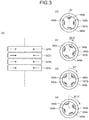
- FIG. 3 is a diagram illustrating a configuration of ultraviolet irradiation units and semiconductor ultraviolet light emitting elements, according to Example 2.
- the ultraviolet irradiation units according to Example 2 are also applicable as the plural ultraviolet irradiation units 320 in the above described ultraviolet irradiation device 300.
- the ultraviolet irradiation units according to Example 2 are formed of first to fourth ultraviolet irradiation units 321b to 324b that irradiate ultraviolet curable resin with ultraviolet light.
- the first to fourth ultraviolet irradiation units 321b to 324b are units of the same type, each unit having four semiconductor ultraviolet light emitting elements 340b arranged on the circumference of the same circle, and as illustrated in FIG. 3(a) , these first to fourth ultraviolet irradiation units 321b to 324b are arranged in a traveling direction of an optical fiber such that the optical fiber passes the centers of the circles.
- illustration of the optical fiber is omitted, but a downward direction on the plane of paper corresponds to the traveling direction of the optical fiber, and a straight line illustrated with a dashed line corresponds to a traveling position of the optical fiber. Further, since the optical fiber passes the centers of the circles on which the semiconductor ultraviolet light emitting elements 340b are arranged, the traveling position of the optical fiber coincides with a central axis of a cylindrical surface defined by arrangement positions of the semiconductor ultraviolet light emitting elements 340b.
- the first to fourth ultraviolet irradiation units 321b to 324b have different arrangements with respect to their circumferential direction angles around an axis that is the traveling direction of the optical fiber. Specifically, with reference to the angle of the first ultraviolet irradiation unit 321b, the angles of the second to fourth ultraviolet irradiation units 322b to 324b are changed respectively by 22.5°, 45°, and 67.5°.
- the semiconductor ultraviolet light emitting elements 340b included in the first to fourth ultraviolet irradiation units 321b to 324b are arranged in a spiral around the axis that is the traveling direction of the optical fiber when the first to fourth ultraviolet irradiation units 321b to 324b are arranged in the traveling direction of the optical fiber. Further, all of the semiconductor ultraviolet light emitting elements 340b included in the first to fourth ultraviolet irradiation units 321b to 324b are at different circumferential direction angles around the axis that is the traveling direction of the optical fiber, and intervals among their circumferential direction angles are equal. As a result, ultraviolet light is emitted evenly with respect to the circumferential direction of the optical fiber, and formation of a satisfactory coating is enabled.
- Arrows drawn in the first to fourth ultraviolet irradiation units 321b to 324b illustrated in FIG. 3(a) indicate emission directions of ultraviolet light emitted from the semiconductor ultraviolet light emitting elements 340b. That is, the semiconductor ultraviolet light emitting elements 340b included in the first to fourth ultraviolet irradiation units 321b to 324b emit ultraviolet light perpendicularly to the axis representing the traveling direction of the optical fiber.
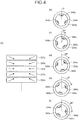
- FIG. 4 is a diagram illustrating a configuration of ultraviolet irradiation units and semiconductor ultraviolet light emitting elements, according to Example 3.
- the ultraviolet irradiation units according to Example 3 are also applicable as the plural ultraviolet irradiation units 320 in the above described ultraviolet irradiation device 300.
- the ultraviolet irradiation units according to Example 3 are formed of first to fifth ultraviolet irradiation units 321c to 325c that irradiate ultraviolet curable resin with ultraviolet light.
- the first to fifth ultraviolet irradiation units 321c to 325c are units of the same type, each unit having three semiconductor ultraviolet light emitting elements 340c arranged on the circumference of the same circle, and as illustrated in FIG. 4(a) , these first to fifth ultraviolet irradiation units 321c to 325c are arranged in a traveling direction of an optical fiber such that the optical fiber passes the centers of the circles.
- illustration of the optical fiber is omitted, but a downward direction on the plane of paper corresponds to the traveling direction of the optical fiber, and a straight line illustrated with a dashed line corresponds to a traveling position of the optical fiber. Further, since the optical fiber passes the centers of the circles on which the semiconductor ultraviolet light emitting elements 340c are arranged, the traveling position of the optical fiber coincides with a central axis of a cylindrical surface defined by arrangement positions of the semiconductor ultraviolet light emitting elements 340c.
- the first to fifth ultraviolet irradiation units 321c to 325c have different arrangements with respect to their circumferential direction angles around an axis that is the traveling direction of the optical fiber. Specifically, with reference to the angle of the first ultraviolet irradiation unit 321c, the angles of the second to fifth ultraviolet irradiation units 322c to 325c are changed respectively by 24°, 48°, 72°, and 96°.
- the semiconductor ultraviolet light emitting elements 340c included in the first to fifth ultraviolet irradiation units 321c to 325c are arranged in a spiral around the axis that is the traveling direction of the optical fiber when the first to fifth ultraviolet irradiation units 321c to 325c are arranged in the traveling direction of the optical fiber. Further, all of the semiconductor ultraviolet light emitting elements 340c included in the first to fifth ultraviolet irradiation units 321c to 325c are at different circumferential direction angles around an axis that is the traveling direction of the optical fiber, and intervals among these circumferential direction angles are equal. As a result, ultraviolet light is emitted evenly with respect to the circumferential direction of the optical fiber, and formation of a satisfactory coating is enabled.
- Arrows drawn in the first to fifth ultraviolet irradiation units 321c to 325c illustrated in FIG. 4(a) indicate emission directions of ultraviolet light emitted from the semiconductor ultraviolet light emitting elements 340c. That is, the semiconductor ultraviolet light emitting elements 340c included in the first to fifth ultraviolet irradiation units 321c to 325c are inclinedly installed in their ultraviolet irradiation units so as to emit ultraviolet light toward the vicinity of a single point on the axis representing the traveling direction of the optical fiber. As will be described in detail with experimental examples later, by the inclined arrangement of these semiconductor ultraviolet light emitting elements 340c, illuminance of ultraviolet light emitted onto the ultraviolet curable resin is increased, and curing of the ultraviolet curable resin is promoted.
- FIG. 5 is a diagram illustrating a configuration of ultraviolet irradiation units and semiconductor ultraviolet light emitting elements, according to Example 4.
- the ultraviolet irradiation units according to Example 4 are also applicable as the plural ultraviolet irradiation units 320 in the above described ultraviolet irradiation device 300.
- the ultraviolet irradiation units according to Example 4 are formed of: first to sixth ultraviolet irradiation units 321d to 326d that irradiate ultraviolet curable resin with ultraviolet light; and a deep ultraviolet irradiation unit 350d that performs irradiation with deep ultraviolet light.
- the first to sixth ultraviolet irradiation units 321d to 326d are units of the same type, each unit having three semiconductor ultraviolet light emitting elements 340d arranged on the circumference of the same circle, and as illustrated in FIG.
- these first to sixth ultraviolet irradiation units 321d to 326d are arranged in a traveling direction of an optical fiber such that the optical fiber passes the centers of the circles. Further, the deep ultraviolet irradiation unit 350d is arranged upstream of (upper than, on the plane of paper) the first ultraviolet irradiation unit 321d.
- the deep ultraviolet irradiation unit 350d has semiconductor ultraviolet light emitting elements provided therein, which emit deep ultraviolet light, and which are, for example, arranged similarly to those in the first ultraviolet irradiation unit 321d.
- Deep ultraviolet light (for example, of wavelength of 200 nm to 350 nm) is shorter in wavelength than normal ultraviolet light (for example, of wavelength of 365 nm to 405 nm), and thus acts on ultraviolet curable resin in a layer shallower than depth reached by normal ultraviolet light. Therefore, arrangement of the deep ultraviolet irradiation unit 350d upstream of the first ultraviolet irradiation unit 321d leads to curing of ultraviolet curable resin in a layer closer to the surface, first. As described already, since ultraviolet curable resins react with oxygen and are not cured sufficiently when they are cured in an atmosphere high in oxygen concentration, by introduction of inert gas, ultraviolet curable resins are prevented from reacting with oxygen. Arranging the deep ultraviolet irradiation unit 350d upstream of the first ultraviolet irradiation unit 321d and curing first the ultraviolet curable resin in a layer closer to the surface that more easily reacts with oxygen contribute to improvement in quality of the surface.
- normal ultraviolet light for example, of wavelength of wavelength of 365 nm to 405
- the ultraviolet irradiation units according to Example 4 may be considered as units having the deep ultraviolet irradiation unit 350d added to the ultraviolet irradiation units according to Example 1. Therefore, the ultraviolet irradiation units according to Example 4 inherit the functions and effects of the ultraviolet irradiation units according to Example 1, as-is.
- FIG. 6 is a diagram illustrating a configuration of ultraviolet irradiation units and semiconductor ultraviolet light emitting elements, according to Example 5.
- the ultraviolet irradiation units according to Example 5 are also applicable as the plural ultraviolet irradiation units 320 in the above described ultraviolet irradiation device 300.
- the ultraviolet irradiation units according to Example 5 are formed of first to fourth ultraviolet irradiation units 321e to 324e that irradiate ultraviolet curable resin with ultraviolet light, and a deep ultraviolet irradiation unit 350e that performs irradiation with deep ultraviolet light.
- the first to fourth ultraviolet irradiation units 321e to 324e are units of the same type, each unit having four semiconductor ultraviolet light emitting elements 340e arranged on the circumference of the same circle, and as illustrated in FIG.
- these first to fourth ultraviolet irradiation units 321e to 324e are arranged in a traveling direction of an optical fiber such that the optical fiber passes the centers of the circles. Further, the deep ultraviolet irradiation unit 350e is arranged upstream of (upper than, on the plane of paper) the first ultraviolet irradiation unit 321e.
- the deep ultraviolet irradiation unit 350e has the same configuration as the deep ultraviolet irradiation unit 350d according to Example 4.
- arrangement of the deep ultraviolet irradiation unit 350e upstream of the first ultraviolet irradiation unit 321e contributes to improvement in quality of the surface, through curing of ultraviolet curable resin in a layer closer to the surface that more easily reacts with oxygen, first.
- the ultraviolet irradiation units according to Example 5 may be considered as units having the deep ultraviolet irradiation unit 350e added to the ultraviolet irradiation units according to Example 2. Therefore, the ultraviolet irradiation units according to Example 5 inherit the functions and effects of the ultraviolet irradiation units according to Example 2, as-is.
- FIG. 7 is a diagram illustrating a configuration of ultraviolet irradiation units and semiconductor ultraviolet light emitting elements, according to Example 6.
- the ultraviolet irradiation units according to Example 6 are also applicable as the plural ultraviolet irradiation units 320 in the above described ultraviolet irradiation device 300.
- the ultraviolet irradiation units according to Example 6 are formed of first to fifth ultraviolet irradiation units 321f to 325f that irradiate ultraviolet curable resin with ultraviolet light, and a deep ultraviolet irradiation unit 350f that performs irradiation with deep ultraviolet light.
- the first to fifth ultraviolet irradiation units 321f to 325f are units of the same type, each unit having three semiconductor ultraviolet light emitting elements 340f arranged on the circumference of the same circle, and as illustrated in FIG.
- these first to fifth ultraviolet irradiation units 321f to 325f are arranged in a traveling direction of an optical fiber such that the optical fiber passes the centers of the circles. Further, the deep ultraviolet irradiation unit 350f is arranged upstream of (upper than, on the plane of paper) the first ultraviolet irradiation unit 321f.
- the deep ultraviolet irradiation unit 350f has the same configuration as the deep ultraviolet irradiation unit 350d according to Example 4.
- arrangement of the deep ultraviolet irradiation unit 350f upstream of the first ultraviolet irradiation unit 321f contributes to improvement in quality of the surface, through curing of ultraviolet curable resin in a layer closer to the surface that more easily reacts with oxygen, first.
- the ultraviolet irradiation units according to Example 6 may be considered as units having the deep ultraviolet irradiation unit 350f added to the ultraviolet irradiation units according to Example 3. Therefore, the ultraviolet irradiation units according to Example 6 inherit the functions and effects of the ultraviolet irradiation units according to Example 3, as-is.
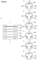
- FIG. 8 is a diagram illustrating a configuration of ultraviolet irradiation units and semiconductor ultraviolet light emitting elements, according to a comparative example.
- This comparative example was used in verification experiments described later and exhibiting effects of the present invention.
- the ultraviolet irradiation units according to the comparative example are also applicable as the plural ultraviolet irradiation units 320 in the above described ultraviolet irradiation device 300.
- the ultraviolet irradiation units according to the comparative example are formed of first to sixth ultraviolet irradiation units 321g to 326g that irradiate ultraviolet curable resin with ultraviolet light.
- the first to sixth ultraviolet irradiation units 321g to 326g are units of the same type, each unit having three semiconductor ultraviolet light emitting elements 340g arranged on the circumference of the same circle, and as illustrated in FIG. 8(a) , these first to sixth ultraviolet irradiation units 321g to 326g are arranged in a traveling direction of an optical fiber such that the optical fiber passes the centers of the circles.
- the configuration of the ultraviolet irradiation units and semiconductor ultraviolet light emitting elements according to the comparative example is about the same as the configuration of the ultraviolet irradiation units and semiconductor ultraviolet light emitting elements according to Example 1, but in this comparative example, as illustrated in FIG. 8(b) to FIG. 8(g) , the first to sixth ultraviolet irradiation units 321g to 326g have the same arrangement with respect to their circumferential direction angles around an axis that is the traveling direction of the optical fiber.
- the semiconductor ultraviolet light emitting elements 340g included in the first to sixth ultraviolet irradiation units 321g to 326g emit ultraviolet light perpendicularly to the axis representing the traveling direction of the optical fiber.
- the semiconductor ultraviolet light emitting elements are arranged in these units themselves.
- a configuration for emission of ultraviolet light emitted from an ultraviolet light source by guidance of the ultraviolet light through an optical fiber or the like may be provided at a position where ultraviolet light is emitted toward ultraviolet curable resin.
- an ultraviolet irradiation device is configured by arrangement of a plurality of such ultraviolet irradiation units similarly to Examples 1 to 6, effects similar to those of Examples 1 to 6 are able to be achieved.
- Table 1 below is a table illustrating results of experiments for verification of effects of bare optical fiber manufacturing methods and ultraviolet irradiation devices, according to the embodiment of the present invention.
- the verification experiments listed in Table 1 were for verification of characteristics of bare optical fibers when the bare optical fibers were manufactured by use of ultraviolet irradiation devices, to which the configurations described in Examples 1 to 6 and the comparative example had been applied.
- a wet-on-dry method was adopted, and for facilitation of verification of the effects, the embodiment of the present invention was applied only to secondary layers. Further, a photopolymerization initiator used in ultraviolet curable resin of the secondary layers was Irgacure 184 (BASF Japan Co., Ltd.).
- Reduction rates of power consumption mean reduction rates of power consumption as compared to the comparative example. Determination on presence of undulation is made by: measuring length of bare optical fibers manufactured, in a state where tension is applied and in a state where tension is not applied; and determining that undulation is present if in a case where the length of a bare optical fiber measured in the state where tension is applied is 30 m, the length of the bare optical fiber measured in the state where tension is not applied is reduced by 5 cm or more.
- the state where tension is applied corresponds to tension when a bare optical fiber is sent out from a bobbin, and 50 g is used.
- FIG. 9 is a schematic diagram illustrating an outline of a knot test implemented.
- a single loop is made with a bare optical fiber F 3 manufactured, the bare optical fiber F 3 is sequentially made to pass through the loop, a circle contacting itself and having a diameter of about 7 cm is made at five places, points A to E, and both ends of this optical fiber are pulled at a speed of 5 mm/minute by a tension tester.
- Loads [N] measured thereby are used as results thereof.
- a cable loss is a loss related to transmission of light of a wavelength of 1.55 ⁇ m in a loose tube type optical fiber cable made by use of a bare optical fiber, and a permissible range of cable loss is 0.230 dB/km or less.
- FIG. 10 is a sectional view illustrating a structure of a loose tube type optical fiber cable, and a cable loss was measured by use of this loose tube type optical fiber cable.
- a loose tube type optical fiber cable F 4 is formed of a tension member 41, colored and coated optical fibers 42, loose tubes 43, jelly 44, and a sheath 45.
- the tension member 41 is made of metal or plastic.
- the loose tubes 43 made of metal or plastic are plurally provided on a cylindrical lateral surface of the tension member 41, with the colored and coated optical fibers 42 inserted through the loose tubes 43. These loose tubes 43 are surrounded by the sheath 45 made of plastic, and gaps among the loose tubes 43 are filled with the jelly 44.
- Values of 2.5% modulus are measured as follows. First, bare optical fibers manufactured by manufacturing methods using ultraviolet irradiation devices, to which the configurations according to Examples 1 to 6 and the comparative example had been applied, were immersed in liquid nitrogen, glass fibers were drawn out therefrom by use of a coating removing tool at a liquid nitrogen temperature, and coating layers were made tubular. With 50 mm lengths of these tubular optical fiber coating layers being samples, 2.5% moduli were measured at a gauge length of 25 mm in conformance to JIS K 7161.
- the bare optical fibers manufactured by use of the ultraviolet irradiation devices, to which the configurations according to Examples 1 to 6 are applied have no undulation, but the bare optical fiber manufactured by use of the ultraviolet irradiation device, to which the configuration according to the comparative example is applied, has undulation.
- ultraviolet light was evenly emitted with respect to the circumferential direction of the optical fibers and satisfactory coatings were formed.
- the bare optical fibers manufactured by use of the ultraviolet irradiation devices, to which the configurations according to Examples 4 to 6 had been applied had significantly improved measurement results for their knot tests.
- the results indicate that in the ultraviolet irradiation devices, to which the configurations according to Examples 4 to 6 had been applied, quality of surfaces of the coatings is improved by curing first the ultraviolet curable resin in layers closer to the surfaces by use of the deep ultraviolet irradiation units.
- the bare optical fibers manufactured by use of the ultraviolet irradiation devices, to which the configurations according to Examples 1 to 6 had been applied were higher in 2.5% modulus than the bare optical fiber manufactured by use of the ultraviolet irradiation device, to which the configuration according to the comparative example had been applied.
- ultraviolet curable resin was sufficiently irradiated with ultraviolet light and satisfactory coatings were formed.
- semiconductor ultraviolet light emitting elements for deep ultraviolet light are also used, but since power consumptions of the semiconductor ultraviolet light emitting elements for deep ultraviolet light are less than those of normal semiconductor ultraviolet light emitting elements, their influence is negligibly small.
- the above described results mean that the ultraviolet irradiation devices, to which the configurations according to Examples 2, 3, 5, and 6 are applied, enable reduction in power consumption in the ultraviolet irradiation devices while maintaining their performance related to the presence of undulation, knot tests, cable losses, and the like.
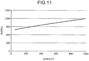
- FIG. 11 is a diagram illustrating a graph representing a relation between: illuminance (I) of ultraviolet light that ultraviolet curable resin is irradiated with; and 2.5% modulus (G). Measurement results illustrated in FIG. 11 are obtained by the following measurement.
- a base material made of quartz glass is prepared, and is spin-coated with an ultraviolet curable resin for a secondary layer in a thickness of 50 ⁇ m.
- the ultraviolet curable resin for a secondary layer is the same resin as that used in the above described comparative experiments for the examples.
- the base material, onto which the ultraviolet curable resin for a secondary layer has been applied, is placed in a purge box, which is then made to have a nitrogen atmosphere, and the resin is cured by irradiation with ultraviolet light (365 nm), with illuminance and speed being adjusted in a conveyor type ultraviolet irradiation device such that a predetermined amount of accumulated light is obtained.
- the cured ultraviolet curable resin for a secondary layer is peeled off from the base material, and cut into a strip having a width of 6 mm for obtainment of a sample having a length of 50 mm or more.
- a 2.5% modulus (elastic modulus) of this sample is measured at a gauge length of 25 mm in conformance to JIS K 7161.
- the semiconductor ultraviolet light emitting elements are configured to emit ultraviolet light toward the vicinity of a single point on the axis representing the traveling direction of the optical fiber, and thus illuminance of ultraviolet light emitted to the ultraviolet curable resin is increased, and a better coating is able to be formed.
- the semiconductor ultraviolet light emitting elements included in the ultraviolet irradiation units are arranged in a spiral around the axis that is the traveling direction of the optical fiber, but the arrangement is not necessarily made spiral, and the semiconductor ultraviolet light emitting elements may be arranged differently in an irregular manner with respect to the circumferential direction angles around the axis that is the traveling direction of the optical fiber.
- a bare optical fiber manufacturing method and an ultraviolet irradiation device, according to the present invention are useful in manufacture of bare optical fibers.
Landscapes
- Chemical & Material Sciences (AREA)
- Life Sciences & Earth Sciences (AREA)
- Engineering & Computer Science (AREA)
- Chemical Kinetics & Catalysis (AREA)
- General Chemical & Material Sciences (AREA)
- Materials Engineering (AREA)
- Organic Chemistry (AREA)
- Physics & Mathematics (AREA)
- General Life Sciences & Earth Sciences (AREA)
- Geochemistry & Mineralogy (AREA)
- Health & Medical Sciences (AREA)
- Toxicology (AREA)
- Oral & Maxillofacial Surgery (AREA)
- Thermal Sciences (AREA)
- Mechanical Engineering (AREA)
- Electromagnetism (AREA)
- Metallurgy (AREA)
- General Engineering & Computer Science (AREA)
- General Physics & Mathematics (AREA)
- Optics & Photonics (AREA)
- Surface Treatment Of Glass Fibres Or Filaments (AREA)
- Optical Fibers, Optical Fiber Cores, And Optical Fiber Bundles (AREA)
- Coating Apparatus (AREA)
Abstract
Description
- The present invention relates to a bare optical fiber manufacturing method, and an ultraviolet irradiation device.
- Generally, optical fibers made of quartz glass and the like have coatings formed on outer peripheral surfaces of the optical fibers thereof (also called glass optical fibers), each of which is made of a core and a cladding. An optical fiber having a coating formed therearound is called a bare optical fiber.
- In a bare optical fiber manufacturing method, generally, a coating is formed on an outer peripheral surface of a glass optical fiber by: manufacture of the glass optical fiber by drawing of an optical fiber preform in a drawing furnace; then, application of ultraviolet curable resin to an outer peripheral surface of the glass optical fiber thereafter in a resin coating device also called dies; and irradiation of the ultraviolet curable resin with ultraviolet light in an ultraviolet irradiation device.
- Conventionally, a high-pressure mercury lamp or a metal halide lamp has generally been used as an ultraviolet light source of an ultraviolet irradiation device in a bare optical fiber manufacturing process. However, for the purpose of reducing maintenance cost and replacement frequency, and reducing power consumption; use of a semiconductor ultraviolet light emitting element, such as a light emitting diode (UV-LED) or a laser diode (UV-LD), which emits ultraviolet light, as an ultraviolet light source to be used in an ultraviolet irradiation device, has been investigated (see, for example,
Patent Literature 1 to Patent Literature 5). -
- Patent Literature 1: Japanese Unexamined Patent Application, Publication No.
2010-117525 - Patent Literature 2: Japanese Unexamined Patent Application, Publication No.
2010-117526 - Patent Literature 3: Japanese Unexamined Patent Application, Publication No.
2010-117527 - Patent Literature 4: Japanese Unexamined Patent Application, Publication No.
2010-117530 - Patent Literature 5: Japanese Unexamined Patent Application, Publication No.
2010-117531 - However, since ultraviolet light emitted from a semiconductor ultraviolet light emitting element has a single wavelength or a wavelength bandwidth narrower than that of a conventional lamp, a problem where the cure degree of resin is reduced is caused. When the cure degree of resin is insufficient, there may be caused problems of sticking or adhesion among bare optical fibers when an optical fiber is wound around a bobbin, and degradation in the transmission characteristics or due to waviness generated in the optical fiber or discoloration of a surface of the optical fiber, or the like.
- The present invention has been made in view of the above, and an object thereof is to provide a bare optical fiber manufacturing method and an ultraviolet irradiation device that enable ultraviolet curable resin to be cured sufficiently even if ultraviolet light of a single wavelength or a narrow wavelength bandwidth is used. Solution to Problem
- In order to solve the above problem(s) and achieve the object, a bare optical fiber manufacturing method according to an embodiment of the present invention is a method of irradiating an ultraviolet curable resin applied around an optical fiber, with ultraviolet light emitted from semiconductor ultraviolet light emitting elements, and curing the ultraviolet curable resin, wherein the ultraviolet curable resin applied around the optical fiber is irradiated with the ultraviolet light by use of an ultraviolet irradiation device having plural ultraviolet irradiation units each having plural positions where the ultraviolet light is emitted toward the ultraviolet curable resin, the plural positions being arranged on a circumference of the same circle, the plural ultraviolet irradiation units being arranged in a traveling direction of the optical fiber such that the optical fiber passes centers of the circles, at least two of the plural ultraviolet irradiation units being differently arranged with respect to circumferential direction angles thereof around an axis that is the traveling direction of the optical fiber.
- In the bare optical fiber manufacturing method according to the embodiment of the present invention, the semiconductor ultraviolet light emitting elements are arranged at the positions in the ultraviolet irradiation units.
- In the bare optical fiber manufacturing method according to the embodiment of the present invention, all of the semiconductor ultraviolet light emitting elements included in the plural ultraviolet irradiation units are at different circumferential direction angles around the axis that is the traveling direction of the optical fiber.
- In the bare optical fiber manufacturing method according to the embodiment of the present invention, the semiconductor ultraviolet light emitting elements included in the plural ultraviolet irradiation units are arranged in a spiral around the axis that is the traveling direction of the optical fiber.
- In the bare optical fiber manufacturing method according to the embodiment of the present invention, the semiconductor ultraviolet light emitting elements included in the plural ultraviolet irradiation units emit ultraviolet light toward the vicinity of a single point on the axis representing the traveling direction of the optical fiber.
- In the bare optical fiber manufacturing method according to the embodiment of the present invention, the ultraviolet irradiation device further includes a deep ultraviolet irradiation unit that emits deep ultraviolet light, the deep ultraviolet irradiation unit being upstream of the plural ultraviolet irradiation units in the raveling direction of the optical fiber, and the ultraviolet curable resin applied around the optical fiber is irradiated with the ultraviolet light after being irradiated with the deep ultraviolet light.
- An ultraviolet irradiation device according to an embodiment of the present invention is a device that irradiates an ultraviolet curable resin applied around an optical fiber, with ultraviolet light emitted from semiconductor ultraviolet light emitting elements, and cures the ultraviolet curable resin. The ultraviolet irradiation device includes plural ultraviolet irradiation units having plural positions where the ultraviolet light is emitted toward the ultraviolet curable resin, the plural positions being arranged on a circumference of the same circle, the plural ultraviolet irradiation units being arranged in a traveling direction of the optical fiber such that the optical fiber passes centers of the circles, wherein at least two of the plural ultraviolet irradiation units are differently arranged with respect to circumferential direction angles thereof around an axis that is the traveling direction of the optical fiber.
- In the ultraviolet irradiation device according to the embodiment of the present invention, the semiconductor ultraviolet light emitting elements are arranged at the positions in the ultraviolet irradiation units.
- In the ultraviolet irradiation device according to the embodiment of the present invention, all of the semiconductor ultraviolet light emitting elements included in the plural ultraviolet irradiation units are at different circumferential direction angles around the axis that is the traveling direction of the optical fiber.
- In the ultraviolet irradiation device according to the embodiment of the present invention, the semiconductor ultraviolet light emitting elements included in the plural ultraviolet irradiation units are arranged in a spiral around the axis that is the traveling direction of the optical fiber.
- In the ultraviolet irradiation device according to the embodiment of the present invention, the semiconductor ultraviolet light emitting elements included in the plural ultraviolet irradiation units are inclinedly installed in the ultraviolet irradiation units so as to emit the ultraviolet light toward the vicinity of a single point on the axis representing the traveling direction of the optical fiber.
- The ultraviolet irradiation device according to the embodiment of the present invention further includes a deep ultraviolet irradiation unit that emits deep ultraviolet light, the deep ultraviolet irradiation unit being upstream of the plural ultraviolet irradiation units in the traveling direction of the optical fiber. Advantageous Effects of Invention
- A bare optical fiber manufacturing method and an ultraviolet irradiation device, according to the present invention, have an effect of enabling ultraviolet curable resin to be cured sufficiently even if ultraviolet light of a single wavelength or a narrow wavelength bandwidth is used.
-
-
FIG. 1 is a schematic block diagram illustrating an overall configuration of a bare optical fiber manufacturing apparatus used in a bare optical fiber manufacturing method according to an embodiment of the present invention. -
FIG. 2 is a diagram illustrating a configuration of ultraviolet irradiation units and semiconductor ultraviolet light emitting elements, according to Example 1. -
FIG. 3 is a diagram illustrating a configuration of ultraviolet irradiation units and semiconductor ultraviolet light emitting elements, according to Example 2. -
FIG. 4 is a diagram illustrating a configuration of ultraviolet irradiation units and semiconductor ultraviolet light emitting elements, according to Example 3. -
FIG. 5 is a diagram illustrating a configuration of ultraviolet irradiation units and semiconductor ultraviolet light emitting elements, according to Example 4. -
FIG. 6 is a diagram illustrating a configuration of ultraviolet irradiation units and semiconductor ultraviolet light emitting elements, according to Example 5. -
FIG. 7 is a diagram illustrating a configuration of ultraviolet irradiation units and semiconductor ultraviolet light emitting elements, according to Example 6. -
FIG. 8 is a diagram illustrating a configuration of ultraviolet irradiation units and semiconductor ultraviolet light emitting elements, according to a comparative example. -
FIG. 9 is a schematic diagram illustrating an outline of a knot test implemented. -
FIG. 10 is a sectional view illustrating a structure of a loose tube type optical fiber cable. -
FIG. 11 is a diagram illustrating a graph representing a relation between: illuminance of ultraviolet light that ultraviolet curable resin is irradiated with; and 2.5% modulus. - Hereinafter, while reference is made to the appended drawings, a bare optical fiber manufacturing method and an ultraviolet irradiation device, according to an embodiment of the present invention, will be described in detail. The present invention is not limited by the embodiment described below. Further, it needs to be noted that the drawings are schematic, relations among dimensions of elements, ratios among the elements, and the like may be different from the actual ones. Furthermore, a portion having different dimensional relations and ratios among the drawings may be included.
-
FIG. 1 is a schematic view illustrating an overall configuration of a bare opticalfiber manufacturing apparatus 1000 used in a bare optical fiber manufacturing method according to the embodiment of the present invention. As illustrated inFIG. 1 , the bare opticalfiber manufacturing apparatus 1000 includes adrawing furnace 100, aresin coating device 200, anultraviolet irradiation device 300, and awinding device 400. - The
drawing furnace 100 is for manufacturing an optical fiber F1 from an optical fiber preform P, and includes aheater 110 for heating the optical fiber preform P. The optical fiber preform P is an intermediate product having, around a region that becomes a core in a final product, a region formed therein, which becomes a cladding. The optical fiber F1 is manufactured by drawing this optical fiber preform P so as to have a standardized outer diameter (for example, 125 µm). - The
heater 110 included in thedrawing furnace 100 heats a lower end of the optical fiber preform P to about 2000°C. The lower end of the optical fiber preform P that has been softened by the heating by theheater 110 is drawn by thewinding device 400 downstream therefrom. Outer diameter of the optical fiber F1 manufactured by thedrawing furnace 100 is adjusted according to temperature of theheater 110, winding speed of thewinding device 400, and the like. - The
resin coating device 200 is a device that applies ultraviolet curable resin around the optical fiber F1, and theultraviolet irradiation device 300 is a device for curing the ultraviolet curable resin applied around the optical fiber F1. Generally, at least two layers of coating, an inner primary layer and an outer secondary layer, are formed around the optical fiber F1. A wet-on-wet method and a wet-on-dry method are known as methods of forming multiple layers of coating around the optical fiber F1. - The wet-on-wet method is a method, in which plural ultraviolet curable resins are applied onto the optical fiber F1 in the
resin coating device 200, and the plural ultraviolet curable resins are cured altogether by ultraviolet irradiation of one time in theultraviolet irradiation device 300. - On the contrary, the wet-on-dry method is a method, in which plural stages each having a pair of the
resin coating device 200 and theultraviolet irradiation device 300 are provided, and coating is formed per layer by theresin coating device 200 and theultraviolet irradiation device 300 of each of these stages. - Therefore, strictly speaking, the bare optical
fiber manufacturing apparatus 1000 illustrated inFIG. 1 has an apparatus configuration of the wet-on-wet method. However, the embodiment of the present invention is not limited to the bare opticalfiber manufacturing apparatus 1000 of the wet-on-wet method. Even if the bare opticalfiber manufacturing apparatus 1000 is of the wet-on-dry method, the embodiment of the present invention is applicable to at least one of, or preferably all of, the plural stages each having the pair of theresin coating device 200 and theultraviolet irradiation device 300. Simply for avoidance of redundant description, the embodiment of the present invention will be described herein by use of the configuration of the bare opticalfiber manufacturing apparatus 1000 including only one pair of theresin coating device 200 and theultraviolet irradiation device 300. - As illustrated in
FIG. 1 , theresin coating device 200 is configured such that the optical fiber F1 manufactured by the drawingfurnace 100 passes inside theresin coating device 200. When the optical fiber F1 passes inside theresin coating device 200, an ultraviolet curable resin for a primary layer, and/or an ultraviolet curable resin for a secondary layer are/is applied to the optical fiber F1. - The ultraviolet curable resin is, for example, a resin having at least two ethylenically unsaturated groups that are polymerized and cured by ultraviolet light, and preferably an oligomer is used as the ultraviolet curable resin. The oligomer is a polymer having a degree of polymerization of 2 to 100. Further, the ultraviolet curable resin has a photopolymerization initiator, for which examples will be described later, added therein.
- Further, in addition to the oligomer and the photopolymerization initiator, the ultraviolet curable resin may contain any of, for example: a diluent monomer, a photosensitizer, a silane coupling agent, a chain transfer agent, and various additives. As the diluent monomer, a monofunctional (meth)acrylate or a polyfunctional (meth)acrylate is used. The diluent monomer means a monomer for dilution of the ultraviolet curable resin.
- If a wavelength region of light emitted by a semiconductor ultraviolet light emitting element light source is 350 nm to 405 nm, the following may be used as the photopolymerization initiator having ultraviolet absorption in this wavelength region and capable of suitably curing a composition.
- For example, the photopolymerization initiator may be any of: 2-methyl-1-[4-(methylthio)phenyl]-2-morpholinopropanone-1,2-benzyl-2-dimethylamino-1-(4-morpholinophenyl)-butan-1-one; 2-(dimethylamino)-2-[(4-methylphenyl)methyl]-1-[4-(4-morpholinyl)phenyl]-1-butanone; N,N-dimethylaminoacetophenone, and the like, which are of the α-aminoketone type. Commercialized products thereof include Irgacure 907, Irgacure 369, Irgacure 379 (in trade names, manufactured by BASF Japan Co., Ltd.), and the like. "Irgacure" is a trademark of BASF Japan Co., Ltd.
- Or, the photopolymerization initiator may be any of: 2,4,6-trimethylbenzoyldiphenylphosphine oxide; bis(2,4,6-trimethylbenzoyl)-phenylphosphine oxide; bis(2,6-dimethoxybenzoyl)-2,4,4-trimethyl-pentylphosphine oxide, and the like, which are of the acylphosphine oxide type. Commercialized products thereof include Irgacure 819, Lucirin TPO, Lucirin TPO-L, Irgacure 2100 (in trade names, manufactured by BASF Japan Co., Ltd.), and the like.
- Or, the photopolymerization initiator may be any of: commercialized products, Irgacure OXE 01 and Irgacure OXE 02 (in trade names, manufactured by BASF Japan Co., Ltd.), which are of the O-acyloxime type.
- As illustrated in
FIG. 1 , theultraviolet irradiation device 300 is configured such that the optical fiber F1, to which the ultraviolet curable resin has been applied by theresin coating device 200, passes inside theultraviolet irradiation device 300. The optical fiber F1 is irradiated with ultraviolet light when the optical fiber F1 passes inside theultraviolet irradiation device 300, and the ultraviolet curable resin applied thereon is cured. - The
ultraviolet irradiation device 300 includes atransparent tube 310, pluralultraviolet irradiation units 320, and an inertgas introducing tube 331. Thetransparent tube 310 has transparency to ultraviolet light, and is configured such that the optical fiber F1 passes near a central axis of thetransparent tube 310 in a longitudinal direction thereof. Theultraviolet irradiation units 320 each have semiconductor ultraviolet light emitting elements that irradiate the optical fiber F1 passing inside thetransparent tube 310, with ultraviolet light or deep ultraviolet light. As described as Examples later, any of plural types of configurations may be adopted as a configuration of theultraviolet irradiation units 320 and the semiconductor ultraviolet light emitting elements. - Deep ultraviolet light is a part of ultraviolet light, and will be defined herein as follows. Ultraviolet light having wavelength of 365 nm to 405 nm will simply be referred to as ultraviolet light, and ultraviolet light having wavelength of 200 nm to 350 nm will be referred to as deep ultraviolet light. However, "
ultraviolet irradiation units 320" is a common name for plural ultraviolet irradiation units, and thus include those having semiconductor ultraviolet light emitting elements that emit ultraviolet light, and those having semiconductor ultraviolet light emitting elements that emit deep ultraviolet light. - The inert
gas introducing tube 331 is for filling inert gas inside thetransparent tube 310. Generally, when ultraviolet curable resin is cured under an atmosphere high in oxygen (O2) concentration, the ultraviolet curable resin reacts with oxygen and thus may be cured insufficiently. In order to prevent this, inert gas is supplied into thetransparent tube 310 from the inertgas introducing tube 331, and the atmosphere inside thetransparent tube 310 is decreased in oxygen concentration. The type of the inert gas is not limited as long as the inert gas is inert toward the optical fiber F1 and the ultraviolet curable resin applied to the optical fiber F1, but it is simple to use nitrogen (N2). - The optical fiber F1, in which the ultraviolet curable resin applied therearound has been cured by the
ultraviolet irradiation device 300, is wound up as a bare optical fiber F2, by the windingdevice 400. The windingdevice 400 includesguide rollers drum 430. The illustrated example of the windingdevice 400 is just an example of its configuration, and the number and arrangement of rollers may be modified. As described already, by adjusting the speed, at which the windingdevice 400 winds up the bare optical fiber F2, the windingdevice 400 controls the outer diameter of the optical fiber F1 manufactured by the drawingfurnace 100. - As described above, the bare optical
fiber manufacturing apparatus 1000 illustrated inFIG. 1 is an apparatus that is able to manufacture the bare optical fiber F2 by irradiating ultraviolet curable resin applied around the optical fiber F1, with ultraviolet light emitted from the semiconductor ultraviolet light emitting elements, and curing the ultraviolet curable resin. - Hereinafter, examples of a configuration of ultraviolet irradiation units and semiconductor ultraviolet light emitting elements in an ultraviolet irradiation device will be described.
-
FIG. 2 is a diagram illustrating a configuration of ultraviolet irradiation units and semiconductor ultraviolet light emitting elements, according to Example 1. The ultraviolet irradiation units according to Example 1 are applicable as the pluralultraviolet irradiation units 320 in the above describedultraviolet irradiation device 300. Therefore, for avoidance of redundant explanation, inFIG. 2 , only the configuration and arrangement of the ultraviolet irradiation units and semiconductor ultraviolet light emitting elements are illustrated, and illustration of the other components is omitted. - As illustrated in
FIG. 2 , the ultraviolet irradiation units according to Example 1 are formed of first to sixthultraviolet irradiation units 321a to 326a that irradiate ultraviolet curable resin with ultraviolet light. As illustrated inFIG. 2(b) to FIG. 2(g) , the first to sixthultraviolet irradiation units 321a to 326a are units of the same type, each unit having three semiconductor ultravioletlight emitting elements 340a arranged on the circumference of the same circle, and as illustrated inFIG. 2(a) , these first to sixthultraviolet irradiation units 321a to 326a are arranged in a traveling direction of an optical fiber such that the optical fiber passes the centers of the circles. - In
FIG. 2(a) , illustration of the optical fiber is omitted, but a downward direction on the plane of paper corresponds to the traveling direction of the optical fiber, and a straight line illustrated with a dashed line corresponds to a traveling position of the optical fiber. Further, since the optical fiber passes the centers of the circles on which the semiconductor ultravioletlight emitting elements 340a are arranged, the traveling position of the optical fiber coincides with a central axis of a cylindrical surface defined by arrangement positions of the semiconductor ultravioletlight emitting elements 340a. - As illustrated in
FIG. 2(b) to FIG. 2(g) , the first to sixthultraviolet irradiation units 321a to 326a have different arrangements with respect to their circumferential direction angles around an axis that is the traveling direction of the optical fiber. Specifically, with reference to the angle of the firstultraviolet irradiation unit 321a, the angles of the second to sixthultraviolet irradiation units 322a to 326a are changed respectively by 20°, 40°, 60°, 80°, and 100°. - Therefore, the semiconductor ultraviolet
light emitting elements 340a included in the first to sixthultraviolet irradiation units 321a to 326a are arranged in a spiral around the axis that is the traveling direction of the optical fiber when the first to sixthultraviolet irradiation units 321a to 326a are arranged in the traveling direction of the optical fiber. Further, all of the semiconductor ultravioletlight emitting elements 340a included in the first to sixthultraviolet irradiation units 321a to 326a are at different circumferential direction angles around the axis that is the traveling direction of the optical fiber, and intervals among their circumferential direction angles are equal. As a result, ultraviolet light is emitted evenly with respect to the circumferential direction of the optical fiber, and formation of a satisfactory coating is enabled. - Arrows drawn in the first to sixth
ultraviolet irradiation units 321a to 326a illustrated inFIG. 2(a) indicate emission directions of ultraviolet light emitted from the semiconductor ultravioletlight emitting elements 340a. That is, the semiconductor ultravioletlight emitting elements 340a included in the first to sixthultraviolet irradiation units 321a to 326a emit ultraviolet light perpendicularly to the axis representing the traveling direction of the optical fiber. -
FIG. 3 is a diagram illustrating a configuration of ultraviolet irradiation units and semiconductor ultraviolet light emitting elements, according to Example 2. The ultraviolet irradiation units according to Example 2 are also applicable as the pluralultraviolet irradiation units 320 in the above describedultraviolet irradiation device 300. - As illustrated in
FIG. 3 , the ultraviolet irradiation units according to Example 2 are formed of first to fourthultraviolet irradiation units 321b to 324b that irradiate ultraviolet curable resin with ultraviolet light. As illustrated inFIG. 3(b) to FIG. 3(e) , the first to fourthultraviolet irradiation units 321b to 324b are units of the same type, each unit having four semiconductor ultravioletlight emitting elements 340b arranged on the circumference of the same circle, and as illustrated inFIG. 3(a) , these first to fourthultraviolet irradiation units 321b to 324b are arranged in a traveling direction of an optical fiber such that the optical fiber passes the centers of the circles. - In
FIG. 3(a) , illustration of the optical fiber is omitted, but a downward direction on the plane of paper corresponds to the traveling direction of the optical fiber, and a straight line illustrated with a dashed line corresponds to a traveling position of the optical fiber. Further, since the optical fiber passes the centers of the circles on which the semiconductor ultravioletlight emitting elements 340b are arranged, the traveling position of the optical fiber coincides with a central axis of a cylindrical surface defined by arrangement positions of the semiconductor ultravioletlight emitting elements 340b. - As illustrated in
FIG. 3(b) to FIG. 3(e) , the first to fourthultraviolet irradiation units 321b to 324b have different arrangements with respect to their circumferential direction angles around an axis that is the traveling direction of the optical fiber. Specifically, with reference to the angle of the firstultraviolet irradiation unit 321b, the angles of the second to fourthultraviolet irradiation units 322b to 324b are changed respectively by 22.5°, 45°, and 67.5°. - Therefore, the semiconductor ultraviolet
light emitting elements 340b included in the first to fourthultraviolet irradiation units 321b to 324b are arranged in a spiral around the axis that is the traveling direction of the optical fiber when the first to fourthultraviolet irradiation units 321b to 324b are arranged in the traveling direction of the optical fiber. Further, all of the semiconductor ultravioletlight emitting elements 340b included in the first to fourthultraviolet irradiation units 321b to 324b are at different circumferential direction angles around the axis that is the traveling direction of the optical fiber, and intervals among their circumferential direction angles are equal. As a result, ultraviolet light is emitted evenly with respect to the circumferential direction of the optical fiber, and formation of a satisfactory coating is enabled. - Arrows drawn in the first to fourth
ultraviolet irradiation units 321b to 324b illustrated inFIG. 3(a) indicate emission directions of ultraviolet light emitted from the semiconductor ultravioletlight emitting elements 340b. That is, the semiconductor ultravioletlight emitting elements 340b included in the first to fourthultraviolet irradiation units 321b to 324b emit ultraviolet light perpendicularly to the axis representing the traveling direction of the optical fiber. -
FIG. 4 is a diagram illustrating a configuration of ultraviolet irradiation units and semiconductor ultraviolet light emitting elements, according to Example 3. The ultraviolet irradiation units according to Example 3 are also applicable as the pluralultraviolet irradiation units 320 in the above describedultraviolet irradiation device 300. - As illustrated in
FIG. 4 , the ultraviolet irradiation units according to Example 3 are formed of first to fifthultraviolet irradiation units 321c to 325c that irradiate ultraviolet curable resin with ultraviolet light. As illustrated inFIG. 4(b) to FIG. 4(f) , the first to fifthultraviolet irradiation units 321c to 325c are units of the same type, each unit having three semiconductor ultravioletlight emitting elements 340c arranged on the circumference of the same circle, and as illustrated inFIG. 4(a) , these first to fifthultraviolet irradiation units 321c to 325c are arranged in a traveling direction of an optical fiber such that the optical fiber passes the centers of the circles. - In
FIG. 4(a) , illustration of the optical fiber is omitted, but a downward direction on the plane of paper corresponds to the traveling direction of the optical fiber, and a straight line illustrated with a dashed line corresponds to a traveling position of the optical fiber. Further, since the optical fiber passes the centers of the circles on which the semiconductor ultravioletlight emitting elements 340c are arranged, the traveling position of the optical fiber coincides with a central axis of a cylindrical surface defined by arrangement positions of the semiconductor ultravioletlight emitting elements 340c. - As illustrated in
FIG. 4(b) to FIG. 4(f) , the first to fifthultraviolet irradiation units 321c to 325c have different arrangements with respect to their circumferential direction angles around an axis that is the traveling direction of the optical fiber. Specifically, with reference to the angle of the firstultraviolet irradiation unit 321c, the angles of the second to fifthultraviolet irradiation units 322c to 325c are changed respectively by 24°, 48°, 72°, and 96°. - Therefore, the semiconductor ultraviolet
light emitting elements 340c included in the first to fifthultraviolet irradiation units 321c to 325c are arranged in a spiral around the axis that is the traveling direction of the optical fiber when the first to fifthultraviolet irradiation units 321c to 325c are arranged in the traveling direction of the optical fiber. Further, all of the semiconductor ultravioletlight emitting elements 340c included in the first to fifthultraviolet irradiation units 321c to 325c are at different circumferential direction angles around an axis that is the traveling direction of the optical fiber, and intervals among these circumferential direction angles are equal. As a result, ultraviolet light is emitted evenly with respect to the circumferential direction of the optical fiber, and formation of a satisfactory coating is enabled. - Arrows drawn in the first to fifth
ultraviolet irradiation units 321c to 325c illustrated inFIG. 4(a) indicate emission directions of ultraviolet light emitted from the semiconductor ultravioletlight emitting elements 340c. That is, the semiconductor ultravioletlight emitting elements 340c included in the first to fifthultraviolet irradiation units 321c to 325c are inclinedly installed in their ultraviolet irradiation units so as to emit ultraviolet light toward the vicinity of a single point on the axis representing the traveling direction of the optical fiber. As will be described in detail with experimental examples later, by the inclined arrangement of these semiconductor ultravioletlight emitting elements 340c, illuminance of ultraviolet light emitted onto the ultraviolet curable resin is increased, and curing of the ultraviolet curable resin is promoted. -
FIG. 5 is a diagram illustrating a configuration of ultraviolet irradiation units and semiconductor ultraviolet light emitting elements, according to Example 4. The ultraviolet irradiation units according to Example 4 are also applicable as the pluralultraviolet irradiation units 320 in the above describedultraviolet irradiation device 300. - As illustrated in
FIG. 5 , the ultraviolet irradiation units according to Example 4 are formed of: first to sixthultraviolet irradiation units 321d to 326d that irradiate ultraviolet curable resin with ultraviolet light; and a deepultraviolet irradiation unit 350d that performs irradiation with deep ultraviolet light. As illustrated inFIG. 5(b) to FIG. 5(g) , the first to sixthultraviolet irradiation units 321d to 326d are units of the same type, each unit having three semiconductor ultravioletlight emitting elements 340d arranged on the circumference of the same circle, and as illustrated inFIG. 5(a) , these first to sixthultraviolet irradiation units 321d to 326d are arranged in a traveling direction of an optical fiber such that the optical fiber passes the centers of the circles. Further, the deepultraviolet irradiation unit 350d is arranged upstream of (upper than, on the plane of paper) the firstultraviolet irradiation unit 321d. The deepultraviolet irradiation unit 350d has semiconductor ultraviolet light emitting elements provided therein, which emit deep ultraviolet light, and which are, for example, arranged similarly to those in the firstultraviolet irradiation unit 321d. - Deep ultraviolet light (for example, of wavelength of 200 nm to 350 nm) is shorter in wavelength than normal ultraviolet light (for example, of wavelength of 365 nm to 405 nm), and thus acts on ultraviolet curable resin in a layer shallower than depth reached by normal ultraviolet light. Therefore, arrangement of the deep
ultraviolet irradiation unit 350d upstream of the firstultraviolet irradiation unit 321d leads to curing of ultraviolet curable resin in a layer closer to the surface, first. As described already, since ultraviolet curable resins react with oxygen and are not cured sufficiently when they are cured in an atmosphere high in oxygen concentration, by introduction of inert gas, ultraviolet curable resins are prevented from reacting with oxygen. Arranging the deepultraviolet irradiation unit 350d upstream of the firstultraviolet irradiation unit 321d and curing first the ultraviolet curable resin in a layer closer to the surface that more easily reacts with oxygen contribute to improvement in quality of the surface. - The ultraviolet irradiation units according to Example 4 may be considered as units having the deep
ultraviolet irradiation unit 350d added to the ultraviolet irradiation units according to Example 1. Therefore, the ultraviolet irradiation units according to Example 4 inherit the functions and effects of the ultraviolet irradiation units according to Example 1, as-is. -
FIG. 6 is a diagram illustrating a configuration of ultraviolet irradiation units and semiconductor ultraviolet light emitting elements, according to Example 5. The ultraviolet irradiation units according to Example 5 are also applicable as the pluralultraviolet irradiation units 320 in the above describedultraviolet irradiation device 300. - As illustrated in
FIG. 6 , the ultraviolet irradiation units according to Example 5 are formed of first to fourthultraviolet irradiation units 321e to 324e that irradiate ultraviolet curable resin with ultraviolet light, and a deepultraviolet irradiation unit 350e that performs irradiation with deep ultraviolet light. As illustrated inFIG. 6(b) to FIG. 6(e) , the first to fourthultraviolet irradiation units 321e to 324e are units of the same type, each unit having four semiconductor ultravioletlight emitting elements 340e arranged on the circumference of the same circle, and as illustrated inFIG. 6(a) , these first to fourthultraviolet irradiation units 321e to 324e are arranged in a traveling direction of an optical fiber such that the optical fiber passes the centers of the circles. Further, the deepultraviolet irradiation unit 350e is arranged upstream of (upper than, on the plane of paper) the firstultraviolet irradiation unit 321e. The deepultraviolet irradiation unit 350e has the same configuration as the deepultraviolet irradiation unit 350d according to Example 4. - Similarly to Example 4, arrangement of the deep
ultraviolet irradiation unit 350e upstream of the firstultraviolet irradiation unit 321e contributes to improvement in quality of the surface, through curing of ultraviolet curable resin in a layer closer to the surface that more easily reacts with oxygen, first. - The ultraviolet irradiation units according to Example 5 may be considered as units having the deep
ultraviolet irradiation unit 350e added to the ultraviolet irradiation units according to Example 2. Therefore, the ultraviolet irradiation units according to Example 5 inherit the functions and effects of the ultraviolet irradiation units according to Example 2, as-is. -
FIG. 7 is a diagram illustrating a configuration of ultraviolet irradiation units and semiconductor ultraviolet light emitting elements, according to Example 6. The ultraviolet irradiation units according to Example 6 are also applicable as the pluralultraviolet irradiation units 320 in the above describedultraviolet irradiation device 300. - As illustrated in
FIG. 7 , the ultraviolet irradiation units according to Example 6 are formed of first to fifthultraviolet irradiation units 321f to 325f that irradiate ultraviolet curable resin with ultraviolet light, and a deepultraviolet irradiation unit 350f that performs irradiation with deep ultraviolet light. As illustrated inFIG. 7(b) to FIG. 7(f) , the first to fifthultraviolet irradiation units 321f to 325f are units of the same type, each unit having three semiconductor ultravioletlight emitting elements 340f arranged on the circumference of the same circle, and as illustrated inFIG. 7(a) , these first to fifthultraviolet irradiation units 321f to 325f are arranged in a traveling direction of an optical fiber such that the optical fiber passes the centers of the circles. Further, the deepultraviolet irradiation unit 350f is arranged upstream of (upper than, on the plane of paper) the firstultraviolet irradiation unit 321f. The deepultraviolet irradiation unit 350f has the same configuration as the deepultraviolet irradiation unit 350d according to Example 4. - Similarly to Example 4, arrangement of the deep
ultraviolet irradiation unit 350f upstream of the firstultraviolet irradiation unit 321f contributes to improvement in quality of the surface, through curing of ultraviolet curable resin in a layer closer to the surface that more easily reacts with oxygen, first. - The ultraviolet irradiation units according to Example 6 may be considered as units having the deep
ultraviolet irradiation unit 350f added to the ultraviolet irradiation units according to Example 3. Therefore, the ultraviolet irradiation units according to Example 6 inherit the functions and effects of the ultraviolet irradiation units according to Example 3, as-is. -
FIG. 8 is a diagram illustrating a configuration of ultraviolet irradiation units and semiconductor ultraviolet light emitting elements, according to a comparative example. This comparative example was used in verification experiments described later and exhibiting effects of the present invention. The ultraviolet irradiation units according to the comparative example are also applicable as the pluralultraviolet irradiation units 320 in the above describedultraviolet irradiation device 300. - As illustrated in
FIG. 8 , the ultraviolet irradiation units according to the comparative example are formed of first to sixthultraviolet irradiation units 321g to 326g that irradiate ultraviolet curable resin with ultraviolet light. As illustrated inFIG. 8(b) to FIG. 8(g) , the first to sixthultraviolet irradiation units 321g to 326g are units of the same type, each unit having three semiconductor ultravioletlight emitting elements 340g arranged on the circumference of the same circle, and as illustrated inFIG. 8(a) , these first to sixthultraviolet irradiation units 321g to 326g are arranged in a traveling direction of an optical fiber such that the optical fiber passes the centers of the circles. - Therefore, the configuration of the ultraviolet irradiation units and semiconductor ultraviolet light emitting elements according to the comparative example is about the same as the configuration of the ultraviolet irradiation units and semiconductor ultraviolet light emitting elements according to Example 1, but in this comparative example, as illustrated in
FIG. 8(b) to FIG. 8(g) , the first to sixthultraviolet irradiation units 321g to 326g have the same arrangement with respect to their circumferential direction angles around an axis that is the traveling direction of the optical fiber. The semiconductor ultravioletlight emitting elements 340g included in the first to sixthultraviolet irradiation units 321g to 326g emit ultraviolet light perpendicularly to the axis representing the traveling direction of the optical fiber. - In the ultraviolet irradiation units or the deep ultraviolet irradiation units described in Examples 1 to 6, the semiconductor ultraviolet light emitting elements are arranged in these units themselves. However, a configuration for emission of ultraviolet light emitted from an ultraviolet light source by guidance of the ultraviolet light through an optical fiber or the like may be provided at a position where ultraviolet light is emitted toward ultraviolet curable resin. When an ultraviolet irradiation device is configured by arrangement of a plurality of such ultraviolet irradiation units similarly to Examples 1 to 6, effects similar to those of Examples 1 to 6 are able to be achieved.
- Table 1 below is a table illustrating results of experiments for verification of effects of bare optical fiber manufacturing methods and ultraviolet irradiation devices, according to the embodiment of the present invention. The verification experiments listed in Table 1 were for verification of characteristics of bare optical fibers when the bare optical fibers were manufactured by use of ultraviolet irradiation devices, to which the configurations described in Examples 1 to 6 and the comparative example had been applied.
- As a method of forming coatings around the optical fibers, a wet-on-dry method was adopted, and for facilitation of verification of the effects, the embodiment of the present invention was applied only to secondary layers. Further, a photopolymerization initiator used in ultraviolet curable resin of the secondary layers was Irgacure 184 (BASF Japan Co., Ltd.).
-
Table 1 Example 1 Example 2 Example 3 Example 4 Example 5 Example 6 Comparative Example Spiral A rrangemen t Yes Yes Yes Yes Yes Yes No Number Of Elements counts/unit 3 4 3 3 4 3 3 Condensing by Elements No No Yes No No Yes No deep-UV No No No Yes Yes Yes No Number Of Units counts 6 4 5 6 4 5 6 Power Consumption Reduction Rate % 0 12 20 0 12 20 - Presence of Undulation Not present Not present Not present Not present Not present Not present Present knot test N 0.095 0.084 0.088 0.051 0.042 0.035 0.091 Cable Loss dB/km 0.226 0.221 0.216 0.194 0.190 0.187 0.228 2.5% Modulus MPa 1011 964 998 1056 978 1007 789 - As illustrated in Table 1, in the verification experiments, reduction rates of power consumption, presence of undulation, knot tests, cable losses, and 2.5% moduli were compared. Reduction rates of power consumption mean reduction rates of power consumption as compared to the comparative example. Determination on presence of undulation is made by: measuring length of bare optical fibers manufactured, in a state where tension is applied and in a state where tension is not applied; and determining that undulation is present if in a case where the length of a bare optical fiber measured in the state where tension is applied is 30 m, the length of the bare optical fiber measured in the state where tension is not applied is reduced by 5 cm or more. The state where tension is applied corresponds to tension when a bare optical fiber is sent out from a bobbin, and 50 g is used.
- A knot test is evaluation of kinetic friction of a surface of a bare optical fiber.
FIG. 9 is a schematic diagram illustrating an outline of a knot test implemented. In this measurement method, as illustrated inFIG. 9 , a single loop is made with a bare optical fiber F3 manufactured, the bare optical fiber F3 is sequentially made to pass through the loop, a circle contacting itself and having a diameter of about 7 cm is made at five places, points A to E, and both ends of this optical fiber are pulled at a speed of 5 mm/minute by a tension tester. Loads [N] measured thereby are used as results thereof. - Further, a cable loss is a loss related to transmission of light of a wavelength of 1.55 µm in a loose tube type optical fiber cable made by use of a bare optical fiber, and a permissible range of cable loss is 0.230 dB/km or less.
FIG. 10 is a sectional view illustrating a structure of a loose tube type optical fiber cable, and a cable loss was measured by use of this loose tube type optical fiber cable. As illustrated inFIG. 10 , a loose tube type optical fiber cable F4 is formed of atension member 41, colored and coatedoptical fibers 42,loose tubes 43,jelly 44, and asheath 45. Thetension member 41 is made of metal or plastic. Theloose tubes 43 made of metal or plastic are plurally provided on a cylindrical lateral surface of thetension member 41, with the colored and coatedoptical fibers 42 inserted through theloose tubes 43. Theseloose tubes 43 are surrounded by thesheath 45 made of plastic, and gaps among theloose tubes 43 are filled with thejelly 44. - Values of 2.5% modulus (elastic modulus) are measured as follows. First, bare optical fibers manufactured by manufacturing methods using ultraviolet irradiation devices, to which the configurations according to Examples 1 to 6 and the comparative example had been applied, were immersed in liquid nitrogen, glass fibers were drawn out therefrom by use of a coating removing tool at a liquid nitrogen temperature, and coating layers were made tubular. With 50 mm lengths of these tubular optical fiber coating layers being samples, 2.5% moduli were measured at a gauge length of 25 mm in conformance to JIS K 7161.
- As understood from Table 1, the bare optical fibers manufactured by use of the ultraviolet irradiation devices, to which the configurations according to Examples 1 to 6 are applied, have no undulation, but the bare optical fiber manufactured by use of the ultraviolet irradiation device, to which the configuration according to the comparative example is applied, has undulation. This indicates that in the ultraviolet irradiation devices, to which the configurations according to Examples 1 to 6 are applied, ultraviolet light was evenly emitted with respect to the circumferential direction of the optical fibers and satisfactory coatings were formed.
- Further, as understood from Table 1, the bare optical fibers manufactured by use of the ultraviolet irradiation devices, to which the configurations according to Examples 4 to 6 had been applied, had significantly improved measurement results for their knot tests. The results indicate that in the ultraviolet irradiation devices, to which the configurations according to Examples 4 to 6 had been applied, quality of surfaces of the coatings is improved by curing first the ultraviolet curable resin in layers closer to the surfaces by use of the deep ultraviolet irradiation units.
- Further, as understood from Table 1, the bare optical fibers manufactured by use of the ultraviolet irradiation devices, to which the configurations according to Examples 1 to 6 had been applied, had satisfactory values for cable loss.
- Further, as understood from Table 1, the bare optical fibers manufactured by use of the ultraviolet irradiation devices, to which the configurations according to Examples 1 to 6 had been applied, were higher in 2.5% modulus than the bare optical fiber manufactured by use of the ultraviolet irradiation device, to which the configuration according to the comparative example had been applied. This indicates that in the ultraviolet irradiation devices, to which the configurations according to Examples 1 to 6 had been applied, ultraviolet curable resin was sufficiently irradiated with ultraviolet light and satisfactory coatings were formed.
- As understood from Table 1, power consumptions of the ultraviolet irradiation devices, to which the configurations according to Examples 2, 3, 5, and 6 had been applied, were less than that of the ultraviolet irradiation device, to which the configuration according to the comparative example had been applied. This is because the number of semiconductor ultraviolet light emitting elements used in each of the ultraviolet irradiation devices, to which the configurations according to Examples 2, 3, 5, and 6 had been applied, was less than the number of semiconductor ultraviolet light emitting elements used in the ultraviolet irradiation device, to which the configuration according to the comparative example had been applied. In the ultraviolet irradiation devices, to which the configurations according to Examples 5 and 6 are applied, semiconductor ultraviolet light emitting elements for deep ultraviolet light are also used, but since power consumptions of the semiconductor ultraviolet light emitting elements for deep ultraviolet light are less than those of normal semiconductor ultraviolet light emitting elements, their influence is negligibly small.
- The above described results mean that the ultraviolet irradiation devices, to which the configurations according to Examples 2, 3, 5, and 6 are applied, enable reduction in power consumption in the ultraviolet irradiation devices while maintaining their performance related to the presence of undulation, knot tests, cable losses, and the like.
- Results of the verification experiments related to advantages of the configurations according to Examples 3 and 6 will now be described. In each of the configurations according to Examples 3 and 6, the semiconductor ultraviolet light emitting elements are arranged to emit ultraviolet light toward the vicinity of a single point on the axis representing the traveling direction of the optical fiber. How this arrangement contributes to curing of the coating will be described.
-
FIG. 11 is a diagram illustrating a graph representing a relation between: illuminance (I) of ultraviolet light that ultraviolet curable resin is irradiated with; and 2.5% modulus (G). Measurement results illustrated inFIG. 11 are obtained by the following measurement. - A base material made of quartz glass is prepared, and is spin-coated with an ultraviolet curable resin for a secondary layer in a thickness of 50 µm. The ultraviolet curable resin for a secondary layer is the same resin as that used in the above described comparative experiments for the examples. The base material, onto which the ultraviolet curable resin for a secondary layer has been applied, is placed in a purge box, which is then made to have a nitrogen atmosphere, and the resin is cured by irradiation with ultraviolet light (365 nm), with illuminance and speed being adjusted in a conveyor type ultraviolet irradiation device such that a predetermined amount of accumulated light is obtained.
- The cured ultraviolet curable resin for a secondary layer is peeled off from the base material, and cut into a strip having a width of 6 mm for obtainment of a sample having a length of 50 mm or more. A 2.5% modulus (elastic modulus) of this sample is measured at a gauge length of 25 mm in conformance to JIS K 7161.
- As understood from the graph illustrated in
FIG. 11 , the higher the illuminance of ultraviolet light that the ultraviolet curable resin is irradiated with, the higher the 2.5% modulus is. Therefore, for an ultraviolet irradiation device, a configuration enabling increase in illuminance of ultraviolet light emitted to an ultraviolet curable resin is preferably adopted for formation of a better coating. In each of the configurations of the ultraviolet irradiation devices according to Examples 3 and 6, the semiconductor ultraviolet light emitting elements are configured to emit ultraviolet light toward the vicinity of a single point on the axis representing the traveling direction of the optical fiber, and thus illuminance of ultraviolet light emitted to the ultraviolet curable resin is increased, and a better coating is able to be formed. - The embodiment of the present invention has been specifically described above, but the present invention is not limited to the above described embodiment, and various modifications based on technical ideas of the present invention are possible. For example, in each of Examples 1 to 6 described above, all of the ultraviolet irradiation units have different arrangements with respect to their circumferential direction angles around the axis that is the traveling direction of the optical fiber, but as long as at least two of the ultraviolet irradiation units have different arrangements with respect to their circumferential direction angles around the axis that is the traveling direction of the optical fiber, a coating better than that of the comparative example is able to be formed.
- Further, in each of Examples 1 to 6 described above, the semiconductor ultraviolet light emitting elements included in the ultraviolet irradiation units are arranged in a spiral around the axis that is the traveling direction of the optical fiber, but the arrangement is not necessarily made spiral, and the semiconductor ultraviolet light emitting elements may be arranged differently in an irregular manner with respect to the circumferential direction angles around the axis that is the traveling direction of the optical fiber.
- Further, although comparative experiments focused only on the secondary layers were performed as the above described comparative experiments for Examples 1 to 6, the embodiment of the present invention may be applied to primary layers.
- As described above, a bare optical fiber manufacturing method and an ultraviolet irradiation device, according to the present invention, are useful in manufacture of bare optical fibers.
-
- 1000
- BARE OPTICAL FIBER MANUFACTURING APPARATUS
- 100
- DRAWING FURNACE
- 110
- HEATER
- 200
- RESIN COATING DEVICE
- 300
- ULTRAVIOLET IRRADIATION DEVICE
- 310
- TRANSPARENT TUBE
- 320, 321 TO 326
- ULTRAVIOLET IRRADIATION UNIT
- 331
- INERT GAS INTRODUCING TUBE
- 340
- SEMICONDUCTOR ULTRAVIOLET LIGHT EMITTING ELEMENT
- 350
- DEEP ULTRAVIOLET IRRADIATION UNIT
- 400
- WINDING DEVICE
- 410, 420
- GUIDE ROLLER
- 430
- WINDING DRUM
- 41
- TENSION MEMBER
- 42
- COLORED AND COATED OPTICAL FIBER
- 43
- LOOSE TUBE
- 44
- JELLY
- 45
- SHEATH
Claims (12)
- A bare optical fiber manufacturing method of irradiating an ultraviolet curable resin applied around an optical fiber, with ultraviolet light emitted from semiconductor ultraviolet light emitting elements, and curing the ultraviolet curable resin, wherein
the ultraviolet curable resin applied around the optical fiber is irradiated with the ultraviolet light by use of an ultraviolet irradiation device having plural ultraviolet irradiation units each having plural positions where the ultraviolet light is emitted toward the ultraviolet curable resin, the plural positions being arranged on a circumference of the same circle, the plural ultraviolet irradiation units being arranged in a traveling direction of the optical fiber such that the optical fiber passes centers of the circles, at least two of the plural ultraviolet irradiation units being differently arranged with respect to circumferential direction angles thereof around an axis that is the traveling direction of the optical fiber. - The bare optical fiber manufacturing method according to claim 1, wherein the semiconductor ultraviolet light emitting elements are arranged at the positions in the ultraviolet irradiation units.
- The bare optical fiber manufacturing method according to claim 2, wherein all of the semiconductor ultraviolet light emitting elements included in the plural ultraviolet irradiation units are at different circumferential direction angles around the axis that is the traveling direction of the optical fiber.
- The bare optical fiber manufacturing method according to claim 3, wherein the semiconductor ultraviolet light emitting elements included in the plural ultraviolet irradiation units are arranged in a spiral around the axis that is the traveling direction of the optical fiber.
- The bare optical fiber manufacturing method according to any one of claims 2 to 4, wherein the semiconductor ultraviolet light emitting elements included in the plural ultraviolet irradiation units emit ultraviolet light toward the vicinity of a single point on the axis representing the traveling direction of the optical fiber.
- The bare optical fiber manufacturing method according to any one of claims 2 to 5, wherein
the ultraviolet irradiation device further includes a deep ultraviolet irradiation unit that emits deep ultraviolet light, the deep ultraviolet irradiation unit being upstream of the plural ultraviolet irradiation units in the traveling direction of the optical fiber, and
the ultraviolet curable resin applied around the optical fiber is irradiated with the ultraviolet light after being irradiated with the deep ultraviolet light. - An ultraviolet irradiation device that irradiates an ultraviolet curable resin applied around an optical fiber, with ultraviolet light emitted from semiconductor ultraviolet light emitting elements, and cures the ultraviolet curable resin, the ultraviolet irradiation device comprising:plural ultraviolet irradiation units having plural positions where the ultraviolet light is emitted toward the ultraviolet curable resin, the plural positions being arranged on a circumference of the same circle, the plural ultraviolet irradiation units being arranged in a traveling direction of the optical fiber such that the optical fiber passes centers of the circles, whereinat least two of the plural ultraviolet irradiation units are differently arranged with respect to circumferential direction angles thereof around an axis that is the traveling direction of the optical fiber.
- The ultraviolet irradiation device according to claim 7, wherein the semiconductor ultraviolet light emitting elements are arranged at the positions in the ultraviolet irradiation units.
- The ultraviolet irradiation device according to claim 8, wherein all of the semiconductor ultraviolet light emitting elements included in the plural ultraviolet irradiation units are at different circumferential direction angles around the axis that is the traveling direction of the optical fiber.
- The ultraviolet irradiation device according to claim 9, wherein the semiconductor ultraviolet light emitting elements included in the plural ultraviolet irradiation units are arranged in a spiral around the axis that is the traveling direction of the optical fiber.
- The ultraviolet irradiation device according to any one of claims 8 to 10, wherein the semiconductor ultraviolet light emitting elements included in the plural ultraviolet irradiation units are inclinedly installed in the ultraviolet irradiation units so as to emit the ultraviolet light toward the vicinity of a single point on the axis representing the traveling direction of the optical fiber.
- The ultraviolet irradiation device according to any one of claims 8 to 11, further comprising a deep ultraviolet irradiation unit that emits deep ultraviolet light, the deep ultraviolet irradiation unit being upstream of the plural ultraviolet irradiation units in the traveling direction of the optical fiber.
Applications Claiming Priority (2)
| Application Number | Priority Date | Filing Date | Title |
|---|---|---|---|
| JP2015254793 | 2015-12-25 | ||
| PCT/JP2016/088486 WO2017111082A1 (en) | 2015-12-25 | 2016-12-22 | Optical fiber production method and ultraviolet light irradiation device |
Publications (3)
| Publication Number | Publication Date |
|---|---|
| EP3395776A1 true EP3395776A1 (en) | 2018-10-31 |
| EP3395776A4 EP3395776A4 (en) | 2019-06-05 |
| EP3395776B1 EP3395776B1 (en) | 2023-05-03 |
Family
ID=59090503
Family Applications (1)
| Application Number | Title | Priority Date | Filing Date |
|---|---|---|---|
| EP16878968.3A Active EP3395776B1 (en) | 2015-12-25 | 2016-12-22 | Optical fiber production method and ultraviolet light irradiation device |
Country Status (5)
| Country | Link |
|---|---|
| US (2) | US11073258B2 (en) |
| EP (1) | EP3395776B1 (en) |
| JP (1) | JP6266172B2 (en) |
| CN (1) | CN108367977B (en) |
| WO (1) | WO2017111082A1 (en) |
Families Citing this family (2)
| Publication number | Priority date | Publication date | Assignee | Title |
|---|---|---|---|---|
| CN109262918A (en) * | 2018-09-20 | 2019-01-25 | 徐亚琴 | A kind of fibre ribbon solidification optimization method |
| CN109127326A (en) * | 2018-09-20 | 2019-01-04 | 徐亚琴 | A kind of fibre ribbon curing apparatus |
Family Cites Families (32)
| Publication number | Priority date | Publication date | Assignee | Title |
|---|---|---|---|---|
| JPS5895395A (en) | 1981-11-30 | 1983-06-06 | 星野楽器株式会社 | Cymbal stopper for hyphat stand |
| JPS6158840A (en) * | 1984-08-29 | 1986-03-26 | Furukawa Electric Co Ltd:The | Curing device for clad layer of optical fiber |
| JPS63130313A (en) * | 1986-11-21 | 1988-06-02 | Furukawa Electric Co Ltd:The | Application equipment for ultraviolet ray |
| JPH066971Y2 (en) | 1987-02-20 | 1994-02-23 | 日産自動車株式会社 | Adhesive window panel dam rubber for vehicles |
| US5636307A (en) * | 1988-05-23 | 1997-06-03 | The United States Of America As Represented By The Secretary Of The Navy | Fiber optic microcable produced with radiation cured composite |
| TW297798B (en) * | 1989-03-15 | 1997-02-11 | Sumitomo Electric Industries | |
| US5219623A (en) * | 1990-03-09 | 1993-06-15 | At&T Bell Laboratories | Methods of producing an article which includes a light energy cured coating material |
| EP0854121B1 (en) * | 1997-01-15 | 2004-09-29 | Alcatel | Apparatus for curing a fiber having at least two fiber coating curing stages separated by a cooling stage |
| CN1193745C (en) | 2001-02-27 | 2005-03-23 | 国家医药管理局上海医药工业研究院 | Salmon calcitonin snuff and its prepn |
| US7399982B2 (en) * | 2003-01-09 | 2008-07-15 | Con-Trol-Cure, Inc | UV curing system and process with increased light intensity |
| JP2005104108A (en) * | 2003-10-02 | 2005-04-21 | Matsushita Electric Ind Co Ltd | Inkjet recording apparatus and inkjet recording method |
| JP2007261919A (en) * | 2006-03-30 | 2007-10-11 | Furukawa Electric Co Ltd:The | Optical fiber coating equipment |
| US7959282B2 (en) * | 2007-12-20 | 2011-06-14 | Summit Business Products, Inc. | Concentrated energy source |
| US8277138B2 (en) * | 2008-04-30 | 2012-10-02 | Adastra Technologies, Inc. | Machine and method for rapid application and curing of thin ultraviolet light curable coatings |
| JP2010117530A (en) | 2008-11-12 | 2010-05-27 | Sumitomo Electric Ind Ltd | Illuminator device for ultraviolet light and covering forming method for optical fiber |
| JP2010117526A (en) | 2008-11-12 | 2010-05-27 | Sumitomo Electric Ind Ltd | Ultraviolet irradiation apparatus, and coating formation method of optical fiber |
| JP2010117525A (en) | 2008-11-12 | 2010-05-27 | Sumitomo Electric Ind Ltd | Ultraviolet-ray irradiation apparatus and method for forming coating of optical fiber |
| JP2010117527A (en) | 2008-11-12 | 2010-05-27 | Sumitomo Electric Ind Ltd | Ultraviolet irradiation apparatus, and coating formation method of optical fiber |
| JP2010117531A (en) | 2008-11-12 | 2010-05-27 | Sumitomo Electric Ind Ltd | Ultraviolet irradiation apparatus, and coating formation method of optical fiber |
| KR101226732B1 (en) * | 2008-12-19 | 2013-01-25 | 가부시키가이샤후지쿠라 | Method for producing optical fiber |
| WO2010077132A1 (en) | 2008-12-31 | 2010-07-08 | Draka Comteq B.V. | Uvled apparatus for curing glass-fiber coatings |
| GB2491603B (en) * | 2011-06-07 | 2013-08-21 | Univ Dublin City | Capillary column curing system |
| US9340040B2 (en) * | 2012-07-12 | 2016-05-17 | Hewlett-Packard Industrial Printing, Ltd | LED illuminaton source |
| EP2896636B1 (en) * | 2012-09-14 | 2017-09-27 | FUJIFILM Corporation | Curable composition and image-forming method |
| JP6397187B2 (en) * | 2012-12-28 | 2018-09-26 | 株式会社ダイセル | Polymer optical fiber manufacturing method and polymer optical fiber manufactured by the method |
| CN103319100B (en) * | 2013-06-19 | 2015-04-08 | 长飞光纤光缆股份有限公司 | Ultraviolet curing equipment and method for optical fiber coating |
| JP6343944B2 (en) * | 2014-01-30 | 2018-06-20 | セイコーエプソン株式会社 | Inkjet recording method and recording apparatus |
| JP2016004927A (en) * | 2014-06-18 | 2016-01-12 | 株式会社オーク製作所 | Ultraviolet irradiation device |
| JP5851636B1 (en) * | 2015-02-10 | 2016-02-03 | 株式会社フジクラ | Manufacturing method, control device, and manufacturing apparatus for optical fiber |
| EP3327050B1 (en) * | 2015-07-17 | 2019-01-23 | FUJIFILM Corporation | Curable composition |
| CN105060739B (en) * | 2015-07-31 | 2018-06-12 | 长飞光纤光缆股份有限公司 | A kind of adjustable fibre coating ultraviolet curing equipment of light intensity |
| CN105084783B (en) * | 2015-09-21 | 2017-12-29 | 长飞光纤光缆股份有限公司 | A kind of optical fiber coloring curing apparatus |
-
2016
- 2016-12-22 WO PCT/JP2016/088486 patent/WO2017111082A1/en not_active Ceased
- 2016-12-22 JP JP2017520569A patent/JP6266172B2/en active Active
- 2016-12-22 CN CN201680074451.7A patent/CN108367977B/en active Active
- 2016-12-22 EP EP16878968.3A patent/EP3395776B1/en active Active
-
2018
- 2018-06-07 US US16/001,985 patent/US11073258B2/en active Active
-
2021
- 2021-05-19 US US17/324,645 patent/US11846407B2/en active Active
Also Published As
| Publication number | Publication date |
|---|---|
| US11846407B2 (en) | 2023-12-19 |
| CN108367977B (en) | 2021-06-18 |
| US11073258B2 (en) | 2021-07-27 |
| EP3395776B1 (en) | 2023-05-03 |
| JP6266172B2 (en) | 2018-01-24 |
| CN108367977A (en) | 2018-08-03 |
| US20210270448A1 (en) | 2021-09-02 |
| JPWO2017111082A1 (en) | 2017-12-28 |
| US20180282209A1 (en) | 2018-10-04 |
| WO2017111082A1 (en) | 2017-06-29 |
| EP3395776A4 (en) | 2019-06-05 |
Similar Documents
| Publication | Publication Date | Title |
|---|---|---|
| JP6012903B2 (en) | Optical fiber manufacturing method and optical fiber manufacturing apparatus | |
| KR101423203B1 (en) | Process for manufacturing an optical fiber and an optical fiber so obtained | |
| US11846407B2 (en) | Bare optical fiber manufacturing method | |
| CN102992610B (en) | Manufacture method and the optical fiber of optical fiber | |
| JP2950264B2 (en) | Manufacturing method of optical fiber ribbon | |
| JP2021031366A (en) | Manufacturing method of colored optical fiber | |
| JPH01148733A (en) | Method and apparatus for setting optical fiber coating | |
| CN111433168B (en) | Method and apparatus for manufacturing optical fiber | |
| JP6582815B2 (en) | Optical fiber manufacturing method | |
| JP7688041B2 (en) | Colored optical fiber, optical fiber ribbon, single-fiber assembly cable, ribbon cable, and manufacturing method thereof | |
| JP2025030778A (en) | Optical fiber core wire and method for manufacturing the same | |
| EP4306494A1 (en) | Colored optical fiber core wire, optical fiber ribbon, single-core fiber assembly cable, optical fiber ribbon cable, and method for producing same | |
| JP2614949B2 (en) | Optical fiber coating forming method and coating forming apparatus | |
| JP3858895B2 (en) | Optical fiber core and manufacturing method thereof | |
| JP4172062B2 (en) | Method for coating a linear body with an ultraviolet curable resin | |
| US20240294418A1 (en) | Method for manufacturing optical fiber | |
| CN1197215A (en) | Optical fiber coating method | |
| JP2023502874A (en) | Low attenuation rollable optical fiber ribbon | |
| JP7727598B2 (en) | Colored optical fiber and its manufacturing method | |
| JP2024141903A (en) | Split type optical fiber ribbon | |
| JP2024144007A (en) | Manufacturing method for split type optical fiber ribbon | |
| US20200369563A1 (en) | Systems and methods for forming optical fiber coatings with reduced defects on moving optical fibers | |
| JP6939659B2 (en) | Optical fiber manufacturing method | |
| JP2023081056A (en) | Optical fiber ribbon and method for manufacturing optical fiber ribbon | |
| JP2004354457A (en) | Optical fiber |
Legal Events
| Date | Code | Title | Description |
|---|---|---|---|
| STAA | Information on the status of an ep patent application or granted ep patent |
Free format text: STATUS: THE INTERNATIONAL PUBLICATION HAS BEEN MADE |
|
| PUAI | Public reference made under article 153(3) epc to a published international application that has entered the european phase |
Free format text: ORIGINAL CODE: 0009012 |
|
| STAA | Information on the status of an ep patent application or granted ep patent |
Free format text: STATUS: REQUEST FOR EXAMINATION WAS MADE |
|
| 17P | Request for examination filed |
Effective date: 20180613 |
|
| AK | Designated contracting states |
Kind code of ref document: A1 Designated state(s): AL AT BE BG CH CY CZ DE DK EE ES FI FR GB GR HR HU IE IS IT LI LT LU LV MC MK MT NL NO PL PT RO RS SE SI SK SM TR |
|
| AX | Request for extension of the european patent |
Extension state: BA ME |
|
| DAV | Request for validation of the european patent (deleted) | ||
| DAX | Request for extension of the european patent (deleted) | ||
| A4 | Supplementary search report drawn up and despatched |
Effective date: 20190507 |
|
| RIC1 | Information provided on ipc code assigned before grant |
Ipc: C03C 25/26 20180101ALN20190430BHEP Ipc: C03C 25/10 20180101ALI20190430BHEP Ipc: C03C 25/12 20060101AFI20190430BHEP Ipc: C03C 25/6226 20180101ALI20190430BHEP Ipc: G02B 6/02 20060101ALN20190430BHEP Ipc: C03C 25/106 20180101ALI20190430BHEP Ipc: G02B 6/44 20060101ALI20190430BHEP |
|
| STAA | Information on the status of an ep patent application or granted ep patent |
Free format text: STATUS: EXAMINATION IS IN PROGRESS |
|
| 17Q | First examination report despatched |
Effective date: 20200910 |
|
| GRAP | Despatch of communication of intention to grant a patent |
Free format text: ORIGINAL CODE: EPIDOSNIGR1 |
|
| STAA | Information on the status of an ep patent application or granted ep patent |
Free format text: STATUS: GRANT OF PATENT IS INTENDED |
|
| RIC1 | Information provided on ipc code assigned before grant |
Ipc: G02B 6/02 20060101ALN20221107BHEP Ipc: C03C 25/26 20180101ALN20221107BHEP Ipc: C03C 25/6226 20180101ALI20221107BHEP Ipc: C03C 25/106 20180101ALI20221107BHEP Ipc: G02B 6/44 20060101ALI20221107BHEP Ipc: C03C 25/10 20180101ALI20221107BHEP Ipc: C03C 25/12 20060101AFI20221107BHEP |
|
| INTG | Intention to grant announced |
Effective date: 20221128 |
|
| GRAS | Grant fee paid |
Free format text: ORIGINAL CODE: EPIDOSNIGR3 |
|
| GRAA | (expected) grant |
Free format text: ORIGINAL CODE: 0009210 |
|
| STAA | Information on the status of an ep patent application or granted ep patent |
Free format text: STATUS: THE PATENT HAS BEEN GRANTED |
|
| AK | Designated contracting states |
Kind code of ref document: B1 Designated state(s): AL AT BE BG CH CY CZ DE DK EE ES FI FR GB GR HR HU IE IS IT LI LT LU LV MC MK MT NL NO PL PT RO RS SE SI SK SM TR |
|
| REG | Reference to a national code |
Ref country code: GB Ref legal event code: FG4D |
|
| REG | Reference to a national code |
Ref country code: AT Ref legal event code: REF Ref document number: 1564493 Country of ref document: AT Kind code of ref document: T Effective date: 20230515 Ref country code: CH Ref legal event code: EP |
|
| REG | Reference to a national code |
Ref country code: DE Ref legal event code: R096 Ref document number: 602016079241 Country of ref document: DE |
|
| REG | Reference to a national code |
Ref country code: IE Ref legal event code: FG4D |
|
| P01 | Opt-out of the competence of the unified patent court (upc) registered |
Effective date: 20230512 |
|
| REG | Reference to a national code |
Ref country code: LT Ref legal event code: MG9D |
|
| REG | Reference to a national code |
Ref country code: NL Ref legal event code: MP Effective date: 20230503 |
|
| REG | Reference to a national code |
Ref country code: AT Ref legal event code: MK05 Ref document number: 1564493 Country of ref document: AT Kind code of ref document: T Effective date: 20230503 |
|
| PG25 | Lapsed in a contracting state [announced via postgrant information from national office to epo] |
Ref country code: SE Free format text: LAPSE BECAUSE OF FAILURE TO SUBMIT A TRANSLATION OF THE DESCRIPTION OR TO PAY THE FEE WITHIN THE PRESCRIBED TIME-LIMIT Effective date: 20230503 Ref country code: PT Free format text: LAPSE BECAUSE OF FAILURE TO SUBMIT A TRANSLATION OF THE DESCRIPTION OR TO PAY THE FEE WITHIN THE PRESCRIBED TIME-LIMIT Effective date: 20230904 Ref country code: NO Free format text: LAPSE BECAUSE OF FAILURE TO SUBMIT A TRANSLATION OF THE DESCRIPTION OR TO PAY THE FEE WITHIN THE PRESCRIBED TIME-LIMIT Effective date: 20230803 Ref country code: NL Free format text: LAPSE BECAUSE OF FAILURE TO SUBMIT A TRANSLATION OF THE DESCRIPTION OR TO PAY THE FEE WITHIN THE PRESCRIBED TIME-LIMIT Effective date: 20230503 Ref country code: ES Free format text: LAPSE BECAUSE OF FAILURE TO SUBMIT A TRANSLATION OF THE DESCRIPTION OR TO PAY THE FEE WITHIN THE PRESCRIBED TIME-LIMIT Effective date: 20230503 Ref country code: AT Free format text: LAPSE BECAUSE OF FAILURE TO SUBMIT A TRANSLATION OF THE DESCRIPTION OR TO PAY THE FEE WITHIN THE PRESCRIBED TIME-LIMIT Effective date: 20230503 |
|
| PG25 | Lapsed in a contracting state [announced via postgrant information from national office to epo] |
Ref country code: RS Free format text: LAPSE BECAUSE OF FAILURE TO SUBMIT A TRANSLATION OF THE DESCRIPTION OR TO PAY THE FEE WITHIN THE PRESCRIBED TIME-LIMIT Effective date: 20230503 Ref country code: PL Free format text: LAPSE BECAUSE OF FAILURE TO SUBMIT A TRANSLATION OF THE DESCRIPTION OR TO PAY THE FEE WITHIN THE PRESCRIBED TIME-LIMIT Effective date: 20230503 Ref country code: LV Free format text: LAPSE BECAUSE OF FAILURE TO SUBMIT A TRANSLATION OF THE DESCRIPTION OR TO PAY THE FEE WITHIN THE PRESCRIBED TIME-LIMIT Effective date: 20230503 Ref country code: LT Free format text: LAPSE BECAUSE OF FAILURE TO SUBMIT A TRANSLATION OF THE DESCRIPTION OR TO PAY THE FEE WITHIN THE PRESCRIBED TIME-LIMIT Effective date: 20230503 Ref country code: IS Free format text: LAPSE BECAUSE OF FAILURE TO SUBMIT A TRANSLATION OF THE DESCRIPTION OR TO PAY THE FEE WITHIN THE PRESCRIBED TIME-LIMIT Effective date: 20230903 Ref country code: HR Free format text: LAPSE BECAUSE OF FAILURE TO SUBMIT A TRANSLATION OF THE DESCRIPTION OR TO PAY THE FEE WITHIN THE PRESCRIBED TIME-LIMIT Effective date: 20230503 Ref country code: GR Free format text: LAPSE BECAUSE OF FAILURE TO SUBMIT A TRANSLATION OF THE DESCRIPTION OR TO PAY THE FEE WITHIN THE PRESCRIBED TIME-LIMIT Effective date: 20230804 |
|
| PG25 | Lapsed in a contracting state [announced via postgrant information from national office to epo] |
Ref country code: FI Free format text: LAPSE BECAUSE OF FAILURE TO SUBMIT A TRANSLATION OF THE DESCRIPTION OR TO PAY THE FEE WITHIN THE PRESCRIBED TIME-LIMIT Effective date: 20230503 |
|
| PG25 | Lapsed in a contracting state [announced via postgrant information from national office to epo] |
Ref country code: SK Free format text: LAPSE BECAUSE OF FAILURE TO SUBMIT A TRANSLATION OF THE DESCRIPTION OR TO PAY THE FEE WITHIN THE PRESCRIBED TIME-LIMIT Effective date: 20230503 |
|
| PG25 | Lapsed in a contracting state [announced via postgrant information from national office to epo] |
Ref country code: SM Free format text: LAPSE BECAUSE OF FAILURE TO SUBMIT A TRANSLATION OF THE DESCRIPTION OR TO PAY THE FEE WITHIN THE PRESCRIBED TIME-LIMIT Effective date: 20230503 Ref country code: SK Free format text: LAPSE BECAUSE OF FAILURE TO SUBMIT A TRANSLATION OF THE DESCRIPTION OR TO PAY THE FEE WITHIN THE PRESCRIBED TIME-LIMIT Effective date: 20230503 Ref country code: RO Free format text: LAPSE BECAUSE OF FAILURE TO SUBMIT A TRANSLATION OF THE DESCRIPTION OR TO PAY THE FEE WITHIN THE PRESCRIBED TIME-LIMIT Effective date: 20230503 Ref country code: EE Free format text: LAPSE BECAUSE OF FAILURE TO SUBMIT A TRANSLATION OF THE DESCRIPTION OR TO PAY THE FEE WITHIN THE PRESCRIBED TIME-LIMIT Effective date: 20230503 Ref country code: DK Free format text: LAPSE BECAUSE OF FAILURE TO SUBMIT A TRANSLATION OF THE DESCRIPTION OR TO PAY THE FEE WITHIN THE PRESCRIBED TIME-LIMIT Effective date: 20230503 Ref country code: CZ Free format text: LAPSE BECAUSE OF FAILURE TO SUBMIT A TRANSLATION OF THE DESCRIPTION OR TO PAY THE FEE WITHIN THE PRESCRIBED TIME-LIMIT Effective date: 20230503 |
|
| REG | Reference to a national code |
Ref country code: DE Ref legal event code: R097 Ref document number: 602016079241 Country of ref document: DE |
|
| PLBE | No opposition filed within time limit |
Free format text: ORIGINAL CODE: 0009261 |
|
| STAA | Information on the status of an ep patent application or granted ep patent |
Free format text: STATUS: NO OPPOSITION FILED WITHIN TIME LIMIT |
|
| 26N | No opposition filed |
Effective date: 20240206 |
|
| PG25 | Lapsed in a contracting state [announced via postgrant information from national office to epo] |
Ref country code: SI Free format text: LAPSE BECAUSE OF FAILURE TO SUBMIT A TRANSLATION OF THE DESCRIPTION OR TO PAY THE FEE WITHIN THE PRESCRIBED TIME-LIMIT Effective date: 20230503 |
|
| PG25 | Lapsed in a contracting state [announced via postgrant information from national office to epo] |
Ref country code: SI Free format text: LAPSE BECAUSE OF FAILURE TO SUBMIT A TRANSLATION OF THE DESCRIPTION OR TO PAY THE FEE WITHIN THE PRESCRIBED TIME-LIMIT Effective date: 20230503 |
|
| REG | Reference to a national code |
Ref country code: DE Ref legal event code: R119 Ref document number: 602016079241 Country of ref document: DE |
|
| REG | Reference to a national code |
Ref country code: CH Ref legal event code: PL |
|
| PG25 | Lapsed in a contracting state [announced via postgrant information from national office to epo] |
Ref country code: LU Free format text: LAPSE BECAUSE OF NON-PAYMENT OF DUE FEES Effective date: 20231222 |
|
| PG25 | Lapsed in a contracting state [announced via postgrant information from national office to epo] |
Ref country code: MC Free format text: LAPSE BECAUSE OF FAILURE TO SUBMIT A TRANSLATION OF THE DESCRIPTION OR TO PAY THE FEE WITHIN THE PRESCRIBED TIME-LIMIT Effective date: 20230503 |
|
| GBPC | Gb: european patent ceased through non-payment of renewal fee |
Effective date: 20231222 |
|
| REG | Reference to a national code |
Ref country code: BE Ref legal event code: MM Effective date: 20231231 |
|
| PG25 | Lapsed in a contracting state [announced via postgrant information from national office to epo] |
Ref country code: MC Free format text: LAPSE BECAUSE OF FAILURE TO SUBMIT A TRANSLATION OF THE DESCRIPTION OR TO PAY THE FEE WITHIN THE PRESCRIBED TIME-LIMIT Effective date: 20230503 Ref country code: LU Free format text: LAPSE BECAUSE OF NON-PAYMENT OF DUE FEES Effective date: 20231222 |
|
| REG | Reference to a national code |
Ref country code: IE Ref legal event code: MM4A |
|
| PG25 | Lapsed in a contracting state [announced via postgrant information from national office to epo] |
Ref country code: DE Free format text: LAPSE BECAUSE OF NON-PAYMENT OF DUE FEES Effective date: 20240702 Ref country code: IE Free format text: LAPSE BECAUSE OF NON-PAYMENT OF DUE FEES Effective date: 20231222 |
|
| PG25 | Lapsed in a contracting state [announced via postgrant information from national office to epo] |
Ref country code: GB Free format text: LAPSE BECAUSE OF NON-PAYMENT OF DUE FEES Effective date: 20231222 |
|
| PG25 | Lapsed in a contracting state [announced via postgrant information from national office to epo] |
Ref country code: BE Free format text: LAPSE BECAUSE OF NON-PAYMENT OF DUE FEES Effective date: 20231231 |
|
| PG25 | Lapsed in a contracting state [announced via postgrant information from national office to epo] |
Ref country code: CH Free format text: LAPSE BECAUSE OF NON-PAYMENT OF DUE FEES Effective date: 20231231 |
|
| PG25 | Lapsed in a contracting state [announced via postgrant information from national office to epo] |
Ref country code: IE Free format text: LAPSE BECAUSE OF NON-PAYMENT OF DUE FEES Effective date: 20231222 Ref country code: GB Free format text: LAPSE BECAUSE OF NON-PAYMENT OF DUE FEES Effective date: 20231222 Ref country code: DE Free format text: LAPSE BECAUSE OF NON-PAYMENT OF DUE FEES Effective date: 20240702 Ref country code: CH Free format text: LAPSE BECAUSE OF NON-PAYMENT OF DUE FEES Effective date: 20231231 Ref country code: BE Free format text: LAPSE BECAUSE OF NON-PAYMENT OF DUE FEES Effective date: 20231231 |
|
| PG25 | Lapsed in a contracting state [announced via postgrant information from national office to epo] |
Ref country code: BG Free format text: LAPSE BECAUSE OF FAILURE TO SUBMIT A TRANSLATION OF THE DESCRIPTION OR TO PAY THE FEE WITHIN THE PRESCRIBED TIME-LIMIT Effective date: 20230503 |
|
| PG25 | Lapsed in a contracting state [announced via postgrant information from national office to epo] |
Ref country code: BG Free format text: LAPSE BECAUSE OF FAILURE TO SUBMIT A TRANSLATION OF THE DESCRIPTION OR TO PAY THE FEE WITHIN THE PRESCRIBED TIME-LIMIT Effective date: 20230503 |
|
| PG25 | Lapsed in a contracting state [announced via postgrant information from national office to epo] |
Ref country code: CY Free format text: LAPSE BECAUSE OF FAILURE TO SUBMIT A TRANSLATION OF THE DESCRIPTION OR TO PAY THE FEE WITHIN THE PRESCRIBED TIME-LIMIT; INVALID AB INITIO Effective date: 20161222 |
|
| PG25 | Lapsed in a contracting state [announced via postgrant information from national office to epo] |
Ref country code: HU Free format text: LAPSE BECAUSE OF FAILURE TO SUBMIT A TRANSLATION OF THE DESCRIPTION OR TO PAY THE FEE WITHIN THE PRESCRIBED TIME-LIMIT; INVALID AB INITIO Effective date: 20161222 |
|
| PG25 | Lapsed in a contracting state [announced via postgrant information from national office to epo] |
Ref country code: TR Free format text: LAPSE BECAUSE OF FAILURE TO SUBMIT A TRANSLATION OF THE DESCRIPTION OR TO PAY THE FEE WITHIN THE PRESCRIBED TIME-LIMIT Effective date: 20230503 |
|
| PGFP | Annual fee paid to national office [announced via postgrant information from national office to epo] |
Ref country code: IT Payment date: 20251121 Year of fee payment: 10 |
|
| PGFP | Annual fee paid to national office [announced via postgrant information from national office to epo] |
Ref country code: FR Payment date: 20251110 Year of fee payment: 10 |