EP3393041B1 - Controllable splitting method for large current pulse and apparatus therefor - Google Patents
Controllable splitting method for large current pulse and apparatus therefor Download PDFInfo
- Publication number
- EP3393041B1 EP3393041B1 EP15910636.8A EP15910636A EP3393041B1 EP 3393041 B1 EP3393041 B1 EP 3393041B1 EP 15910636 A EP15910636 A EP 15910636A EP 3393041 B1 EP3393041 B1 EP 3393041B1
- Authority
- EP
- European Patent Office
- Prior art keywords
- pulse
- laser
- silicon carbide
- current pulse
- output
- Prior art date
- Legal status (The legal status is an assumption and is not a legal conclusion. Google has not performed a legal analysis and makes no representation as to the accuracy of the status listed.)
- Active
Links
Images

Classifications
-
- H—ELECTRICITY
- H03—ELECTRONIC CIRCUITRY
- H03K—PULSE TECHNIQUE
- H03K5/00—Manipulating of pulses not covered by one of the other main groups of this subclass
- H03K5/01—Shaping pulses
- H03K5/04—Shaping pulses by increasing duration; by decreasing duration
-
- H—ELECTRICITY
- H03—ELECTRONIC CIRCUITRY
- H03K—PULSE TECHNIQUE
- H03K3/00—Circuits for generating electric pulses; Monostable, bistable or multistable circuits
- H03K3/02—Generators characterised by the type of circuit or by the means used for producing pulses
- H03K3/42—Generators characterised by the type of circuit or by the means used for producing pulses by the use, as active elements, of opto-electronic devices, i.e. light-emitting and photoelectric devices electrically- or optically-coupled
-
- H—ELECTRICITY
- H03—ELECTRONIC CIRCUITRY
- H03K—PULSE TECHNIQUE
- H03K17/00—Electronic switching or gating, i.e. not by contact-making and –breaking
- H03K17/51—Electronic switching or gating, i.e. not by contact-making and –breaking characterised by the components used
- H03K17/78—Electronic switching or gating, i.e. not by contact-making and –breaking characterised by the components used using opto-electronic devices, i.e. light-emitting and photoelectric devices electrically- or optically-coupled
Definitions
- the present application belongs to the field of pulse power technology, and in particular, relates to a controllable splitting method for a high current pulse and an apparatus therefor.
- Pulse power technology involves many defense and cutting-edge technology fields such as high-power radars, large-scale accelerators, high-power pulsed power supplies, etc.
- the core of pulse power technology is the precise control of high current pulses on the time domain and amplitude, so as to achieve accurate operation of radars, accelerators, and other devices. Therefore, it is important to study the control of the current pulse waveform in the pulse power field.
- the control of the current pulse waveform includes the compression of the pulse width, the splitting of a single pulse, and the like, to meet the operational requirements of the pulse power systems.
- the traditional method uses electrical components to achieve this.
- the relevant electrical components are mostly made of semiconductor silicon materials, the performance of the components is limited by the physical properties of the silicon material itself, and thus its ability to withstand high voltage and high current is very limited. Therefore, in the operating conditions of a magnitude of tens to hundreds of kilovolts and kiloamperes which are common in the field of pulse power technology, a large number of components are required to realize the regulation of the current pulse waveform, resulting in a large volume and a high power loss.
- Silicon carbide as a representative of wide bandgap semiconductors, has more prominent advantages than other wide bandgap semiconductor materials-that is, a high critical breakdown field strength and a high thermal conductivity, which were absent in the conventional semiconductor materials such as silicon. According to the characteristics of silicon carbide materials, a number of silicon carbide photoconductive switches have been proposed in recent years. The on and off states of such switches are controlled by a laser signal, which is very simple and accurate.
- a single silicon carbide switch can withstand high-power operating environments of a magnitude of tens to hundreds of kilovolts and kiloamperes.
- Such a switch is the ideal switch that is expected in the field of pulse power, which switch will make the pulse power system be greatly simplified, has a reduced size, a lower cost, and improved stability, and thus is of great significance to the defense technology and other fields.
- WO 2007/149846 A2 discloses an arrangement of a plurality of transistors and tyristors, giving a near square wave output with a width of several hundred nano seconds.
- US 5,278,854 A discloses the use of gallium arsenite to amplify a low power signal of a microwave frequency input.
- WO 2009/129512 A2 discloses the use of photoconductive semi-conductors and a variable resistance element and produces a modulated light signal via a modulation module.
- the technical problem to be solved by the present application is to provide a controllable splitting method for a high current pulse and an apparatus therefor, which have the advantages of being compact, small in size, and simple with regard to control system compared with conventional methods and apparatuses.
- the invention is defined by a method in accordance with claim 1 and an apparatus implementing said method in accordance with claim 7. Accordingly, in one aspect, the present invention provides a controllable splitting method for a high current pulse, including among other:
- the controllable splitting method of a high current pulse can split the time-domain signal of the Gaussian-like distributed current pulse, which is currently common in the pulsed power system, so that a single current pulse peak can be split into multiple current pulse peaks with narrower widths.
- a photoconductive switch is directly connected to the input and output of a high current pulse.
- the photoconductive switch is in an off state when there is no laser excitation, and the entire apparatus has no output.
- the time-domain signal serves as an external trigger source for the pulse laser, so that the pulse laser synchronously outputs a laser pulse.
- This laser pulse excites the photoconductive switch so that the photoconductive switch turns into an on state within a duration of a laser pulse, and thus a current pulse is output at the output end.
- the output current pulse varies according to the parameters such as the excitation light intensity, the electrode spacing, etc., thereby realizing regulation of the splitting waveform of the output current pulse.
- the photoconductive switch is a planar silicon carbide photoconductive switch whose silicon carbide substrate is high-purity semi-insulating silicon carbide, vanadium-doped semi-insulating silicon carbide, or unintentionally doped semi-insulating silicon carbide.
- the function of realizing the splitting of a high current peak is mainly determined by the special physical properties of the planar silicon carbide photoconductive switch under light excitation. Because of the special physical properties of the planar silicon carbide photo-conductive switch, the output current pulse varies according to the parameters such as the excitation light intensity, the planar silicon carbide electrode spacing, etc., which is beneficial to realize the regulation of the splitting waveform of the output current pulse. High-purity semi-insulating silicon carbide, vanadium-doped semi-insulating silicon carbide, or unintentionally doped semi-insulating silicon carbide will produce carriers with different generation and trapping effects due to the difference in the impurity levels, and thus different split waveforms are shown in the output current pulse peaks.
- the number of split peaks in the output current pulse signal having a split waveform is from 2 to 10.
- the output current pulse in the case of the same input current value, the output current pulse generates different numbers of split peaks, and individual current peaks of different current values can be generated, so that output current pulses of different current values can be obtained by adjusting the number of split peaks.
- the laser pulse output from the pulse laser has a wavelength ranging from 100 nm to 1064 nm.
- excitation laser pulses with different wavelengths can excite carriers at different impurity levels, and therefore, the different wavelengths of excitation laser pulses can adjust the magnitude of the output pulse current.
- the intensity of the laser pulse output from the pulse laser is in the range from 5 ⁇ J/mm 2 to 5000 ⁇ J/mm 2 .
- the intensity of the excitation laser pulse by adjusting the intensity of the excitation laser pulse, different concentrations of photocarriers can be obtained, so that the output current values can be effectively adjusted, and the number of split peaks can also be adjusted.
- the present application also provides an apparatus for implementing the controllable splitting method for a high current pulse as described above, comprising: a silicon carbide photoconductive switch electrically connected between an input end and an output end of a current pulse; and a pulse laser receiving a time-domain signal of an input current pulse, a laser pulse emitted by the pulse laser being irradiated to the silicon carbide photoconductive switch.
- a time-domain signal of a Gaussian-like distributed current pulse which is common in current pulsed power systems, can be split by the apparatus so that a single current pulse peak is split into a plurality of current pulse peaks having narrower widths.
- the pulse width in the time domain of an output pulse from the pulse laser may be in the range from 0.01 nanoseconds to 1000 nanoseconds.
- the overall pulse width of the output current peak can be simultaneously regulated.
- 1 - pulse high-voltage source 11 - input end; 12 - output end; 2 - silicon carbide photoconductive switch; 3 - pulse laser; 4 - first high-voltage withstanding precision resistor; 5 - second high-voltage withstanding precision resistor; 6 - oscilloscope; 61, 62 - probe; 7 - photocell; 8 - cable.
- the present application provides a novel and simple controllable method and apparatus for splitting high current pulses utilizing a silicon carbide photoconductive switch which is a new high-performance switching device, as well as utilizing the physical phenomenon that the silicon carbide photoconductive switch can regulate the waveform of a current pulse flowing through it, which is discovered by the inventor in the research for the first time.
- the method and the apparatus have important potential application value in the field of pulse power technology, and have great significance in defense and frontier science and technology and other fields.
- FIG. 1 is a schematic diagram of a controllable splitting method for a high current pulse according to an embodiment of the present application
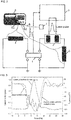
- FIG. 2 is a schematic structural view of an apparatus for implementing the method shown in FIG. 1 .
- a controllable splitting method for a high current pulse includes the following steps:
- the peak current of the current pulse ranges from 10 amps to 10000 amps, and the pulse width in the time domain of the current pulse ranges from 0.01 ns to 1000 ns.
- the silicon carbide substrate of the planar silicon carbide photoconductive switch described above may be high-purity semi-insulating silicon carbide, vanadium-doped semi-insulating silicon carbide, or unintentionally doped semi-insulating silicon carbide.
- the number of split peaks in the output current pulse signal having a split waveform is from 2 to 10.
- the pulse laser has a wavelength ranging from 100 nm to 1064 nm, and the laser pulse has an intensity ranging from 5 ⁇ J/mm 2 to 5000 ⁇ J/mm 2 .
- an apparatus for implementing a controllable splitting method for a high current pulse includes: a pulse laser, a planar silicon carbide photoconductive switch, an optical path, and a connection cable.
- the optical path may be connected in the form of a group of optical paths or only optical fibers.
- the pulse width in the time domain of the output pulse from the pulse laser may range from 0.01 nanoseconds to 1000 nanoseconds.
- the planar silicon carbide photoconductive switch may be a planar gallium nitride photoconductive switch, a planar diamond photoconductive switch, a planar gallium arsenide photoconductive switch, or a planar indium phosphide photoconductive switch.
- the present application provides a method and an apparatus for controllable splitting of a high current pulse with the following beneficial technical effects:
- the entire apparatus only has two main components-a pulse laser and a silicon carbide photoconductive switch-which makes the apparatus overall simple, easy to control, and high in stability.
- a controllable splitting method and apparatus for a high current pulse of the present application includes a pulse laser 3, a planar silicon carbide photoconductive switch 2, an optical path, and a connection cable 8.
- the following examples implement the method and apparatus of the present application by using the circuit connection manner shown in FIG. 2 , and specifically the following steps are performed.
- Example 1 a photoconductive switch 2 having an electrode spacing of 5 mm is utilized, which is prepared using a vanadium-doped silicon carbide substrate, and a single-pulse laser intensity is 150 ⁇ J/mm 2 .
- FIG. 3 is a graph showing the results of the splitting of a high current pulse according to the method of Example 1 of the present application, and the output current pulse from the apparatus of the present application when the input peak current is 130 amps is shown. It can be seen that the output current pulse is split regularly into 5 peaks with peak values between 100 amps and 130 amps.
- the method and apparatus of the present application are implemented using the circuit connection shown in FIG. 2 , specifically according to the following steps.
- Example 2 a photo-conductive switch having an electrode spacing of 10 mm is utilized, which is prepared using an unintentionally doped silicon carbide substrate, and the single-pulse laser light has an intensity of 350 ⁇ J/mm 2 .
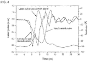
- FIG. 4 is a graph showing the results of the splitting of a high current pulse according to the method of Example 2 of the present application, and the output current pulse from the apparatus of the present application when the input peak current is 90 ampere is shown. It can be seen that the output current pulse is split regularly into 2 peaks whose peak values are between 90 amps and 100 amps, and which are close to each other.
Landscapes
- Physics & Mathematics (AREA)
- Nonlinear Science (AREA)
- Lasers (AREA)
- Semiconductor Lasers (AREA)
Description
- The present application belongs to the field of pulse power technology, and in particular, relates to a controllable splitting method for a high current pulse and an apparatus therefor.
- Pulse power technology involves many defense and cutting-edge technology fields such as high-power radars, large-scale accelerators, high-power pulsed power supplies, etc. The core of pulse power technology is the precise control of high current pulses on the time domain and amplitude, so as to achieve accurate operation of radars, accelerators, and other devices. Therefore, it is important to study the control of the current pulse waveform in the pulse power field.
- The control of the current pulse waveform includes the compression of the pulse width, the splitting of a single pulse, and the like, to meet the operational requirements of the pulse power systems. The traditional method uses electrical components to achieve this. However, currently the relevant electrical components are mostly made of semiconductor silicon materials, the performance of the components is limited by the physical properties of the silicon material itself, and thus its ability to withstand high voltage and high current is very limited. Therefore, in the operating conditions of a magnitude of tens to hundreds of kilovolts and kiloamperes which are common in the field of pulse power technology, a large number of components are required to realize the regulation of the current pulse waveform, resulting in a large volume and a high power loss.
- As the preparation technology of wide bandgap semiconductor materials is getting increasingly mature, people have turned their attention to using wide bandgap semiconductor materials for high-power photoconductive switches. Silicon carbide, as a representative of wide bandgap semiconductors, has more prominent advantages than other wide bandgap semiconductor materials-that is, a high critical breakdown field strength and a high thermal conductivity, which were absent in the conventional semiconductor materials such as silicon. According to the characteristics of silicon carbide materials, a number of silicon carbide photoconductive switches have been proposed in recent years. The on and off states of such switches are controlled by a laser signal, which is very simple and accurate. At the same time, because of the excellent physical properties of silicon carbide materials, a single silicon carbide switch can withstand high-power operating environments of a magnitude of tens to hundreds of kilovolts and kiloamperes. Such a switch is the ideal switch that is expected in the field of pulse power, which switch will make the pulse power system be greatly simplified, has a reduced size, a lower cost, and improved stability, and thus is of great significance to the defense technology and other fields.
-
WO 2007/149846 A2 discloses an arrangement of a plurality of transistors and tyristors, giving a near square wave output with a width of several hundred nano seconds. -
US 5,278,854 A discloses the use of gallium arsenite to amplify a low power signal of a microwave frequency input. -
WO 2009/129512 A2 discloses the use of photoconductive semi-conductors and a variable resistance element and produces a modulated light signal via a modulation module. - In view of the above problems in the prior art, the technical problem to be solved by the present application is to provide a controllable splitting method for a high current pulse and an apparatus therefor, which have the advantages of being compact, small in size, and simple with regard to control system compared with conventional methods and apparatuses.
- In order to solve the above technical problems, the invention is defined by a method in accordance with claim 1 and an apparatus implementing said method in accordance with
claim 7. Accordingly, in one aspect, the present invention provides a controllable splitting method for a high current pulse, including among other: - (1) Electrically connecting a silicon carbide photoconductive switch between an input end and an output end of a current pulse;
- (2) Connecting a time-domain signal of an input current pulse to an external triggering port of a pulse laser;
- (3) Irradiating a laser pulse emitted by the pulse laser to the silicon carbide photoconductive switch;
- (4) When no current pulse is input at the input end, the pulse laser failing to receive an external trigger signal, and to output the laser pulse, the silicon carbide photoconductive switch being in an off state without the irradiation of the laser pulse, and no current being output from the output end;
- (5) When a current pulse is input at the input end, a time-domain signal triggering the pulse laser so that the pulse laser synchronously outputs a laser pulse on the time domain, the laser pulse irradiating the silicon carbide photoconductive switch so that the silicon carbide photoconductive switch is in an on state and a current pulse is output from the output end;
- (6) Controlling the waveform of the current pulse by the parameters of the photoconductive switch so that a current pulse signal having a split waveform is formed at the output end in synchronization with the time domain of the input end.
- According to the present application, the controllable splitting method of a high current pulse can split the time-domain signal of the Gaussian-like distributed current pulse, which is currently common in the pulsed power system, so that a single current pulse peak can be split into multiple current pulse peaks with narrower widths.
- A photoconductive switch is directly connected to the input and output of a high current pulse. The photoconductive switch is in an off state when there is no laser excitation, and the entire apparatus has no output. When there is a high current pulse input, the time-domain signal serves as an external trigger source for the pulse laser, so that the pulse laser synchronously outputs a laser pulse. This laser pulse excites the photoconductive switch so that the photoconductive switch turns into an on state within a duration of a laser pulse, and thus a current pulse is output at the output end. Because of the special physical properties of the photoconductive switch, the output current pulse varies according to the parameters such as the excitation light intensity, the electrode spacing, etc., thereby realizing regulation of the splitting waveform of the output current pulse.
- In addition, according to the invention, the photoconductive switch is a planar silicon carbide photoconductive switch whose silicon carbide substrate is high-purity semi-insulating silicon carbide, vanadium-doped semi-insulating silicon carbide, or unintentionally doped semi-insulating silicon carbide.
- According to the present application, the function of realizing the splitting of a high current peak is mainly determined by the special physical properties of the planar silicon carbide photoconductive switch under light excitation. Because of the special physical properties of the planar silicon carbide photo-conductive switch, the output current pulse varies according to the parameters such as the excitation light intensity, the planar silicon carbide electrode spacing, etc., which is beneficial to realize the regulation of the splitting waveform of the output current pulse. High-purity semi-insulating silicon carbide, vanadium-doped semi-insulating silicon carbide, or unintentionally doped semi-insulating silicon carbide will produce carriers with different generation and trapping effects due to the difference in the impurity levels, and thus different split waveforms are shown in the output current pulse peaks.
- In addition, according to the invention, the number of split peaks in the output current pulse signal having a split waveform is from 2 to 10.
- According to the present application, in the case of the same input current value, the output current pulse generates different numbers of split peaks, and individual current peaks of different current values can be generated, so that output current pulses of different current values can be obtained by adjusting the number of split peaks.
- In addition, in the present application, it is also possible that the laser pulse output from the pulse laser has a wavelength ranging from 100 nm to 1064 nm.
- According to the present application, excitation laser pulses with different wavelengths can excite carriers at different impurity levels, and therefore, the different wavelengths of excitation laser pulses can adjust the magnitude of the output pulse current.
- In addition, in the present application, it is also possible that the intensity of the laser pulse output from the pulse laser is in the range from 5 µJ/mm2 to 5000 µJ/mm2.
- According to the present application, by adjusting the intensity of the excitation laser pulse, different concentrations of photocarriers can be obtained, so that the output current values can be effectively adjusted, and the number of split peaks can also be adjusted.
- In another aspect, the present application also provides an apparatus for implementing the controllable splitting method for a high current pulse as described above, comprising: a silicon carbide photoconductive switch electrically connected between an input end and an output end of a current pulse; and a pulse laser receiving a time-domain signal of an input current pulse, a laser pulse emitted by the pulse laser being irradiated to the silicon carbide photoconductive switch.
- According to the present application, a time-domain signal of a Gaussian-like distributed current pulse, which is common in current pulsed power systems, can be split by the apparatus so that a single current pulse peak is split into a plurality of current pulse peaks having narrower widths.
- In addition, in the present application, the pulse width in the time domain of an output pulse from the pulse laser may be in the range from 0.01 nanoseconds to 1000 nanoseconds.
- According to the present application, by adjusting the pulse width in the time domain of the output pulse of the pulse laser, the overall pulse width of the output current peak can be simultaneously regulated.
- The foregoing and other objects, features, and advantages of the present application will be better understood from the following detailed description and with reference to the drawings.
-
-
FIG 1 is a schematic diagram of a controllable splitting method for a high current pulse according to an embodiment of the present application; -
FIG 2 is a schematic structural view of an apparatus for implementing the method shown inFIG. 1 ; -
FIG 3 is a graph illustrating the result of splitting a high current pulse according to the method of the first example of the present application; -
FIG. 4 is a graph illustrating the result of splitting a high current pulse according to the method of the second example of the present application. - 1 - pulse high-voltage source; 11 - input end; 12 - output end; 2 - silicon carbide photoconductive switch; 3 - pulse laser; 4 - first high-voltage withstanding precision resistor; 5 - second high-voltage withstanding precision resistor; 6 - oscilloscope; 61, 62 - probe; 7 - photocell; 8 - cable.
- Hereinafter, the apparatus and the method of the present application will be described in detail with reference to the accompanying drawings.
- In view of the existing defects in the control of current pulse waveform in the technology field of pulse power, the present application provides a novel and simple controllable method and apparatus for splitting high current pulses utilizing a silicon carbide photoconductive switch which is a new high-performance switching device, as well as utilizing the physical phenomenon that the silicon carbide photoconductive switch can regulate the waveform of a current pulse flowing through it, which is discovered by the inventor in the research for the first time. The method and the apparatus have important potential application value in the field of pulse power technology, and have great significance in defense and frontier science and technology and other fields.
-
FIG. 1 is a schematic diagram of a controllable splitting method for a high current pulse according to an embodiment of the present application, andFIG. 2 is a schematic structural view of an apparatus for implementing the method shown inFIG. 1 . - As shown in
FIG. 1 andFIG. 2 , a controllable splitting method for a high current pulse according to the present application includes the following steps: - 1) Electrically connecting a silicon carbide photoconductive switch between an input end and an output end of a current pulse, wherein the silicon carbide photoconductive switch may be a planar silicon carbide photoconductive switch;
- 2) Connecting a time-domain signal of an input current pulse to an external triggering port of a pulse laser;
- 3) Irradiating a laser pulse emitted by the pulse laser to the planar silicon carbide photoconductive switch;
- 4) When no current pulse is input at the input end, the pulse laser failing to receive the external trigger signal, and to output the laser pulse, the silicon carbide photoconductive switch being in an off state without laser pulse irradiation, and no current being output from the output end;
- 5) When a current pulse is input at the input end, a time-domain signal triggering the pulse laser, so that the pulse laser synchronously outputs a laser pulse on the time domain, the laser pulse irradiating the silicon carbide photoconductive switch so that the silicon carbide photoconductive switch is in an on state and a current pulse is output from the output end; and
- 6) The current flowing through the planar silicon carbide photoconductive switch, and the waveform of the current pulse being controlled by the relevant parameters of the photoconductive switch, so that a current pulse signal having certain split waveform is formed at the output end in synchronization with the time domain of the input end.
- In the above steps, it is preferable that the peak current of the current pulse ranges from 10 amps to 10000 amps, and the pulse width in the time domain of the current pulse ranges from 0.01 ns to 1000 ns.
- In addition, the silicon carbide substrate of the planar silicon carbide photoconductive switch described above may be high-purity semi-insulating silicon carbide, vanadium-doped semi-insulating silicon carbide, or unintentionally doped semi-insulating silicon carbide.
- In addition, in the above method, the number of split peaks in the output current pulse signal having a split waveform is from 2 to 10.
- Also, in the above steps, it is preferable that the pulse laser has a wavelength ranging from 100 nm to 1064 nm, and the laser pulse has an intensity ranging from 5 µJ/mm2 to 5000 µJ/mm2.
- On the other aspect, an apparatus for implementing a controllable splitting method for a high current pulse according to an embodiment of the present application includes: a pulse laser, a planar silicon carbide photoconductive switch, an optical path, and a connection cable. Preferably, the optical path may be connected in the form of a group of optical paths or only optical fibers. Also, the pulse width in the time domain of the output pulse from the pulse laser may range from 0.01 nanoseconds to 1000 nanoseconds.
- In addition, more preferably, the planar silicon carbide photoconductive switch may be a planar gallium nitride photoconductive switch, a planar diamond photoconductive switch, a planar gallium arsenide photoconductive switch, or a planar indium phosphide photoconductive switch.
- Compared with the current method of controlling the waveform of a current pulse simply by electrical elements in the field of pulse power technology, the present application provides a method and an apparatus for controllable splitting of a high current pulse with the following beneficial technical effects: In addition to the optical path connection and electrical connection, the entire apparatus only has two main components-a pulse laser and a silicon carbide photoconductive switch-which makes the apparatus overall simple, easy to control, and high in stability.
- The preferred examples of the present application will be further described in detail below with reference to the accompanying drawings.
- In the embodiment shown in
FIG. 1 , a controllable splitting method and apparatus for a high current pulse of the present application includes apulse laser 3, a planar siliconcarbide photoconductive switch 2, an optical path, and aconnection cable 8. The following examples implement the method and apparatus of the present application by using the circuit connection manner shown inFIG. 2 , and specifically the following steps are performed. - 1) A pulse high-voltage source 1 is used as the input of the high current pulse, and its positive electrode is electrically connected to the positive electrode of the
photoconductive switch 2 and to the positive electrode of a first high-voltage withstanding precision resistor 4 on the left. The time-domain signal of the pulse high-voltage source 1 is electrically connected to the external triggering port of thepulse laser 3. - 2) The negative electrode of the pulse high-
voltage source 3 and the negative electrodes of the two high-voltage withstandingprecision resistors 4 and 5 are connected electrically to the ground. - 3) The negative electrode of the
photoconductive switch 2 is connected electrically to the positive electrode of the second high-voltage withstandingprecision resistor 5 on the right. - 4) A laser spot emitted from the
pulse laser 3 is irradiated to the planar siliconcarbide photoconductive switch 2 by means of a set of reflecting mirrors (not shown). - 5) A
photocell 7 is used to receive the scattered light of the laser, and output the laser pulse signal to theoscilloscope 6. - 6) The
oscilloscope 6 collects the voltage signals at the two ends of the two high-voltage precision resistors 4, 5 through twoprobes oscilloscope 6. - In Example 1, a
photoconductive switch 2 having an electrode spacing of 5 mm is utilized, which is prepared using a vanadium-doped silicon carbide substrate, and a single-pulse laser intensity is 150 µJ/mm2.FIG. 3 is a graph showing the results of the splitting of a high current pulse according to the method of Example 1 of the present application, and the output current pulse from the apparatus of the present application when the input peak current is 130 amps is shown. It can be seen that the output current pulse is split regularly into 5 peaks with peak values between 100 amps and 130 amps. - The method and apparatus of the present application are implemented using the circuit connection shown in
FIG. 2 , specifically according to the following steps. - 1) A pulse high-voltage source 1 is used as the input of the high current pulse, and its positive electrode is electrically connected to the positive electrode of the
photoconductive switch 2 and to the positive electrode of a first high-voltage withstanding precision resistor 4 on the left. The time-domain signal of the pulse high-voltage source 1 is electrically connected to the external triggering port of thepulse laser 3. - 2) The negative electrode of the pulse high-
voltage source 3 and the negative electrodes of the two high-voltage withstandingprecision resistors 4 and 5 are connected electrically to the ground. - 3) The negative electrode of the
photoconductive switch 2 is connected electrically to the positive electrode of the second high-voltage withstandingprecision resistor 5 on the right. - 4) A laser spot emitted from the
pulse laser 3 is irradiated to the planar siliconcarbide photoconductive switch 2 by means of a set of reflecting mirrors (not shown). - 5) A
photocell 7 is used to receive the scattered light of the laser and output the laser pulse signal to theoscilloscope 6. - 6) The
oscilloscope 6 collects the voltage signals at the two ends of the two high-voltage precision resistors 4, 5 through twoprobes oscilloscope 6. - In Example 2, a photo-conductive switch having an electrode spacing of 10 mm is utilized, which is prepared using an unintentionally doped silicon carbide substrate, and the single-pulse laser light has an intensity of 350 µJ/mm2.
FIG. 4 is a graph showing the results of the splitting of a high current pulse according to the method of Example 2 of the present application, and the output current pulse from the apparatus of the present application when the input peak current is 90 ampere is shown. It can be seen that the output current pulse is split regularly into 2 peaks whose peak values are between 90 amps and 100 amps, and which are close to each other. - The invention can be embodied in many forms and the embodiments of the application are intended to be illustrative and not restrictive. The scope of the invention is defined by the claims rather than the specification
Claims (9)
- A controllable splitting method for a high current pulse, characterized in that the method comprises steps of:(1) electrically connecting one silicon carbide photoconductive switch (2) between an input end (11) and an output end (12) of a current pulse circuit for the current pulse;(2) a pulse high-voltage source (1) is used as an input of the current pulse, a time-domain signal of the pulse high-voltage source (1) is electrically connected to an external triggering port of a pulse laser (3) to serve as an external trigger signal;(3) irradiating a laser pulse emitted by the pulse laser (3) to the silicon carbide photoconductive switch (2);(4) when no current pulse is input at the input end (11), the pulse laser (3) failing to receive the external trigger signal, and to output the laser pulse, the silicon carbide photoconductive switch (2) being in an off state without the irradiation of the laser pulse (3), and no current being output from the output end (12);(5) when the current pulse is input at the input end (11), the time-domain signal triggering the pulse laser (3) so that the pulse laser (3) synchronously outputs a laser pulse on a time domain, the laser pulse irradiating the silicon carbide photoconductive switch (2) so that the silicon carbide photoconductive switch (2) is in an on state and an output current pulse with an output current pulse signal is output from the output end (12);(6) controlling the waveform of the output current pulse by parameters including the excitation light intensity and the silicon carbide electrode spacing of the silicon carbide photoconductive switch (2), the output current pulse signal varies according to the parameters, so that a current pulse signal having a split waveform is formed at the output end (12) in synchronization with the time domain of the input end (11), wherein the number of split peaks in the output current pulse signal having a split waveform is from 2 to 10.
- The controllable splitting method for the high current pulse according to claim 1, wherein a peak current of the current pulse ranges from 10 amps to 10000 amps.
- The controllable splitting method for the high current pulse according to claim 1, wherein a pulse width of the time domain of the current pulse ranges from 0.01 ns to 1000 ns.
- The controllable splitting method for the high current pulse according to claim 1, wherein the silicon carbide photoconductive switch (2) is a planar silicon carbide photoconductive switch, and a silicon carbide substrate thereof is high-purity semi-insulating silicon carbide, or vanadium-doped semi-insulating silicon carbide.
- The controllable splitting method for the high current pulse according to claim 1, wherein the laser pulse output from the pulse laser (3) has a wavelength ranging from 100 nm to 1064 nm.
- The controllable splitting method for the high current pulse according to claim 1, wherein the laser pulse output from the pulse laser (3) has an intensity ranging from 5 µJ/mm2 to 5000 µJ/mm2.
- An apparatus for implementing the controllable splitting method for the high current pulse according to any one of claims 1 to 6, characterized in that the apparatus comprises:the silicon carbide photoconductive switch (2) electrically connected between the input end (11) and the output end (12) of the current pulse circuit for the current pulse;the pulse high-voltage source (1) used as an input of the current pulse, its positive electrode is electrically connected to the positive electrode of the silicon carbide photoconductive switch (2), the time-domain signal of the pulse high-voltage source (1) is electrically connected to the external triggering port of the pulse laser (3); andthe pulse laser (3) receiving the time-domain signal of the pulse high-voltage source (1), a laser pulse emitted by the pulse laser (3) being irradiated to the silicon carbide photoconductive switch (2).
- The apparatus for implementing the controllable splitting method for the high current pulse according to claim 7, wherein the pulse width in the time domain of an output pulse from the pulse laser (3) is in the range from 0.01 nanoseconds to 1000 nanoseconds.
- The apparatus for implementing the controllable splitting method for the high current pulse according to claim 7 or 8, wherein the silicon carbide photoconductive switch (2) is a planar silicon carbide photoconductive switch.
Applications Claiming Priority (2)
| Application Number | Priority Date | Filing Date | Title |
|---|---|---|---|
| CN201510948411.8A CN105450209B (en) | 2015-12-17 | 2015-12-17 | A kind of the controlled cleaving method and its device of heavy current pulse |
| PCT/CN2015/100259 WO2017101167A1 (en) | 2015-12-17 | 2015-12-31 | Controllable splitting method for large current pulse and apparatus therefor |
Publications (3)
| Publication Number | Publication Date |
|---|---|
| EP3393041A1 EP3393041A1 (en) | 2018-10-24 |
| EP3393041A4 EP3393041A4 (en) | 2019-08-14 |
| EP3393041B1 true EP3393041B1 (en) | 2020-11-11 |
Family
ID=55560070
Family Applications (1)
| Application Number | Title | Priority Date | Filing Date |
|---|---|---|---|
| EP15910636.8A Active EP3393041B1 (en) | 2015-12-17 | 2015-12-31 | Controllable splitting method for large current pulse and apparatus therefor |
Country Status (4)
| Country | Link |
|---|---|
| US (1) | US10651833B2 (en) |
| EP (1) | EP3393041B1 (en) |
| CN (1) | CN105450209B (en) |
| WO (1) | WO2017101167A1 (en) |
Families Citing this family (2)
| Publication number | Priority date | Publication date | Assignee | Title |
|---|---|---|---|---|
| US20220165905A1 (en) * | 2020-11-20 | 2022-05-26 | The Board Of Trustees Of The Leland Stanford Junior University | Devices and methods involving diamond-based photoconductive structures |
| CN119087205B (en) * | 2024-09-19 | 2025-11-25 | 中国科学院苏州纳米技术与纳米仿生研究所 | Photoconductive switch testing system and testing method |
Family Cites Families (12)
| Publication number | Priority date | Publication date | Assignee | Title |
|---|---|---|---|---|
| US5278854A (en) * | 1992-09-18 | 1994-01-11 | The United States Of America As Represented By The Secretary Of The Army | Signal amplification using optically activated bulk semi-insulating GaAs |
| USH1717H (en) * | 1995-11-16 | 1998-04-07 | The United States Of America As Represented By The Secretary Of The Navy | Bistable photoconductive switches particularly suited for frequency-agile, radio-frequency sources |
| US5804815A (en) | 1996-07-05 | 1998-09-08 | Sandia Corporation | GaAs photoconductive semiconductor switch |
| US5811841A (en) * | 1997-04-03 | 1998-09-22 | The United States Of America As Represented By The Secretary Of The Air Force | Photoconductive switching with thin layer enhanced breakdown charateristics |
| CN100375345C (en) * | 2004-12-31 | 2008-03-12 | 中国科学院西安光学精密机械研究所 | cavity emptying laser |
| US8193537B2 (en) * | 2006-06-19 | 2012-06-05 | Ss Sc Ip, Llc | Optically controlled silicon carbide and related wide-bandgap transistors and thyristors |
| CN102047443B (en) * | 2008-04-17 | 2014-07-09 | 劳伦斯利弗莫尔国家安全有限责任公司 | Systems and methods for modulating electrical signals using photoconductive wide bandgap semiconductors as variable resistors |
| CN100553130C (en) * | 2008-05-16 | 2009-10-21 | 西安理工大学 | Ultrafast pulse power switching device and self-excited picosecond power pulse generator |
| JP5148381B2 (en) * | 2008-06-18 | 2013-02-20 | 株式会社アドバンテスト | Light measuring device |
| US9240506B2 (en) * | 2009-12-08 | 2016-01-19 | Lawrence Livermore National Security, Llc | Transparent ceramic photo-optical semiconductor high power switches |
| CN102157597A (en) * | 2010-02-11 | 2011-08-17 | 中国科学院上海硅酸盐研究所 | Optical control silicon carbide (SiC) photoconductive switch |
| WO2013114351A2 (en) * | 2012-01-31 | 2013-08-08 | HIL Applied Medical Ltd. | Laser activated magnetic field manipulation of laser driven ion beams |
-
2015
- 2015-12-17 CN CN201510948411.8A patent/CN105450209B/en active Active
- 2015-12-31 WO PCT/CN2015/100259 patent/WO2017101167A1/en not_active Ceased
- 2015-12-31 US US16/062,777 patent/US10651833B2/en active Active
- 2015-12-31 EP EP15910636.8A patent/EP3393041B1/en active Active
Non-Patent Citations (1)
| Title |
|---|
| None * |
Also Published As
| Publication number | Publication date |
|---|---|
| US20190296721A1 (en) | 2019-09-26 |
| EP3393041A4 (en) | 2019-08-14 |
| WO2017101167A1 (en) | 2017-06-22 |
| EP3393041A1 (en) | 2018-10-24 |
| CN105450209A (en) | 2016-03-30 |
| US10651833B2 (en) | 2020-05-12 |
| CN105450209B (en) | 2018-10-30 |
Similar Documents
| Publication | Publication Date | Title |
|---|---|---|
| CN101795127B (en) | High-voltage square-wave pulse generator and method for generating high-voltage square-wave pulse | |
| Leach et al. | High voltage bulk GaN-based photoconductive switches for pulsed power applications | |
| CN101132114A (en) | Continuously adjustable nanosecond pulse semiconductor laser drive power supply | |
| US5864166A (en) | Bistable photoconductive switches particularly suited for frequency-agile, radio-frequency sources | |
| US9893679B2 (en) | High frequency modulation circuits based on photoconductive wide bandgap switches | |
| US10651833B2 (en) | Controllable splitting method for high current pulse and apparatus therefor | |
| Ramezani et al. | Solid-state high-voltage pulse generator for low temperature plasma ion mobility spectrometry | |
| CN108075749B (en) | High voltage light-controlled pulse thyristor and its trigger control system and trigger control method | |
| Wang et al. | Analysis of the on-state resistance of photoconductive semiconductor switches in the non-linear mode | |
| CN103094833A (en) | Pulse drive circuit of semiconductor laser based on avalanche transistor | |
| Li et al. | Ultrafast characteristics of integrated high-power photoconductive semiconductor switch based on 4H-SiC substrate | |
| El Amari et al. | Characterization of a linear photoconductive switch used in nanosecond pulsed electric field generator | |
| CN207801884U (en) | A kind of photo thyristor and its Triggering Control System | |
| CN203242917U (en) | A pulse semiconductor laser device driving circuit based on an avalanche transistor | |
| Wu et al. | Study on output characteristics of 20 kV/100 ns nonlinear GaAs photoconductive semiconductor switch | |
| Shi et al. | Comparison on the synchronization of two parallel GaAs photoconductive semiconductor switches excited by laser diodes | |
| Cronson | Picosecond-Pulse Sequential Waveform Generation (Short Papers) | |
| CN204376192U (en) | A kind of pulsed laser energy stabilizing arrangement | |
| Mauch et al. | Evaluation of a pulsed ultraviolet light-emitting diode for triggering photoconductive semiconductor switches | |
| Barmin et al. | Effect on the GaAs parameters of a photoconductive semiconductor switch with a silicon oxide layer when switched by 355-nm laser radiation | |
| Vergne et al. | High-voltage rectifier diodes used as photoconductive device for microwave pulse generation | |
| Ma et al. | High Current Operation of a Semi-Insulating Gallium Arsenide Photoconductive Semiconductor Switch Triggered by the Light Produced by a Spark Gap | |
| Ren et al. | LED-triggered photoconductive semiconductor switches for nanosecond pulse generation | |
| Zajc et al. | Expanding the power pulse duration range for electroporation | |
| Williams et al. | Biasing Josephson junctions with optoelectronically generated pulses |
Legal Events
| Date | Code | Title | Description |
|---|---|---|---|
| STAA | Information on the status of an ep patent application or granted ep patent |
Free format text: STATUS: THE INTERNATIONAL PUBLICATION HAS BEEN MADE |
|
| PUAI | Public reference made under article 153(3) epc to a published international application that has entered the european phase |
Free format text: ORIGINAL CODE: 0009012 |
|
| STAA | Information on the status of an ep patent application or granted ep patent |
Free format text: STATUS: REQUEST FOR EXAMINATION WAS MADE |
|
| 17P | Request for examination filed |
Effective date: 20180710 |
|
| AK | Designated contracting states |
Kind code of ref document: A1 Designated state(s): AL AT BE BG CH CY CZ DE DK EE ES FI FR GB GR HR HU IE IS IT LI LT LU LV MC MK MT NL NO PL PT RO RS SE SI SK SM TR |
|
| AX | Request for extension of the european patent |
Extension state: BA ME |
|
| DAV | Request for validation of the european patent (deleted) | ||
| DAX | Request for extension of the european patent (deleted) | ||
| A4 | Supplementary search report drawn up and despatched |
Effective date: 20190716 |
|
| RIC1 | Information provided on ipc code assigned before grant |
Ipc: H03K 17/78 20060101ALI20190710BHEP Ipc: H03K 5/04 20060101AFI20190710BHEP |
|
| GRAP | Despatch of communication of intention to grant a patent |
Free format text: ORIGINAL CODE: EPIDOSNIGR1 |
|
| STAA | Information on the status of an ep patent application or granted ep patent |
Free format text: STATUS: GRANT OF PATENT IS INTENDED |
|
| INTG | Intention to grant announced |
Effective date: 20200717 |
|
| GRAS | Grant fee paid |
Free format text: ORIGINAL CODE: EPIDOSNIGR3 |
|
| GRAA | (expected) grant |
Free format text: ORIGINAL CODE: 0009210 |
|
| STAA | Information on the status of an ep patent application or granted ep patent |
Free format text: STATUS: THE PATENT HAS BEEN GRANTED |
|
| AK | Designated contracting states |
Kind code of ref document: B1 Designated state(s): AL AT BE BG CH CY CZ DE DK EE ES FI FR GB GR HR HU IE IS IT LI LT LU LV MC MK MT NL NO PL PT RO RS SE SI SK SM TR |
|
| REG | Reference to a national code |
Ref country code: GB Ref legal event code: FG4D |
|
| REG | Reference to a national code |
Ref country code: CH Ref legal event code: EP |
|
| REG | Reference to a national code |
Ref country code: AT Ref legal event code: REF Ref document number: 1334432 Country of ref document: AT Kind code of ref document: T Effective date: 20201115 |
|
| REG | Reference to a national code |
Ref country code: DE Ref legal event code: R096 Ref document number: 602015062034 Country of ref document: DE |
|
| REG | Reference to a national code |
Ref country code: IE Ref legal event code: FG4D |
|
| REG | Reference to a national code |
Ref country code: NL Ref legal event code: MP Effective date: 20201111 |
|
| REG | Reference to a national code |
Ref country code: AT Ref legal event code: MK05 Ref document number: 1334432 Country of ref document: AT Kind code of ref document: T Effective date: 20201111 |
|
| PG25 | Lapsed in a contracting state [announced via postgrant information from national office to epo] |
Ref country code: FI Free format text: LAPSE BECAUSE OF FAILURE TO SUBMIT A TRANSLATION OF THE DESCRIPTION OR TO PAY THE FEE WITHIN THE PRESCRIBED TIME-LIMIT Effective date: 20201111 Ref country code: RS Free format text: LAPSE BECAUSE OF FAILURE TO SUBMIT A TRANSLATION OF THE DESCRIPTION OR TO PAY THE FEE WITHIN THE PRESCRIBED TIME-LIMIT Effective date: 20201111 Ref country code: PT Free format text: LAPSE BECAUSE OF FAILURE TO SUBMIT A TRANSLATION OF THE DESCRIPTION OR TO PAY THE FEE WITHIN THE PRESCRIBED TIME-LIMIT Effective date: 20210311 Ref country code: NO Free format text: LAPSE BECAUSE OF FAILURE TO SUBMIT A TRANSLATION OF THE DESCRIPTION OR TO PAY THE FEE WITHIN THE PRESCRIBED TIME-LIMIT Effective date: 20210211 Ref country code: GR Free format text: LAPSE BECAUSE OF FAILURE TO SUBMIT A TRANSLATION OF THE DESCRIPTION OR TO PAY THE FEE WITHIN THE PRESCRIBED TIME-LIMIT Effective date: 20210212 |
|
| PG25 | Lapsed in a contracting state [announced via postgrant information from national office to epo] |
Ref country code: AT Free format text: LAPSE BECAUSE OF FAILURE TO SUBMIT A TRANSLATION OF THE DESCRIPTION OR TO PAY THE FEE WITHIN THE PRESCRIBED TIME-LIMIT Effective date: 20201111 Ref country code: BG Free format text: LAPSE BECAUSE OF FAILURE TO SUBMIT A TRANSLATION OF THE DESCRIPTION OR TO PAY THE FEE WITHIN THE PRESCRIBED TIME-LIMIT Effective date: 20210211 Ref country code: IS Free format text: LAPSE BECAUSE OF FAILURE TO SUBMIT A TRANSLATION OF THE DESCRIPTION OR TO PAY THE FEE WITHIN THE PRESCRIBED TIME-LIMIT Effective date: 20210311 Ref country code: LV Free format text: LAPSE BECAUSE OF FAILURE TO SUBMIT A TRANSLATION OF THE DESCRIPTION OR TO PAY THE FEE WITHIN THE PRESCRIBED TIME-LIMIT Effective date: 20201111 Ref country code: SE Free format text: LAPSE BECAUSE OF FAILURE TO SUBMIT A TRANSLATION OF THE DESCRIPTION OR TO PAY THE FEE WITHIN THE PRESCRIBED TIME-LIMIT Effective date: 20201111 Ref country code: PL Free format text: LAPSE BECAUSE OF FAILURE TO SUBMIT A TRANSLATION OF THE DESCRIPTION OR TO PAY THE FEE WITHIN THE PRESCRIBED TIME-LIMIT Effective date: 20201111 |
|
| REG | Reference to a national code |
Ref country code: LT Ref legal event code: MG9D |
|
| PG25 | Lapsed in a contracting state [announced via postgrant information from national office to epo] |
Ref country code: HR Free format text: LAPSE BECAUSE OF FAILURE TO SUBMIT A TRANSLATION OF THE DESCRIPTION OR TO PAY THE FEE WITHIN THE PRESCRIBED TIME-LIMIT Effective date: 20201111 |
|
| REG | Reference to a national code |
Ref country code: DE Ref legal event code: R119 Ref document number: 602015062034 Country of ref document: DE |
|
| PG25 | Lapsed in a contracting state [announced via postgrant information from national office to epo] |
Ref country code: LT Free format text: LAPSE BECAUSE OF FAILURE TO SUBMIT A TRANSLATION OF THE DESCRIPTION OR TO PAY THE FEE WITHIN THE PRESCRIBED TIME-LIMIT Effective date: 20201111 Ref country code: SM Free format text: LAPSE BECAUSE OF FAILURE TO SUBMIT A TRANSLATION OF THE DESCRIPTION OR TO PAY THE FEE WITHIN THE PRESCRIBED TIME-LIMIT Effective date: 20201111 Ref country code: CZ Free format text: LAPSE BECAUSE OF FAILURE TO SUBMIT A TRANSLATION OF THE DESCRIPTION OR TO PAY THE FEE WITHIN THE PRESCRIBED TIME-LIMIT Effective date: 20201111 Ref country code: EE Free format text: LAPSE BECAUSE OF FAILURE TO SUBMIT A TRANSLATION OF THE DESCRIPTION OR TO PAY THE FEE WITHIN THE PRESCRIBED TIME-LIMIT Effective date: 20201111 Ref country code: SK Free format text: LAPSE BECAUSE OF FAILURE TO SUBMIT A TRANSLATION OF THE DESCRIPTION OR TO PAY THE FEE WITHIN THE PRESCRIBED TIME-LIMIT Effective date: 20201111 Ref country code: RO Free format text: LAPSE BECAUSE OF FAILURE TO SUBMIT A TRANSLATION OF THE DESCRIPTION OR TO PAY THE FEE WITHIN THE PRESCRIBED TIME-LIMIT Effective date: 20201111 |
|
| REG | Reference to a national code |
Ref country code: CH Ref legal event code: PL |
|
| PG25 | Lapsed in a contracting state [announced via postgrant information from national office to epo] |
Ref country code: MC Free format text: LAPSE BECAUSE OF FAILURE TO SUBMIT A TRANSLATION OF THE DESCRIPTION OR TO PAY THE FEE WITHIN THE PRESCRIBED TIME-LIMIT Effective date: 20201111 Ref country code: DK Free format text: LAPSE BECAUSE OF FAILURE TO SUBMIT A TRANSLATION OF THE DESCRIPTION OR TO PAY THE FEE WITHIN THE PRESCRIBED TIME-LIMIT Effective date: 20201111 |
|
| REG | Reference to a national code |
Ref country code: BE Ref legal event code: MM Effective date: 20201231 |
|
| PLBE | No opposition filed within time limit |
Free format text: ORIGINAL CODE: 0009261 |
|
| STAA | Information on the status of an ep patent application or granted ep patent |
Free format text: STATUS: NO OPPOSITION FILED WITHIN TIME LIMIT |
|
| 26N | No opposition filed |
Effective date: 20210812 |
|
| GBPC | Gb: european patent ceased through non-payment of renewal fee |
Effective date: 20210211 |
|
| PG25 | Lapsed in a contracting state [announced via postgrant information from national office to epo] |
Ref country code: IT Free format text: LAPSE BECAUSE OF FAILURE TO SUBMIT A TRANSLATION OF THE DESCRIPTION OR TO PAY THE FEE WITHIN THE PRESCRIBED TIME-LIMIT Effective date: 20201111 Ref country code: IE Free format text: LAPSE BECAUSE OF NON-PAYMENT OF DUE FEES Effective date: 20201231 Ref country code: AL Free format text: LAPSE BECAUSE OF FAILURE TO SUBMIT A TRANSLATION OF THE DESCRIPTION OR TO PAY THE FEE WITHIN THE PRESCRIBED TIME-LIMIT Effective date: 20201111 Ref country code: LU Free format text: LAPSE BECAUSE OF NON-PAYMENT OF DUE FEES Effective date: 20201231 Ref country code: NL Free format text: LAPSE BECAUSE OF FAILURE TO SUBMIT A TRANSLATION OF THE DESCRIPTION OR TO PAY THE FEE WITHIN THE PRESCRIBED TIME-LIMIT Effective date: 20201111 |
|
| PG25 | Lapsed in a contracting state [announced via postgrant information from national office to epo] |
Ref country code: LI Free format text: LAPSE BECAUSE OF NON-PAYMENT OF DUE FEES Effective date: 20201231 Ref country code: SI Free format text: LAPSE BECAUSE OF FAILURE TO SUBMIT A TRANSLATION OF THE DESCRIPTION OR TO PAY THE FEE WITHIN THE PRESCRIBED TIME-LIMIT Effective date: 20201111 Ref country code: CH Free format text: LAPSE BECAUSE OF NON-PAYMENT OF DUE FEES Effective date: 20201231 Ref country code: DE Free format text: LAPSE BECAUSE OF NON-PAYMENT OF DUE FEES Effective date: 20210701 |
|
| PG25 | Lapsed in a contracting state [announced via postgrant information from national office to epo] |
Ref country code: GB Free format text: LAPSE BECAUSE OF NON-PAYMENT OF DUE FEES Effective date: 20210211 Ref country code: ES Free format text: LAPSE BECAUSE OF FAILURE TO SUBMIT A TRANSLATION OF THE DESCRIPTION OR TO PAY THE FEE WITHIN THE PRESCRIBED TIME-LIMIT Effective date: 20201111 |
|
| PG25 | Lapsed in a contracting state [announced via postgrant information from national office to epo] |
Ref country code: IS Free format text: LAPSE BECAUSE OF FAILURE TO SUBMIT A TRANSLATION OF THE DESCRIPTION OR TO PAY THE FEE WITHIN THE PRESCRIBED TIME-LIMIT Effective date: 20210311 Ref country code: TR Free format text: LAPSE BECAUSE OF FAILURE TO SUBMIT A TRANSLATION OF THE DESCRIPTION OR TO PAY THE FEE WITHIN THE PRESCRIBED TIME-LIMIT Effective date: 20201111 Ref country code: MT Free format text: LAPSE BECAUSE OF FAILURE TO SUBMIT A TRANSLATION OF THE DESCRIPTION OR TO PAY THE FEE WITHIN THE PRESCRIBED TIME-LIMIT Effective date: 20201111 Ref country code: CY Free format text: LAPSE BECAUSE OF FAILURE TO SUBMIT A TRANSLATION OF THE DESCRIPTION OR TO PAY THE FEE WITHIN THE PRESCRIBED TIME-LIMIT Effective date: 20201111 |
|
| PG25 | Lapsed in a contracting state [announced via postgrant information from national office to epo] |
Ref country code: MK Free format text: LAPSE BECAUSE OF FAILURE TO SUBMIT A TRANSLATION OF THE DESCRIPTION OR TO PAY THE FEE WITHIN THE PRESCRIBED TIME-LIMIT Effective date: 20201111 |
|
| PG25 | Lapsed in a contracting state [announced via postgrant information from national office to epo] |
Ref country code: BE Free format text: LAPSE BECAUSE OF NON-PAYMENT OF DUE FEES Effective date: 20201231 |
|
| PGFP | Annual fee paid to national office [announced via postgrant information from national office to epo] |
Ref country code: FR Payment date: 20230524 Year of fee payment: 9 |
|
| PG25 | Lapsed in a contracting state [announced via postgrant information from national office to epo] |
Ref country code: FR Free format text: LAPSE BECAUSE OF NON-PAYMENT OF DUE FEES Effective date: 20241231 |