EP3392666A1 - Diagnostic system for dc-dc voltage converter - Google Patents
Diagnostic system for dc-dc voltage converter Download PDFInfo
- Publication number
- EP3392666A1 EP3392666A1 EP17873694.8A EP17873694A EP3392666A1 EP 3392666 A1 EP3392666 A1 EP 3392666A1 EP 17873694 A EP17873694 A EP 17873694A EP 3392666 A1 EP3392666 A1 EP 3392666A1
- Authority
- EP
- European Patent Office
- Prior art keywords
- voltage
- fet
- tri
- switch
- state buffer
- Prior art date
- Legal status (The legal status is an assumption and is not a legal conclusion. Google has not performed a legal analysis and makes no representation as to the accuracy of the status listed.)
- Granted
Links
Images



Classifications
-
- G—PHYSICS
- G01—MEASURING; TESTING
- G01R—MEASURING ELECTRIC VARIABLES; MEASURING MAGNETIC VARIABLES
- G01R31/00—Arrangements for testing electric properties; Arrangements for locating electric faults; Arrangements for electrical testing characterised by what is being tested not provided for elsewhere
- G01R31/40—Testing power supplies
-
- H—ELECTRICITY
- H02—GENERATION; CONVERSION OR DISTRIBUTION OF ELECTRIC POWER
- H02M—APPARATUS FOR CONVERSION BETWEEN AC AND AC, BETWEEN AC AND DC, OR BETWEEN DC AND DC, AND FOR USE WITH MAINS OR SIMILAR POWER SUPPLY SYSTEMS; CONVERSION OF DC OR AC INPUT POWER INTO SURGE OUTPUT POWER; CONTROL OR REGULATION THEREOF
- H02M3/00—Conversion of DC power input into DC power output
- H02M3/02—Conversion of DC power input into DC power output without intermediate conversion into AC
- H02M3/04—Conversion of DC power input into DC power output without intermediate conversion into AC by static converters
- H02M3/10—Conversion of DC power input into DC power output without intermediate conversion into AC by static converters using discharge tubes with control electrode or semiconductor devices with control electrode
- H02M3/145—Conversion of DC power input into DC power output without intermediate conversion into AC by static converters using discharge tubes with control electrode or semiconductor devices with control electrode using devices of a triode or transistor type requiring continuous application of a control signal
- H02M3/155—Conversion of DC power input into DC power output without intermediate conversion into AC by static converters using discharge tubes with control electrode or semiconductor devices with control electrode using devices of a triode or transistor type requiring continuous application of a control signal using semiconductor devices only
- H02M3/156—Conversion of DC power input into DC power output without intermediate conversion into AC by static converters using discharge tubes with control electrode or semiconductor devices with control electrode using devices of a triode or transistor type requiring continuous application of a control signal using semiconductor devices only with automatic control of output voltage or current, e.g. switching regulators
- H02M3/158—Conversion of DC power input into DC power output without intermediate conversion into AC by static converters using discharge tubes with control electrode or semiconductor devices with control electrode using devices of a triode or transistor type requiring continuous application of a control signal using semiconductor devices only with automatic control of output voltage or current, e.g. switching regulators including plural semiconductor devices as final control devices for a single load
-
- H—ELECTRICITY
- H02—GENERATION; CONVERSION OR DISTRIBUTION OF ELECTRIC POWER
- H02M—APPARATUS FOR CONVERSION BETWEEN AC AND AC, BETWEEN AC AND DC, OR BETWEEN DC AND DC, AND FOR USE WITH MAINS OR SIMILAR POWER SUPPLY SYSTEMS; CONVERSION OF DC OR AC INPUT POWER INTO SURGE OUTPUT POWER; CONTROL OR REGULATION THEREOF
- H02M3/00—Conversion of DC power input into DC power output
- H02M3/02—Conversion of DC power input into DC power output without intermediate conversion into AC
- H02M3/04—Conversion of DC power input into DC power output without intermediate conversion into AC by static converters
- H02M3/10—Conversion of DC power input into DC power output without intermediate conversion into AC by static converters using discharge tubes with control electrode or semiconductor devices with control electrode
- H02M3/145—Conversion of DC power input into DC power output without intermediate conversion into AC by static converters using discharge tubes with control electrode or semiconductor devices with control electrode using devices of a triode or transistor type requiring continuous application of a control signal
- H02M3/155—Conversion of DC power input into DC power output without intermediate conversion into AC by static converters using discharge tubes with control electrode or semiconductor devices with control electrode using devices of a triode or transistor type requiring continuous application of a control signal using semiconductor devices only
- H02M3/156—Conversion of DC power input into DC power output without intermediate conversion into AC by static converters using discharge tubes with control electrode or semiconductor devices with control electrode using devices of a triode or transistor type requiring continuous application of a control signal using semiconductor devices only with automatic control of output voltage or current, e.g. switching regulators
- H02M3/158—Conversion of DC power input into DC power output without intermediate conversion into AC by static converters using discharge tubes with control electrode or semiconductor devices with control electrode using devices of a triode or transistor type requiring continuous application of a control signal using semiconductor devices only with automatic control of output voltage or current, e.g. switching regulators including plural semiconductor devices as final control devices for a single load
- H02M3/1582—Buck-boost converters
-
- H—ELECTRICITY
- H03—ELECTRONIC CIRCUITRY
- H03K—PULSE TECHNIQUE
- H03K17/00—Electronic switching or gating, i.e. not by contact-making and –breaking
- H03K17/18—Modifications for indicating state of switch
-
- H—ELECTRICITY
- H03—ELECTRONIC CIRCUITRY
- H03K—PULSE TECHNIQUE
- H03K17/00—Electronic switching or gating, i.e. not by contact-making and –breaking
- H03K17/20—Modifications for resetting core switching units to a predetermined state
-
- H—ELECTRICITY
- H03—ELECTRONIC CIRCUITRY
- H03K—PULSE TECHNIQUE
- H03K17/00—Electronic switching or gating, i.e. not by contact-making and –breaking
- H03K17/51—Electronic switching or gating, i.e. not by contact-making and –breaking characterised by the components used
- H03K17/56—Electronic switching or gating, i.e. not by contact-making and –breaking characterised by the components used by the use, as active elements, of semiconductor devices
- H03K17/687—Electronic switching or gating, i.e. not by contact-making and –breaking characterised by the components used by the use, as active elements, of semiconductor devices the devices being field-effect transistors
- H03K17/6871—Electronic switching or gating, i.e. not by contact-making and –breaking characterised by the components used by the use, as active elements, of semiconductor devices the devices being field-effect transistors the output circuit comprising more than one controlled field-effect transistor
-
- H—ELECTRICITY
- H03—ELECTRONIC CIRCUITRY
- H03K—PULSE TECHNIQUE
- H03K19/00—Logic circuits, i.e. having at least two inputs acting on one output; Inverting circuits
- H03K19/0002—Multistate logic
-
- H—ELECTRICITY
- H03—ELECTRONIC CIRCUITRY
- H03K—PULSE TECHNIQUE
- H03K2217/00—Indexing scheme related to electronic switching or gating, i.e. not by contact-making or -breaking covered by H03K17/00
- H03K2217/0063—High side switches, i.e. the higher potential [DC] or life wire [AC] being directly connected to the switch and not via the load
-
- H—ELECTRICITY
- H03—ELECTRONIC CIRCUITRY
- H03K—PULSE TECHNIQUE
- H03K2217/00—Indexing scheme related to electronic switching or gating, i.e. not by contact-making or -breaking covered by H03K17/00
- H03K2217/0072—Low side switches, i.e. the lower potential [DC] or neutral wire [AC] being directly connected to the switch and not via the load
Definitions
- a DC-DC voltage converter is a device for receiving an input voltage and generating an output voltage of a different level from the received input voltage and generally includes at least one switch.
- the DC-DC voltage converter may operate in various modes by means of mode shifting between a buck operational mode, a bust operational mode and the like.
- a single diagnosis integrated circuit is used to diagnose whether a plurality of FET switches in the DC-DC voltage converter are short-circuited.
- the DC-DC voltage converter is diagnosed using the conventional single diagnosis integrated circuit, if the corresponding diagnosis integrated circuit does not operate, it is impossible to diagnose whether all of the plurality of FET switches in the DC-DC voltage converter are short-circuited.
- the inventor herein has recognized a need for an improved diagnostic system for a DC-DC voltage converter that utilizes a pair of tri-state buffer ICs to independently control switches and integrated circuits in the DC-DC voltage converter, and to receive diagnostic signals from the DC-DC voltage converter.
- a diagnostic system for a DC-DC voltage converter in accordance with an exemplary embodiment is provided.
- the DC-DC voltage converter has a high voltage switch, a low voltage switch, and a DC-DC voltage converter control circuit.
- the high voltage switch is electrically coupled between and to first and second electrical nodes.
- the low voltage switch is electrically coupled between and to third and fourth electrical nodes.
- the DC-DC voltage converter control circuit is electrically coupled between and to the second and third electrical nodes.
- the DC-DC voltage converter control circuit has a high side FET IC and a low side FET IC.
- the high side FET IC has a first plurality of FET switches therein.
- the low side FET IC has a second plurality of FET switches therein.
- Each FET switch of the first plurality of FET switches is electrically coupled to a respective FET switch of the second plurality of FET switches.
- the diagnostic system includes a first tri-state buffer IC having first and second pins.
- the diagnostic system further includes a second tri-state buffer IC having first and second pins.
- the diagnostic system further includes a microcontroller that is electrically coupled to the first and second tri-state buffer ICs.
- the first tri-state buffer IC receives a first shutdown indicator voltage at the first pin thereof from the DC-DC voltage converter control circuit indicating that the first plurality of FET switches in the high side FET IC and the second plurality of FET switches in the low side FET IC have been transitioned to an open operational state.
- the first tri-state buffer IC outputs a second shutdown indicator voltage at the second pin thereof in response to receiving the first shutdown indicator voltage.
- the second shutdown indicator voltage is received by the microcontroller and indicates that the first plurality of FET switches in the high side FET IC and the second plurality of FET switches in the low side FET IC have been transitioned to the open operational state.
- the second tri-state buffer IC receives a third shutdown indicator voltage at the first pin thereof from the DC-DC voltage converter control circuit indicating that the first plurality of FET switches in the high side FET IC and the second plurality of FET switches in the low side FET IC have been transitioned to the open operational state.
- the second tri-state buffer IC outputs a fourth shutdown indicator voltage at the second pin thereof in response to receiving the third shutdown indicator voltage.
- the fourth shutdown indicator voltage is received by the microcontroller and indicates that the first plurality of FET switches in the high side FET IC and the second plurality of FET switches in the low side FET IC have been transitioned to the open operational state.
- the microcontroller stores a shutdown indicator flag in a memory device indicating that the first plurality of FET switches in the high side FET IC and the second plurality of FET switches in the low side FET IC have been transitioned to the open operational state, in response to receiving at least one of the second and fourth shutdown indicator voltages.
- the fourth shutdown indicator voltage is greater than the second shutdown indicator voltage.
- the first tri-state buffer IC further has third and fourth pins.
- the second tri-state buffer IC further has third and fourth pins.
- the microcontroller generates a first control voltage that is received at the third pin of the first tri-state buffer IC for commanding the low voltage switch in the DC-DC voltage converter to be transitioned to an open operational state.
- the first tri-state buffer IC outputs a second control voltage at the fourth pin thereof in response to receiving the first control voltage, the second control voltage being received by the low voltage switch and inducing the low voltage switch to transition to the open operational state;
- the microcontroller generates a third control voltage that is received at the third pin of the second tri-state buffer IC for commanding the high voltage switch in the DC-DC voltage converter to be transitioned to the open operational state.
- the second tri-state buffer IC outputs a fourth control voltage at the fourth pin thereof in response to receiving the third control voltage, the fourth control voltage being received by the high voltage switch and inducing the high voltage switch to transition to the open operational state.
- the fourth control voltage is greater than the second control voltage.
- a diagnostic system for a DC-DC voltage converter in accordance with another exemplary embodiment is provided.
- the DC-DC voltage converter has a high voltage switch, a low voltage switch, and a DC-DC voltage converter control circuit.
- the high voltage switch is electrically coupled between and to first and second electrical nodes.
- the low voltage switch is electrically coupled between and to third and fourth electrical nodes.
- the DC-DC voltage converter control circuit is electrically coupled between and to the second and third electrical nodes.
- the DC-DC voltage converter control circuit has a high side FET IC and a low side FET IC.
- the high side FET IC has a first plurality of FET switches therein.
- the low side FET IC has a second plurality of FET switches therein.
- Each FET switch of the first plurality of FET switches is electrically coupled to a respective FET switch of the second plurality of FET switches.
- the diagnostic system includes a first tri-state buffer IC having first and second pins.
- the diagnostic system further includes a second tri-state buffer IC having first and second pins.
- the diagnostic system further includes a microcontroller that is electrically coupled to the first and second tri-state buffer ICs.
- the first tri-state buffer IC receives a first electrical short circuit indicator voltage at the first pin thereof from the DC-DC voltage converter control circuit indicating that a first FET switch in one of the first plurality of FET switches in the high side FET IC and the second plurality of FET switches in the low side FET IC has a short circuit condition.
- the first tri-state buffer IC outputs a second electrical short circuit indicator voltage at the second pin thereof in response to receiving the first electrical short circuit indicator voltage.
- the second electrical short circuit indicator voltage is received by the microcontroller and indicates that the first FET switch in one of the first plurality of FET switches in the high side FET IC and the second plurality of FET switches in the low side FET IC has the short circuit condition.
- the second tri-state buffer IC receives a third electrical short circuit indicator voltage at the first pin thereof from the DC-DC voltage converter control circuit indicating that the first FET switch in one of the first plurality of FET switches in the high side FET IC and the second plurality of FET switches in the low side FET IC has the short circuit condition.
- the second tri-state buffer IC outputs a fourth electrical short circuit indicator voltage at the second pin thereof in response to receiving the third electrical short circuit indicator voltage.
- the fourth electrical short circuit indicator voltage is received by the microcontroller and indicates that the first FET switch in one of the first plurality of FET switches in the high side FET IC and the second plurality of FET switches in the low side FET IC has the short circuit condition.
- the microcontroller stores an electrical short indicator flag in a memory device indicating that the first FET switch in one of the first plurality of FET switches in the high side FET IC and the second plurality of FET switches in the low side FET IC has the short circuit condition, in response to receiving at least one of the second and fourth electrical short circuit indicator voltages.
- the fourth electrical short circuit indicator voltage is greater than the second electrical short circuit indicator voltage.
- a diagnostic system for a DC-DC voltage converter in accordance with another exemplary embodiment is provided.
- the DC-DC voltage converter having a high voltage switch, a low voltage switch, and a boost mode IC and a buck mode IC.
- the high voltage switch being electrically coupled between and to first and second electrical nodes.
- the low voltage switch is electrically coupled between and to third and fourth electrical nodes.
- the boost mode IC is electrically coupled between and to second and third electrical nodes.
- the buck mode IC is electrically coupled between and to second and third electrical nodes.
- the diagnostic system includes a first tri-state buffer IC having first and second pins; a second tri-state buffer IC having first and second pins; and a microcontroller being electrically coupled to the first and second tri-state buffer ICs.
- the microcontroller generates a first control voltage that is received at the first pin of the first tri-state buffer IC for commanding the boost mode IC in the DC-DC voltage converter to be activated.
- the first tri-state buffer IC outputs a second control voltage at the second pin thereof in response to receiving the first control voltage, the second control voltage being received by the boost mode IC to induce the boost mode IC to be activated at a first time when the buck mode IC is not activated.
- the microcontroller generates a third control voltage that is received at the first pin of the second tri-state buffer IC for commanding the buck mode IC in the DC-DC voltage converter to be activated.
- the second tri-state buffer IC outputs a fourth control voltage at the second pin thereof in response to receiving the third control voltage, the fourth control voltage being received by the buck mode IC to induce the buck mode IC to be activated at a second time, when the boost mode IC is not activated.
- the fourth the fourth electrical short circuit indicator voltage is greater than the second electrical short circuit indicator voltage is greater than the second the fourth electrical short circuit indicator voltage is greater than the second electrical short circuit indicator voltage.
- the diagnostic system of the DC-DC voltage converter independently controls the switches and the integrated circuits in the DC-DC voltage converter and receives diagnostic signals from the DC-DC voltage converter by using a pair of tri-state buffer ICs, so that the DC-DC voltage converter can be stably diagnosed even though any one of the pair of tri-state buffer ICs does not operate.
- control unit refers to a unit that processes at least one function or operation, and may be implemented by hardware, software, or a combination of hardware and software.
- the vehicle 10 includes a battery 40, a contactor 42, a 3-phase capacitor bank 48, a battery-starter generator unit 50, a DC-DC voltage converter 54, a battery 56, a diagnostic system 58, and electrical lines 64, 65, 68, 70, 72, 74.
- An advantage of the diagnostic system 58 is that the diagnostic system 58 utilizes two tri-state buffers to independently control switches and integrated circuits in the DC-DC voltage converter 54.
- node or "electrical node” is a region or a location in an electrical circuit.
- signal refers to one of an electrical voltage, an electrical current, and a binary value.
- IC refers to an integrated circuit
- FET refers to a field-effect transistor
- FET switches refers to a plurality of FET switches herein.
- boost operational mode refers to an operational mode of the DC-DC voltage converter 54 in which the DC-DC voltage converter 54 applies a voltage to the 3-phase capacitor bank 48.
- the contactor 42 has an open operational state
- the high voltage switch 200 has a closed operational state
- the pre-charge high voltage switch 202 has a closed operational state
- the FET switches 506, 606 are switched as desired
- the low voltage switch 270 has a closed operational state
- the pre-charge low voltage switch 272 has a closed operational state.
- high logic level corresponds to a voltage level associated with a binary "1”
- low logic level corresponds to a voltage level associated with a binary "0.”
- tri-state buffer IC refers a buffer IC that can have one of three states at each pin thereof.
- the tri-state buffer IC receives an input signal within a first voltage range, the tri-state buffer IC outputs an associated signal at a low logic level. Further, when the tri-state buffer IC receives an input signal within a second voltage range, the tri-state buffer IC outputs an associated signal at a high logic level. Further, when the tri-state buffer IC receives an input signal a third voltage range between the first and second voltage ranges, the tri-state buffer IC does not output a signal.
- the battery 40 includes a positive terminal 100 and a negative terminal 102.
- the battery 40 generates 48 Vdc between the positive terminal 100 and the negative terminal 102.
- the positive terminal 100 is electrically coupled to a first electrical node 124 on a first side of the contactor 42.
- the negative terminal 102 is electrically coupled to an electrical ground for the battery 40.
- the contactor 42 has a contactor coil 120, a contact 122, a first electrical node 124 and a second electrical node 126.
- the first electrical node 124 is electrically coupled to the positive terminal 100 of the battery 40.
- the second electrical node 126 is electrically coupled to both the 3-phase capacitor bank 48 and the electrical node 210 of the DC-DC voltage converter 54.
- the contactor coil 120 is energized which transitions the contact 122 to a closed operational state.
- the contactor coil 120 is de-energized which transitions the contact 122 to an open operational state.
- the third and fourth control signals can each be a ground voltage level.
- the 3-phase capacitor bank 48 is utilized to store and release electrical energy from the battery starter-generator unit 50, the battery 40, and the DC-DC voltage converter 54.
- the 3-phase capacitor bank 48 is electrically coupled to the electrical node 126 of the contactor 126 and the electrical node 210 of the DC-DC voltage converter 54 utilizing the electrical line 65.
- the 3-phase capacitor bank 48 is further electrically coupled to the battery-starter generator 50 utilizing the electrical lines 68, 70, 72.
- the battery-starter generator unit 50 is provided to generate an AC voltage that is received by the 3-phase capacitor bank 48 via the electrical lines 68, 70, 72.
- the DC-DC voltage converter 54 includes a high voltage switch 200, a pre-charge high voltage switch 202, electrical nodes 210, 212, a DC-DC voltage converter control circuit 240, a low voltage switch 270, a pre-charge low voltage switch 272, electrical nodes 280, 282, and electrical lines 310, 312.
- the high voltage switch 200 is electrically coupled between a node 210 and a node 212.
- the node 212 is electrically coupled to the terminal 446 of the DC-DC voltage converter control circuit 240.
- the node 210 is electrically coupled to the node 126 of the contactor 42.
- SWITCH_HV_OFF a control voltage having a high logic level that is received by the high voltage switch 200 (or that is received by a controller or a microprocessor within the DC-DC voltage converter 54 that is operably coupled to the switch 200)
- the microcontroller 800 induces the switch 200 to transition to a closed operational state.
- the microcontroller 800 When the microcontroller 800 generates the control voltage (SWITCH_HV_OFF) having a low logic level (e.g., ground voltage level), the microcontroller 800 induces the switch 200 to transition to an open operational state.
- the high voltage switch 200 is a FET switch such as a bi-directional MOSFET switch for example.
- the pre-charge high voltage switch 202 is electrically coupled between the node 210 and the node 212.
- the microcontroller 800 When the microcontroller 800 generates a control voltage (C1) having a high logic level that is received by the pre-charge high voltage switch 202 (or that is received by a controller or a microprocessor within the DC-DC voltage converter 54 that is operably coupled to the switch 202), the microcontroller 800 induces the switch 202 to transition to a closed operational state.
- the microcontroller 800 generates the control voltage (C1) having a low logic level (e.g., ground voltage level)
- the microcontroller 800 induces the switch 202 to transition to an open operational state.
- the pre-charge high voltage switch 202 is a FET switch such as a bi-directional MOSFET switch for example.**
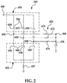
- the DC-DC voltage converter control circuit 240 has a terminal 446, a terminal 448, a high side FET IC 450, a low side FET IC 452, an intermediate circuit 453, a boost mode IC 454, a buck mode IC 456, and a resistor 457.
- the DC-DC voltage converter control circuit 240 can convert a DC voltage received at the terminal 446 to another DC voltage that is output at the terminal 448. Alternately, the DC-DC voltage converter control circuit 240 can convert a DC voltage received at the terminal 448 to another DC voltage that is output at the terminal 446.
- the high side FET IC 450 includes a plurality of FET switches 506 therein whose operational state (e.g., closed operational state or open operational state) is controlled by control voltages received by the DC-DC voltage converter control circuit 240.
- the plurality of FET switches 506 includes FET switches 650, 652, 654 which are electrically coupled at a first end to the terminal 446.
- the FET switch 650 is electrically coupled between the terminal 446 and the node 690, and is further electrically coupled in series with the FET switch 656 of the low side FET IC 452.
- the FET switch 652 is electrically coupled between the terminal 446 and the node 692, and is further electrically coupled in series with the FET switch 658 of the low side FET IC 452.
- the FET switch 654 is electrically coupled between the terminal 446 and the node 694, and further electrically coupled in series with the FET switch 660 of the low side FET IC 452.
- the low side FET IC 452 includes a plurality of FET switches 606 therein whose operational state (e.g., closed operational state or open operational state) is controlled by control voltages received by the DC-DC voltage converter control circuit 240.
- the plurality of FET switches 606 includes FET switches 656, 658, 660.
- the FET switch 656 is electrically coupled between the node 690 and a resistor 457, and is further electrically coupled in series with the FET switch 650 of the high side FET IC 450.
- the FET switch 658 is electrically coupled between the node 692 and the resistor 457, and is further electrically coupled in series with the FET switch 652 of the high side FET IC 450.
- the FET switch 660 is electrically coupled between the node 694 and the resistor 457, and is further electrically coupled in series with the FET switch 654 of the high side FET IC 450.
- the resistor 457 is further electrically coupled to the electrical ground of the battery 40.
- the intermediate circuit 453 includes resistors 670, 672, 674 and a capacitor 678.
- the resistor 670 is electrically coupled between the node 690 and the terminal 448.
- the resistor 672 is electrically coupled between the node 692 and the terminal 448.
- the resistor 674 is electrically coupled between the node 694 and the terminal 448.
- the capacitor 678 is electrically coupled between the terminal 448 and the electrical ground of the battery 56.
- the boost mode IC 454 is operably coupled to the FET switches 506 and 606 and is provided to control the FET switches 506 and 606 during the boost operational mode of the DC-DC voltage converter 54.
- the buck mode IC 454 is operably coupled to the FET switches 506 and 606 and is provided to control the FET switches 506 and 606 during the buck operational mode of the DC-DC voltage converter 54.
- the low voltage switch 270 is electrically coupled in parallel to the pre-charge low voltage switch 272 between and to electrical nodes 280, 282.
- the microcontroller 800 When the microcontroller 800 generates a control voltage (SWITCH_LV_OFF) having a high logic level that is received by the low voltage switch 270 (or that is received by a controller or a microprocessor within the DC-DC voltage converter 54 that is operably coupled to the switch 270), the microcontroller 800 induces the switch 270 to transition to a closed operational state.
- the microcontroller 800 generates the control voltage (SWITCH_LV_OFF) having a low logic level (e.g., ground voltage level)
- the microcontroller 800 induces the switch 270 to transition to an open operational state.
- the low voltage switch 270 is a FET switch such as a bi-directional MOSFET switch for example.
- the pre-charge low voltage switch 272 is electrically coupled between and to electrical nodes 280, 282.
- the microcontroller 800 When the microcontroller 800 generates a control voltage (C2) having a high logic level that is received by the pre-charge low voltage switch 272 (or that is received by a controller or a microprocessor within the DC-DC voltage converter 54 that is operably coupled to the switch 272), the microcontroller 800 induces the switch 272 to transition to a closed operational state.
- the microcontroller 800 generates the control voltage (C2) having a low logic level (e.g., ground voltage level)
- the microcontroller 800 induces the switch 272 to transition to an open operational state.
- the pre-charge low voltage switch 272 is a FET switch such as a bi-directional MOSFET switch for example.
- the battery 56 includes a positive terminal 780 and a negative terminal 782. In an exemplary embodiment, the battery 56 generates 12 Vdc between the positive terminal 780 and the negative terminal 782.
- the positive terminal 780 is electrically coupled to the electrical node 282 of the DC-DC voltage converter 54.
- the negative terminal 782 is electrically coupled to an electrical ground for the battery 56, which may be different that the electrical ground that the battery 40 is coupled to.
- the diagnostic system 58 is utilized to control the shutdown operations of the DC-DC voltage converter 54 when the diagnostic system 58 detects undesired operation of the DC-DC voltage converter 54.
- the diagnostic system 58 includes the microcontroller 800, the voltage drivers 802, 804, and the tri-state buffers 810, 812.
- the microcontroller 800 includes a microprocessor 940, the input-output (I/O) device 942, a memory device 944, and an analog-to-digital converter 946.
- the microprocessor 940 is operably coupled to the I/O device 942, the memory device 944, and the analog-to-digital converter 946, the DC-DC voltage converter 54, and the voltage drivers 802, 804.
- the tri-state buffer IC 810 is provided to receive control voltages from the microcontroller 800 and to output associated control voltages therefrom within a predetermined voltage range (e.g., 0 - 3.3 Vdc).
- the tri-state buffer IC 810 is provided to receive diagnostic signals from the DC-DC voltage converter 54 and to output associated diagnostic signals to the microcontroller 800 within the predetermined voltage range (e.g., 0 - 3.3 Vdc).
- the tri-state buffer IC 810 includes at least pins 1, 2, 6, 8, 9, 11, 12, 14, 15, 20 thereon.
- the pin 1 of the tri-state buffer IC 810 is electrically coupled to electrical ground.
- the pin 2 of the tri-state buffer IC 810 is electrically coupled to the pin 1 of the I/O device 942 of the microcontroller 800 and receives the control voltage (SWITCH_LV_OFF_SIG).
- SWITCH_LV_OFF_SIG the control voltage indicates that the low voltage switch 270 is to be transitioned to an open operational state.
- the pin 15 of the tri-state buffer IC 810 is electrically coupled to the low voltage switch 270.
- the pin 15 of the tri-state buffer IC 810 outputs the control voltage (SWITCH_LV_OFF) at a low logic level in response to the tri-state buffer IC 810 receiving the (SWITCH_LV_OFF_SIG) at a low logic level at pin 2 thereof.
- the low voltage switch 270 transitions to the open operational state in response to receiving the control voltage (SWITCH_LV_OFF) at the low logic level.
- the pin 6 of the tri-state buffer IC 810 is electrically coupled to the pin 1 of the DC-DC voltage converter control circuit 240, and receives the shutdown indicator voltage (SHUTDOWN_ISG_FETS_1) from the pin 1 of the DC-DC voltage converter control circuit 240.
- the shutdown indicator voltage (SHUTDOWN_ISG_FETS_1) has the high logic level
- the shutdown indicator voltage (SHUTDOWN_ISG_FETS_1) indicates that the plurality of FET switches 506 in the high side FET IC 450 have been transitioned to an open operational state, and the plurality of FET switches 606 in the low side FET IC 452 have been transitioned to the open operational state.
- the pin 14 of the tri-state buffer IC 810 is electrically coupled to the pin 2 of the I/O device 942 of the microcontroller 800 and outputs the shutdown indicator voltage (SHUTDOWN_ISG_FETS_1_DSP) having a high logic level, in response to the tri-state buffer IC 810 receiving the shutdown indicator voltage (SHUTDOWN_ISG_FETS_1) at the high logic level.
- the shutdown indicator voltage (SHUTDOWN_ISG_FETS_1_DSP) has the high logic level
- the shutdown indicator voltage (SHUTDOWN_ISG_FETS_1_DSP) indicates that the plurality of FET switches 506 in the high side FET IC 450 have been transitioned to the open operational state, and the plurality of FET switches 606 in the low side FET IC 452 have been transitioned to the open operational state.
- the pin 8 of the tri-state buffer IC 810 is electrically coupled to the pin 2 of the DC-DC voltage converter control circuit 240, and receives the electrical short indicator voltage (TRIP_ARM_SHORT_1) from the pin 2 of the DC-DC voltage converter control circuit 240.
- the electrical short indicator voltage (TRIP_ARM_SHORT_1) has the high logic level
- the electrical short indicator voltage (TRIP_ARM_SHORT_1) indicates that at least one FET in the plurality of FET switches 506 and the plurality of FET switches 606 has a short circuit condition to electrical ground.
- the pin 12 of the tri-state buffer IC 810 is electrically coupled to the pin 3 of the I/O device 942 of the microcontroller 800 and outputs the electrical short indicator voltage (TRIP_ARM_SHORT_1_DSP) having a high logic level, in response to the tri-state buffer IC 810 receiving the electrical short indicator voltage (TRIP_ARM_SHORT_1) at the high logic level.
- the electrical short indicator voltage (TRIP_ARM_SHORT_1_DSP) indicates that at least one FET in the plurality of FET switches 506 and the plurality of FET switches 606 has a short circuit condition to electrical ground.
- the pin 11 of the tri-state buffer IC 810 is electrically coupled to the pin 4 of the I/O device 942 of the microcontroller 800, and receives the control voltage (BOOST_IC_ENABLE_DSP) from the I/O device 942.
- the control voltage (BOOST_IC_ENABLE_DSP) has the high logic level
- the control voltage (BOOST_IC_ENABLE_DSP) indicates that boost mode IC 454 is to be activated such that the DC-DC voltage converter 54 is operated in the boost operational mode.
- the pin 9 of the tri-state buffer IC 810 is electrically coupled to the DC-DC voltage converter control circuit 240 and outputs the control voltage (BOOST_IC_ENABLE) having a high logic level, in response to the tri-state buffer IC 810 receiving the control voltage (BOOST_IC_ENABLE_DSP) at the high logic level.
- the control voltage (BOOST_IC_ENABLE_DSP) has the high logic level
- the control voltage (BOOST_IC_ENABLE_DSP) commands the boost mode IC to be activated for operating the FET switches 506 and 606 in a boost operational mode.
- the tri-state buffer IC 812 is provided to receive control voltages from the microcontroller 800 and to output associated control voltages therefrom within another predetermined voltage range (e.g., 0 - 5.0 Vdc).
- the tri-state buffer IC 812 is provided to receive diagnostic signals from the DC-DC voltage converter 54 and to output associated diagnostic signals to the microcontroller 800 within the other predetermined voltage range (e.g., 0 - 5.0 Vdc).
- the tri-state buffer IC 812 includes at least pins 1, 2, 6, 8, 9, 11, 12, 14, 15, 20.
- the pin 1 of the tri-state buffer IC 812 is electrically coupled to electrical ground.
- the pin 2 of the tri-state buffer IC 812 is electrically coupled to the pin 12 of the I/O device 942 of the microcontroller 800 and receives the control voltage (SWITCH_HV_OFF_SIG).
- SWITCH_HV_OFF_SIG the control voltage indicates that the high voltage switch 200 is to be transitioned to an open operational state.
- the pin 15 of the tri-state buffer IC 812 is electrically coupled to the high voltage switch 200.
- the pin 15 of the tri-state buffer IC 812 outputs the control voltage (SWITCH_HV_OFF) at a low logic level in response to the tri-state buffer IC 812 receiving the (SWITCH_HV_OFF_SIG) at pin 2 thereof.
- the high voltage switch 200 transitions to the open operational state in response to receiving the control voltage (SWITCH_HV_OFF) at the low logic level.
- the pin 6 of the tri-state buffer IC 812 is electrically coupled to the pin 4 of the DC-DC voltage converter control circuit 240, and receives the shutdown indicator voltage (SHUTDOWN_ISG_FETS_2) from the pin 4 of the DC-DC voltage converter control circuit 240.
- the shutdown indicator voltage (SHUTDOWN_ISG_FETS_2) has the high logic level
- the shutdown indicator voltage (SHUTDOWN_ISG_FETS_2) indicates that the plurality of FET switches 506 in the high side FET IC 450 have been transitioned to the open operational state, and the plurality of FET switches 606 in the low side FET IC 452 have been transitioned to the open operational state.
- the pin 14 of the tri-state buffer IC 812 is electrically coupled to the pin 5 of the I/O device 942 of the microcontroller 800 and outputs the shutdown indicator voltage (SHUTDOWN_ISG_FETS_2_DSP), in response to the tri-state buffer IC 812 receiving the shutdown indicator voltage (SHUTDOWN_ISG_FETS_2) at the high logic level.
- the shutdown indicator voltage (SHUTDOWN_ISG_FETS_2_DSP) has the high logic level
- the shutdown indicator voltage (SHUTDOWN_ISG_FETS_2_DSP) indicates that the plurality of FET switches 506 in the high side FET IC 450 have been transitioned to the open operational state, and the plurality of FET switches 606 in the low side FET IC 452 have been transitioned to the open operational state.
- the pin 8 of the tri-state buffer IC 812 is electrically coupled to the pin 5 of the DC-DC voltage converter control circuit 240, and receives the electrical short indicator voltage (TRIP_ARM_SHORT_2) from the pin 5 of the DC-DC voltage converter control circuit 240.
- the electrical short indicator voltage (TRIP_ARM_SHORT_2) has the high logic level
- the electrical short indicator voltage (TRIP_ARM_SHORT_2) indicates that at least one FET in the plurality of FET switches 506 and the plurality of FET switches 606 has a short circuit condition to electrical ground.
- the pin 12 of the tri-state buffer IC 810 is electrically coupled to the pin 6 of the I/O device 942 of the microcontroller 800 and outputs the electrical short indicator voltage (TRIP_ARM_SHORT_2_DSP) having a high logic level, in response to the tri-state buffer IC 812 receiving the electrical short indicator voltage (TRIP_ARM_SHORT_2) at the high logic level.
- the electrical short indicator voltage (TRIP_ARM_SHORT_2_DSP) indicates that at least one FET in the plurality of FET switches 506 and the plurality of FET switches 606 has a short circuit condition to electrical ground.
- the pin 11 of the tri-state buffer IC 812 is electrically coupled to the pin 7 of the I/O device 942 of the microcontroller 800, and receives the control voltage (BUCK_IC_ENABLE_DSP) from the I/O device 942.
- the control voltage (BUCK_IC_ENABLE_DSP) has the high logic level
- the control voltage (BUCK_IC_ENABLE_DSP) indicates that buck mode IC 456 is to be activated such that the DC-DC voltage converter 54 is to be operated in the buck operational mode.
- the pin 9 of the tri-state buffer IC 812 is electrically coupled to the pin 6 of the DC-DC voltage converter control circuit 240 and outputs the control voltage (BUCK_IC_ENABLE) having a high logic level, in response to the tri-state buffer IC 812 receiving the control voltage (BUCK_IC_ENABLE_DSP) at the high logic level.
- the control voltage (BUCK_IC_ENABLE_DSP) has the high logic level
- the control voltage (BUCK_IC_ENABLE_DSP) commands the buck mode IC to be activated for operating the FET switches 506 and 606 in a buck operational mode.
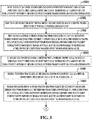
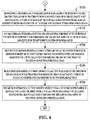
- FIGS. 1 , 3 and 4 a flowchart of a first diagnostic method for the DC-DC voltage converter 54 in accordance with another exemplary embodiment will be explained.
- the DC-DC voltage converter control circuit 240 outputs at the pin 1 a first shutdown indicator voltage (SHUTDOWN_ISG_FETS_1) indicating that the plurality of FET switches 506 in the high side FET IC 450 and the plurality of FET switches 606 in the low side FET IC 452 have been transitioned to an open operational state.
- the method advances to step 1502.
- the tri-state buffer IC 810 receives the first shutdown indicator voltage (SHUTDOWN_ISG_FETS_1) at the pin 6 thereof from the DC-DC voltage converter control circuit 240. After step 1502, the method advances to step 1504.
- the tri-state buffer IC 810 outputs a second shutdown indicator voltage (SHUTDOWN_ISG_FETS_1_DSP) at the pin 14 thereof in response to receiving the first shutdown indicator voltage (SHUTDOWN_ISG_FETS_1).
- the second shutdown indicator voltage (SHUTDOWN_ISG_FETS_1_DSP) is received by the microcontroller 800 and indicates that the plurality of FET switches 506 in the high side FET IC 450 and the plurality of FET switches 606 in the low side FET IC 452 have been transitioned to the open operational state.
- the method advances to step 1506.
- step 1506 the DC-DC voltage converter control circuit 240 outputs at the pin 4 a third shutdown indicator voltage (SHUTDOWN_ISG_FETS_2) indicating that the plurality of FET switches 506 in the high side FET IC 450 and the plurality of FET switches 606 in the low side FET IC 452 have been transitioned to the open operational state.
- step 1506 the method advances to step 1508.
- the tri-state buffer IC 812 receives the third shutdown indicator voltage (SHUTDOWN_ISG_FETS_2) at the pin 6 thereof from the DC-DC voltage converter control circuit 240. After step 1500, the method advances to step 1510.
- the tri-state buffer IC 812 outputs a fourth shutdown indicator voltage (SHUTDOWN_ISG_FETS_2_DSP) at the pin 14 thereof in response to receiving the third shutdown indicator voltage (SHUTDOWN_ISG_FETS_2).
- the fourth shutdown indicator voltage (SHUTDOWN_ISG_FETS_2_DSP) is received by the microcontroller 800 and indicates that the plurality of FET switches 506 in the high side FET IC 450 and the plurality of FET switches 606 in the low side FET IC 452 have been transitioned to the open operational state.
- the method advances step 1520.
- the microcontroller 800 stores a shutdown indicator flag in the memory device 944 indicating that the plurality of FET switches 506 in the high side FET IC 450 and the plurality of FET switches 606 in the low side FET IC 452 have been transitioned to the open operational state, in response to receiving at least one of the second and fourth shutdown indicator voltages (SHUTDOWN_ISG_FETS_1_DSP) (SHUTDOWN_ISG_FETS_2_DSP).
- the method advances to step 1522.
- the microcontroller 800 generates a first control voltage (SWITCH_LV_OFF_SIG) that is received at the pin 2 of the tri-state buffer IC 810 for commanding the low voltage switch 270 in the DC-DC voltage converter 54 to be transitioned to an open operational state.
- SWITCH_LV_OFF_SIG a first control voltage
- the tri-state buffer IC 810 outputs a second control voltage (SWITCH_LV_OFF) at the pin 15 thereof in response to receiving the first control voltage (SWITCH_LV_OFF_SIG).
- the second control voltage (SWITCH_LV_OFF) is received by the low voltage switch 270 and induces the low voltage switch 270 to transition to the open operational state.
- the method advances to step 1526.
- step 1526 the microcontroller 800 generates a third control voltage (SWITCH_HV_OFF_SIG) that is received at the pin 2 of the tri-state buffer IC 812 for commanding the high voltage switch 200 in the DC-DC voltage converter 54 to be transitioned to the open operational state.
- SWITCH_HV_OFF_SIG a third control voltage
- the tri-state buffer IC 812 outputs a fourth control voltage (SWITCH_HV_OFF) at the pin 15 thereof in response to receiving the third control voltage (SWITCH_HV_OFF_SIG).
- the fourth control voltage (SWITCH_HV_OFF) is received by the high voltage switch 200 and induces the high voltage switch 200 to transition to the open operational state.
- FIGS. 1 , 5 and 6 a flowchart of a second diagnostic method for the DC-DC voltage converter 54 in accordance with another exemplary embodiment will be explained.
- the DC-DC voltage converter control circuit 240 outputs at the pin 2 a first electrical short circuit indicator voltage (TRIP_ARM_SHORT_1) indicating that a first FET switch in one of the plurality of FET switches 506 in the high side FET IC 450 and the plurality of FET switches 606 in the low side FET IC 452 has a short circuit condition.
- TRIP_ARM_SHORT_1 a first electrical short circuit indicator voltage
- the tri-state buffer IC 810 receives the first electrical short circuit indicator voltage (TRIP_ARM_SHORT_1) at a high logic level at the pin 8 thereof from the DC-DC voltage converter control circuit 240. After step 1602, the method advances to step 1604.
- TRIP_ARM_SHORT_1 the first electrical short circuit indicator voltage
- the tri-state buffer IC 810 outputs a second electrical short circuit indicator voltage (TRIP_ARM_SHORT_1_DSP) at a high logic level at the pin 12 thereof in response to receiving the first electrical short circuit indicator voltage (TRIP_ARM_SHORT_1) at the high logic level.
- the second electrical short circuit indicator voltage (TRIP_ARM_SHORT_1_DSP) is received by the microcontroller 800 and indicates that the first FET switch in one of the plurality of FET switches 506 in the high side FET IC 450 and the plurality of FET switches 606 in the low side FET IC 452 has the short circuit condition.
- the method advances to step 1606.
- the DC-DC voltage converter control circuit 240 outputs at the pin 5 a third electrical short circuit indicator voltage (TRIP_ARM_SHORT_2) at a high logic level indicating that the first FET switch in one of the plurality of FET switches 506 in the high side FET IC 450 and the plurality of FET switches 606 in the low side FET IC 452 has a short circuit condition.
- the method advances to step 1608.
- the tri-state buffer IC 812 receives the third electrical short circuit indicator voltage (TRIP_ARM_SHORT_2) at the pin 8 thereof from the DC-DC voltage converter control circuit 240. After step 1608, the method advances to step 1620.
- TRIP_ARM_SHORT_2 the third electrical short circuit indicator voltage
- the tri-state buffer IC 812 outputs a fourth electrical short circuit indicator voltage (TRIP_ARM_SHORT_2_DSP) at a high logic level at the pin 12 thereof in response to receiving the third electrical short circuit indicator voltage (TRIP_ARM_SHORT_2) at the high logic level.
- the fourth electrical short circuit indicator voltage (TRIP_ARM_SHORT_2_DSP) is received by the microcontroller 800 and indicates that the first FET switch in one of the plurality of FET switches 506 in the high side FET IC 450 and the plurality of FET switches 606 in the low side FET IC 452 has the short circuit condition.
- the method advances to step 1622.
- the microcontroller 800 stores an electrical short indicator flag in the memory device 944 indicating that the first FET switch in one of the plurality of FET switches 506 in the high side FET IC 450 and the plurality of FET switches 606 in the low side FET IC 452 has the short circuit condition, in response to receiving at least one of the second and fourth electrical short circuit indicator voltages (TRIP_ARM_SHORT_1_DSP) (TRIP_ARM_SHORT_2_DSP).
- the method is exited.
- FIGS. 1 and 7 a flowchart of a third diagnostic method for the DC-DC voltage converter 54 in accordance with another exemplary embodiment will be explained.
- the microcontroller 800 generates a first control voltage (BOOST_IC_ENABLE_DSP) at a high logic level that is received at a pin 9 of the tri-state buffer IC 810 for commanding a boost mode IC 454 in a DC-DC voltage converter 54 to be activated.
- a first control voltage BOOST_IC_ENABLE_DSP
- the tri-state buffer IC 810 outputs a second control voltage (BOOST_IC_ENABLE) at a high logic level at a pin 9 thereof in response to receiving the first control voltage (BOOST_IC_ENABLE_DSP) at a high logic level.
- the second control voltage (BOOST_IC_ENABLE) is received by the boost mode IC 454 to induce the boost mode IC 454 to be activated at a first time, when a buck mode IC 456 is not activated.
- the method advances to step 1654.
- the microcontroller 800 generates a third control voltage (BUCK_IC_ENABLE_DSP) at a high logic level that is received at a pin 11 of the tri-state buffer IC 812 for commanding the buck mode IC in the DC-DC voltage converter 54 to be activated.
- BUCK_IC_ENABLE_DSP a third control voltage
- the tri-state buffer IC 812 outputs a fourth control voltage (BUCK_IC_ENABLE) at a high logic level at a pin 9 thereof in response to receiving the third control voltage (BUCK_IC_ENABLE_DSP) at a high logic level.
- the fourth control voltage (BUCK_IC_ENABLE) is received by the buck mode IC 456 to induce the buck mode IC 456 to be activated at a second time, when the boost mode IC 454 is not activated.
- the method is exited.
- the diagnostic system described herein provides a substantial advantage over other diagnostic systems.
- the diagnostic system diagnostic system utilizes a pair of tri-state buffers to independently control switches and integrated circuits within the DC-DC voltage converter, and to receive diagnostic signals from the DC-DC voltage converter.
Landscapes
- Engineering & Computer Science (AREA)
- Power Engineering (AREA)
- Physics & Mathematics (AREA)
- General Physics & Mathematics (AREA)
- Dc-Dc Converters (AREA)
Abstract
Description
- This application claims priority to
U.S. Provisional Patent Application No. 62/426,401 filed on November 25, 2016 U.S. Patent Application No. 15/808,967 filed on November 10, 2017 - A DC-DC voltage converter is a device for receiving an input voltage and generating an output voltage of a different level from the received input voltage and generally includes at least one switch. The DC-DC voltage converter may operate in various modes by means of mode shifting between a buck operational mode, a bust operational mode and the like.
- In order to diagnose the DC-DC voltage converter, in a conventional art, a single diagnosis integrated circuit is used to diagnose whether a plurality of FET switches in the DC-DC voltage converter are short-circuited. However, if the DC-DC voltage converter is diagnosed using the conventional single diagnosis integrated circuit, if the corresponding diagnosis integrated circuit does not operate, it is impossible to diagnose whether all of the plurality of FET switches in the DC-DC voltage converter are short-circuited.
- The inventor herein has recognized a need for an improved diagnostic system for a DC-DC voltage converter that utilizes a pair of tri-state buffer ICs to independently control switches and integrated circuits in the DC-DC voltage converter, and to receive diagnostic signals from the DC-DC voltage converter.
- These and other objects and advantages of the present disclosure may be understood from the following detailed description and will become more fully apparent from the exemplary embodiments of the present disclosure. Also, it will be easily understood that the objects and advantages of the present disclosure may be realized by the means shown in the appended claims and combinations thereof.
- Various embodiments of the present invention to accomplish the above object are as follows.
- A diagnostic system for a DC-DC voltage converter in accordance with an exemplary embodiment is provided.
- The DC-DC voltage converter has a high voltage switch, a low voltage switch, and a DC-DC voltage converter control circuit.
- The high voltage switch is electrically coupled between and to first and second electrical nodes.
- The low voltage switch is electrically coupled between and to third and fourth electrical nodes.
- The DC-DC voltage converter control circuit is electrically coupled between and to the second and third electrical nodes.
- The DC-DC voltage converter control circuit has a high side FET IC and a low side FET IC. The high side FET IC has a first plurality of FET switches therein. The low side FET IC has a second plurality of FET switches therein.
- Each FET switch of the first plurality of FET switches is electrically coupled to a respective FET switch of the second plurality of FET switches.
- The diagnostic system includes a first tri-state buffer IC having first and second pins. The diagnostic system further includes a second tri-state buffer IC having first and second pins. The diagnostic system further includes a microcontroller that is electrically coupled to the first and second tri-state buffer ICs.
- The first tri-state buffer IC receives a first shutdown indicator voltage at the first pin thereof from the DC-DC voltage converter control circuit indicating that the first plurality of FET switches in the high side FET IC and the second plurality of FET switches in the low side FET IC have been transitioned to an open operational state. The first tri-state buffer IC outputs a second shutdown indicator voltage at the second pin thereof in response to receiving the first shutdown indicator voltage. The second shutdown indicator voltage is received by the microcontroller and indicates that the first plurality of FET switches in the high side FET IC and the second plurality of FET switches in the low side FET IC have been transitioned to the open operational state.
- The second tri-state buffer IC receives a third shutdown indicator voltage at the first pin thereof from the DC-DC voltage converter control circuit indicating that the first plurality of FET switches in the high side FET IC and the second plurality of FET switches in the low side FET IC have been transitioned to the open operational state. The second tri-state buffer IC outputs a fourth shutdown indicator voltage at the second pin thereof in response to receiving the third shutdown indicator voltage. The fourth shutdown indicator voltage is received by the microcontroller and indicates that the first plurality of FET switches in the high side FET IC and the second plurality of FET switches in the low side FET IC have been transitioned to the open operational state.
- The microcontroller stores a shutdown indicator flag in a memory device indicating that the first plurality of FET switches in the high side FET IC and the second plurality of FET switches in the low side FET IC have been transitioned to the open operational state, in response to receiving at least one of the second and fourth shutdown indicator voltages.
- The fourth shutdown indicator voltage is greater than the second shutdown indicator voltage.
- The first tri-state buffer IC further has third and fourth pins.
- The second tri-state buffer IC further has third and fourth pins.
- The microcontroller generates a first control voltage that is received at the third pin of the first tri-state buffer IC for commanding the low voltage switch in the DC-DC voltage converter to be transitioned to an open operational state.
- The first tri-state buffer IC outputs a second control voltage at the fourth pin thereof in response to receiving the first control voltage, the second control voltage being received by the low voltage switch and inducing the low voltage switch to transition to the open operational state;
- The microcontroller generates a third control voltage that is received at the third pin of the second tri-state buffer IC for commanding the high voltage switch in the DC-DC voltage converter to be transitioned to the open operational state.
- The second tri-state buffer IC outputs a fourth control voltage at the fourth pin thereof in response to receiving the third control voltage, the fourth control voltage being received by the high voltage switch and inducing the high voltage switch to transition to the open operational state.
- The fourth control voltage is greater than the second control voltage.
- A diagnostic system for a DC-DC voltage converter in accordance with another exemplary embodiment is provided.
- The DC-DC voltage converter has a high voltage switch, a low voltage switch, and a DC-DC voltage converter control circuit.
- The high voltage switch is electrically coupled between and to first and second electrical nodes.
- The low voltage switch is electrically coupled between and to third and fourth electrical nodes.
- The DC-DC voltage converter control circuit is electrically coupled between and to the second and third electrical nodes.
- The DC-DC voltage converter control circuit has a high side FET IC and a low side FET IC. The high side FET IC has a first plurality of FET switches therein. The low side FET IC has a second plurality of FET switches therein.
- Each FET switch of the first plurality of FET switches is electrically coupled to a respective FET switch of the second plurality of FET switches.
- The diagnostic system includes a first tri-state buffer IC having first and second pins. The diagnostic system further includes a second tri-state buffer IC having first and second pins. The diagnostic system further includes a microcontroller that is electrically coupled to the first and second tri-state buffer ICs.
- The first tri-state buffer IC receives a first electrical short circuit indicator voltage at the first pin thereof from the DC-DC voltage converter control circuit indicating that a first FET switch in one of the first plurality of FET switches in the high side FET IC and the second plurality of FET switches in the low side FET IC has a short circuit condition. The first tri-state buffer IC outputs a second electrical short circuit indicator voltage at the second pin thereof in response to receiving the first electrical short circuit indicator voltage. The second electrical short circuit indicator voltage is received by the microcontroller and indicates that the first FET switch in one of the first plurality of FET switches in the high side FET IC and the second plurality of FET switches in the low side FET IC has the short circuit condition.
- The second tri-state buffer IC receives a third electrical short circuit indicator voltage at the first pin thereof from the DC-DC voltage converter control circuit indicating that the first FET switch in one of the first plurality of FET switches in the high side FET IC and the second plurality of FET switches in the low side FET IC has the short circuit condition. The second tri-state buffer IC outputs a fourth electrical short circuit indicator voltage at the second pin thereof in response to receiving the third electrical short circuit indicator voltage. The fourth electrical short circuit indicator voltage is received by the microcontroller and indicates that the first FET switch in one of the first plurality of FET switches in the high side FET IC and the second plurality of FET switches in the low side FET IC has the short circuit condition.
- The microcontroller stores an electrical short indicator flag in a memory device indicating that the first FET switch in one of the first plurality of FET switches in the high side FET IC and the second plurality of FET switches in the low side FET IC has the short circuit condition, in response to receiving at least one of the second and fourth electrical short circuit indicator voltages.
- The fourth electrical short circuit indicator voltage is greater than the second electrical short circuit indicator voltage.
- A diagnostic system for a DC-DC voltage converter in accordance with another exemplary embodiment is provided.
- The DC-DC voltage converter having a high voltage switch, a low voltage switch, and a boost mode IC and a buck mode IC.
- The high voltage switch being electrically coupled between and to first and second electrical nodes.
- The low voltage switch is electrically coupled between and to third and fourth electrical nodes.
- The boost mode IC is electrically coupled between and to second and third electrical nodes.
- The buck mode IC is electrically coupled between and to second and third electrical nodes.
- The diagnostic system includes a first tri-state buffer IC having first and second pins; a second tri-state buffer IC having first and second pins; and a microcontroller being electrically coupled to the first and second tri-state buffer ICs.
- The microcontroller generates a first control voltage that is received at the first pin of the first tri-state buffer IC for commanding the boost mode IC in the DC-DC voltage converter to be activated.
- The first tri-state buffer IC outputs a second control voltage at the second pin thereof in response to receiving the first control voltage, the second control voltage being received by the boost mode IC to induce the boost mode IC to be activated at a first time when the buck mode IC is not activated.
- The microcontroller generates a third control voltage that is received at the first pin of the second tri-state buffer IC for commanding the buck mode IC in the DC-DC voltage converter to be activated.
- The second tri-state buffer IC outputs a fourth control voltage at the second pin thereof in response to receiving the third control voltage, the fourth control voltage being received by the buck mode IC to induce the buck mode IC to be activated at a second time, when the boost mode IC is not activated.
- The fourth the fourth electrical short circuit indicator voltage is greater than the second electrical short circuit indicator voltage is greater than the second the fourth electrical short circuit indicator voltage is greater than the second electrical short circuit indicator voltage.
- According to at least one exemplary embodiment of the present invention, the diagnostic system of the DC-DC voltage converter independently controls the switches and the integrated circuits in the DC-DC voltage converter and receives diagnostic signals from the DC-DC voltage converter by using a pair of tri-state buffer ICs, so that the DC-DC voltage converter can be stably diagnosed even though any one of the pair of tri-state buffer ICs does not operate.
- The effects of the present invention are not limited to the above, and other effects not mentioned herein will be clearly understood from the appended claims by those skilled in the art.
- The accompanying drawings illustrate a preferred embodiment of the present disclosure and together with the foregoing disclosure, serve to provide further understanding of the technical features of the present disclosure, and thus, the present disclosure is not construed as being limited to the drawing.
-
FIG. 1 is a schematic of a vehicle having a diagnostic system for a DC-DC voltage converter in accordance with an exemplary embodiment; -
FIG. 2 is a schematic of a portion of a DC-DC voltage converter control circuit utilized in the DC-DC voltage converter ofFIG. 1 ; -
FIGS. 3-4 is a flowchart of a first diagnostic method performed by the diagnostic system ofFIG. 1 in accordance with an exemplary embodiment; -
FIGS. 5-6 is a flowchart of a second diagnostic method performed by the diagnostic system ofFIG. 1 in accordance with another exemplary embodiment; and -
FIG. 7 is a flowchart of a third diagnostic method performed by the diagnostic system ofFIG. 1 in accordance with an exemplary embodiment. - Hereinafter, preferred embodiments of the present disclosure will be described in detail with reference to the accompanying drawings. Prior to the description, it should be understood that the terms used in the specification and the appended claims should not be construed as limited to general and dictionary meanings, but interpreted based on the meanings and concepts corresponding to technical aspects of the present disclosure on the basis of the principle that the inventor is allowed to define terms appropriately for the best explanation.
- Therefore, the description proposed herein is just a preferable example for the purpose of illustrations only, not intended to limit the scope of the disclosure, so it should be understood that other equivalents and modifications could be made thereto without departing from the scope of the disclosure.
- In addition, in the present disclosure, if it is judged that detailed explanation on a known technique or configuration may unnecessarily make the essence of the present disclosure vague, the detailed explanation will be omitted.
- Throughout the specification, when a portion is referred to as "comprising" or "including" any element, it means that the portion may include other elements further, not excluding other elements unless specifically stated otherwise. Furthermore, the term "control unit" described in the specification refers to a unit that processes at least one function or operation, and may be implemented by hardware, software, or a combination of hardware and software.
- In addition, throughout the specification, when a portion is referred to as being "connected" to another portion, it is not limited to the case that they are "directly connected", but it also includes the case where they are "indirectly connected" with another element being interposed between them.
- Referring to
FIG. 1 , avehicle 10 is provided. Thevehicle 10 includes abattery 40, acontactor 42, a 3-phase capacitor bank 48, a battery-starter generator unit 50, a DC-DC voltage converter 54, abattery 56, adiagnostic system 58, andelectrical lines - An advantage of the
diagnostic system 58 is that thediagnostic system 58 utilizes two tri-state buffers to independently control switches and integrated circuits in the DC-DC voltage converter 54. - For purposes of understanding, some of the terms utilized herein will be described.
- The term "node" or "electrical node" is a region or a location in an electrical circuit.
- The term "signal" refers to one of an electrical voltage, an electrical current, and a binary value.
- The term "IC" refers to an integrated circuit.
- The term "FET" refers to a field-effect transistor.
- The term "FET switches" refers to a plurality of FET switches herein.
- The term "boost operational mode" refers to an operational mode of the DC-
DC voltage converter 54 in which the DC-DC voltage converter 54 applies a voltage to the 3-phase capacitor bank 48. In an exemplary embodiment, when the DC-DC voltage converter 54 has the boost operational mode, thecontactor 42 has an open operational state, thehigh voltage switch 200 has a closed operational state, the pre-chargehigh voltage switch 202 has a closed operational state, the FET switches 506, 606 are switched as desired, thelow voltage switch 270 has a closed operational state, and the pre-chargelow voltage switch 272 has a closed operational state. - The term "high logic level" corresponds to a voltage level associated with a binary "1", and the term "low logic level" corresponds to a voltage level associated with a binary "0."
- The term "tri-state buffer IC" refers a buffer IC that can have one of three states at each pin thereof. When the tri-state buffer IC receives an input signal within a first voltage range, the tri-state buffer IC outputs an associated signal at a low logic level. Further, when the tri-state buffer IC receives an input signal within a second voltage range, the tri-state buffer IC outputs an associated signal at a high logic level. Further, when the tri-state buffer IC receives an input signal a third voltage range between the first and second voltage ranges, the tri-state buffer IC does not output a signal.
- The
battery 40 includes apositive terminal 100 and anegative terminal 102. In an exemplary embodiment, thebattery 40 generates 48 Vdc between thepositive terminal 100 and thenegative terminal 102. Thepositive terminal 100 is electrically coupled to a firstelectrical node 124 on a first side of thecontactor 42. Thenegative terminal 102 is electrically coupled to an electrical ground for thebattery 40. - The
contactor 42 has acontactor coil 120, acontact 122, a firstelectrical node 124 and a secondelectrical node 126. The firstelectrical node 124 is electrically coupled to thepositive terminal 100 of thebattery 40. The secondelectrical node 126 is electrically coupled to both the 3-phase capacitor bank 48 and theelectrical node 210 of the DC-DC voltage converter 54. When themicrocontroller 800 generates first and second control signals that are received by thevoltage drivers contactor coil 120 is energized which transitions thecontact 122 to a closed operational state. Alternately, when themicrocontroller 800 generates third and fourth control signals that are received by thevoltage drivers contactor coil 120 is de-energized which transitions thecontact 122 to an open operational state. In an exemplary embodiment, the third and fourth control signals can each be a ground voltage level. - The 3-
phase capacitor bank 48 is utilized to store and release electrical energy from the battery starter-generator unit 50, thebattery 40, and the DC-DC voltage converter 54. The 3-phase capacitor bank 48 is electrically coupled to theelectrical node 126 of thecontactor 126 and theelectrical node 210 of the DC-DC voltage converter 54 utilizing theelectrical line 65. The 3-phase capacitor bank 48 is further electrically coupled to the battery-starter generator 50 utilizing theelectrical lines - The battery-
starter generator unit 50 is provided to generate an AC voltage that is received by the 3-phase capacitor bank 48 via theelectrical lines - The DC-
DC voltage converter 54 includes ahigh voltage switch 200, a pre-chargehigh voltage switch 202,electrical nodes converter control circuit 240, alow voltage switch 270, a pre-chargelow voltage switch 272,electrical nodes electrical lines - The
high voltage switch 200 is electrically coupled between anode 210 and anode 212. Thenode 212 is electrically coupled to theterminal 446 of the DC-DC voltageconverter control circuit 240. Thenode 210 is electrically coupled to thenode 126 of thecontactor 42. When themicrocontroller 800 generates a control voltage (SWITCH_HV_OFF) having a high logic level that is received by the high voltage switch 200 (or that is received by a controller or a microprocessor within the DC-DC voltage converter 54 that is operably coupled to the switch 200), themicrocontroller 800 induces theswitch 200 to transition to a closed operational state. When themicrocontroller 800 generates the control voltage (SWITCH_HV_OFF) having a low logic level (e.g., ground voltage level), themicrocontroller 800 induces theswitch 200 to transition to an open operational state. In an exemplary embodiment, thehigh voltage switch 200 is a FET switch such as a bi-directional MOSFET switch for example. - The pre-charge
high voltage switch 202 is electrically coupled between thenode 210 and thenode 212. When themicrocontroller 800 generates a control voltage (C1) having a high logic level that is received by the pre-charge high voltage switch 202 (or that is received by a controller or a microprocessor within the DC-DC voltage converter 54 that is operably coupled to the switch 202), themicrocontroller 800 induces theswitch 202 to transition to a closed operational state. When themicrocontroller 800 generates the control voltage (C1) having a low logic level (e.g., ground voltage level), themicrocontroller 800 induces theswitch 202 to transition to an open operational state. In an exemplary embodiment, the pre-chargehigh voltage switch 202 is a FET switch such as a bi-directional MOSFET switch for example.** - Referring to
FIGS. 1 and2 , the DC-DC voltageconverter control circuit 240 has a terminal 446, a terminal 448, a highside FET IC 450, a lowside FET IC 452, anintermediate circuit 453, aboost mode IC 454, abuck mode IC 456, and aresistor 457. The DC-DC voltageconverter control circuit 240 can convert a DC voltage received at the terminal 446 to another DC voltage that is output at the terminal 448. Alternately, the DC-DC voltageconverter control circuit 240 can convert a DC voltage received at the terminal 448 to another DC voltage that is output at the terminal 446. - The high
side FET IC 450 includes a plurality of FET switches 506 therein whose operational state (e.g., closed operational state or open operational state) is controlled by control voltages received by the DC-DC voltageconverter control circuit 240. In an exemplary embodiment, the plurality of FET switches 506 includes FET switches 650, 652, 654 which are electrically coupled at a first end to the terminal 446. TheFET switch 650 is electrically coupled between the terminal 446 and thenode 690, and is further electrically coupled in series with theFET switch 656 of the lowside FET IC 452. TheFET switch 652 is electrically coupled between the terminal 446 and thenode 692, and is further electrically coupled in series with theFET switch 658 of the lowside FET IC 452. TheFET switch 654 is electrically coupled between the terminal 446 and thenode 694, and further electrically coupled in series with theFET switch 660 of the lowside FET IC 452. - The low
side FET IC 452 includes a plurality of FET switches 606 therein whose operational state (e.g., closed operational state or open operational state) is controlled by control voltages received by the DC-DC voltageconverter control circuit 240. In an exemplary embodiment, the plurality of FET switches 606 includes FET switches 656, 658, 660. TheFET switch 656 is electrically coupled between thenode 690 and aresistor 457, and is further electrically coupled in series with theFET switch 650 of the highside FET IC 450. TheFET switch 658 is electrically coupled between thenode 692 and theresistor 457, and is further electrically coupled in series with theFET switch 652 of the highside FET IC 450. TheFET switch 660 is electrically coupled between thenode 694 and theresistor 457, and is further electrically coupled in series with theFET switch 654 of the highside FET IC 450. Theresistor 457 is further electrically coupled to the electrical ground of thebattery 40. - The
intermediate circuit 453 includesresistors capacitor 678. Theresistor 670 is electrically coupled between thenode 690 and the terminal 448. Theresistor 672 is electrically coupled between thenode 692 and the terminal 448. Further, theresistor 674 is electrically coupled between thenode 694 and the terminal 448. Thecapacitor 678 is electrically coupled between the terminal 448 and the electrical ground of thebattery 56. - The
boost mode IC 454 is operably coupled to the FET switches 506 and 606 and is provided to control the FET switches 506 and 606 during the boost operational mode of the DC-DC voltage converter 54. - The
buck mode IC 454 is operably coupled to the FET switches 506 and 606 and is provided to control the FET switches 506 and 606 during the buck operational mode of the DC-DC voltage converter 54. - Referring to
FIG. 1 , thelow voltage switch 270 is electrically coupled in parallel to the pre-chargelow voltage switch 272 between and toelectrical nodes microcontroller 800 generates a control voltage (SWITCH_LV_OFF) having a high logic level that is received by the low voltage switch 270 (or that is received by a controller or a microprocessor within the DC-DC voltage converter 54 that is operably coupled to the switch 270), themicrocontroller 800 induces theswitch 270 to transition to a closed operational state. When themicrocontroller 800 generates the control voltage (SWITCH_LV_OFF) having a low logic level (e.g., ground voltage level), themicrocontroller 800 induces theswitch 270 to transition to an open operational state. In an exemplary embodiment, thelow voltage switch 270 is a FET switch such as a bi-directional MOSFET switch for example. - The pre-charge
low voltage switch 272 is electrically coupled between and toelectrical nodes microcontroller 800 generates a control voltage (C2) having a high logic level that is received by the pre-charge low voltage switch 272 (or that is received by a controller or a microprocessor within the DC-DC voltage converter 54 that is operably coupled to the switch 272), themicrocontroller 800 induces theswitch 272 to transition to a closed operational state. When themicrocontroller 800 generates the control voltage (C2) having a low logic level (e.g., ground voltage level), themicrocontroller 800 induces theswitch 272 to transition to an open operational state. In an exemplary embodiment, the pre-chargelow voltage switch 272 is a FET switch such as a bi-directional MOSFET switch for example. - The
battery 56 includes apositive terminal 780 and anegative terminal 782. In an exemplary embodiment, thebattery 56 generates 12 Vdc between thepositive terminal 780 and thenegative terminal 782. Thepositive terminal 780 is electrically coupled to theelectrical node 282 of the DC-DC voltage converter 54. Thenegative terminal 782 is electrically coupled to an electrical ground for thebattery 56, which may be different that the electrical ground that thebattery 40 is coupled to. - The
diagnostic system 58 is utilized to control the shutdown operations of the DC-DC voltage converter 54 when thediagnostic system 58 detects undesired operation of the DC-DC voltage converter 54. Thediagnostic system 58 includes themicrocontroller 800, thevoltage drivers tri-state buffers - The
microcontroller 800 includes amicroprocessor 940, the input-output (I/O)device 942, amemory device 944, and an analog-to-digital converter 946. Themicroprocessor 940 is operably coupled to the I/O device 942, thememory device 944, and the analog-to-digital converter 946, the DC-DC voltage converter 54, and thevoltage drivers - The
tri-state buffer IC 810 is provided to receive control voltages from themicrocontroller 800 and to output associated control voltages therefrom within a predetermined voltage range (e.g., 0 - 3.3 Vdc). Thetri-state buffer IC 810 is provided to receive diagnostic signals from the DC-DC voltage converter 54 and to output associated diagnostic signals to themicrocontroller 800 within the predetermined voltage range (e.g., 0 - 3.3 Vdc). - The
tri-state buffer IC 810 includes atleast pins - The
pin 1 of thetri-state buffer IC 810 is electrically coupled to electrical ground. - The
pin 2 of thetri-state buffer IC 810 is electrically coupled to thepin 1 of the I/O device 942 of themicrocontroller 800 and receives the control voltage (SWITCH_LV_OFF_SIG). When the control voltage (SWITCH_LV_OFF_SIG) has a low logic level, the control voltage indicates that thelow voltage switch 270 is to be transitioned to an open operational state. - The
pin 15 of thetri-state buffer IC 810 is electrically coupled to thelow voltage switch 270. Thepin 15 of thetri-state buffer IC 810 outputs the control voltage (SWITCH_LV_OFF) at a low logic level in response to thetri-state buffer IC 810 receiving the (SWITCH_LV_OFF_SIG) at a low logic level atpin 2 thereof. Thelow voltage switch 270 transitions to the open operational state in response to receiving the control voltage (SWITCH_LV_OFF) at the low logic level. - The
pin 6 of thetri-state buffer IC 810 is electrically coupled to thepin 1 of the DC-DC voltageconverter control circuit 240, and receives the shutdown indicator voltage (SHUTDOWN_ISG_FETS_1) from thepin 1 of the DC-DC voltageconverter control circuit 240. When the shutdown indicator voltage (SHUTDOWN_ISG_FETS_1) has the high logic level, the shutdown indicator voltage (SHUTDOWN_ISG_FETS_1) indicates that the plurality of FET switches 506 in the highside FET IC 450 have been transitioned to an open operational state, and the plurality of FET switches 606 in the lowside FET IC 452 have been transitioned to the open operational state. - The
pin 14 of thetri-state buffer IC 810 is electrically coupled to thepin 2 of the I/O device 942 of themicrocontroller 800 and outputs the shutdown indicator voltage (SHUTDOWN_ISG_FETS_1_DSP) having a high logic level, in response to thetri-state buffer IC 810 receiving the shutdown indicator voltage (SHUTDOWN_ISG_FETS_1) at the high logic level. When the shutdown indicator voltage (SHUTDOWN_ISG_FETS_1_DSP) has the high logic level, the shutdown indicator voltage (SHUTDOWN_ISG_FETS_1_DSP) indicates that the plurality of FET switches 506 in the highside FET IC 450 have been transitioned to the open operational state, and the plurality of FET switches 606 in the lowside FET IC 452 have been transitioned to the open operational state. - The pin 8 of the
tri-state buffer IC 810 is electrically coupled to thepin 2 of the DC-DC voltageconverter control circuit 240, and receives the electrical short indicator voltage (TRIP_ARM_SHORT_1) from thepin 2 of the DC-DC voltageconverter control circuit 240. When the electrical short indicator voltage (TRIP_ARM_SHORT_1) has the high logic level, the electrical short indicator voltage (TRIP_ARM_SHORT_1) indicates that at least one FET in the plurality of FET switches 506 and the plurality of FET switches 606 has a short circuit condition to electrical ground. - The
pin 12 of thetri-state buffer IC 810 is electrically coupled to thepin 3 of the I/O device 942 of themicrocontroller 800 and outputs the electrical short indicator voltage (TRIP_ARM_SHORT_1_DSP) having a high logic level, in response to thetri-state buffer IC 810 receiving the electrical short indicator voltage (TRIP_ARM_SHORT_1) at the high logic level. When the electrical short indicator voltage (TRIP_ARM_SHORT_1_DSP) has the high logic level, the electrical short indicator voltage (TRIP_ARM_SHORT_1_DSP) indicates that at least one FET in the plurality of FET switches 506 and the plurality of FET switches 606 has a short circuit condition to electrical ground. - The
pin 11 of thetri-state buffer IC 810 is electrically coupled to the pin 4 of the I/O device 942 of themicrocontroller 800, and receives the control voltage (BOOST_IC_ENABLE_DSP) from the I/O device 942. When the control voltage (BOOST_IC_ENABLE_DSP) has the high logic level, the control voltage (BOOST_IC_ENABLE_DSP) indicates thatboost mode IC 454 is to be activated such that the DC-DC voltage converter 54 is operated in the boost operational mode. - The pin 9 of the
tri-state buffer IC 810 is electrically coupled to the DC-DC voltageconverter control circuit 240 and outputs the control voltage (BOOST_IC_ENABLE) having a high logic level, in response to thetri-state buffer IC 810 receiving the control voltage (BOOST_IC_ENABLE_DSP) at the high logic level. When the control voltage (BOOST_IC_ENABLE_DSP) has the high logic level, the control voltage (BOOST_IC_ENABLE_DSP) commands the boost mode IC to be activated for operating the FET switches 506 and 606 in a boost operational mode. - The
tri-state buffer IC 812 is provided to receive control voltages from themicrocontroller 800 and to output associated control voltages therefrom within another predetermined voltage range (e.g., 0 - 5.0 Vdc). Thetri-state buffer IC 812 is provided to receive diagnostic signals from the DC-DC voltage converter 54 and to output associated diagnostic signals to themicrocontroller 800 within the other predetermined voltage range (e.g., 0 - 5.0 Vdc). Thetri-state buffer IC 812 includes atleast pins - The
pin 1 of thetri-state buffer IC 812 is electrically coupled to electrical ground. - The
pin 2 of thetri-state buffer IC 812 is electrically coupled to thepin 12 of the I/O device 942 of themicrocontroller 800 and receives the control voltage (SWITCH_HV_OFF_SIG). When the control voltage (SWITCH_HV_OFF_SIG) has a low logic level, the control voltage indicates that thehigh voltage switch 200 is to be transitioned to an open operational state. - The
pin 15 of thetri-state buffer IC 812 is electrically coupled to thehigh voltage switch 200. Thepin 15 of thetri-state buffer IC 812 outputs the control voltage (SWITCH_HV_OFF) at a low logic level in response to thetri-state buffer IC 812 receiving the (SWITCH_HV_OFF_SIG) atpin 2 thereof. Thehigh voltage switch 200 transitions to the open operational state in response to receiving the control voltage (SWITCH_HV_OFF) at the low logic level. - The
pin 6 of thetri-state buffer IC 812 is electrically coupled to the pin 4 of the DC-DC voltageconverter control circuit 240, and receives the shutdown indicator voltage (SHUTDOWN_ISG_FETS_2) from the pin 4 of the DC-DC voltageconverter control circuit 240. When the shutdown indicator voltage (SHUTDOWN_ISG_FETS_2) has the high logic level, the shutdown indicator voltage (SHUTDOWN_ISG_FETS_2) indicates that the plurality of FET switches 506 in the highside FET IC 450 have been transitioned to the open operational state, and the plurality of FET switches 606 in the lowside FET IC 452 have been transitioned to the open operational state. - The
pin 14 of thetri-state buffer IC 812 is electrically coupled to thepin 5 of the I/O device 942 of themicrocontroller 800 and outputs the shutdown indicator voltage (SHUTDOWN_ISG_FETS_2_DSP), in response to thetri-state buffer IC 812 receiving the shutdown indicator voltage (SHUTDOWN_ISG_FETS_2) at the high logic level. When the shutdown indicator voltage (SHUTDOWN_ISG_FETS_2_DSP) has the high logic level, the shutdown indicator voltage (SHUTDOWN_ISG_FETS_2_DSP) indicates that the plurality of FET switches 506 in the highside FET IC 450 have been transitioned to the open operational state, and the plurality of FET switches 606 in the lowside FET IC 452 have been transitioned to the open operational state. - The pin 8 of the
tri-state buffer IC 812 is electrically coupled to thepin 5 of the DC-DC voltageconverter control circuit 240, and receives the electrical short indicator voltage (TRIP_ARM_SHORT_2) from thepin 5 of the DC-DC voltageconverter control circuit 240. When the electrical short indicator voltage (TRIP_ARM_SHORT_2) has the high logic level, the electrical short indicator voltage (TRIP_ARM_SHORT_2) indicates that at least one FET in the plurality of FET switches 506 and the plurality of FET switches 606 has a short circuit condition to electrical ground. - The
pin 12 of thetri-state buffer IC 810 is electrically coupled to thepin 6 of the I/O device 942 of themicrocontroller 800 and outputs the electrical short indicator voltage (TRIP_ARM_SHORT_2_DSP) having a high logic level, in response to thetri-state buffer IC 812 receiving the electrical short indicator voltage (TRIP_ARM_SHORT_2) at the high logic level. When the electrical short indicator voltage (TRIP_ARM_SHORT_2_DSP) has the high logic level, the electrical short indicator voltage (TRIP_ARM_SHORT_2_DSP) indicates that at least one FET in the plurality of FET switches 506 and the plurality of FET switches 606 has a short circuit condition to electrical ground. - The
pin 11 of thetri-state buffer IC 812 is electrically coupled to the pin 7 of the I/O device 942 of themicrocontroller 800, and receives the control voltage (BUCK_IC_ENABLE_DSP) from the I/O device 942. When the control voltage (BUCK_IC_ENABLE_DSP) has the high logic level, the control voltage (BUCK_IC_ENABLE_DSP) indicates thatbuck mode IC 456 is to be activated such that the DC-DC voltage converter 54 is to be operated in the buck operational mode. - The pin 9 of the
tri-state buffer IC 812 is electrically coupled to thepin 6 of the DC-DC voltageconverter control circuit 240 and outputs the control voltage (BUCK_IC_ENABLE) having a high logic level, in response to thetri-state buffer IC 812 receiving the control voltage (BUCK_IC_ENABLE_DSP) at the high logic level. When the control voltage (BUCK_IC_ENABLE_DSP) has the high logic level, the control voltage (BUCK_IC_ENABLE_DSP) commands the buck mode IC to be activated for operating the FET switches 506 and 606 in a buck operational mode. - Referring to
FIGS. 1 ,3 and4 , a flowchart of a first diagnostic method for the DC-DC voltage converter 54 in accordance with another exemplary embodiment will be explained. - At
step 1500, the DC-DC voltageconverter control circuit 240 outputs at the pin 1 a first shutdown indicator voltage (SHUTDOWN_ISG_FETS_1) indicating that the plurality of FET switches 506 in the highside FET IC 450 and the plurality of FET switches 606 in the lowside FET IC 452 have been transitioned to an open operational state. Afterstep 1500, the method advances to step 1502. - At
step 1502, thetri-state buffer IC 810 receives the first shutdown indicator voltage (SHUTDOWN_ISG_FETS_1) at thepin 6 thereof from the DC-DC voltageconverter control circuit 240. Afterstep 1502, the method advances to step 1504. - At
step 1504, thetri-state buffer IC 810 outputs a second shutdown indicator voltage (SHUTDOWN_ISG_FETS_1_DSP) at thepin 14 thereof in response to receiving the first shutdown indicator voltage (SHUTDOWN_ISG_FETS_1). The second shutdown indicator voltage (SHUTDOWN_ISG_FETS_1_DSP) is received by themicrocontroller 800 and indicates that the plurality of FET switches 506 in the highside FET IC 450 and the plurality of FET switches 606 in the lowside FET IC 452 have been transitioned to the open operational state. Afterstep 1504, the method advances to step 1506. - At
step 1506, the DC-DC voltageconverter control circuit 240 outputs at the pin 4 a third shutdown indicator voltage (SHUTDOWN_ISG_FETS_2) indicating that the plurality of FET switches 506 in the highside FET IC 450 and the plurality of FET switches 606 in the lowside FET IC 452 have been transitioned to the open operational state. Afterstep 1506, the method advances to step 1508. - At
step 1508, thetri-state buffer IC 812 receives the third shutdown indicator voltage (SHUTDOWN_ISG_FETS_2) at thepin 6 thereof from the DC-DC voltageconverter control circuit 240. Afterstep 1500, the method advances to step 1510. - At
step 1510, thetri-state buffer IC 812 outputs a fourth shutdown indicator voltage (SHUTDOWN_ISG_FETS_2_DSP) at thepin 14 thereof in response to receiving the third shutdown indicator voltage (SHUTDOWN_ISG_FETS_2). The fourth shutdown indicator voltage (SHUTDOWN_ISG_FETS_2_DSP) is received by themicrocontroller 800 and indicates that the plurality of FET switches 506 in the highside FET IC 450 and the plurality of FET switches 606 in the lowside FET IC 452 have been transitioned to the open operational state. Afterstep 1510, the method advancesstep 1520. - At
step 1520, themicrocontroller 800 stores a shutdown indicator flag in thememory device 944 indicating that the plurality of FET switches 506 in the highside FET IC 450 and the plurality of FET switches 606 in the lowside FET IC 452 have been transitioned to the open operational state, in response to receiving at least one of the second and fourth shutdown indicator voltages (SHUTDOWN_ISG_FETS_1_DSP) (SHUTDOWN_ISG_FETS_2_DSP). Afterstep 1520, the method advances to step 1522. - At
step 1522, themicrocontroller 800 generates a first control voltage (SWITCH_LV_OFF_SIG) that is received at thepin 2 of thetri-state buffer IC 810 for commanding thelow voltage switch 270 in the DC-DC voltage converter 54 to be transitioned to an open operational state. Afterstep 1522, the method advances to step 1524. - At
step 1524, thetri-state buffer IC 810 outputs a second control voltage (SWITCH_LV_OFF) at thepin 15 thereof in response to receiving the first control voltage (SWITCH_LV_OFF_SIG). The second control voltage (SWITCH_LV_OFF) is received by thelow voltage switch 270 and induces thelow voltage switch 270 to transition to the open operational state. Afterstep 1524, the method advances to step 1526. - At
step 1526, themicrocontroller 800 generates a third control voltage (SWITCH_HV_OFF_SIG) that is received at thepin 2 of thetri-state buffer IC 812 for commanding thehigh voltage switch 200 in the DC-DC voltage converter 54 to be transitioned to the open operational state. Afterstep 1526, the method advances to step 1528. - At
step 1528, thetri-state buffer IC 812 outputs a fourth control voltage (SWITCH_HV_OFF) at thepin 15 thereof in response to receiving the third control voltage (SWITCH_HV_OFF_SIG). The fourth control voltage (SWITCH_HV_OFF) is received by thehigh voltage switch 200 and induces thehigh voltage switch 200 to transition to the open operational state. Afterstep 1528, the method is exited. - Referring to
FIGS. 1 ,5 and6 , a flowchart of a second diagnostic method for the DC-DC voltage converter 54 in accordance with another exemplary embodiment will be explained. - At
step 1600, the DC-DC voltageconverter control circuit 240 outputs at the pin 2 a first electrical short circuit indicator voltage (TRIP_ARM_SHORT_1) indicating that a first FET switch in one of the plurality of FET switches 506 in the highside FET IC 450 and the plurality of FET switches 606 in the lowside FET IC 452 has a short circuit condition. Afterstep 1600, the method advances to step 1602. - At
step 1602, thetri-state buffer IC 810 receives the first electrical short circuit indicator voltage (TRIP_ARM_SHORT_1) at a high logic level at the pin 8 thereof from the DC-DC voltageconverter control circuit 240. Afterstep 1602, the method advances to step 1604. - At
step 1604, thetri-state buffer IC 810 outputs a second electrical short circuit indicator voltage (TRIP_ARM_SHORT_1_DSP) at a high logic level at thepin 12 thereof in response to receiving the first electrical short circuit indicator voltage (TRIP_ARM_SHORT_1) at the high logic level. The second electrical short circuit indicator voltage (TRIP_ARM_SHORT_1_DSP) is received by themicrocontroller 800 and indicates that the first FET switch in one of the plurality of FET switches 506 in the highside FET IC 450 and the plurality of FET switches 606 in the lowside FET IC 452 has the short circuit condition. Afterstep 1604, the method advances to step 1606. - At
step 1606, the DC-DC voltageconverter control circuit 240 outputs at the pin 5 a third electrical short circuit indicator voltage (TRIP_ARM_SHORT_2) at a high logic level indicating that the first FET switch in one of the plurality of FET switches 506 in the highside FET IC 450 and the plurality of FET switches 606 in the lowside FET IC 452 has a short circuit condition. Afterstep 1606, the method advances to step 1608. - At
step 1608, thetri-state buffer IC 812 receives the third electrical short circuit indicator voltage (TRIP_ARM_SHORT_2) at the pin 8 thereof from the DC-DC voltageconverter control circuit 240. Afterstep 1608, the method advances to step 1620. - At
step 1620, thetri-state buffer IC 812 outputs a fourth electrical short circuit indicator voltage (TRIP_ARM_SHORT_2_DSP) at a high logic level at thepin 12 thereof in response to receiving the third electrical short circuit indicator voltage (TRIP_ARM_SHORT_2) at the high logic level. The fourth electrical short circuit indicator voltage (TRIP_ARM_SHORT_2_DSP) is received by themicrocontroller 800 and indicates that the first FET switch in one of the plurality of FET switches 506 in the highside FET IC 450 and the plurality of FET switches 606 in the lowside FET IC 452 has the short circuit condition. Afterstep 1620, the method advances to step 1622. - At
step 1622, themicrocontroller 800 stores an electrical short indicator flag in thememory device 944 indicating that the first FET switch in one of the plurality of FET switches 506 in the highside FET IC 450 and the plurality of FET switches 606 in the lowside FET IC 452 has the short circuit condition, in response to receiving at least one of the second and fourth electrical short circuit indicator voltages (TRIP_ARM_SHORT_1_DSP) (TRIP_ARM_SHORT_2_DSP). Afterstep 1622, the method is exited. - Referring to
FIGS. 1 and7 , a flowchart of a third diagnostic method for the DC-DC voltage converter 54 in accordance with another exemplary embodiment will be explained. - At
step 1650, themicrocontroller 800 generates a first control voltage (BOOST_IC_ENABLE_DSP) at a high logic level that is received at a pin 9 of thetri-state buffer IC 810 for commanding aboost mode IC 454 in a DC-DC voltage converter 54 to be activated. Afterstep 1650, the method advances to step 1652. - At
step 1652, thetri-state buffer IC 810 outputs a second control voltage (BOOST_IC_ENABLE) at a high logic level at a pin 9 thereof in response to receiving the first control voltage (BOOST_IC_ENABLE_DSP) at a high logic level. The second control voltage (BOOST_IC_ENABLE) is received by theboost mode IC 454 to induce theboost mode IC 454 to be activated at a first time, when abuck mode IC 456 is not activated. Afterstep 1652, the method advances to step 1654. - At
step 1654, themicrocontroller 800 generates a third control voltage (BUCK_IC_ENABLE_DSP) at a high logic level that is received at apin 11 of thetri-state buffer IC 812 for commanding the buck mode IC in the DC-DC voltage converter 54 to be activated. Afterstep 1654, the method advances to step 1656. - At
step 1656, thetri-state buffer IC 812 outputs a fourth control voltage (BUCK_IC_ENABLE) at a high logic level at a pin 9 thereof in response to receiving the third control voltage (BUCK_IC_ENABLE_DSP) at a high logic level. The fourth control voltage (BUCK_IC_ENABLE) is received by thebuck mode IC 456 to induce thebuck mode IC 456 to be activated at a second time, when theboost mode IC 454 is not activated. Afterstep 1656, the method is exited. - The diagnostic system described herein provides a substantial advantage over other diagnostic systems. In particular, the diagnostic system diagnostic system utilizes a pair of tri-state buffers to independently control switches and integrated circuits within the DC-DC voltage converter, and to receive diagnostic signals from the DC-DC voltage converter.
- While the claimed invention has been described in detail in connection with only a limited number of embodiments, it should be readily understood that the invention is not limited to such disclosed embodiments. Rather, the claimed invention can be modified to incorporate any number of variations, alterations, substitutions or equivalent arrangements not heretofore described, but which are commensurate with the spirit and scope of the invention. Additionally, while various embodiments of the claimed invention have been described, it is to be understood that aspects of the invention may include only some of the described embodiments. Accordingly, the claimed invention is not to be seen as limited by the foregoing description.
- The embodiments of the present invention described above are not necessarily implemented only by the apparatus and the method, but may be implemented through a program realizing the function corresponding to the configuration of the embodiment of the present invention or a recording medium on which the program is recorded. These embodiments can be easily implemented by those skilled in the art from the above description of the embodiments.
Claims (8)
- A diagnostic system for a DC-DC voltage converter, the DC-DC voltage converter having a high voltage switch, a low voltage switch, and a DC-DC voltage converter control circuit; the high voltage switch being electrically coupled between and to first and second electrical nodes; the low voltage switch being electrically coupled between and to third and fourth electrical nodes; the DC-DC voltage converter control circuit being electrically coupled between and to the second and third electrical nodes; the DC-DC voltage converter control circuit having a high side FET IC and a low side FET IC; the high side FET IC having a first plurality of FET switches therein, the low side FET IC having a second plurality of FET switches therein, each FET switch of the first plurality of FET switches being electrically coupled to a respective FET switch of the second plurality of FET switches, the diagnostic system comprising:a first tri-state buffer IC having first and second pins;a second tri-state buffer IC having first and second pins;a microcontroller being electrically coupled to the first and second tri-state buffer ICs;the first tri-state buffer IC receiving a first shutdown indicator voltage at the first pin thereof from the DC-DC voltage converter control circuit indicating that the first plurality of FET switches in the high side FET IC and the second plurality of FET switches in the low side FET IC have been transitioned to an open operational state;the first tri-state buffer IC outputting a second shutdown indicator voltage at the second pin thereof in response to receiving the first shutdown indicator voltage, the second shutdown indicator voltage being received by the microcontroller and indicating that the first plurality of FET switches in the high side FET IC and the second plurality of FET switches in the low side FET IC have been transitioned to the open operational state;the second tri-state buffer IC receiving a third shutdown indicator voltage at the first pin thereof from the DC-DC voltage converter control circuit indicating that the first plurality of FET switches in the high side FET IC and the second plurality of FET switches in the low side FET IC have been transitioned to the open operational state;the second tri-state buffer IC outputting a fourth shutdown indicator voltage at the second pin thereof in response to receiving the third shutdown indicator voltage, the fourth shutdown indicator voltage being received by the microcontroller and indicating that the first plurality of FET switches in the high side FET IC and the second plurality of FET switches in the low side FET IC have been transitioned to the open operational state; andthe microcontroller storing a shutdown indicator flag in a memory device indicating that the first plurality of FET switches in the high side FET IC and the second plurality of FET switches in the low side FET IC have been transitioned to the open operational state, in response to receiving at least one of the second and fourth shutdown indicator voltages.
- The diagnostic system of claim 1, wherein the fourth shutdown indicator voltage is greater than the second shutdown indicator voltage.
- The claim 1, wherein:the first tri-state buffer IC further having third and fourth pins;the second tri-state buffer IC further having third and fourth pins;the microcontroller generating the first control voltage that is received at the third pin of the first tri-state buffer IC for commanding the low voltage switch in the DC-DC voltage converter to be transitioned to an open operational state;the first tri-state buffer IC outputting a second control voltage at the fourth pin thereof in response to receiving the first control voltage, the second control voltage being received by the low voltage switch and inducing the low voltage switch to transition to the open operational state;the microcontroller generating the third control voltage that is received at the third pin of the second tri-state buffer IC for commanding the high voltage switch in the DC-DC voltage converter to be transitioned to the open operational state; andthe second tri-state buffer IC outputting a fourth control voltage at the fourth pin thereof in response to receiving the third control voltage, the fourth control voltage being received by the high voltage switch and inducing the high voltage switch to transition to the open operational state.
- The diagnostic system of claim 3, wherein the fourth control voltage is greater than the second control voltage.
- A diagnostic system for a DC-DC voltage converter, the DC-DC voltage converter having a high voltage switch, a low voltage switch, and a DC-DC voltage converter control circuit; the high voltage switch being electrically coupled between and to first and second electrical nodes; the low voltage switch being electrically coupled between and to third and fourth electrical nodes; the DC-DC voltage converter control circuit being electrically coupled between and to the second and third electrical nodes; the DC-DC voltage converter control circuit having a high side FET IC and a low side FET IC; the high side FET IC having a first plurality of FET switches therein, the low side FET IC having a second plurality of FET switches therein, each FET switch of the first plurality of FET switches being electrically coupled to a respective FET switch of the second plurality of FET switches, the diagnostic system comprising:a first tri-state buffer IC having first and second pins;a second tri-state buffer IC having first and second pins;a microcontroller being electrically coupled to the first and second tri-state buffer ICs;the first tri-state buffer IC receiving a first electrical short circuit indicator voltage at the first pin thereof from the DC-DC voltage converter control circuit indicating that a first FET switch in one of the first plurality of FET switches in the high side FET IC and the second plurality of FET switches in the low side FET IC has a short circuit condition;the first tri-state buffer IC outputting a second electrical short circuit indicator voltage at the second pin thereof in response to receiving the first electrical short circuit indicator voltage, the second electrical short circuit indicator voltage being received by the microcontroller and indicating that the first FET switch in one of the first plurality of FET switches in the high side FET IC and the second plurality of FET switches in the low side FET IC has the short circuit condition;the second tri-state buffer IC receiving a third electrical short circuit indicator voltage at the first pin thereof from the DC-DC voltage converter control circuit indicating that the first FET switch in one of the first plurality of FET switches in the high side FET IC and the second plurality of FET switches in the low side FET IC has the short circuit condition;the second tri-state buffer IC outputting a fourth electrical short circuit indicator voltage at the second pin thereof in response to receiving the third electrical short circuit indicator voltage, the fourth electrical short circuit indicator voltage being received by the microcontroller and indicating that the first FET switch in one of the first plurality of FET switches in the high side FET IC and the second plurality of FET switches in the low side FET IC has the short circuit condition; andthe microcontroller storing an electrical short indicator flag in a memory device indicating that the first FET switch in one of the first plurality of FET switches in the high side FET IC and the second plurality of FET switches in the low side FET IC has the short circuit condition, in response to receiving at least one of the second and fourth electrical short circuit indicator voltages.
- The diagnostic system of claim 5, wherein the fourth electrical short circuit indicator voltage is greater than the second electrical short circuit indicator voltage.
- A diagnostic system for a DC-DC voltage converter, the DC-DC voltage converter having a high voltage switch, a low voltage switch, and a DC-DC voltage converter control circuit; the high voltage switch being electrically coupled between and to first and second electrical nodes; the low voltage switch being electrically coupled between and to third and fourth electrical nodes; the DC-DC voltage converter control circuit being electrically coupled between and to second and third electrical nodes; the DC-DC voltage converter control circuit having a boost mode IC and a buck mode IC, the diagnostic system comprising:a first tri-state buffer IC having first and second pins;a second tri-state buffer IC having first and second pins;a microcontroller being electrically coupled to the first and second tri-state buffer ICs;the microcontroller generating the first control voltage that is received at the first pin of the first tri-state buffer IC for commanding the boost mode IC in the DC-DC voltage converter to be activated;the first tri-state buffer IC outputting a second control voltage at the second pin thereof in response to receiving the first control voltage, the second control voltage being received by the boost mode IC to induce the boost mode IC to be activated at a first time when the buck mode IC is not activated;the microcontroller generating the third control voltage that is received at the first pin of the second tri-state buffer IC for commanding the buck mode IC in the DC-DC voltage converter to be activated; andthe second tri-state buffer IC outputting a fourth control voltage at the second pin thereof in response to receiving the third control voltage, the fourth control voltage being received by the buck mode IC to induce the buck mode IC to be activated at a second time, when the boost mode IC is not activated.
- The diagnostic system of claim 7, wherein the fourth control voltage is greater than the second control voltage.
Priority Applications (1)
| Application Number | Priority Date | Filing Date | Title |
|---|---|---|---|
| PL17873694T PL3392666T3 (en) | 2016-11-25 | 2017-11-24 | Diagnostic system for dc-dc voltage converter |
Applications Claiming Priority (3)
| Application Number | Priority Date | Filing Date | Title |
|---|---|---|---|
| US201662426401P | 2016-11-25 | 2016-11-25 | |
| US15/808,967 US10564226B2 (en) | 2016-11-25 | 2017-11-10 | Diagnostic system for a DC-DC voltage converter |
| PCT/KR2017/013537 WO2018097652A1 (en) | 2016-11-25 | 2017-11-24 | Diagnostic system for dc-dc voltage converter |
Publications (3)
| Publication Number | Publication Date |
|---|---|
| EP3392666A1 true EP3392666A1 (en) | 2018-10-24 |
| EP3392666A4 EP3392666A4 (en) | 2018-12-26 |
| EP3392666B1 EP3392666B1 (en) | 2021-05-05 |
Family
ID=62189996
Family Applications (1)
| Application Number | Title | Priority Date | Filing Date |
|---|---|---|---|
| EP17873694.8A Active EP3392666B1 (en) | 2016-11-25 | 2017-11-24 | Diagnostic system for dc-dc voltage converter |
Country Status (7)
| Country | Link |
|---|---|
| US (1) | US10564226B2 (en) |
| EP (1) | EP3392666B1 (en) |
| JP (1) | JP6626217B2 (en) |
| KR (1) | KR102073851B1 (en) |
| CN (1) | CN108496304B (en) |
| PL (1) | PL3392666T3 (en) |
| WO (1) | WO2018097652A1 (en) |
Families Citing this family (6)
| Publication number | Priority date | Publication date | Assignee | Title |
|---|---|---|---|---|
| US11065963B2 (en) | 2017-08-01 | 2021-07-20 | Lg Chem, Ltd. | Diagnostic system for a DC-DC voltage converter |
| US11049386B2 (en) | 2018-06-14 | 2021-06-29 | Eaton Intelligent Power Limited | Switch with current and voltage collection |
| US10783772B2 (en) * | 2018-06-14 | 2020-09-22 | Eaton Intelligent Power Limited | Wireless switch with three-way control |
| US10873326B1 (en) | 2019-10-07 | 2020-12-22 | Eaton Intelligent Power Limited | Input voltage sensing using zero crossing detection |
| KR102987714B1 (en) * | 2020-08-25 | 2026-07-07 | 삼성디스플레이 주식회사 | Display device and method for manufacturing of the same |
| KR102767827B1 (en) * | 2022-08-30 | 2025-02-17 | 주식회사 현대케피코 | Apparatus and method for diagnosing short-circuit of voltage for control system |
Family Cites Families (20)
| Publication number | Priority date | Publication date | Assignee | Title |
|---|---|---|---|---|
| US865055A (en) * | 1906-09-17 | 1907-09-03 | Edwin Norton | Process of rolling sheet metal. |
| JPS5642453A (en) | 1979-09-14 | 1981-04-20 | Nippon Signal Co Ltd:The | Level converter |
| JPS626523A (en) * | 1985-07-02 | 1987-01-13 | Pioneer Electronic Corp | Pwm drive circuit |
| JP3447808B2 (en) * | 1994-05-31 | 2003-09-16 | 小糸工業株式会社 | Control circuit and control system for train cabin display |
| JP3946261B2 (en) | 1996-09-03 | 2007-07-18 | 日本信号株式会社 | Automatic slide operation control device for fail-safe press machine |
| JP2005168229A (en) | 2003-12-04 | 2005-06-23 | Fuji Electric Device Technology Co Ltd | Power supply device |
| EP1548921A1 (en) * | 2003-12-23 | 2005-06-29 | Alcatel | Dc-to-dc converter for a car electrical system |
| JP5064367B2 (en) | 2008-12-17 | 2012-10-31 | 本田技研工業株式会社 | DC / DC converter device |
| JP2011152011A (en) | 2010-01-25 | 2011-08-04 | Renesas Electronics Corp | Semiconductor device and power supply unit using the same |
| US8305055B2 (en) | 2010-01-29 | 2012-11-06 | Intersil Americas Inc. | Non-inverting buck boost voltage converter |
| JP5418304B2 (en) | 2010-02-26 | 2014-02-19 | 富士電機株式会社 | Power converter |
| JP6031871B2 (en) * | 2012-07-25 | 2016-11-24 | 富士通株式会社 | DCDC converter |
| JP2014064354A (en) | 2012-09-20 | 2014-04-10 | Fanuc Ltd | Digitally-controlled power supply having failure detection function |
| JP2015047040A (en) | 2013-08-29 | 2015-03-12 | 株式会社デンソー | Switching power supply circuit |
| CA2887838A1 (en) * | 2013-10-28 | 2015-04-28 | Advanced Charging Technologies, LLC | Electrical circuit for delivering power to consumer electronic devices |
| KR101518336B1 (en) | 2013-10-29 | 2015-05-11 | 한국전기연구원 | Bidirectional dc to dc converter for charging and discharging battery and method for charging and discharging battery by using the same |
| JP6123764B2 (en) * | 2014-09-11 | 2017-05-10 | トヨタ自動車株式会社 | Power system |
| KR101625864B1 (en) | 2014-09-26 | 2016-06-13 | 국민대학교산학협력단 | Apparatus and method of providing integrated fault diagnosis control for low voltage DC-DC converter, and computer-readable recording medium for the same |
| KR20160049334A (en) | 2014-10-27 | 2016-05-09 | 대성전기공업 주식회사 | Apparatus and method for diagnosing switch trouble of bi-directional multi-phases dc-dc converter |
| FR3030766B1 (en) | 2014-12-22 | 2016-12-23 | Continental Automotive France | METHOD FOR ESTABLISHING A FUNCTIONAL DIAGNOSIS OF A STATIC DEVICE CONTINUOUS-CONTINUOUS VOLTAGE CONVERTER |
-
2017
- 2017-11-10 US US15/808,967 patent/US10564226B2/en active Active
- 2017-11-24 KR KR1020187028231A patent/KR102073851B1/en active Active
- 2017-11-24 WO PCT/KR2017/013537 patent/WO2018097652A1/en not_active Ceased
- 2017-11-24 PL PL17873694T patent/PL3392666T3/en unknown
- 2017-11-24 JP JP2018547396A patent/JP6626217B2/en active Active
- 2017-11-24 CN CN201780008016.9A patent/CN108496304B/en active Active
- 2017-11-24 EP EP17873694.8A patent/EP3392666B1/en active Active
Also Published As
| Publication number | Publication date |
|---|---|
| CN108496304A (en) | 2018-09-04 |
| KR102073851B1 (en) | 2020-02-05 |
| JP6626217B2 (en) | 2019-12-25 |
| WO2018097652A1 (en) | 2018-05-31 |
| KR20180117182A (en) | 2018-10-26 |
| JP2019508007A (en) | 2019-03-22 |
| EP3392666B1 (en) | 2021-05-05 |
| PL3392666T3 (en) | 2021-11-08 |
| US20180149711A1 (en) | 2018-05-31 |
| EP3392666A4 (en) | 2018-12-26 |
| US10564226B2 (en) | 2020-02-18 |
| CN108496304B (en) | 2020-09-08 |
Similar Documents
| Publication | Publication Date | Title |
|---|---|---|
| EP3392666B1 (en) | Diagnostic system for dc-dc voltage converter | |
| CN102088187A (en) | Systems and methods for discharging bus voltage using semiconductor devices | |
| KR20100032378A (en) | Relay driving circuit and battery pack using same | |
| EP3364202B1 (en) | Diagnostic system for dc-dc voltage converter | |
| CN110662975B (en) | Relay diagnosis circuit | |
| US20190039457A1 (en) | Diagnostic system for a dc-dc voltage converter | |
| CN108362969B (en) | Method and circuit arrangement for identifying the state of a load connected to a circuit terminal | |
| CN110023131A (en) | Motor vehicle, especially hybrid vehicle or electric vehicle with motor | |
| US10439496B2 (en) | Control system for transitioning a DC-DC voltage converter from a buck operational mode to a safe operational mode | |
| JP6928645B2 (en) | Circuit device and electronic control device for connecting the electronic control device to the voltage supply unit | |
| US10511161B2 (en) | Diagnostic system for a DC-DC voltage converter | |
| KR101924521B1 (en) | Diagnostic system for a power supply | |
| CN120359682A (en) | Electric converter, electric drive and charging system and method for checking switching elements in an electric converter | |
| US10236792B2 (en) | Control system for power conversion apparatus | |
| US10348207B2 (en) | Control system for transitioning a DC-DC voltage converter from a boost operational mode to a safe operational mode | |
| EP3509178A1 (en) | Diagnostic system for vehicle electrical system having dc-dc voltage converter and voltage regulator | |
| US20170365430A1 (en) | System for controlling operation of a contactor using a high side sense circuit and a low side sense circuit | |
| US20190034262A1 (en) | Self-diagnosing watchdog monitoring system | |
| EP3509201A1 (en) | Control system for switching dc-dc voltage converter from buck operation mode to safe operation mode | |
| US10528409B2 (en) | Watchdog monitoring system that utilizes a disable application to monitor operation of an enable application | |
| US20190025383A1 (en) | Diagnostic system for a dc-dc voltage converter | |
| JP6933028B2 (en) | Inrush current prevention device | |
| JP2014176146A (en) | Electric vehicle |
Legal Events
| Date | Code | Title | Description |
|---|---|---|---|
| STAA | Information on the status of an ep patent application or granted ep patent |
Free format text: STATUS: THE INTERNATIONAL PUBLICATION HAS BEEN MADE |
|
| PUAI | Public reference made under article 153(3) epc to a published international application that has entered the european phase |
Free format text: ORIGINAL CODE: 0009012 |
|
| STAA | Information on the status of an ep patent application or granted ep patent |
Free format text: STATUS: REQUEST FOR EXAMINATION WAS MADE |
|
| 17P | Request for examination filed |
Effective date: 20180719 |
|
| AK | Designated contracting states |
Kind code of ref document: A1 Designated state(s): AL AT BE BG CH CY CZ DE DK EE ES FI FR GB GR HR HU IE IS IT LI LT LU LV MC MK MT NL NO PL PT RO RS SE SI SK SM TR |
|
| AX | Request for extension of the european patent |
Extension state: BA ME |
|
| REG | Reference to a national code |
Ref country code: DE Ref legal event code: R079 Ref document number: 602017038355 Country of ref document: DE Free format text: PREVIOUS MAIN CLASS: G01R0031400000 Ipc: H03K0017180000 |
|
| A4 | Supplementary search report drawn up and despatched |
Effective date: 20181122 |
|
| RIC1 | Information provided on ipc code assigned before grant |
Ipc: H03K 17/18 20060101AFI20181116BHEP Ipc: H02M 3/158 20060101ALI20181116BHEP Ipc: G01R 31/40 20140101ALI20181116BHEP Ipc: H03K 19/00 20060101ALI20181116BHEP Ipc: H03K 17/20 20060101ALI20181116BHEP |
|
| DAV | Request for validation of the european patent (deleted) | ||
| DAX | Request for extension of the european patent (deleted) | ||
| STAA | Information on the status of an ep patent application or granted ep patent |
Free format text: STATUS: EXAMINATION IS IN PROGRESS |
|
| 17Q | First examination report despatched |
Effective date: 20200527 |
|
| GRAP | Despatch of communication of intention to grant a patent |
Free format text: ORIGINAL CODE: EPIDOSNIGR1 |
|
| STAA | Information on the status of an ep patent application or granted ep patent |
Free format text: STATUS: GRANT OF PATENT IS INTENDED |
|
| INTG | Intention to grant announced |
Effective date: 20210121 |
|
| GRAS | Grant fee paid |
Free format text: ORIGINAL CODE: EPIDOSNIGR3 |
|
| GRAA | (expected) grant |
Free format text: ORIGINAL CODE: 0009210 |
|
| STAA | Information on the status of an ep patent application or granted ep patent |
Free format text: STATUS: THE PATENT HAS BEEN GRANTED |
|
| AK | Designated contracting states |
Kind code of ref document: B1 Designated state(s): AL AT BE BG CH CY CZ DE DK EE ES FI FR GB GR HR HU IE IS IT LI LT LU LV MC MK MT NL NO PL PT RO RS SE SI SK SM TR |
|
| REG | Reference to a national code |
Ref country code: GB Ref legal event code: FG4D |
|
| REG | Reference to a national code |
Ref country code: CH Ref legal event code: EP |
|
| REG | Reference to a national code |
Ref country code: AT Ref legal event code: REF Ref document number: 1391108 Country of ref document: AT Kind code of ref document: T Effective date: 20210515 |
|
| REG | Reference to a national code |
Ref country code: IE Ref legal event code: FG4D |
|
| REG | Reference to a national code |
Ref country code: DE Ref legal event code: R096 Ref document number: 602017038355 Country of ref document: DE |
|
| REG | Reference to a national code |
Ref country code: SE Ref legal event code: TRGR |
|
| REG | Reference to a national code |
Ref country code: LT Ref legal event code: MG9D |
|
| REG | Reference to a national code |
Ref country code: AT Ref legal event code: MK05 Ref document number: 1391108 Country of ref document: AT Kind code of ref document: T Effective date: 20210505 |
|
| PG25 | Lapsed in a contracting state [announced via postgrant information from national office to epo] |
Ref country code: LT Free format text: LAPSE BECAUSE OF FAILURE TO SUBMIT A TRANSLATION OF THE DESCRIPTION OR TO PAY THE FEE WITHIN THE PRESCRIBED TIME-LIMIT Effective date: 20210505 Ref country code: FI Free format text: LAPSE BECAUSE OF FAILURE TO SUBMIT A TRANSLATION OF THE DESCRIPTION OR TO PAY THE FEE WITHIN THE PRESCRIBED TIME-LIMIT Effective date: 20210505 Ref country code: HR Free format text: LAPSE BECAUSE OF FAILURE TO SUBMIT A TRANSLATION OF THE DESCRIPTION OR TO PAY THE FEE WITHIN THE PRESCRIBED TIME-LIMIT Effective date: 20210505 Ref country code: AT Free format text: LAPSE BECAUSE OF FAILURE TO SUBMIT A TRANSLATION OF THE DESCRIPTION OR TO PAY THE FEE WITHIN THE PRESCRIBED TIME-LIMIT Effective date: 20210505 Ref country code: BG Free format text: LAPSE BECAUSE OF FAILURE TO SUBMIT A TRANSLATION OF THE DESCRIPTION OR TO PAY THE FEE WITHIN THE PRESCRIBED TIME-LIMIT Effective date: 20210805 |
|
| PG25 | Lapsed in a contracting state [announced via postgrant information from national office to epo] |
Ref country code: IS Free format text: LAPSE BECAUSE OF FAILURE TO SUBMIT A TRANSLATION OF THE DESCRIPTION OR TO PAY THE FEE WITHIN THE PRESCRIBED TIME-LIMIT Effective date: 20210905 Ref country code: GR Free format text: LAPSE BECAUSE OF FAILURE TO SUBMIT A TRANSLATION OF THE DESCRIPTION OR TO PAY THE FEE WITHIN THE PRESCRIBED TIME-LIMIT Effective date: 20210806 Ref country code: PT Free format text: LAPSE BECAUSE OF FAILURE TO SUBMIT A TRANSLATION OF THE DESCRIPTION OR TO PAY THE FEE WITHIN THE PRESCRIBED TIME-LIMIT Effective date: 20210906 Ref country code: NO Free format text: LAPSE BECAUSE OF FAILURE TO SUBMIT A TRANSLATION OF THE DESCRIPTION OR TO PAY THE FEE WITHIN THE PRESCRIBED TIME-LIMIT Effective date: 20210805 Ref country code: LV Free format text: LAPSE BECAUSE OF FAILURE TO SUBMIT A TRANSLATION OF THE DESCRIPTION OR TO PAY THE FEE WITHIN THE PRESCRIBED TIME-LIMIT Effective date: 20210505 Ref country code: RS Free format text: LAPSE BECAUSE OF FAILURE TO SUBMIT A TRANSLATION OF THE DESCRIPTION OR TO PAY THE FEE WITHIN THE PRESCRIBED TIME-LIMIT Effective date: 20210505 |
|
| REG | Reference to a national code |
Ref country code: NL Ref legal event code: MP Effective date: 20210505 |
|
| PG25 | Lapsed in a contracting state [announced via postgrant information from national office to epo] |
Ref country code: NL Free format text: LAPSE BECAUSE OF FAILURE TO SUBMIT A TRANSLATION OF THE DESCRIPTION OR TO PAY THE FEE WITHIN THE PRESCRIBED TIME-LIMIT Effective date: 20210505 |
|
| RAP2 | Party data changed (patent owner data changed or rights of a patent transferred) |
Owner name: LG ENERGY SOLUTION LTD. |
|
| PG25 | Lapsed in a contracting state [announced via postgrant information from national office to epo] |
Ref country code: SK Free format text: LAPSE BECAUSE OF FAILURE TO SUBMIT A TRANSLATION OF THE DESCRIPTION OR TO PAY THE FEE WITHIN THE PRESCRIBED TIME-LIMIT Effective date: 20210505 Ref country code: SM Free format text: LAPSE BECAUSE OF FAILURE TO SUBMIT A TRANSLATION OF THE DESCRIPTION OR TO PAY THE FEE WITHIN THE PRESCRIBED TIME-LIMIT Effective date: 20210505 Ref country code: ES Free format text: LAPSE BECAUSE OF FAILURE TO SUBMIT A TRANSLATION OF THE DESCRIPTION OR TO PAY THE FEE WITHIN THE PRESCRIBED TIME-LIMIT Effective date: 20210505 Ref country code: EE Free format text: LAPSE BECAUSE OF FAILURE TO SUBMIT A TRANSLATION OF THE DESCRIPTION OR TO PAY THE FEE WITHIN THE PRESCRIBED TIME-LIMIT Effective date: 20210505 Ref country code: RO Free format text: LAPSE BECAUSE OF FAILURE TO SUBMIT A TRANSLATION OF THE DESCRIPTION OR TO PAY THE FEE WITHIN THE PRESCRIBED TIME-LIMIT Effective date: 20210505 Ref country code: CZ Free format text: LAPSE BECAUSE OF FAILURE TO SUBMIT A TRANSLATION OF THE DESCRIPTION OR TO PAY THE FEE WITHIN THE PRESCRIBED TIME-LIMIT Effective date: 20210505 Ref country code: DK Free format text: LAPSE BECAUSE OF FAILURE TO SUBMIT A TRANSLATION OF THE DESCRIPTION OR TO PAY THE FEE WITHIN THE PRESCRIBED TIME-LIMIT Effective date: 20210505 |
|
| REG | Reference to a national code |
Ref country code: DE Ref legal event code: R097 Ref document number: 602017038355 Country of ref document: DE |
|
| PLBE | No opposition filed within time limit |
Free format text: ORIGINAL CODE: 0009261 |
|
| STAA | Information on the status of an ep patent application or granted ep patent |
Free format text: STATUS: NO OPPOSITION FILED WITHIN TIME LIMIT |
|
| RAP4 | Party data changed (patent owner data changed or rights of a patent transferred) |
Owner name: LG ENERGY SOLUTION, LTD. |
|
| 26N | No opposition filed |
Effective date: 20220208 |
|
| PG25 | Lapsed in a contracting state [announced via postgrant information from national office to epo] |
Ref country code: IS Free format text: LAPSE BECAUSE OF FAILURE TO SUBMIT A TRANSLATION OF THE DESCRIPTION OR TO PAY THE FEE WITHIN THE PRESCRIBED TIME-LIMIT Effective date: 20210905 Ref country code: AL Free format text: LAPSE BECAUSE OF FAILURE TO SUBMIT A TRANSLATION OF THE DESCRIPTION OR TO PAY THE FEE WITHIN THE PRESCRIBED TIME-LIMIT Effective date: 20210505 |
|
| PG25 | Lapsed in a contracting state [announced via postgrant information from national office to epo] |
Ref country code: MC Free format text: LAPSE BECAUSE OF FAILURE TO SUBMIT A TRANSLATION OF THE DESCRIPTION OR TO PAY THE FEE WITHIN THE PRESCRIBED TIME-LIMIT Effective date: 20210505 |
|
| REG | Reference to a national code |
Ref country code: CH Ref legal event code: PL |
|
| PG25 | Lapsed in a contracting state [announced via postgrant information from national office to epo] |
Ref country code: LU Free format text: LAPSE BECAUSE OF NON-PAYMENT OF DUE FEES Effective date: 20211124 Ref country code: IT Free format text: LAPSE BECAUSE OF FAILURE TO SUBMIT A TRANSLATION OF THE DESCRIPTION OR TO PAY THE FEE WITHIN THE PRESCRIBED TIME-LIMIT Effective date: 20210505 Ref country code: BE Free format text: LAPSE BECAUSE OF NON-PAYMENT OF DUE FEES Effective date: 20211130 |
|
| REG | Reference to a national code |
Ref country code: BE Ref legal event code: MM Effective date: 20211130 |
|
| PG25 | Lapsed in a contracting state [announced via postgrant information from national office to epo] |
Ref country code: LI Free format text: LAPSE BECAUSE OF NON-PAYMENT OF DUE FEES Effective date: 20211130 Ref country code: CH Free format text: LAPSE BECAUSE OF NON-PAYMENT OF DUE FEES Effective date: 20211130 |
|
| PG25 | Lapsed in a contracting state [announced via postgrant information from national office to epo] |
Ref country code: IE Free format text: LAPSE BECAUSE OF NON-PAYMENT OF DUE FEES Effective date: 20211124 |
|
| REG | Reference to a national code |
Ref country code: DE Ref legal event code: R081 Ref document number: 602017038355 Country of ref document: DE Owner name: LG ENERGY SOLUTION, LTD., KR Free format text: FORMER OWNER: LG CHEM, LTD., SEOUL, KR |
|
| P01 | Opt-out of the competence of the unified patent court (upc) registered |
Effective date: 20230512 |
|
| PG25 | Lapsed in a contracting state [announced via postgrant information from national office to epo] |
Ref country code: CY Free format text: LAPSE BECAUSE OF FAILURE TO SUBMIT A TRANSLATION OF THE DESCRIPTION OR TO PAY THE FEE WITHIN THE PRESCRIBED TIME-LIMIT Effective date: 20210505 |
|
| PG25 | Lapsed in a contracting state [announced via postgrant information from national office to epo] |
Ref country code: HU Free format text: LAPSE BECAUSE OF FAILURE TO SUBMIT A TRANSLATION OF THE DESCRIPTION OR TO PAY THE FEE WITHIN THE PRESCRIBED TIME-LIMIT; INVALID AB INITIO Effective date: 20171124 |
|
| REG | Reference to a national code |
Ref country code: GB Ref legal event code: 732E Free format text: REGISTERED BETWEEN 20230901 AND 20230906 |
|
| PG25 | Lapsed in a contracting state [announced via postgrant information from national office to epo] |
Ref country code: MK Free format text: LAPSE BECAUSE OF FAILURE TO SUBMIT A TRANSLATION OF THE DESCRIPTION OR TO PAY THE FEE WITHIN THE PRESCRIBED TIME-LIMIT Effective date: 20210505 |
|
| PG25 | Lapsed in a contracting state [announced via postgrant information from national office to epo] |
Ref country code: TR Free format text: LAPSE BECAUSE OF FAILURE TO SUBMIT A TRANSLATION OF THE DESCRIPTION OR TO PAY THE FEE WITHIN THE PRESCRIBED TIME-LIMIT Effective date: 20210505 |
|
| PG25 | Lapsed in a contracting state [announced via postgrant information from national office to epo] |
Ref country code: MT Free format text: LAPSE BECAUSE OF FAILURE TO SUBMIT A TRANSLATION OF THE DESCRIPTION OR TO PAY THE FEE WITHIN THE PRESCRIBED TIME-LIMIT Effective date: 20210505 |
|
| PGFP | Annual fee paid to national office [announced via postgrant information from national office to epo] |
Ref country code: DE Payment date: 20251020 Year of fee payment: 9 |
|
| PGFP | Annual fee paid to national office [announced via postgrant information from national office to epo] |
Ref country code: GB Payment date: 20251023 Year of fee payment: 9 |
|
| PGFP | Annual fee paid to national office [announced via postgrant information from national office to epo] |
Ref country code: FR Payment date: 20251021 Year of fee payment: 9 |
|
| PGFP | Annual fee paid to national office [announced via postgrant information from national office to epo] |
Ref country code: SE Payment date: 20251021 Year of fee payment: 9 |
|
| PGFP | Annual fee paid to national office [announced via postgrant information from national office to epo] |
Ref country code: PL Payment date: 20251020 Year of fee payment: 9 |