EP3389188A1 - Analog to digital converters - Google Patents
Analog to digital converters Download PDFInfo
- Publication number
- EP3389188A1 EP3389188A1 EP18167344.3A EP18167344A EP3389188A1 EP 3389188 A1 EP3389188 A1 EP 3389188A1 EP 18167344 A EP18167344 A EP 18167344A EP 3389188 A1 EP3389188 A1 EP 3389188A1
- Authority
- EP
- European Patent Office
- Prior art keywords
- voltage
- input
- circuit
- amplitude
- waveform
- Prior art date
- Legal status (The legal status is an assumption and is not a legal conclusion. Google has not performed a legal analysis and makes no representation as to the accuracy of the status listed.)
- Granted
Links
Images


Classifications
-
- H—ELECTRICITY
- H03—ELECTRONIC CIRCUITRY
- H03M—CODING; DECODING; CODE CONVERSION IN GENERAL
- H03M1/00—Analogue/digital conversion; Digital/analogue conversion
- H03M1/12—Analogue/digital converters
- H03M1/34—Analogue value compared with reference values
-
- H—ELECTRICITY
- H03—ELECTRONIC CIRCUITRY
- H03M—CODING; DECODING; CODE CONVERSION IN GENERAL
- H03M1/00—Analogue/digital conversion; Digital/analogue conversion
- H03M1/12—Analogue/digital converters
- H03M1/124—Sampling or signal conditioning arrangements specially adapted for A/D converters
- H03M1/1245—Details of sampling arrangements or methods
-
- H—ELECTRICITY
- H03—ELECTRONIC CIRCUITRY
- H03M—CODING; DECODING; CODE CONVERSION IN GENERAL
- H03M1/00—Analogue/digital conversion; Digital/analogue conversion
- H03M1/12—Analogue/digital converters
- H03M1/50—Analogue/digital converters with intermediate conversion to time interval
- H03M1/504—Analogue/digital converters with intermediate conversion to time interval using pulse width modulation
-
- H—ELECTRICITY
- H03—ELECTRONIC CIRCUITRY
- H03K—PULSE TECHNIQUE
- H03K7/00—Modulating pulses with a continuously-variable modulating signal
- H03K7/08—Duration or width modulation ; Duty cycle modulation
-
- H—ELECTRICITY
- H03—ELECTRONIC CIRCUITRY
- H03M—CODING; DECODING; CODE CONVERSION IN GENERAL
- H03M1/00—Analogue/digital conversion; Digital/analogue conversion
- H03M1/12—Analogue/digital converters
- H03M1/48—Servo-type converters
- H03M1/485—Servo-type converters for position encoding, e.g. using resolvers or synchros
Definitions
- the present disclosure relates to signal conversion, and more particularly to analog to digital signal conversion for analog signal health monitoring.
- Sensors such as those employed on aircraft, commonly employ excitation voltages to sensors for purposes of monitoring a sensed parameter.
- resolvers are commonly employed to sense the rotational position and/or speed of a shaft.
- Such resolvers generally receive an excitation voltage that varies according to a desired sinusoidal waveform and typically provide an output signal indicative of the rotational position and/or speed of the shaft.
- ADC analog-to-digital converter
- a circuit to allow an amplitude and frequency of a sinusoidal voltage waveform to be digitally monitored includes an input and an output.
- the input is configured to receive a sinusoidal voltage waveform.
- the output is in operable communication with the input and is configured to provide a duty cycle having a nonlinear relationship to the amplitude of the sinusoidal voltage waveform such that an amplitude and frequency of the sinusoidal voltage waveform can be calculated from just the duty cycle.
- the circuit can be a sinusoidal-amplitude-to-digital-output (SADO).
- SADO sinusoidal-amplitude-to-digital-output
- the circuit can include a comparator with an input terminal, a reference terminal and an output terminal.
- a digital bus can be connected to the output terminal.
- a reference voltage source can be connected to the reference terminal.
- a feedback resistor can be connected in parallel with the comparator between the output and input terminals to provide hysteresis for noise rejection such that circuit convert voltage received at the input terminal into a digital pulse-width modulated waveform that varies non-linearly with amplitude of the voltage received at the to the input terminal.
- the SADO circuit can include a plurality of interconnected discrete electronic components.
- a voltage divider circuit connected to the comparator input terminal to attenuate an input voltage received at the comparator input.
- a source resistor connected in series between a sine wave generator and the comparator input terminal.
- a ground resistor can be connected in series between ground and the comparator input terminal.
- a half-wave rectifier circuit can be connected to the comparator input terminal to half-wave rectify and clamp the input voltage received at the comparator input terminal to ground.
- the half-wave rectifier can include a diode connected between ground and the comparator input terminal. The diode can be arranged to oppose current flow from the comparator input terminal and ground.
- a hysteresis circuit can be connected between the comparator output terminal and the reference voltage terminal.
- the hysteresis circuit can include a reference resistor connected in series between the reference voltage source and the comparator reference terminal.
- the feedback resistor can be connected in series between the comparator output terminal and the comparator reference terminal.
- the feedback resistor can be arranged to set a width of a hysteresis band, i.e., a voltage separation between a low-to-high switching voltage and high-to-low switching voltage, of the comparator.
- a pull-up resistor can be connected in series between a pull-up voltage source and the comparator output.
- a sensor interface includes a SADO circuit as described above, a sinewave generator connected to the comparator input terminal, and a digital bus connected to the comparator output terminal and the comparator reference terminal.
- a field programmable gate array (FPGA) device or a microprocessor can be connected to the comparator output by the digital bus.
- the FPGA or microprocessor can be disposed in communication with a lookup having input voltage waveform frequency associated with input waveform amplitude.
- a method of monitoring amplitude and frequency of a sinusoidal voltage waveform includes generating a digital pulse-width modulated (PWM) signal whose duty cycle varies non-linearly with amplitude of the sinusoidal voltage waveform.
- PWM pulse-width modulated
- the digital PWM is analyzed, and amplitude and frequency representative of the sinusoidal voltage waveform are calculated using just the digital PWM signal.
- the method can be a method on monitoring excitation voltage for a sensor.
- An input voltage with a sinusoidal waveform can be received at a comparator input terminal and a reference voltage at a comparator reference terminal.
- An output voltage can be received at a comparator output terminal and switched from a first to a second voltage when amplitude of the input voltage rises above a low-to-high threshold. The output voltage can be switched from the second to the first voltage when amplitude of the input voltage drops below a low-to-high threshold.
- the low-to-high threshold can be less than the high-to-low threshold.
- the low-to-high threshold can be generated by offsetting the reference voltage by the first voltage after switching from the second to the first voltage.
- the high-to-low threshold can be generated by offsetting the reference voltage by the output voltage after switching from the first to the second voltage.
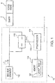
- Fig. 1 a partial view of an exemplary embodiment of a circuit to allow an amplitude and frequency of a sinusoidal voltage waveform to be digitally monitored in accordance with the disclosure is shown in Fig. 1 and is designated generally by reference character 100.
- Other embodiments of such circuits, sensors interfaces employing such circuits, and methods of monitoring amplitude and frequency of sinusoidal voltage waveforms in accordance with the disclosure, or aspects thereof, are provided in Figs. 2-5 , as will be described.
- the systems and methods described herein can be used for monitoring excitation voltages applied to sensors, such as resolvers operably coupled to rotating machinery in aircraft, though the present disclosure is not limited to resolvers or to rotating machinery in general.
- Circuit 100 generally includes an input 101 configured to receive a sinusoidal voltage waveform and an output 103 in operable communication with input 101.
- Output 103 is configured to provide a duty cycle having a nonlinear relationship to the amplitude of the sinusoidal voltage waveform such that an amplitude and frequency of the sinusoidal voltage waveform can be calculated from just the duty cycle.
- circuit 100 is sinusoidal amplitude-to-digital-output (SADO) circuit included in sensor interface 10.
- Sensor interface 10 is connected to a sensor 2 and includes a SADO circuit 100, a sine wave generator 102, a memory 104 with a lookup table 106, and field-programmable-gate-array (FPGA) device or processor 108.
- Sine wave generator 102 is connected to SADO circuit 100 and sensor 2.
- FPGA device or processor 108 is connected to SADO circuit 100 via a digital bus 110 and is disposed in communication with memory 104.
- Lookup table 106 includes an association of sinusoid voltage to amplitude digital output due cycle percentage for an input voltage provided by sine wave generator 102 to SADO circuit 100 and sensor 2.
- Sensor 2 in coupled to a sensed device 4 for determining a parameter of sensed device 4.
- Sensed device 4 is resolver arranged to generate signal indicative of rotational position of rotating machine 6 using an excitation voltage received at sensor 2 by sine wave generator 102. It is to be understood and appreciated that this is for explanation purposes only, and that sensor 2 can be any device employing an excitation voltage with a sinusoidal waveform.
- SADO circuit 100 includes a comparator 112 with an input terminal 114, a reference terminal 116, and an output terminal 118.
- Digital bus 110 is connected to output terminal 118.
- a reference voltage source 120 is connected to reference terminal 116.
- a feedback resistor 122 is connected in parallel between output terminal 118 and input terminal 114 to convert voltage, e.g., sinusoidal voltage shown in Fig. 1 , received at input terminal 114 into a digital pulse-width modulated waveform (shown in Fig. 1 ) that varies non-linearly with amplitude of the voltage received at input terminal 114 (shown in Fig. 4 ).
- SADO circuit 100 include a plurality of discrete electronic components interconnected with one, e.g., resistors and diodes less than fully implemented in silicon.
- SADO circuit 100 also includes a voltage divider circuit 124.
- Voltage divider circuit 124 is connected to input terminal 114 and has a source resistor 126 and a ground resistor 128.
- Source resistor 126 is connected in series between sine wave generator 102 and input terminal 114.
- Ground resistor 128 is connected in series between a ground terminal 129 and input terminal 114.
- a ground lead 131 connects ground resistor 128 to an input lead 130 at a location between source resistor 126 and input terminal 114.
- Voltage divider circuit 124 is arranged, e.g., via respective resistances of source resistor 126 and ground resistor 128, to attenuate voltage of the excitation waveform (shown in Fig. 1 ) applied to input terminal 114.
- SADO circuit 100 additionally includes a half-wave rectifier circuit 132.
- Half-wave rectifier circuit 132 is connected to input terminal 114 and includes a diode 134.
- Diode 134 is connected in series between a ground terminal 129 and input terminal 114, and further connected to input lead 130 at a location between the connection of ground lead 131 and input terminal 114 via a diode lead 138.
- Diode 134 is arranged to oppose current flow from input lead 130, i.e. from input terminal 114 and sine wave generator 102, to ground terminal 136 to half-wave rectify and clamp input voltage received at input terminal 114 to ground.
- diode 134 is a Schottky diode, which provides good efficiency at high switching speeds.
- SADO circuit 100 further includes a hysteresis circuit 140.
- Hysteresis circuit 140 is connected between output terminal 118 and reference terminal 116 and includes a reference resistor 142 and a feedback resistor 144.
- Reference resistor 142 is connected in series between a reference voltage source 146 and reference terminal 116.
- Reference voltage source 146 sets a trip threshold for comparator 112.
- Feedback resistor 144 is connected in parallel with comparator 112, interconnects output terminal 118 with reference terminal 116, and is connected to reference voltage lead 148 at a location between reference terminal 116 and reference resistor 142.
- feedback resistor 144 be arranged to set a width of a hysteresis band (shown in Fig. 3 ) of SADO circuit 100, i.e. a voltage separation 174 (shown in Fig. 3 ) between a low-to-high switching threshold 172 (shown in Fig. 3 ) and a high-to-low switching threshold 170 (shown in Fig. 3 ).
- the width of the hysteresis band is established at least in part based upon resistance of a pull-up resistor 156 connecting a digital bus pull-up voltage source 158 in series to digital bus 110.
- a graph 160 of an input waveform 162 and a digital output waveform 164 are shown. Time is indicated on x-axis 166. Voltage is indicted at y-axis 168.
- Input waveform 162 is provided to SADO circuit 100 (shown in Fig. 1 ) in a sampling arrangement, shown in an exemplary way in Fig. 1 with SADO circuit 100 being connected in parallel with an excitation lead extending between sine wave generator 102 and sensor 2, from sine wave generator 102 (shown in Fig. 1 ).
- SADO circuit 100 converts input waveform 162 into digital output waveform 164, which SADO circuit 100 provides to digital bus 110.
- the above-described circuitry pulse width modulates digital output waveform 164 according to time interval, e.g., the low interval shown in Fig. 3 , between a high-to-low threshold 170 (V H ) and low-to-high threshold 172 (V L ).
- High-to-low threshold 170 (V H ) is greater than low-to-high threshold 172 (V L ), a wide hysteresis band 174 of SADO circuit 100 separating high-to-low threshold 170 (V H ) and low-to-high threshold 172 (V L ).
- SADO circuit 100 compares voltage amplitude of input waveform 162 against high-to-low voltage threshold 170 during intervals when digital output waveform 164 is 'high', e.g., a '1', and further compares the voltage amplitude of input waveform 162 against low-to-high threshold 172 when digital output waveform 164 is 'low', e.g., is a zero.
- High-to-low voltage threshold 170 (V H ) and low-to-high threshold 172 (V L ) are separated in voltage magnitude by a wide hysteresis band 174, which is established by hysteresis circuit 140 (shown in Fig.
- a graph 176 of duty cycle D born by digital output wavefrom 164 (shown in Fig. 3 ) in association with amplitude A of input waveform 162 (shown in Fig. 3 ) is shown.
- Amplitude A is expressed in volts on x-axis 178.
- Duty cycle D is expressed as a percentage on y-axis 180.
- a duty cycle function 182 extends from 0 volts on the left-hand side of graph 176 to about 20 volts on the right-hand side of graph 176, duty cycle function 182 varying in a non-linear with amplitude A.
- duty cycle function 182 allows FPGA device or processor 108 (shown in Fig. 1 ) to calculate both sinusoidal frequency and amplitude using only a single digital input, i.e., digital output waveform 164 (shown in Fig. 3 ).
- Frequency is calculated by measuring time intervals between rising and falling edges of digital output wavefrom 164.
- Amplitude of input waveform 162 is determined by referencing an observed duty cycle (via pulse-width modulation imparted to digital output waveform 164) with an associated amplitdue according to duty cycle function 182.
- a duty cycle of 78% is cross-referenced in lookup table 106 (shown in Fig. 1 ) to recognize that amplitude of input wavefrom 162 is about 6 volts. This amplitude can then be compared against a selected voltage value, or minimum to maximum voltage range (i.e., A MIN to A MAX ), to assess health of input waveform 162.
- Duty cycle function 182 is arrived at via SADO circuitry shown in Fig. 2 as follows.
- output of SADO circuit 100 (shown in Fig. 1 ) is not as accurate as output from a dedicated analog-to-digital converter.
- embodiments of SADO circuit 100 can realize amplitude measurement accuracy of about +/-10% of actual amplitude, which is generally sufficient for sensor interfaces, e.g., sensor interface 10 (shown in Fig. 1 ).
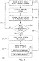
- Method 200 includes generating a digital PWM signal whose duty cycle varies non-linearly with amplitude of the sinusoidal voltage waveform.
- the digital PWM is analyzed, and amplitude and frequency representative of the sinusoidal voltage waveform are calculated using just the digital PWM signal.
- a method of monitoring excitation voltage for a sensor e.g., sensor 2 (shown in Fig. 1 ) is shown. It is to be understood and appreciated that this is for illustration purposes only and is non-limiting.
- Method 200 includes receiving an input voltage with a sinusoidal waveform (shown in Fig. 2 ) at a comparator input terminal, e.g., input terminal 114 (shown in Fig. 2 ), as shown with box 210.
- Method 200 also includes receiving a reference voltage (shown in Fig. 3 ) at a comparator reference terminal, e.g., reference terminal 116 (shown in Fig. 1 ), as shown with box 220. Amplitude of the input voltage is compared to the reference voltage, as shown with box 230. If the input voltage is not greater than the reference voltage then output of the SADO circuit remains the same and monitoring continues, as shown with arrow 250.
- the output of the SADO circuit is toggled between high and low, as shown with arrow 260 and box 270.
- the reference voltage is then offset with the toggled output, as shown with box 280.
- the offsetting can change the reference from a high-to-low threshold to a low-to-high threshold, as shown with box 282.
- the offsetting can change the reference from a low-to-high threshold to a high-to-low threshold, as shown with box 284.
- the magnitude of the reference voltage changes according when the waveform is switched high or low.
- monitoring can continue with output being toggled between high and low according a wide hysteresis defined between the low-to-high and high-to-low thresholds to synthesize a PWM digital output, as shown with arrow 290.
- ADC analog-to-digital converter
- a SADO circuit configured to convert an input voltage varying according to a sinusoidal waveform to a digital pulse-width modulated (PWM) output, the PWM output duty cycle varying nonlinearly with amplitude of the sinusoidal waveform. Varying the PWM output duty cycle nonlinearly with the sinusoidal voltage amplitude allows a microprocessor or a field-programmable gate array (FPGA) to calculate both sinusoidal frequency and amplitude using only a single digital input, i.e., the SADO circuit output. This allows for sinusoidal amplitude and frequency monitoring using digital inputs instead of analog inputs, potentially reducing cost as digital inputs can be more readily implemented than analog inputs.
- PWM digital pulse-width modulated
Landscapes
- Engineering & Computer Science (AREA)
- Theoretical Computer Science (AREA)
- Analogue/Digital Conversion (AREA)
- Measurement Of Current Or Voltage (AREA)
Abstract
Description
- The present disclosure relates to signal conversion, and more particularly to analog to digital signal conversion for analog signal health monitoring.
- Sensors, such as those employed on aircraft, commonly employ excitation voltages to sensors for purposes of monitoring a sensed parameter. For example, in rotating machinery like generators and motors resolvers are commonly employed to sense the rotational position and/or speed of a shaft. Such resolvers generally receive an excitation voltage that varies according to a desired sinusoidal waveform and typically provide an output signal indicative of the rotational position and/or speed of the shaft.
- When providing a sinusoidal voltage excitation waveform it is often desirable to monitor the amplitude of the sinusoidal excitation voltage applied to the sensor. This is because the output of the sensor can change according to variation in the amplitude of the input excitation waveform, potentially changing output of the sensor for a given sensed parameter value. Monitoring the sinusoidal voltage excitation waveform generally involves feeding the sinusoidal signal through an analog-to-digital converter (ADC) device. ADC devices typically have a limited number of input channels, which can limit the number of parameters sensed in certain applications.
- Such conventional methods and systems have generally been considered satisfactory for their intended purpose. However, there is still a need in the art for improved systems and methods for sensor excitation signal monitoring. The present disclosure provides a solution for this need.
- A circuit to allow an amplitude and frequency of a sinusoidal voltage waveform to be digitally monitored includes an input and an output. The input is configured to receive a sinusoidal voltage waveform. The output is in operable communication with the input and is configured to provide a duty cycle having a nonlinear relationship to the amplitude of the sinusoidal voltage waveform such that an amplitude and frequency of the sinusoidal voltage waveform can be calculated from just the duty cycle.
- In certain embodiments, the circuit can be a sinusoidal-amplitude-to-digital-output (SADO). The circuit can include a comparator with an input terminal, a reference terminal and an output terminal. A digital bus can be connected to the output terminal. A reference voltage source can be connected to the reference terminal. A feedback resistor can be connected in parallel with the comparator between the output and input terminals to provide hysteresis for noise rejection such that circuit convert voltage received at the input terminal into a digital pulse-width modulated waveform that varies non-linearly with amplitude of the voltage received at the to the input terminal.
- In accordance with certain embodiments, the SADO circuit can include a plurality of interconnected discrete electronic components. A voltage divider circuit connected to the comparator input terminal to attenuate an input voltage received at the comparator input. A source resistor connected in series between a sine wave generator and the comparator input terminal. A ground resistor can be connected in series between ground and the comparator input terminal.
- In accordance with further embodiments, a half-wave rectifier circuit can be connected to the comparator input terminal to half-wave rectify and clamp the input voltage received at the comparator input terminal to ground. The half-wave rectifier can include a diode connected between ground and the comparator input terminal. The diode can be arranged to oppose current flow from the comparator input terminal and ground.
- It is also contemplated that, in accordance with certain embodiments, a hysteresis circuit. The hysteresis circuit can be connected between the comparator output terminal and the reference voltage terminal. The hysteresis circuit can include a reference resistor connected in series between the reference voltage source and the comparator reference terminal. The feedback resistor can be connected in series between the comparator output terminal and the comparator reference terminal. The feedback resistor can be arranged to set a width of a hysteresis band, i.e., a voltage separation between a low-to-high switching voltage and high-to-low switching voltage, of the comparator. A pull-up resistor can be connected in series between a pull-up voltage source and the comparator output.
- A sensor interface includes a SADO circuit as described above, a sinewave generator connected to the comparator input terminal, and a digital bus connected to the comparator output terminal and the comparator reference terminal. In certain embodiments a field programmable gate array (FPGA) device or a microprocessor can be connected to the comparator output by the digital bus. The FPGA or microprocessor can be disposed in communication with a lookup having input voltage waveform frequency associated with input waveform amplitude.
- A method of monitoring amplitude and frequency of a sinusoidal voltage waveform is shown. The method includes generating a digital pulse-width modulated (PWM) signal whose duty cycle varies non-linearly with amplitude of the sinusoidal voltage waveform. The digital PWM is analyzed, and amplitude and frequency representative of the sinusoidal voltage waveform are calculated using just the digital PWM signal.
- In certain embodiments the method can be a method on monitoring excitation voltage for a sensor. An input voltage with a sinusoidal waveform can be received at a comparator input terminal and a reference voltage at a comparator reference terminal. An output voltage can be received at a comparator output terminal and switched from a first to a second voltage when amplitude of the input voltage rises above a low-to-high threshold. The output voltage can be switched from the second to the first voltage when amplitude of the input voltage drops below a low-to-high threshold.
- In accordance with certain embodiments the low-to-high threshold can be less than the high-to-low threshold. The low-to-high threshold can be generated by offsetting the reference voltage by the first voltage after switching from the second to the first voltage. The high-to-low threshold can be generated by offsetting the reference voltage by the output voltage after switching from the first to the second voltage.
- These and other features of the systems and methods of the subject disclosure will become more readily apparent to those skilled in the art from the following detailed description of the preferred embodiments taken in conjunction with the drawings.
- So that those skilled in the art to which the subject disclosure appertains will readily understand how to make and use the devices and methods of the subject disclosure without undue experimentation, embodiments thereof will be described in detail herein below with reference to certain figures, wherein:
-
Fig. 1 is a schematic view of an exemplary embodiment sensor interface with a sinusoidal-amplitude-to-digital-output (SADO) circuit constructed in accordance with the present disclosure, showing the sensor interface connected between a sine wave generator and a sensor; -
Fig. 2 is a circuit diagram of the sensor interface ofFig. 1 , showing discrete electronic components of the SADO circuit interconnected with one another; and -
Figs. 3 and 4 are graphs of output of the SADO circuit ofFig. 1 , showing digital output duty cycle percentage as a function of input voltage amplitude and digital output for an exemplary waveform, respectively; and -
Fig. 5 is a process flow diagram for a method of converting a sinusoidal waveform into a pulse-width modulated output waveform, showing steps of the method. - Reference will now be made to the drawings wherein like reference numerals identify similar structural features or aspects of the subject disclosure. For purposes of explanation and illustration, and not limitation, a partial view of an exemplary embodiment of a circuit to allow an amplitude and frequency of a sinusoidal voltage waveform to be digitally monitored in accordance with the disclosure is shown in
Fig. 1 and is designated generally byreference character 100. Other embodiments of such circuits, sensors interfaces employing such circuits, and methods of monitoring amplitude and frequency of sinusoidal voltage waveforms in accordance with the disclosure, or aspects thereof, are provided inFigs. 2-5 , as will be described. The systems and methods described herein can be used for monitoring excitation voltages applied to sensors, such as resolvers operably coupled to rotating machinery in aircraft, though the present disclosure is not limited to resolvers or to rotating machinery in general. - Referring to
Fig. 1 ,circuit 100 is shown.Circuit 100 generally includes aninput 101 configured to receive a sinusoidal voltage waveform and anoutput 103 in operable communication withinput 101.Output 103 is configured to provide a duty cycle having a nonlinear relationship to the amplitude of the sinusoidal voltage waveform such that an amplitude and frequency of the sinusoidal voltage waveform can be calculated from just the duty cycle. - In the illustrated
exemplary embodiment circuit 100 is sinusoidal amplitude-to-digital-output (SADO) circuit included insensor interface 10.Sensor interface 10 is connected to asensor 2 and includes aSADO circuit 100, asine wave generator 102, amemory 104 with a lookup table 106, and field-programmable-gate-array (FPGA) device orprocessor 108.Sine wave generator 102 is connected to SADOcircuit 100 andsensor 2. FPGA device orprocessor 108 is connected to SADOcircuit 100 via adigital bus 110 and is disposed in communication withmemory 104. Lookup table 106 includes an association of sinusoid voltage to amplitude digital output due cycle percentage for an input voltage provided bysine wave generator 102 toSADO circuit 100 andsensor 2.Sensor 2 in coupled to a senseddevice 4 for determining a parameter of senseddevice 4. Senseddevice 4 is resolver arranged to generate signal indicative of rotational position of rotating machine 6 using an excitation voltage received atsensor 2 bysine wave generator 102. It is to be understood and appreciated that this is for explanation purposes only, and thatsensor 2 can be any device employing an excitation voltage with a sinusoidal waveform. - With reference to
Fig. 2 , a circuit diagram ofSADO circuit 100 is shown. SADOcircuit 100 includes acomparator 112 with aninput terminal 114, areference terminal 116, and anoutput terminal 118.Digital bus 110 is connected tooutput terminal 118. A reference voltage source 120 is connected toreference terminal 116. A feedback resistor 122 is connected in parallel betweenoutput terminal 118 andinput terminal 114 to convert voltage, e.g., sinusoidal voltage shown inFig. 1 , received atinput terminal 114 into a digital pulse-width modulated waveform (shown inFig. 1 ) that varies non-linearly with amplitude of the voltage received at input terminal 114 (shown inFig. 4 ). It is contemplated thatSADO circuit 100 include a plurality of discrete electronic components interconnected with one, e.g., resistors and diodes less than fully implemented in silicon. - SADO
circuit 100 also includes avoltage divider circuit 124.Voltage divider circuit 124 is connected to input terminal 114 and has asource resistor 126 and aground resistor 128.Source resistor 126 is connected in series betweensine wave generator 102 andinput terminal 114.Ground resistor 128 is connected in series between aground terminal 129 andinput terminal 114. A ground lead 131 connectsground resistor 128 to aninput lead 130 at a location betweensource resistor 126 andinput terminal 114.Voltage divider circuit 124 is arranged, e.g., via respective resistances ofsource resistor 126 andground resistor 128, to attenuate voltage of the excitation waveform (shown inFig. 1 ) applied to input terminal 114. - SADO
circuit 100 additionally includes a half-wave rectifier circuit 132. Half-wave rectifier circuit 132 is connected to input terminal 114 and includes adiode 134.Diode 134 is connected in series between aground terminal 129 andinput terminal 114, and further connected to input lead 130 at a location between the connection of ground lead 131 andinput terminal 114 via adiode lead 138.Diode 134 is arranged to oppose current flow frominput lead 130, i.e. frominput terminal 114 andsine wave generator 102, to ground terminal 136 to half-wave rectify and clamp input voltage received atinput terminal 114 to ground. In the illustratedexemplary embodiment diode 134 is a Schottky diode, which provides good efficiency at high switching speeds. - SADO
circuit 100 further includes ahysteresis circuit 140.Hysteresis circuit 140 is connected betweenoutput terminal 118 andreference terminal 116 and includes areference resistor 142 and afeedback resistor 144.Reference resistor 142 is connected in series between areference voltage source 146 andreference terminal 116.Reference voltage source 146 sets a trip threshold forcomparator 112.Feedback resistor 144 is connected in parallel withcomparator 112, interconnectsoutput terminal 118 withreference terminal 116, and is connected to referencevoltage lead 148 at a location betweenreference terminal 116 andreference resistor 142. - It is contemplated that
feedback resistor 144 be arranged to set a width of a hysteresis band (shown inFig. 3 ) of SADOcircuit 100, i.e. a voltage separation 174 (shown inFig. 3 ) between a low-to-high switching threshold 172 (shown inFig. 3 ) and a high-to-low switching threshold 170 (shown inFig. 3 ). The width of the hysteresis band is established at least in part based upon resistance of a pull-upresistor 156 connecting a digital bus pull-upvoltage source 158 in series todigital bus 110. - With reference to
Fig. 3 , agraph 160 of aninput waveform 162 and adigital output waveform 164 are shown. Time is indicated onx-axis 166. Voltage is indicted at y-axis 168.Input waveform 162 is provided to SADO circuit 100 (shown inFig. 1 ) in a sampling arrangement, shown in an exemplary way inFig. 1 with SADOcircuit 100 being connected in parallel with an excitation lead extending betweensine wave generator 102 andsensor 2, from sine wave generator 102 (shown inFig. 1 ). - As
input waveform 162 arrives SADOcircuit 100 convertsinput waveform 162 intodigital output waveform 164, which SADOcircuit 100 provides todigital bus 110. The above-described circuitry pulse width modulatesdigital output waveform 164 according to time interval, e.g., the low interval shown inFig. 3 , between a high-to-low threshold 170 (VH) and low-to-high threshold 172 (VL). High-to-low threshold 170 (VH) is greater than low-to-high threshold 172 (VL), awide hysteresis band 174 ofSADO circuit 100 separating high-to-low threshold 170 (VH) and low-to-high threshold 172 (VL). - SADO
circuit 100 compares voltage amplitude ofinput waveform 162 against high-to-low voltage threshold 170 during intervals whendigital output waveform 164 is 'high', e.g., a '1', and further compares the voltage amplitude ofinput waveform 162 against low-to-high threshold 172 whendigital output waveform 164 is 'low', e.g., is a zero. High-to-low voltage threshold 170 (VH) and low-to-high threshold 172 (VL) are separated in voltage magnitude by awide hysteresis band 174, which is established by hysteresis circuit 140 (shown inFig. 2 ) and operates to switch the reference voltage applied to reference terminal 116 (shown inFig. 2 ) according to whetherdigital output waveform 164 is high or low. The proportion of time during which thedigital output waveform 164 is high corresponds to the duty cycle modulated intodigital output waveform 164, which is provided in real-time to FPGA device orprocessor 108 for determining health ofinput waveform 162. - With reference to
Fig. 4 , agraph 176 of duty cycle D born by digital output wavefrom 164 (shown inFig. 3 ) in association with amplitude A of input waveform 162 (shown inFig. 3 ) is shown. Amplitude A is expressed in volts onx-axis 178. Duty cycle D is expressed as a percentage on y-axis 180. Aduty cycle function 182 extends from 0 volts on the left-hand side ofgraph 176 to about 20 volts on the right-hand side ofgraph 176,duty cycle function 182 varying in a non-linear with amplitude A. As will be appreciated by those of skill in art in view of the present disclosure, the non-linearity ofduty cycle function 182 allows FPGA device or processor 108 (shown inFig. 1 ) to calculate both sinusoidal frequency and amplitude using only a single digital input, i.e., digital output waveform 164 (shown inFig. 3 ). - Frequency is calculated by measuring time intervals between rising and falling edges of
digital output wavefrom 164. Amplitude ofinput waveform 162 is determined by referencing an observed duty cycle (via pulse-width modulation imparted to digital output waveform 164) with an associated amplitdue according toduty cycle function 182. In an exemplary implementation shown inFig. 4 , a duty cycle of 78% is cross-referenced in lookup table 106 (shown inFig. 1 ) to recognize that amplitude ofinput wavefrom 162 is about 6 volts. This amplitude can then be compared against a selected voltage value, or minimum to maximum voltage range (i.e., AMIN to AMAX), to assess health ofinput waveform 162. -
Duty cycle function 182 is arrived at via SADO circuitry shown inFig. 2 as follows. Input waveform 162 a sinusoidal waveform with amplitude A and an angular frequency ω, and generally conforms to Equation 1:
Fig. 2 ) has a high-to-low threshold VH and a low-to-high threshold VL, then the time associated withinput waveform 160 crossing high-to-low threshold VH is according to Equation 2: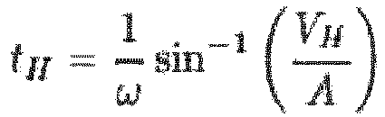
input waveform 162 crossing low-to-high threshold VL is according to Equation 3: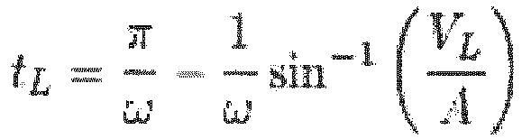

Substituting Equation 2 and Equation 3 intoEquation 4, and accounting for the constraint imposed by the dome of the arcsine yields an expression that is independent of angular frequency according to Equation 5:
Fig. 4 withduty cycle function 182. - In certain embodiments, output of SADO circuit 100 (shown in
Fig. 1 ) is not as accurate as output from a dedicated analog-to-digital converter. However, using discrete components, embodiments ofSADO circuit 100 can realize amplitude measurement accuracy of about +/-10% of actual amplitude, which is generally sufficient for sensor interfaces, e.g., sensor interface 10 (shown inFig. 1 ). - With reference to
Fig. 5 , amethod 200 of monitoring amplitude and frequency of a sinusoidal voltage waveform is shown.Method 200 includes generating a digital PWM signal whose duty cycle varies non-linearly with amplitude of the sinusoidal voltage waveform. The digital PWM is analyzed, and amplitude and frequency representative of the sinusoidal voltage waveform are calculated using just the digital PWM signal. In the illustrated exemplary embodiment a method of monitoring excitation voltage for a sensor, e.g., sensor 2 (shown inFig. 1 ) is shown. It is to be understood and appreciated that this is for illustration purposes only and is non-limiting. -
Method 200 includes receiving an input voltage with a sinusoidal waveform (shown inFig. 2 ) at a comparator input terminal, e.g., input terminal 114 (shown inFig. 2 ), as shown withbox 210.Method 200 also includes receiving a reference voltage (shown inFig. 3 ) at a comparator reference terminal, e.g., reference terminal 116 (shown inFig. 1 ), as shown withbox 220. Amplitude of the input voltage is compared to the reference voltage, as shown withbox 230. If the input voltage is not greater than the reference voltage then output of the SADO circuit remains the same and monitoring continues, as shown witharrow 250. - When the comparison indicates that the input voltage is greater than the reference voltage then the output of the SADO circuit is toggled between high and low, as shown with
arrow 260 andbox 270. The reference voltage is then offset with the toggled output, as shown withbox 280. The offsetting can change the reference from a high-to-low threshold to a low-to-high threshold, as shown withbox 282. The offsetting can change the reference from a low-to-high threshold to a high-to-low threshold, as shown withbox 284. The magnitude of the reference voltage changes according when the waveform is switched high or low. It is contemplated that monitoring can continue with output being toggled between high and low according a wide hysteresis defined between the low-to-high and high-to-low thresholds to synthesize a PWM digital output, as shown witharrow 290. - When providing a sinusoidal voltage excitation waveform it can be desirable to monitor amplitude of the sinusoid. Usually this involves feeding the sinusoid back through an analog-to-digital converter (ADC). While generally satisfactory for its intended purpose, the number of ADC channels available in a given application may be such that no monitoring channel is available to receive the sinusoidal waveform.
- In embodiments described herein a SADO circuit is provided. The SADO circuit is configured to convert an input voltage varying according to a sinusoidal waveform to a digital pulse-width modulated (PWM) output, the PWM output duty cycle varying nonlinearly with amplitude of the sinusoidal waveform. Varying the PWM output duty cycle nonlinearly with the sinusoidal voltage amplitude allows a microprocessor or a field-programmable gate array (FPGA) to calculate both sinusoidal frequency and amplitude using only a single digital input, i.e., the SADO circuit output. This allows for sinusoidal amplitude and frequency monitoring using digital inputs instead of analog inputs, potentially reducing cost as digital inputs can be more readily implemented than analog inputs.
- The methods and systems of the present disclosure, as described above and shown in the drawings, provide for sensor interfaces with superior properties including the sinusoidal excitation voltage waveform amplitude and frequency monitoring with the use of an ADC. While the apparatus and methods of the subject disclosure have been shown and described with reference to preferred embodiments, those skilled in the art will readily appreciate that changes and/or modifications may be made thereto without departing from the scope of the subject disclosure.
Claims (15)
- A circuit to allow an amplitude and frequency of a sinusoidal voltage waveform to be digitally monitored, comprising:an input (101) configured to receive the sinusoidal voltage waveform; andan output (103) in operable communication with the input configured to provide a duty cycle having a nonlinear relationship to the amplitude of the sinusoidal voltage waveform such that an amplitude and frequency of the sinusoidal voltage waveform can be calculated from just the duty cycle.
- The circuit as recited in claim 1, wherein circuit is a sinusoidal-amplitude-to-digital-output (SADO) circuit (100), wherein the input and output comprise:a comparator (112) with an input terminal (114), a reference terminal (116), and an output terminal (118);a digital bus (110) connected to the output terminal;a reference voltage source (120) connected to the reference terminal; anda feedback resistor (122) connected in parallel between the output terminal and the input terminal to convert an input voltage received at the input terminal into a digital pulse-width modulated (PWM) waveform that varies non-linearly with amplitude of the input voltage.
- The circuit as recited in claim 2, further comprising a voltage divider circuit (124) connected to the comparator input terminal to attenuate the input voltage; and/or further comprising a half-wave rectifier circuit (130) connected to the comparator input circuit to half-wave rectify and clamp the input voltage.
- The circuit as recited in claim 2 or 3, further comprising a resistor connected in series between the reference voltage source and the comparator reference terminal.
- The circuit as recited in claim 2, 3 or 4, further comprising a pull-up resistor connected in series between the digital bus and a digital bus voltage source.
- The circuit as recited in any of claims 2 to 5, wherein output of the circuit has an output duty cycle according to:

- A sensor interface, comprising:a circuit as recited in any of claims 2 to 6;a sine wave generator (102) connected to the input terminal of the comparator; anda digital bus (110) connected to the output terminal and the reference terminal of the comparator.
- The sensor interface as recited in claim 7, further comprising a field programmable gate array (FPGA) (108) or microprocessor device connected to the digital bus and configured to calculate both frequency and amplitude of a waveform of the input voltage using the PWM waveform received at the comparator output terminal.
- The sensor interface as recited in claim 8, further comprising a lookup table (106) accessible by the FPGA or microprocessor device with voltage amplitude associated with duty cycle.
- A method of monitoring amplitude and frequency of a sinusoidal voltage waveform comprising:generating a digital pulse width modulation (PWM) signal whose duty cycle varies nonlinearly with an amplitude of the sinusoidal voltage waveform;analyzing the digital PWM signal; andcalculating, using the just the digital PWM signal, an amplitude and frequency representative of the sinusoidal voltage waveform.
- The method as recited in claim 10, wherein the sinusoidal waveform is an excitation voltage for a sensor.
- The method as recited in claim 10 or 11, further comprising:receiving an input voltage with a sinusoidal waveform at a comparator input terminal;receiving a reference voltage at a comparator reference terminal;switching an output voltage applied at a comparator output terminal from a first voltage to a second voltage when amplitude of the input voltage crosses a low-to-high threshold; andswitching the output voltage applied at the comparator output terminal from the second voltage to the first voltage when amplitude of the input voltage crosses a high-to-low threshold.
- The method as recited in claim 12, wherein the high-to-low threshold is greater than the low-to-high threshold.
- The method as recited in claim 12 or 13, further comprising generating the low-to-high threshold by offsetting the reference voltage by the first voltage subsequent to switching from the second voltage to the first voltage.
- The method as recited in claim 12, 13 or 14, further comprising generating the high-to-low threshold by offsetting the reference voltage offset by the second voltage subsequent to switching from the first voltage to the second voltage.
Applications Claiming Priority (1)
| Application Number | Priority Date | Filing Date | Title |
|---|---|---|---|
| US15/487,055 US9960784B1 (en) | 2017-04-13 | 2017-04-13 | Analog to digital converters |
Publications (2)
| Publication Number | Publication Date |
|---|---|
| EP3389188A1 true EP3389188A1 (en) | 2018-10-17 |
| EP3389188B1 EP3389188B1 (en) | 2022-07-20 |
Family
ID=62013823
Family Applications (1)
| Application Number | Title | Priority Date | Filing Date |
|---|---|---|---|
| EP18167344.3A Active EP3389188B1 (en) | 2017-04-13 | 2018-04-13 | Analog to digital converters |
Country Status (2)
| Country | Link |
|---|---|
| US (1) | US9960784B1 (en) |
| EP (1) | EP3389188B1 (en) |
Citations (5)
| Publication number | Priority date | Publication date | Assignee | Title |
|---|---|---|---|---|
| US5218315A (en) * | 1992-01-06 | 1993-06-08 | Infinity Systems, Inc. | Switching amplifier |
| WO2011149866A2 (en) * | 2010-05-27 | 2011-12-01 | Osram Sylvania Inc. | Dimmer conduction angle detection circuit and system incorporating the same |
| US20130051092A1 (en) * | 2011-08-25 | 2013-02-28 | Direct Grid Technologies LLC | Apparatus for a microinverter particularly suited for use in solar power installations |
| EP3015872A1 (en) * | 2014-10-30 | 2016-05-04 | DET International Holding Limited | Threshold detection circuit |
| US20160248381A1 (en) * | 2013-10-23 | 2016-08-25 | Samsung Electronics Co., Ltd. | Power amplification device and method |
Family Cites Families (6)
| Publication number | Priority date | Publication date | Assignee | Title |
|---|---|---|---|---|
| US3789393A (en) | 1972-10-26 | 1974-01-29 | Inductosyn Corp | Digital/analog converter with amplitude and pulse-width modulation |
| US6567922B1 (en) | 2000-04-21 | 2003-05-20 | Hsiu-Mei Feng | Pulse type activating system for power supply |
| US7205916B1 (en) * | 2006-01-27 | 2007-04-17 | Alliant Techsystems Inc. | Digital method and apparatus for resolving shaft position |
| US7248994B1 (en) * | 2006-01-27 | 2007-07-24 | Alliant Techsystems Inc. | Digital method and apparatus for sensing position with a linear variable differential transformer |
| US7696791B2 (en) | 2007-12-31 | 2010-04-13 | Intel Corporation | High-speed amplitude detector with a digital output |
| US9059641B2 (en) | 2011-07-05 | 2015-06-16 | Atmel Corporation | Main supply zero crossing detection for PFC converter |
-
2017
- 2017-04-13 US US15/487,055 patent/US9960784B1/en active Active
-
2018
- 2018-04-13 EP EP18167344.3A patent/EP3389188B1/en active Active
Patent Citations (5)
| Publication number | Priority date | Publication date | Assignee | Title |
|---|---|---|---|---|
| US5218315A (en) * | 1992-01-06 | 1993-06-08 | Infinity Systems, Inc. | Switching amplifier |
| WO2011149866A2 (en) * | 2010-05-27 | 2011-12-01 | Osram Sylvania Inc. | Dimmer conduction angle detection circuit and system incorporating the same |
| US20130051092A1 (en) * | 2011-08-25 | 2013-02-28 | Direct Grid Technologies LLC | Apparatus for a microinverter particularly suited for use in solar power installations |
| US20160248381A1 (en) * | 2013-10-23 | 2016-08-25 | Samsung Electronics Co., Ltd. | Power amplification device and method |
| EP3015872A1 (en) * | 2014-10-30 | 2016-05-04 | DET International Holding Limited | Threshold detection circuit |
Also Published As
| Publication number | Publication date |
|---|---|
| US9960784B1 (en) | 2018-05-01 |
| EP3389188B1 (en) | 2022-07-20 |
Similar Documents
| Publication | Publication Date | Title |
|---|---|---|
| US8035528B2 (en) | Fast detection of contact status with AC wetting voltage using ratiometric approach | |
| US8587974B2 (en) | Method and device for increasing control accuracy in a PWM system | |
| US20160065087A1 (en) | Current detecting circuit for power element | |
| KR102019384B1 (en) | Resolver management device, resolver system having the same, and operating method thereof | |
| CN104704376B (en) | Method and apparatus for measuring the electric current by switch | |
| EP3540936A1 (en) | Motor control apparatus, motor control program, and motor control method | |
| US10644635B2 (en) | Systems and methods for motor drive cable characteristics identification and compensation therefor | |
| JP2016166770A (en) | Electric leak detection device | |
| US10615736B2 (en) | Temperature monitoring | |
| EP3389188B1 (en) | Analog to digital converters | |
| EP0562452B1 (en) | An interface circuit for generating an analogue signal to control the speed of rotation of a direct-current electric motor, particularly a brushless motor | |
| EP0058050A1 (en) | Measuring method | |
| CN102204106B (en) | Power conversion device | |
| US11536616B2 (en) | Sensor device and method for operating a sensor device | |
| GB2524386A (en) | Method and apparatus for detecting a short circuit on a PWM driver circuit | |
| CN105391320A (en) | Multi-phase power circuit | |
| US9653971B2 (en) | Speed detection circuits for permanent magnet alternators | |
| US20080164958A1 (en) | Method and apparatus for pulse width modulation | |
| EP3041119A2 (en) | Digital frequency selective transformer-rectifier unit ripple fault detection | |
| WO2023006337A1 (en) | Circuit arrangement, electrical system and method for determining depletion layer temperatures of gate-controlled semiconductor components | |
| CN110945330B (en) | Temperature sensor circuit | |
| Senicar et al. | Inverter based method for measurement of PMSM machine parameters based on the elimination of power stage characteristics | |
| DE102004038564B4 (en) | Circuit and method for detecting a temperature and device | |
| JP7019864B1 (en) | State estimation system and state estimation method for power conversion semiconductor devices | |
| US20250379526A1 (en) | High accuracy power conversion system having multiplex pin and control circuit and method thereof |
Legal Events
| Date | Code | Title | Description |
|---|---|---|---|
| PUAI | Public reference made under article 153(3) epc to a published international application that has entered the european phase |
Free format text: ORIGINAL CODE: 0009012 |
|
| STAA | Information on the status of an ep patent application or granted ep patent |
Free format text: STATUS: THE APPLICATION HAS BEEN PUBLISHED |
|
| AK | Designated contracting states |
Kind code of ref document: A1 Designated state(s): AL AT BE BG CH CY CZ DE DK EE ES FI FR GB GR HR HU IE IS IT LI LT LU LV MC MK MT NL NO PL PT RO RS SE SI SK SM TR |
|
| AX | Request for extension of the european patent |
Extension state: BA ME |
|
| STAA | Information on the status of an ep patent application or granted ep patent |
Free format text: STATUS: REQUEST FOR EXAMINATION WAS MADE |
|
| 17P | Request for examination filed |
Effective date: 20190416 |
|
| RBV | Designated contracting states (corrected) |
Designated state(s): AL AT BE BG CH CY CZ DE DK EE ES FI FR GB GR HR HU IE IS IT LI LT LU LV MC MK MT NL NO PL PT RO RS SE SI SK SM TR |
|
| STAA | Information on the status of an ep patent application or granted ep patent |
Free format text: STATUS: EXAMINATION IS IN PROGRESS |
|
| 17Q | First examination report despatched |
Effective date: 20200403 |
|
| RIC1 | Information provided on ipc code assigned before grant |
Ipc: H03M 1/48 20060101ALN20211223BHEP Ipc: H03K 7/08 20060101ALI20211223BHEP Ipc: H03M 1/34 20060101ALI20211223BHEP Ipc: H03M 1/50 20060101AFI20211223BHEP |
|
| GRAP | Despatch of communication of intention to grant a patent |
Free format text: ORIGINAL CODE: EPIDOSNIGR1 |
|
| STAA | Information on the status of an ep patent application or granted ep patent |
Free format text: STATUS: GRANT OF PATENT IS INTENDED |
|
| RIC1 | Information provided on ipc code assigned before grant |
Ipc: H03M 1/48 20060101ALN20220126BHEP Ipc: H03K 7/08 20060101ALI20220126BHEP Ipc: H03M 1/34 20060101ALI20220126BHEP Ipc: H03M 1/50 20060101AFI20220126BHEP |
|
| INTG | Intention to grant announced |
Effective date: 20220214 |
|
| GRAS | Grant fee paid |
Free format text: ORIGINAL CODE: EPIDOSNIGR3 |
|
| GRAA | (expected) grant |
Free format text: ORIGINAL CODE: 0009210 |
|
| STAA | Information on the status of an ep patent application or granted ep patent |
Free format text: STATUS: THE PATENT HAS BEEN GRANTED |
|
| AK | Designated contracting states |
Kind code of ref document: B1 Designated state(s): AL AT BE BG CH CY CZ DE DK EE ES FI FR GB GR HR HU IE IS IT LI LT LU LV MC MK MT NL NO PL PT RO RS SE SI SK SM TR |
|
| REG | Reference to a national code |
Ref country code: CH Ref legal event code: EP |
|
| REG | Reference to a national code |
Ref country code: DE Ref legal event code: R096 Ref document number: 602018038042 Country of ref document: DE |
|
| REG | Reference to a national code |
Ref country code: AT Ref legal event code: REF Ref document number: 1506219 Country of ref document: AT Kind code of ref document: T Effective date: 20220815 |
|
| REG | Reference to a national code |
Ref country code: IE Ref legal event code: FG4D |
|
| REG | Reference to a national code |
Ref country code: LT Ref legal event code: MG9D |
|
| REG | Reference to a national code |
Ref country code: NL Ref legal event code: MP Effective date: 20220720 |
|
| PG25 | Lapsed in a contracting state [announced via postgrant information from national office to epo] |
Ref country code: SE Free format text: LAPSE BECAUSE OF FAILURE TO SUBMIT A TRANSLATION OF THE DESCRIPTION OR TO PAY THE FEE WITHIN THE PRESCRIBED TIME-LIMIT Effective date: 20220720 Ref country code: RS Free format text: LAPSE BECAUSE OF FAILURE TO SUBMIT A TRANSLATION OF THE DESCRIPTION OR TO PAY THE FEE WITHIN THE PRESCRIBED TIME-LIMIT Effective date: 20220720 Ref country code: PT Free format text: LAPSE BECAUSE OF FAILURE TO SUBMIT A TRANSLATION OF THE DESCRIPTION OR TO PAY THE FEE WITHIN THE PRESCRIBED TIME-LIMIT Effective date: 20221121 Ref country code: NO Free format text: LAPSE BECAUSE OF FAILURE TO SUBMIT A TRANSLATION OF THE DESCRIPTION OR TO PAY THE FEE WITHIN THE PRESCRIBED TIME-LIMIT Effective date: 20221020 Ref country code: NL Free format text: LAPSE BECAUSE OF FAILURE TO SUBMIT A TRANSLATION OF THE DESCRIPTION OR TO PAY THE FEE WITHIN THE PRESCRIBED TIME-LIMIT Effective date: 20220720 Ref country code: LV Free format text: LAPSE BECAUSE OF FAILURE TO SUBMIT A TRANSLATION OF THE DESCRIPTION OR TO PAY THE FEE WITHIN THE PRESCRIBED TIME-LIMIT Effective date: 20220720 Ref country code: LT Free format text: LAPSE BECAUSE OF FAILURE TO SUBMIT A TRANSLATION OF THE DESCRIPTION OR TO PAY THE FEE WITHIN THE PRESCRIBED TIME-LIMIT Effective date: 20220720 Ref country code: FI Free format text: LAPSE BECAUSE OF FAILURE TO SUBMIT A TRANSLATION OF THE DESCRIPTION OR TO PAY THE FEE WITHIN THE PRESCRIBED TIME-LIMIT Effective date: 20220720 Ref country code: ES Free format text: LAPSE BECAUSE OF FAILURE TO SUBMIT A TRANSLATION OF THE DESCRIPTION OR TO PAY THE FEE WITHIN THE PRESCRIBED TIME-LIMIT Effective date: 20220720 |
|
| REG | Reference to a national code |
Ref country code: AT Ref legal event code: MK05 Ref document number: 1506219 Country of ref document: AT Kind code of ref document: T Effective date: 20220720 |
|
| PG25 | Lapsed in a contracting state [announced via postgrant information from national office to epo] |
Ref country code: PL Free format text: LAPSE BECAUSE OF FAILURE TO SUBMIT A TRANSLATION OF THE DESCRIPTION OR TO PAY THE FEE WITHIN THE PRESCRIBED TIME-LIMIT Effective date: 20220720 Ref country code: IS Free format text: LAPSE BECAUSE OF FAILURE TO SUBMIT A TRANSLATION OF THE DESCRIPTION OR TO PAY THE FEE WITHIN THE PRESCRIBED TIME-LIMIT Effective date: 20221120 Ref country code: HR Free format text: LAPSE BECAUSE OF FAILURE TO SUBMIT A TRANSLATION OF THE DESCRIPTION OR TO PAY THE FEE WITHIN THE PRESCRIBED TIME-LIMIT Effective date: 20220720 Ref country code: GR Free format text: LAPSE BECAUSE OF FAILURE TO SUBMIT A TRANSLATION OF THE DESCRIPTION OR TO PAY THE FEE WITHIN THE PRESCRIBED TIME-LIMIT Effective date: 20221021 |
|
| REG | Reference to a national code |
Ref country code: DE Ref legal event code: R097 Ref document number: 602018038042 Country of ref document: DE |
|
| PG25 | Lapsed in a contracting state [announced via postgrant information from national office to epo] |
Ref country code: SM Free format text: LAPSE BECAUSE OF FAILURE TO SUBMIT A TRANSLATION OF THE DESCRIPTION OR TO PAY THE FEE WITHIN THE PRESCRIBED TIME-LIMIT Effective date: 20220720 Ref country code: RO Free format text: LAPSE BECAUSE OF FAILURE TO SUBMIT A TRANSLATION OF THE DESCRIPTION OR TO PAY THE FEE WITHIN THE PRESCRIBED TIME-LIMIT Effective date: 20220720 Ref country code: DK Free format text: LAPSE BECAUSE OF FAILURE TO SUBMIT A TRANSLATION OF THE DESCRIPTION OR TO PAY THE FEE WITHIN THE PRESCRIBED TIME-LIMIT Effective date: 20220720 Ref country code: CZ Free format text: LAPSE BECAUSE OF FAILURE TO SUBMIT A TRANSLATION OF THE DESCRIPTION OR TO PAY THE FEE WITHIN THE PRESCRIBED TIME-LIMIT Effective date: 20220720 Ref country code: AT Free format text: LAPSE BECAUSE OF FAILURE TO SUBMIT A TRANSLATION OF THE DESCRIPTION OR TO PAY THE FEE WITHIN THE PRESCRIBED TIME-LIMIT Effective date: 20220720 |
|
| PLBE | No opposition filed within time limit |
Free format text: ORIGINAL CODE: 0009261 |
|
| STAA | Information on the status of an ep patent application or granted ep patent |
Free format text: STATUS: NO OPPOSITION FILED WITHIN TIME LIMIT |
|
| PG25 | Lapsed in a contracting state [announced via postgrant information from national office to epo] |
Ref country code: SK Free format text: LAPSE BECAUSE OF FAILURE TO SUBMIT A TRANSLATION OF THE DESCRIPTION OR TO PAY THE FEE WITHIN THE PRESCRIBED TIME-LIMIT Effective date: 20220720 Ref country code: EE Free format text: LAPSE BECAUSE OF FAILURE TO SUBMIT A TRANSLATION OF THE DESCRIPTION OR TO PAY THE FEE WITHIN THE PRESCRIBED TIME-LIMIT Effective date: 20220720 |
|
| 26N | No opposition filed |
Effective date: 20230421 |
|
| P01 | Opt-out of the competence of the unified patent court (upc) registered |
Effective date: 20230522 |
|
| PG25 | Lapsed in a contracting state [announced via postgrant information from national office to epo] |
Ref country code: AL Free format text: LAPSE BECAUSE OF FAILURE TO SUBMIT A TRANSLATION OF THE DESCRIPTION OR TO PAY THE FEE WITHIN THE PRESCRIBED TIME-LIMIT Effective date: 20220720 |
|
| PG25 | Lapsed in a contracting state [announced via postgrant information from national office to epo] |
Ref country code: SI Free format text: LAPSE BECAUSE OF FAILURE TO SUBMIT A TRANSLATION OF THE DESCRIPTION OR TO PAY THE FEE WITHIN THE PRESCRIBED TIME-LIMIT Effective date: 20220720 |
|
| REG | Reference to a national code |
Ref country code: CH Ref legal event code: PL |
|
| PG25 | Lapsed in a contracting state [announced via postgrant information from national office to epo] |
Ref country code: LU Free format text: LAPSE BECAUSE OF NON-PAYMENT OF DUE FEES Effective date: 20230413 |
|
| REG | Reference to a national code |
Ref country code: BE Ref legal event code: MM Effective date: 20230430 |
|
| PG25 | Lapsed in a contracting state [announced via postgrant information from national office to epo] |
Ref country code: MC Free format text: LAPSE BECAUSE OF FAILURE TO SUBMIT A TRANSLATION OF THE DESCRIPTION OR TO PAY THE FEE WITHIN THE PRESCRIBED TIME-LIMIT Effective date: 20220720 |
|
| PG25 | Lapsed in a contracting state [announced via postgrant information from national office to epo] |
Ref country code: MC Free format text: LAPSE BECAUSE OF FAILURE TO SUBMIT A TRANSLATION OF THE DESCRIPTION OR TO PAY THE FEE WITHIN THE PRESCRIBED TIME-LIMIT Effective date: 20220720 Ref country code: LI Free format text: LAPSE BECAUSE OF NON-PAYMENT OF DUE FEES Effective date: 20230430 Ref country code: CH Free format text: LAPSE BECAUSE OF NON-PAYMENT OF DUE FEES Effective date: 20230430 |
|
| REG | Reference to a national code |
Ref country code: IE Ref legal event code: MM4A |
|
| PG25 | Lapsed in a contracting state [announced via postgrant information from national office to epo] |
Ref country code: BE Free format text: LAPSE BECAUSE OF NON-PAYMENT OF DUE FEES Effective date: 20230430 |
|
| PG25 | Lapsed in a contracting state [announced via postgrant information from national office to epo] |
Ref country code: IE Free format text: LAPSE BECAUSE OF NON-PAYMENT OF DUE FEES Effective date: 20230413 |
|
| PG25 | Lapsed in a contracting state [announced via postgrant information from national office to epo] |
Ref country code: IE Free format text: LAPSE BECAUSE OF NON-PAYMENT OF DUE FEES Effective date: 20230413 |
|
| PG25 | Lapsed in a contracting state [announced via postgrant information from national office to epo] |
Ref country code: IT Free format text: LAPSE BECAUSE OF FAILURE TO SUBMIT A TRANSLATION OF THE DESCRIPTION OR TO PAY THE FEE WITHIN THE PRESCRIBED TIME-LIMIT Effective date: 20220720 |
|
| PG25 | Lapsed in a contracting state [announced via postgrant information from national office to epo] |
Ref country code: BG Free format text: LAPSE BECAUSE OF FAILURE TO SUBMIT A TRANSLATION OF THE DESCRIPTION OR TO PAY THE FEE WITHIN THE PRESCRIBED TIME-LIMIT Effective date: 20220720 |
|
| PG25 | Lapsed in a contracting state [announced via postgrant information from national office to epo] |
Ref country code: BG Free format text: LAPSE BECAUSE OF FAILURE TO SUBMIT A TRANSLATION OF THE DESCRIPTION OR TO PAY THE FEE WITHIN THE PRESCRIBED TIME-LIMIT Effective date: 20220720 |
|
| PGFP | Annual fee paid to national office [announced via postgrant information from national office to epo] |
Ref country code: DE Payment date: 20250319 Year of fee payment: 8 |
|
| PG25 | Lapsed in a contracting state [announced via postgrant information from national office to epo] |
Ref country code: CY Free format text: LAPSE BECAUSE OF FAILURE TO SUBMIT A TRANSLATION OF THE DESCRIPTION OR TO PAY THE FEE WITHIN THE PRESCRIBED TIME-LIMIT; INVALID AB INITIO Effective date: 20180413 |
|
| PG25 | Lapsed in a contracting state [announced via postgrant information from national office to epo] |
Ref country code: HU Free format text: LAPSE BECAUSE OF FAILURE TO SUBMIT A TRANSLATION OF THE DESCRIPTION OR TO PAY THE FEE WITHIN THE PRESCRIBED TIME-LIMIT; INVALID AB INITIO Effective date: 20180413 |
|
| PG25 | Lapsed in a contracting state [announced via postgrant information from national office to epo] |
Ref country code: TR Free format text: LAPSE BECAUSE OF FAILURE TO SUBMIT A TRANSLATION OF THE DESCRIPTION OR TO PAY THE FEE WITHIN THE PRESCRIBED TIME-LIMIT Effective date: 20220720 |
|
| PGFP | Annual fee paid to national office [announced via postgrant information from national office to epo] |
Ref country code: GB Payment date: 20260319 Year of fee payment: 9 |
|
| PGFP | Annual fee paid to national office [announced via postgrant information from national office to epo] |
Ref country code: FR Payment date: 20260320 Year of fee payment: 9 |