EP3388927A1 - Capacitive sensor - Google Patents
Capacitive sensor Download PDFInfo
- Publication number
- EP3388927A1 EP3388927A1 EP16873066.1A EP16873066A EP3388927A1 EP 3388927 A1 EP3388927 A1 EP 3388927A1 EP 16873066 A EP16873066 A EP 16873066A EP 3388927 A1 EP3388927 A1 EP 3388927A1
- Authority
- EP
- European Patent Office
- Prior art keywords
- transparent electrodes
- bridge wiring
- capacitive sensor
- wiring member
- coupling member
- Prior art date
- Legal status (The legal status is an assumption and is not a legal conclusion. Google has not performed a legal analysis and makes no representation as to the accuracy of the status listed.)
- Withdrawn
Links
- 230000008878 coupling Effects 0.000 claims abstract description 68
- 238000010168 coupling process Methods 0.000 claims abstract description 68
- 238000005859 coupling reaction Methods 0.000 claims abstract description 68
- 238000001514 detection method Methods 0.000 claims abstract description 14
- 230000002950 deficient Effects 0.000 abstract description 3
- 238000005452 bending Methods 0.000 description 26
- 239000010410 layer Substances 0.000 description 22
- 239000011241 protective layer Substances 0.000 description 20
- 238000012360 testing method Methods 0.000 description 19
- 230000003287 optical effect Effects 0.000 description 9
- 239000012790 adhesive layer Substances 0.000 description 8
- 229920000139 polyethylene terephthalate Polymers 0.000 description 8
- 239000005020 polyethylene terephthalate Substances 0.000 description 8
- 230000003014 reinforcing effect Effects 0.000 description 8
- 239000000758 substrate Substances 0.000 description 8
- 238000011156 evaluation Methods 0.000 description 6
- WABPQHHGFIMREM-UHFFFAOYSA-N lead(0) Chemical compound [Pb] WABPQHHGFIMREM-UHFFFAOYSA-N 0.000 description 6
- 239000003522 acrylic cement Substances 0.000 description 4
- 239000000463 material Substances 0.000 description 4
- -1 polyethylene terephthalate Polymers 0.000 description 4
- XOLBLPGZBRYERU-UHFFFAOYSA-N tin dioxide Chemical compound O=[Sn]=O XOLBLPGZBRYERU-UHFFFAOYSA-N 0.000 description 4
- 239000000853 adhesive Substances 0.000 description 3
- 230000001070 adhesive effect Effects 0.000 description 3
- 239000004020 conductor Substances 0.000 description 3
- 239000011521 glass Substances 0.000 description 3
- 238000007689 inspection Methods 0.000 description 3
- 239000000470 constituent Substances 0.000 description 2
- 239000002184 metal Substances 0.000 description 2
- 229910052751 metal Inorganic materials 0.000 description 2
- 238000000034 method Methods 0.000 description 2
- 229920003986 novolac Polymers 0.000 description 2
- 239000004033 plastic Substances 0.000 description 2
- 229920003023 plastic Polymers 0.000 description 2
- 238000004544 sputter deposition Methods 0.000 description 2
- 238000007740 vapor deposition Methods 0.000 description 2
- BQCADISMDOOEFD-UHFFFAOYSA-N Silver Chemical compound [Ag] BQCADISMDOOEFD-UHFFFAOYSA-N 0.000 description 1
- 239000002042 Silver nanowire Substances 0.000 description 1
- 239000002390 adhesive tape Substances 0.000 description 1
- 229920001940 conductive polymer Polymers 0.000 description 1
- 238000012937 correction Methods 0.000 description 1
- 230000003247 decreasing effect Effects 0.000 description 1
- 238000013461 design Methods 0.000 description 1
- 238000011161 development Methods 0.000 description 1
- 230000000694 effects Effects 0.000 description 1
- AMGQUBHHOARCQH-UHFFFAOYSA-N indium;oxotin Chemical compound [In].[Sn]=O AMGQUBHHOARCQH-UHFFFAOYSA-N 0.000 description 1
- 239000007769 metal material Substances 0.000 description 1
- 239000002070 nanowire Substances 0.000 description 1
- 238000007650 screen-printing Methods 0.000 description 1
- 238000002834 transmittance Methods 0.000 description 1
Images


Classifications
-
- G—PHYSICS
- G06—COMPUTING; CALCULATING OR COUNTING
- G06F—ELECTRIC DIGITAL DATA PROCESSING
- G06F3/00—Input arrangements for transferring data to be processed into a form capable of being handled by the computer; Output arrangements for transferring data from processing unit to output unit, e.g. interface arrangements
- G06F3/01—Input arrangements or combined input and output arrangements for interaction between user and computer
- G06F3/03—Arrangements for converting the position or the displacement of a member into a coded form
- G06F3/041—Digitisers, e.g. for touch screens or touch pads, characterised by the transducing means
- G06F3/044—Digitisers, e.g. for touch screens or touch pads, characterised by the transducing means by capacitive means
- G06F3/0446—Digitisers, e.g. for touch screens or touch pads, characterised by the transducing means by capacitive means using a grid-like structure of electrodes in at least two directions, e.g. using row and column electrodes
-
- G—PHYSICS
- G01—MEASURING; TESTING
- G01B—MEASURING LENGTH, THICKNESS OR SIMILAR LINEAR DIMENSIONS; MEASURING ANGLES; MEASURING AREAS; MEASURING IRREGULARITIES OF SURFACES OR CONTOURS
- G01B7/00—Measuring arrangements characterised by the use of electric or magnetic techniques
- G01B7/16—Measuring arrangements characterised by the use of electric or magnetic techniques for measuring the deformation in a solid, e.g. by resistance strain gauge
- G01B7/22—Measuring arrangements characterised by the use of electric or magnetic techniques for measuring the deformation in a solid, e.g. by resistance strain gauge using change in capacitance
-
- G—PHYSICS
- G06—COMPUTING; CALCULATING OR COUNTING
- G06F—ELECTRIC DIGITAL DATA PROCESSING
- G06F3/00—Input arrangements for transferring data to be processed into a form capable of being handled by the computer; Output arrangements for transferring data from processing unit to output unit, e.g. interface arrangements
- G06F3/01—Input arrangements or combined input and output arrangements for interaction between user and computer
- G06F3/03—Arrangements for converting the position or the displacement of a member into a coded form
- G06F3/041—Digitisers, e.g. for touch screens or touch pads, characterised by the transducing means
- G06F3/044—Digitisers, e.g. for touch screens or touch pads, characterised by the transducing means by capacitive means
- G06F3/0443—Digitisers, e.g. for touch screens or touch pads, characterised by the transducing means by capacitive means using a single layer of sensing electrodes
-
- G—PHYSICS
- G06—COMPUTING; CALCULATING OR COUNTING
- G06F—ELECTRIC DIGITAL DATA PROCESSING
- G06F2203/00—Indexing scheme relating to G06F3/00 - G06F3/048
- G06F2203/041—Indexing scheme relating to G06F3/041 - G06F3/045
- G06F2203/04111—Cross over in capacitive digitiser, i.e. details of structures for connecting electrodes of the sensing pattern where the connections cross each other, e.g. bridge structures comprising an insulating layer, or vias through substrate
-
- G—PHYSICS
- G06—COMPUTING; CALCULATING OR COUNTING
- G06F—ELECTRIC DIGITAL DATA PROCESSING
- G06F3/00—Input arrangements for transferring data to be processed into a form capable of being handled by the computer; Output arrangements for transferring data from processing unit to output unit, e.g. interface arrangements
- G06F3/01—Input arrangements or combined input and output arrangements for interaction between user and computer
- G06F3/03—Arrangements for converting the position or the displacement of a member into a coded form
- G06F3/041—Digitisers, e.g. for touch screens or touch pads, characterised by the transducing means
- G06F3/0416—Control or interface arrangements specially adapted for digitisers
- G06F3/04164—Connections between sensors and controllers, e.g. routing lines between electrodes and connection pads
Definitions
- the present invention relates to a capacitive sensor and relates specifically to a capacitive sensor that has a bridge structure (electrode-crossing structure) and that is bonded to a panel having a curved surface.
- a typical capacitive sensor includes a plurality of transparent electrodes having light transparency.
- a capacitive sensor which has a bridge structure, a plurality of first transparent electrodes are coupled to each other in a first direction via bridge wires, and a plurality of second transparent electrodes are coupled to each other in a second direction via coupling members.
- the plurality of bridge wires extend in the same direction throughout substantially the entire area in which the transparent electrodes are provided.
- PTL 1 discloses an input device that includes a surface panel having a curved surface and a film sensor bonded to the surface panel with an adhesive therebetween.
- the film sensor bonded to the surface panel having a curved surface is subjected to bending stress in a portion that is bonded to the curved-surface portion of the surface panel. Then, damage, such as a crack, may occur in a bridge wire, and the resistance of the bridge wire may change accordingly, in which there is room for improvement. When the resistance of the bridge wire changes, the sensor function may be affected.
- the direction in which the bridge wires extend can be changed.
- the pattern of the bridge wires may be visible from outside the display device depending on the arrangement relationship between the capacitive sensor and the display.
- the present invention has been made to address the above-described existing issues, and an object thereof is to provide a capacitive sensor in which damage in the bridge structure can be suppressed and the possibility of the sensor function becoming defective can be reduced even in a case where the capacitive sensor is bonded to a panel having a curved surface.
- a capacitive sensor is a capacitive sensor to be bonded to a panel having a flat-surface portion and a curved-surface portion, including: a plurality of first transparent electrodes arranged side by side in a first direction in a detection area and having light transparency; a plurality of second transparent electrodes arranged side by side in a second direction crossing the first direction in the detection area and having light transparency; a coupling member provided integrally with either the plurality of first transparent electrodes or the plurality of second transparent electrodes to electrically connect the plurality of first transparent electrodes or the plurality of second transparent electrodes, to which the coupling member is provided, to each other; and a bridge wiring member provided separately from the plurality of first transparent electrodes or the plurality of second transparent electrodes, to which the coupling member is not provided, in a portion where the bridge wiring member crosses the coupling member, to electrically connect the plurality of first transparent electrodes or the plurality of second transparent electrodes, to which the bridge wiring member is provided, to each other
- a capacitive sensor When a capacitive sensor is bonded to a panel having a curved-surface portion, a portion that is bonded to the curved-surface portion is subjected to bending stress. Then, damage, such as a crack, may occur in a bridge wiring member, and the resistance of the bridge wiring member may change accordingly. When the resistance of the bridge wiring member changes, the sensor function of the capacitive sensor may be affected.
- the direction in which the coupling member extends in the second portion, which is bonded to the curved-surface portion is different from the direction in which the coupling member extends in the first portion, which is bonded to the flat-surface portion. Therefore, the direction in which the bridge wiring member extends in the second portion can be made different from the direction in which the bridge wiring member extends in the first portion.
- the bending resistance of the capacitive sensor can be increased. That is, even in a case where the capacitive sensor is bonded to the panel having the curved-surface portion, the possibility of damage, such as a crack, occurring in the bridge wiring member can be reduced. As a result, changes in the resistance of the bridge wiring member can be suppressed, and the possibility of the sensor function of the capacitive sensor being affected can be reduced.
- the bending resistance of the capacitive sensor is increased, and therefore, the capacitive sensor can be bonded to a panel having a curved surface of a smaller radius of curvature.
- the direction in which the coupling member extends in the second portion may be orthogonal to the direction in which the coupling member extends in the first portion. Accordingly, the direction in which the bridge wiring member extends in the second portion can be made close to a direction orthogonal to the direction in which the bridge wiring member extends in the first portion. As a result, even in the case where the capacitive sensor is bonded to the panel having the curved-surface portion, the possibility of damage, such as a crack, occurring in the bridge wiring member can be further reduced.
- a direction in which the bridge wiring member extends in the second portion may cross a direction in which the bridge wiring member extends in the first portion. Accordingly, the direction in which the bridge wiring member extends in the second portion can be made to cross the direction of bending stress to which the second portion is subjected. As a result, even in the case where the capacitive sensor is bonded to the panel having the curved-surface portion, the possibility of damage, such as a crack, occurring in the bridge wiring member can be reduced, and the possibility of the sensor function of the capacitive sensor being affected can be reduced accordingly.
- a direction in which the bridge wiring member extends in the second portion may be orthogonal to a direction in which the bridge wiring member extends in the first portion. Accordingly, the direction in which the bridge wiring member extends in the second portion can be made orthogonal to the direction of bending stress to which the second portion is subjected. As a result, even in the case where the capacitive sensor is bonded to the panel having the curved-surface portion, the possibility of damage, such as a crack, occurring in the bridge wiring member can be reduced with more certainty, and the possibility of the sensor function of the capacitive sensor being affected can be reduced with more certainty accordingly.
- the coupling member in the first portion, may be provided to the plurality of second transparent electrodes, and the bridge wiring member may be provided to the plurality of first transparent electrodes, and in the second portion, the coupling member may be provided to the plurality of first transparent electrodes, and the bridge wiring member may be provided to the plurality of second transparent electrodes. Accordingly, the possibility of damage, such as a crack, occurring in the bridge wiring member can be reduced without making the arrangement relation of the first transparent electrodes and the second transparent electrodes in the first portion and that in the second portion different from each other.
- the coupling member in both the first portion and the second portion, the coupling member may be provided to the plurality of second transparent electrodes, and the bridge wiring member may be provided to the plurality of first transparent electrodes. Accordingly, the connection relation of the plurality of first transparent electrodes being electrically connected to each other via the bridge wiring member and the connection relation of the plurality of second transparent electrodes being electrically connected to each other via the coupling member in the first portion remain the same in the second portion.
- the direction in which the coupling member extends and the direction in which the bridge wiring member extends in the first portion can be made different from those in the second portion.
- the possibility of damage, such as a crack, occurring in the bridge wiring member can be reduced without making the connection relation of the plurality of first transparent electrodes and the connection relation of the plurality of second transparent electrodes in the first portion and those in the second portion different from each other.
- the first transparent electrodes may have a rhombus shape
- the first transparent electrodes in the second portion may each have an extending portion extending outward from a portion of the rhombus shape
- the bridge wiring member in the first portion may be connected to an end portion of the rhombus shape and extend in the first direction
- the bridge wiring member in the second portion may be connected to an end portion of the extending portion and extend in a direction crossing the first direction.
- connection relation of the plurality of first transparent electrodes being electrically connected to each other via the bridge wiring member and the connection relation of the plurality of second transparent electrodes being electrically connected to each other via the coupling member in the first portion remain the same in the second portion.
- the direction in which the bridge wiring member extends in the second portion can be made to cross the direction of bending stress to which the second portion is subjected.
- the bridge wiring member in the first portion is connected to the end portion of the rhombus shape and extends in the first direction.
- the first transparent electrodes may have a rhombus shape
- the first transparent electrodes in the second portion may each have an extending portion extending outward from a portion of the rhombus shape
- the bridge wiring member in the first portion may be connected to an end portion of the rhombus shape and extend in the first direction
- the bridge wiring member in the second portion may be connected to an end portion of the extending portion and extend in a direction orthogonal to the first direction.
- connection relation of the plurality of first transparent electrodes being electrically connected to each other via the bridge wiring member and the connection relation of the plurality of second transparent electrodes being electrically connected to each other via the coupling member in the first portion remain the same in the second portion.
- the direction in which the bridge wiring member extends in the second portion can be made orthogonal to the direction of bending stress to which the second portion is subjected.
- the bridge wiring member in the first portion is connected to the end portion of the rhombus shape and extends in the first direction.
- the present invention it is possible to provide a capacitive sensor in which damage in the bridge structure can be suppressed and the possibility of the sensor function becoming defective can be reduced even in a case where the capacitive sensor is bonded to a panel having a curved surface.
- Fig. 1 is a schematic plan view illustrating a capacitive sensor according to the present embodiment.
- Fig. 2 includes schematic plan views for describing a process in which the capacitive sensor according to the present embodiment is bonded to a panel.
- Fig. 3 is a schematic enlarged view illustrating a bridge wiring member in a first portion that is bonded to a flat-surface portion of a panel.
- Fig. 4 is a schematic cross-sectional view taken along line S1-S1 illustrated in Fig. 3 .
- Fig. 5 is a schematic enlarged view illustrating a bridge wiring member in a second portion that is bonded to a curved-surface portion of a panel.
- Fig. 6 is a schematic cross-sectional view taken along line S2-S2 illustrated in Fig. 5 .
- Fig. 2(a) is a schematic plan view illustrating a state before the capacitive sensor according to the present embodiment is bonded to a panel.
- Fig. 2(b) is a schematic plan view illustrating a state after the capacitive sensor according to the present embodiment has been bonded to the panel.
- transparent and light transparency indicate a state where the visible-light transmittance is 50% or more (preferably, 80% or more). Further, it is preferable that the haze value be 6% or less.
- a capacitive sensor 1 is bonded to a surface on one side of a panel 200 with an adhesive (not illustrated) therebetween.
- the panel 200 has a flat-surface portion 210 formed so as to have a flat surface and a curved-surface portion 220 formed so as to have a curved surface.
- the curved-surface portion 220 is provided on either side of the flat-surface portion 210.
- the examples of the material of the panel 200 include a glass base and a plastic base having light transparency.
- the capacitive sensor 1 has flexibility. As illustrated in Fig. 2(b) , the capacitive sensor 1 is curved along the curved surface of the panel 200 and bonded to the surface on one side of the panel 200. Accordingly, the capacitive sensor 1 has a first portion 160, which is bonded to the flat-surface portion 210 of the panel 200, and a second portion 170, which is bonded to the curved-surface portion 220 of the panel 200.
- the capacitive sensor 1 includes a substrate 10, first electrodes 11, second electrodes 12, bridge wiring members 20, an optical clear adhesive (OCA) layer 35, and a protective layer 50.
- OCA optical clear adhesive
- the substrate 10 has light transparency and is formed of, for example, a film-like transparent base made of polyethylene terephthalate (PET) or a glass base.
- PET polyethylene terephthalate
- the first electrodes 11 and the second electrodes 12 are provided in a detection area S (an area in which operations using an operation device, such as a finger, can be performed) of the substrate 10.
- Each first electrode 11 extends in an X direction (first direction) along a surface 10a of the substrate 10.
- Each second electrode 12 extends in a Y direction (second direction) orthogonal to the X direction along the surface 10a of the substrate 10.
- the first electrodes 11 are isolated from the second electrodes 12.
- the plurality of first electrodes 11 are arranged in the Y direction at predetermined intervals
- the plurality of second electrodes 12 are arranged in the X direction at predetermined intervals.
- each first electrode 11 has a plurality of first transparent electrodes 111.
- the plurality of first transparent electrodes 111 have a shape close to a rhombus shape and are arranged side by side in the X direction. That is, the plurality of first transparent electrodes 111 are arranged side by side in the X direction.
- Each second electrode 12 has a plurality of second transparent electrodes 121.
- the plurality of second transparent electrodes 121 have a shape close to a rhombus shape and are arranged side by side in the Y direction. That is, the plurality of second transparent electrodes 121 are arranged side by side in the Y direction, which crosses the X direction.
- the first transparent electrodes 111 and the second transparent electrodes 121 are formed of a transparent conductive material, such as ITO (Indium Tin Oxide), SnO 2 , or ZnO, by, for example, sputtering or vapor deposition.
- a transparent conductive material such as ITO (Indium Tin Oxide), SnO 2 , or ZnO
- the transparent conductive material include a metal nanowire, typically, a silver nanowire, a thin metal sheet formed into a mesh shape, and a conductive polymer in addition to ITO, SnO 2 , and ZnO.
- the first transparent electrodes 111 and the second transparent electrodes 121 may be formed by screen printing using a conductive ink.
- the first transparent electrodes 111 and the second transparent electrodes 121 may be formed by using a photoconductive sheet (a sheet formed of a dry film resist having a conductive layer).
- a photoconductive sheet a sheet formed of a dry film resist having a conductive layer.
- the first transparent electrodes 111 and the second transparent electrodes 121 can be formed in a highly productive manner by bonding this sheet and performing exposure and development.
- a lead wire 11a which externally extends from the detection area S, is connected, as illustrated in Fig. 1 .
- a lead wire 12a which externally extends from the detection area S, is connected.
- a drive voltage is applied via the lead wire 11a.
- a drive voltage is applied via the lead wire 12a.
- the lead wires 11a and the lead wires 12a may be formed of a transparent conductive material similar to that used for the first transparent electrodes 111 and the second transparent electrodes 121 by, for example, sputtering or vapor deposition.
- the lead wires 11a and the lead wires 12a need not have light transparency, and therefore, may be formed of another metallic material.
- the first electrode 11 and the second electrode 12 cross each other at a position where two adjacent first transparent electrodes 111 are coupled to each other and at a position where two adjacent second transparent electrodes 121 are coupled to each other.
- the bridge wiring member 20 is provided so that the first electrode 11 and the second electrode 12 do not come into contact with each other in the portion of crossing. That is, the capacitive sensor 1 according to the present embodiment has a bridge structure (electrode-crossing structure).
- a coupling member 122 is provided between two adjacent second transparent electrodes 121, as illustrated in Fig. 3 and Fig. 4 .
- the coupling member 122 is provided integrally with the second transparent electrodes 121. Therefore, the second electrode 12 is formed such that the second transparent electrode 121 and the coupling member 122 are alternately and repeatedly disposed in the Y direction.
- the coupling member 122 electrically connects the second transparent electrodes 121 to each other.
- the bridge wiring member 20 is provided between two adjacent first transparent electrodes 111.
- the bridge wiring member 20 is provided separately from the first transparent electrodes 111 in a portion where the bridge wiring member 20 crosses the coupling member 122. Therefore, the first electrode 11 is formed such that the first transparent electrode 111 and the bridge wiring member 20 are alternately and repeatedly disposed in the X direction.
- the bridge wiring member 20 illustrated in Fig. 3 extends in the X direction.
- the direction in which the coupling members extend and the direction in which the bridge wiring members 20 extend do not remain the same throughout the detection area S.
- the pattern of the coupling members and the bridge wiring members 20 in the second portion 170 of the capacitive sensor 1 according to the present embodiment will be described in detail below.
- an insulating layer 30 is formed on the surface of the coupling member 122. As illustrated in Fig. 4 , the space between the coupling member 122 and each first transparent electrode 111 is filled with the insulating layer 30, and the insulating layer 30 runs onto the surfaces of the first transparent electrodes 111 to some extent.
- a novolac resin resist
- the bridge wiring member 20 is formed so as to extend from a surface 30a of the insulating layer 30 to the surfaces of the respective first transparent electrodes 111 located on the respective sides of the insulating layer 30.
- the bridge wiring member 20 electrically connects the first transparent electrodes 111 to each other.
- the insulating layer 30 is provided on the surface of the coupling member 122, which connects the second transparent electrodes 121 to each other, and the bridge wiring member 20, which connects the first transparent electrodes 111 to each other, is provided on the surface of the insulating layer 30.
- the insulating layer 30 is interposed between the coupling member 122 and the bridge wiring member 20 to create a state where the first transparent electrodes 111 are electrically insulated from the second transparent electrodes 121.
- the first transparent electrodes 111 and the second transparent electrodes 121 can be formed on the same surface (the surface 10a of the substrate 10) to make the capacitive sensor 1 thinner.
- All the coupling members 122, the insulating layer 30, and the bridge wiring members 20 are located within the detection area S and have light transparency similarly to the first transparent electrodes 111 and the second transparent electrodes 121.
- the protective layer 50 is provided above the bridge wiring members 20 with the optical clear adhesive layer 35 therebetween.
- the protective layer 50 is bonded to the substrate 10 with the optical clear adhesive layer 35 therebetween.
- the material of the protective layer 50 is not limited to a specific material.
- a glass base or a plastic base is preferably used as the material of the protective layer 50.
- the optical clear adhesive layer 35 is, for example, an acrylic adhesive or a two-sided adhesive tape.
- the capacitive sensor 1 illustrated in Fig. 1 when a finger F comes into contact with an operation surface 50a of the protective layer 50, as illustrated in Fig. 4 , a capacitance is formed between the finger F and the first transparent electrode 111 that is close to the finger F and between the finger F and the second transparent electrode 121 that is close to the finger F. On the basis of changes in the capacitances at this time, the capacitive sensor 1 can calculate the position at which the finger F comes into contact.
- the capacitive sensor 1 determines the Y coordinate of the position of the finger F on the basis of a change in the capacitance between the finger F and the first electrode 11 and determines the X coordinate of the position of the finger F on the basis of a change in the capacitance between the finger F and the second electrode 12 (self-capacitance detection type).
- the capacitive sensor 1 may be of a mutual-capacitance detection type. That is, the capacitive sensor 1 may apply a drive voltage to one electrode among one first electrode 11 and one second electrode 12 and sense a change in the capacitance between the finger F and the other electrode among the first electrode 11 and the second electrode 12. Accordingly, the capacitive sensor 1 determines the Y coordinate of the position of the finger F from the other electrode and determines the X coordinate of the position of the finger F from the one electrode.
- the capacitive sensor 1 When the capacitive sensor 1 is bonded to the panel 200, the second portion 170 of the capacitive sensor 1 is subjected to bending stress. Then, damage, such as a crack, may occur in a bridge wiring member, and the resistance of the bridge wiring member may change accordingly. When the resistance of the bridge wiring member changes, the sensor function of the capacitive sensor may be affected.
- a coupling member 112 is provided between two adjacent first transparent electrodes 111, as illustrated in Fig. 5 and Fig. 6 .
- the coupling member 112 is provided integrally with the first transparent electrodes 111. Therefore, the first electrode 11 is formed such that the first transparent electrode 111 and the coupling member 112 are alternately and repeatedly disposed in the X direction.
- the coupling member 112 electrically connects the first transparent electrodes 111 to each other.
- the bridge wiring member 20 is provided between two adjacent second transparent electrodes 121.
- the bridge wiring member 20 is provided separately from the second transparent electrodes 121 in a portion where the bridge wiring member 20 crosses the coupling member 112. Therefore, the second electrode 12 is formed such that the second transparent electrode 121 and the bridge wiring member 20 are alternately and repeatedly disposed in the Y direction.
- the bridge wiring member 20 illustrated in Fig. 5 extends in the Y direction.
- the insulating layer 30 is formed on the surface of the coupling member 112, the insulating layer 30 is formed. As illustrated in Fig. 6 , the space between the coupling member 112 and each second transparent electrode 121 is filled with the insulating layer 30, and the insulating layer 30 runs onto the surfaces of the second transparent electrodes 121 to some extent.
- a novolac resin resist
- the bridge wiring member 20 is formed so as to extend from the surface 30a of the insulating layer 30 to the surfaces of the respective second transparent electrodes 121 located on the respective sides of the insulating layer 30.
- the bridge wiring member 20 electrically connects the second transparent electrodes 121 to each other.
- the structure of the remaining portion in the second portion 170 is the same as that in the first portion 160.
- the coupling members 122 are provided integrally with the plurality of second transparent electrodes 121 to electrically connect the plurality of second transparent electrodes 121 to each other.
- the bridge wiring members 20 are provided separately from the plurality of first transparent electrodes 111 in respective portions, in each of which the bridge wiring member 20 crosses the coupling member 122, to electrically connect the plurality of first transparent electrodes 111 to each other.
- the coupling members 112 are provided integrally with the plurality of first transparent electrodes 111 to electrically connect the plurality of first transparent electrodes 111 to each other.
- the bridge wiring members 20 are provided separately from the plurality of second transparent electrodes 121 in respective portions, in each of which the bridge wiring member 20 crosses the coupling member 112, to electrically connect the plurality of second transparent electrodes 121 to each other.
- the direction in which the bridge wiring members 20 extend in the second portion 170 is different from the direction in which the bridge wiring members 20 extend in the first portion 160. That is, the direction in which the bridge wiring members 20 extend in the second portion 170 crosses the direction in which the bridge wiring members 20 extend in the first portion 160. Specifically, the directions are orthogonal to each other. Therefore, as illustrated in Fig. 5 , the direction in which the bridge wiring member 20 extends in the second portion 170 is orthogonal to the direction of bending stress to which the second portion 170 is subjected (in the present embodiment, the X direction).
- direction of bending stress indicates a direction parallel to the direction of tensile stress and compressive stress to which the capacitive sensor is subjected due to a bending moment produced in the capacitive sensor.
- the direction in which the bridge wiring members 20 extend in the second portion 170, which is bonded to the curved-surface portion 220 of the panel 200 is orthogonal to the direction of bending stress to which the second portion 170 is subjected, and therefore, the bending resistance of the capacitive sensor 1 can be increased.
- the possibility of damage, such as a crack, occurring in the bridge wiring members 20 can be reduced. Accordingly, changes in the resistances of the bridge wiring members 20 can be suppressed, and the possibility of the sensor function of the capacitive sensor 1 being affected can be reduced.
- the bending resistance of the capacitive sensor 1 is increased, and therefore, the capacitive sensor 1 can be bonded to the panel 200 having a curved surface of a smaller radius of curvature.
- the angle between the direction in which the bridge wiring members 20 extend in the second portion 170 and the direction of bending stress to which the second portion 170 is subjected be about 90° ⁇ 30° .
- Fig. 7 is a schematic enlarged view illustrating another bridge structure in the first portion.
- Fig. 8 is a schematic enlarged view illustrating another bridge structure in the second portion.
- the first transparent electrodes 111 have a rhombus shape.
- the second transparent electrodes 121 have a rhombus shape, and one of the adjacent second transparent electrodes 121 is connected to the other second transparent electrode 121 via the coupling member 122.
- the bridge wiring member 20 is connected to end portions of the rhombus shapes of the first transparent electrodes 111 and extends in the X direction.
- the first transparent electrodes 111 have a substantially rhombus shape and each have an extending portion 115, which extends outward from the rhombus portion.
- the extending portion 115 extends in a direction at about 45° relative to the X direction (that is, the direction of bending stress).
- the bridge wiring member 20 is connected to end portions of the extending portions 115 of the first transparent electrodes 111 and extends in the Y direction.
- the directions are orthogonal to each other.
- the second transparent electrodes 121 have a substantially rhombus shape and each have an extending portion 125, which extends outward from the rhombus portion.
- the extending portion 125 is connected to the coupling member 122. That is, in this specific example, two adjacent second transparent electrodes 121 are connected to each other via the respective extending portions 125 and the coupling member 122.
- the coupling member 122 extends through the space between the extending portions 115 of the respective first transparent electrodes 111.
- connection relation of the plurality of first transparent electrodes 111 being electrically connected to each other via the bridge wiring members 20 and the connection relation of the plurality of second transparent electrodes 121 being electrically connected to each other via the coupling members 122 in the first portion 160 remain the same in the second portion 170.
- the direction in which the coupling members 122 extend and the direction in which the bridge wiring members 20 extend in the first portion 160 can be made different from those in the second portion 170.
- the possibility of damage, such as a crack, occurring in the bridge wiring members 20 can be reduced and the possibility of the sensor function of the capacitive sensor 1 being affected can be reduced without making the connection relation of the plurality of first transparent electrodes 111 and the connection relation of the plurality of second transparent electrodes 121 in the first portion 160 and those in the second portion 170 different from each other. Further, the direction in which the bridge wiring members 20 extend in the first portion 160 is made different from the direction in which the bridge wiring members 20 extend in the second portion 170. Therefore, even in a case where the capacitive sensor 1 is used for, for example, a display device, the possibility of the pattern of the bridge wiring members 20 being visible from outside the display device can be reduced.
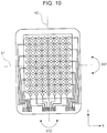
- Fig. 9 is a schematic cross-sectional view illustrating a sample used in the bending-resistance evaluation test.
- Fig. 10 is a schematic plan view illustrating directions of bending in the test.
- Fig. 11 is a graph illustrating an example of the result of the test.
- Fig. 12 is a graph illustrating another example of the result of the test.
- a sample 300 used in the test has a first protective layer 310, a sensor unit 320, a reinforcing sheet 330, and a second protective layer 340.
- the first protective layer 310, the sensor unit 320, the reinforcing sheet 330, and the second protective layer 340 are stacked in this order.
- the sensor unit 320 has a structure in which, for example, a circuit that includes the first transparent electrodes 111 and the second transparent electrodes 121 is formed on a film-like transparent base made of polyethylene terephthalate (PET).
- PET polyethylene terephthalate
- two adjacent first transparent electrodes 111 are electrically connected to each other via the bridge wiring member 20, and two adjacent second transparent electrodes 121 are electrically connected to each other via the coupling member 122.
- the reinforcing sheet 330 is formed of polyethylene terephthalate (PET).
- PET polyethylene terephthalate
- the reinforcing sheet 330 is bonded onto the sensor unit 320 with an optical clear adhesive layer therebetween.
- a protective layer is provided on either surface of a stacked assembly formed of the sensor unit 320 and the reinforcing sheet 330.
- the first protective layer 310 is provided under the sensor unit 320
- the second protective layer 340 is provided over the reinforcing sheet 330.
- the first protective layer 310 and the second protective layer 340 each has a base formed of polyethylene terephthalate (PET) and an optical clear adhesive layer formed of an acrylic adhesive layer.
- PET polyethylene terephthalate
- the first protective layer 310 is bonded to the sensor unit 320 with the optical clear adhesive layer formed of an acrylic adhesive layer.
- the second protective layer 340 is bonded to the reinforcing sheet 330 with the optical clear adhesive layer formed of an acrylic adhesive layer.
- the present inventor used the above-described sample illustrated in Fig. 9 to conduct the bending-resistance evaluation test using a mandrel bending tester.
- the bridge wiring members 20 provided in the sensor unit 320 of a first sample extend in a direction parallel to the first axis A1 illustrated in Fig. 10 .
- the first sample was bent in the direction indicated by the arrow A12 illustrated in Fig. 10 along the second axis A2, which is orthogonal to the first axis A1. Therefore, the direction in which the bridge wiring members 20 extend is orthogonal to the second axis A2 of the direction of bending.
- the bridge wiring members 20 provided in the sensor unit 320 of a second sample extend in the direction parallel to the first axis A1 illustrated in Fig. 10 .
- the second sample was bent in the direction indicated by the arrow A11 illustrated in Fig. 10 along the first axis A1. Therefore, the direction in which the bridge wiring members 20 extend is parallel to the first axis A1 of the direction of bending.
- the first sample was bent once in the direction indicated by the arrow A12 along the second axis A2.
- the second sample was bent once in the direction indicated by the arrow A11 along the first axis A1.
- changes in an electrical inspection value that is, changes from a value before application of the load to a value after application of the load.
- CX is a correction value of the capacitance of the sensor unit 320.
- the bend radius is set to ⁇ 20, ⁇ 16, ⁇ 10, ⁇ 8, ⁇ 6, and ⁇ 4.
- the axes of bending are the second axis A2 and the first axis A1 as described above.
- the acceptable range of the amount of change in the electrical inspection value is "within ⁇ 2". Accordingly, regarding the first sample, in a case where the bend radius is ⁇ 6 or more, the possibility of damage, such as a crack, occurring in the bridge wiring members 20 can be reduced and the possibility of the sensor function of the sensor unit 320 being affected can be reduced.
- the acceptable range of the amount of change in the electrical inspection value is "within ⁇ 2" as in the case of the first sample. Accordingly, regarding the second sample, in a case where the bend radius is ⁇ 4 or more, the possibility of damage, such as a crack, occurring in the bridge wiring members 20 can be reduced and the possibility of the sensor function of the sensor unit 320 being affected can be reduced.
- the bridge wiring members 20 are damaged to a smaller degree in the second sample than in the first sample even if the bend radius of the second sample is decreased. That is, it is found that, in the case where the direction in which the bridge wiring members 20 extend is parallel to the axis of the direction of bending, the bridge wiring members 20 are damaged to a smaller degree than in the case where the direction in which the bridge wiring members 20 extend is orthogonal to the axis of the direction of bending. Based on the above-described result, making the direction in which the bridge wiring members 20 extend close to a direction parallel to the axial direction of the curved surface in the second portion 170 illustrated in Fig. 2(b) is effective in suppressing damage occurring in the bridge wiring members 20.
Abstract
Description
- The present invention relates to a capacitive sensor and relates specifically to a capacitive sensor that has a bridge structure (electrode-crossing structure) and that is bonded to a panel having a curved surface.
- A typical capacitive sensor includes a plurality of transparent electrodes having light transparency. In such a capacitive sensor, which has a bridge structure, a plurality of first transparent electrodes are coupled to each other in a first direction via bridge wires, and a plurality of second transparent electrodes are coupled to each other in a second direction via coupling members. The plurality of bridge wires extend in the same direction throughout substantially the entire area in which the transparent electrodes are provided.
-
PTL 1 discloses an input device that includes a surface panel having a curved surface and a film sensor bonded to the surface panel with an adhesive therebetween. - PTL 1: Japanese Unexamined Patent Application Publication No.
2015-49847 - The film sensor bonded to the surface panel having a curved surface is subjected to bending stress in a portion that is bonded to the curved-surface portion of the surface panel. Then, damage, such as a crack, may occur in a bridge wire, and the resistance of the bridge wire may change accordingly, in which there is room for improvement. When the resistance of the bridge wire changes, the sensor function may be affected.
- To reduce the possibility of damage, such as a crack, occurring in a bridge wire, the direction in which the bridge wires extend can be changed. However, in a case where the plurality of bridge wires extend in the same direction and the capacitive sensor is used for, for example, a display device, the pattern of the bridge wires may be visible from outside the display device depending on the arrangement relationship between the capacitive sensor and the display.
- The present invention has been made to address the above-described existing issues, and an object thereof is to provide a capacitive sensor in which damage in the bridge structure can be suppressed and the possibility of the sensor function becoming defective can be reduced even in a case where the capacitive sensor is bonded to a panel having a curved surface.
- A capacitive sensor according to an aspect of the present invention is a capacitive sensor to be bonded to a panel having a flat-surface portion and a curved-surface portion, including: a plurality of first transparent electrodes arranged side by side in a first direction in a detection area and having light transparency; a plurality of second transparent electrodes arranged side by side in a second direction crossing the first direction in the detection area and having light transparency; a coupling member provided integrally with either the plurality of first transparent electrodes or the plurality of second transparent electrodes to electrically connect the plurality of first transparent electrodes or the plurality of second transparent electrodes, to which the coupling member is provided, to each other; and a bridge wiring member provided separately from the plurality of first transparent electrodes or the plurality of second transparent electrodes, to which the coupling member is not provided, in a portion where the bridge wiring member crosses the coupling member, to electrically connect the plurality of first transparent electrodes or the plurality of second transparent electrodes, to which the bridge wiring member is provided, to each other. A direction in which the coupling member extends in a second portion that is bonded to the curved-surface portion is different from a direction in which the coupling member extends in a first portion that is bonded to the flat-surface portion.
- When a capacitive sensor is bonded to a panel having a curved-surface portion, a portion that is bonded to the curved-surface portion is subjected to bending stress. Then, damage, such as a crack, may occur in a bridge wiring member, and the resistance of the bridge wiring member may change accordingly. When the resistance of the bridge wiring member changes, the sensor function of the capacitive sensor may be affected.
- To address this issue, in the capacitive sensor according to an aspect of the present invention, the direction in which the coupling member extends in the second portion, which is bonded to the curved-surface portion, is different from the direction in which the coupling member extends in the first portion, which is bonded to the flat-surface portion. Therefore, the direction in which the bridge wiring member extends in the second portion can be made different from the direction in which the bridge wiring member extends in the first portion.
- Accordingly, the bending resistance of the capacitive sensor can be increased. That is, even in a case where the capacitive sensor is bonded to the panel having the curved-surface portion, the possibility of damage, such as a crack, occurring in the bridge wiring member can be reduced. As a result, changes in the resistance of the bridge wiring member can be suppressed, and the possibility of the sensor function of the capacitive sensor being affected can be reduced. The bending resistance of the capacitive sensor is increased, and therefore, the capacitive sensor can be bonded to a panel having a curved surface of a smaller radius of curvature.
- In the capacitive sensor according to the present invention, the direction in which the coupling member extends in the second portion may be orthogonal to the direction in which the coupling member extends in the first portion. Accordingly, the direction in which the bridge wiring member extends in the second portion can be made close to a direction orthogonal to the direction in which the bridge wiring member extends in the first portion. As a result, even in the case where the capacitive sensor is bonded to the panel having the curved-surface portion, the possibility of damage, such as a crack, occurring in the bridge wiring member can be further reduced.
- In the capacitive sensor according to the present invention, a direction in which the bridge wiring member extends in the second portion may cross a direction in which the bridge wiring member extends in the first portion. Accordingly, the direction in which the bridge wiring member extends in the second portion can be made to cross the direction of bending stress to which the second portion is subjected. As a result, even in the case where the capacitive sensor is bonded to the panel having the curved-surface portion, the possibility of damage, such as a crack, occurring in the bridge wiring member can be reduced, and the possibility of the sensor function of the capacitive sensor being affected can be reduced accordingly.
- In the capacitive sensor according to the present invention, a direction in which the bridge wiring member extends in the second portion may be orthogonal to a direction in which the bridge wiring member extends in the first portion. Accordingly, the direction in which the bridge wiring member extends in the second portion can be made orthogonal to the direction of bending stress to which the second portion is subjected. As a result, even in the case where the capacitive sensor is bonded to the panel having the curved-surface portion, the possibility of damage, such as a crack, occurring in the bridge wiring member can be reduced with more certainty, and the possibility of the sensor function of the capacitive sensor being affected can be reduced with more certainty accordingly.
- In the capacitive sensor according to the present invention, in the first portion, the coupling member may be provided to the plurality of second transparent electrodes, and the bridge wiring member may be provided to the plurality of first transparent electrodes, and in the second portion, the coupling member may be provided to the plurality of first transparent electrodes, and the bridge wiring member may be provided to the plurality of second transparent electrodes. Accordingly, the possibility of damage, such as a crack, occurring in the bridge wiring member can be reduced without making the arrangement relation of the first transparent electrodes and the second transparent electrodes in the first portion and that in the second portion different from each other.
- In the capacitive sensor according to the present invention, in both the first portion and the second portion, the coupling member may be provided to the plurality of second transparent electrodes, and the bridge wiring member may be provided to the plurality of first transparent electrodes. Accordingly, the connection relation of the plurality of first transparent electrodes being electrically connected to each other via the bridge wiring member and the connection relation of the plurality of second transparent electrodes being electrically connected to each other via the coupling member in the first portion remain the same in the second portion. The direction in which the coupling member extends and the direction in which the bridge wiring member extends in the first portion can be made different from those in the second portion. Therefore, the possibility of damage, such as a crack, occurring in the bridge wiring member can be reduced without making the connection relation of the plurality of first transparent electrodes and the connection relation of the plurality of second transparent electrodes in the first portion and those in the second portion different from each other.
- In the capacitive sensor according to the present invention, the first transparent electrodes may have a rhombus shape, the first transparent electrodes in the second portion may each have an extending portion extending outward from a portion of the rhombus shape, the bridge wiring member in the first portion may be connected to an end portion of the rhombus shape and extend in the first direction, and the bridge wiring member in the second portion may be connected to an end portion of the extending portion and extend in a direction crossing the first direction.
- Accordingly, the connection relation of the plurality of first transparent electrodes being electrically connected to each other via the bridge wiring member and the connection relation of the plurality of second transparent electrodes being electrically connected to each other via the coupling member in the first portion remain the same in the second portion. The direction in which the bridge wiring member extends in the second portion can be made to cross the direction of bending stress to which the second portion is subjected. The bridge wiring member in the first portion is connected to the end portion of the rhombus shape and extends in the first direction. As a result, even in a case where the capacitive sensor is used for, for example, a display device, the possibility of the pattern of the bridge wiring member being visible from outside the display device can be reduced.
- In the capacitive sensor according to the present invention, the first transparent electrodes may have a rhombus shape, the first transparent electrodes in the second portion may each have an extending portion extending outward from a portion of the rhombus shape, the bridge wiring member in the first portion may be connected to an end portion of the rhombus shape and extend in the first direction, and the bridge wiring member in the second portion may be connected to an end portion of the extending portion and extend in a direction orthogonal to the first direction.
- Accordingly, the connection relation of the plurality of first transparent electrodes being electrically connected to each other via the bridge wiring member and the connection relation of the plurality of second transparent electrodes being electrically connected to each other via the coupling member in the first portion remain the same in the second portion. The direction in which the bridge wiring member extends in the second portion can be made orthogonal to the direction of bending stress to which the second portion is subjected. The bridge wiring member in the first portion is connected to the end portion of the rhombus shape and extends in the first direction. As a result, even in the case where the capacitive sensor is used for, for example, a display device, the possibility of the pattern of the bridge wiring member being visible from outside the display device can be reduced with more certainty.
- According to the present invention, it is possible to provide a capacitive sensor in which damage in the bridge structure can be suppressed and the possibility of the sensor function becoming defective can be reduced even in a case where the capacitive sensor is bonded to a panel having a curved surface.
-
- [
Fig. 1] Fig. 1 is a schematic plan view illustrating a capacitive sensor according to the present embodiment. - [
Fig. 2] Fig. 2 includes schematic plan views for describing a process in which the capacitive sensor according to the present embodiment is bonded to a panel. - [
Fig. 3] Fig. 3 is a schematic enlarged view illustrating a bridge wiring member in a first portion that is bonded to a flat-surface portion of a panel. - [
Fig. 4] Fig. 4 is a schematic cross-sectional view taken along line S1-S1 illustrated inFig. 3 . - [
Fig. 5] Fig. 5 is a schematic enlarged view illustrating a bridge wiring member in a second portion that is bonded to a curved-surface portion of a panel. - [
Fig. 6] Fig. 6 is a schematic cross-sectional view taken along line S2-S2 illustrated inFig. 5 . - [
Fig. 7] Fig. 7 is a schematic enlarged view illustrating another bridge structure in the first portion. - [
Fig. 8] Fig. 8 is a schematic enlarged view illustrating another bridge structure in the second portion. - [
Fig. 9] Fig. 9 is a schematic cross-sectional view illustrating a sample used in a bending-resistance evaluation test. - [
Fig. 10] Fig. 10 is a schematic plan view illustrating directions of bending in the test. - [
Fig. 11] Fig. 11 is a graph illustrating an example of the result of the test. - [
Fig. 12] Fig. 12 is a graph illustrating another example of the result of the test. - Hereinafter, an embodiment of the present invention will be described with reference to the drawings. Note that, in the drawings, similar constituent elements are assigned the same reference numerals, and detailed descriptions thereof will be omitted as appropriate.
-
Fig. 1 is a schematic plan view illustrating a capacitive sensor according to the present embodiment.Fig. 2 includes schematic plan views for describing a process in which the capacitive sensor according to the present embodiment is bonded to a panel.Fig. 3 is a schematic enlarged view illustrating a bridge wiring member in a first portion that is bonded to a flat-surface portion of a panel. -
Fig. 4 is a schematic cross-sectional view taken along line S1-S1 illustrated inFig. 3 .Fig. 5 is a schematic enlarged view illustrating a bridge wiring member in a second portion that is bonded to a curved-surface portion of a panel.Fig. 6 is a schematic cross-sectional view taken along line S2-S2 illustrated inFig. 5 . -
Fig. 2(a) is a schematic plan view illustrating a state before the capacitive sensor according to the present embodiment is bonded to a panel.Fig. 2(b) is a schematic plan view illustrating a state after the capacitive sensor according to the present embodiment has been bonded to the panel. - The terms "transparent" and "light transparency" used herein indicate a state where the visible-light transmittance is 50% or more (preferably, 80% or more). Further, it is preferable that the haze value be 6% or less.
- As illustrated in
Fig. 2(a) and Fig. 2(b) , acapacitive sensor 1 according to the present embodiment is bonded to a surface on one side of apanel 200 with an adhesive (not illustrated) therebetween. Thepanel 200 has a flat-surface portion 210 formed so as to have a flat surface and a curved-surface portion 220 formed so as to have a curved surface. In thepanel 200 illustrated inFig. 2(a) and Fig. 2(b) , the curved-surface portion 220 is provided on either side of the flat-surface portion 210. The examples of the material of thepanel 200 include a glass base and a plastic base having light transparency. - The
capacitive sensor 1 has flexibility. As illustrated inFig. 2(b) , thecapacitive sensor 1 is curved along the curved surface of thepanel 200 and bonded to the surface on one side of thepanel 200. Accordingly, thecapacitive sensor 1 has afirst portion 160, which is bonded to the flat-surface portion 210 of thepanel 200, and asecond portion 170, which is bonded to the curved-surface portion 220 of thepanel 200. - As illustrated in
Fig. 1 andFig. 3 toFig. 6 , thecapacitive sensor 1 according to the present embodiment includes asubstrate 10,first electrodes 11,second electrodes 12,bridge wiring members 20, an optical clear adhesive (OCA)layer 35, and aprotective layer 50. - The
substrate 10 has light transparency and is formed of, for example, a film-like transparent base made of polyethylene terephthalate (PET) or a glass base. - The
first electrodes 11 and thesecond electrodes 12 are provided in a detection area S (an area in which operations using an operation device, such as a finger, can be performed) of thesubstrate 10. Eachfirst electrode 11 extends in an X direction (first direction) along asurface 10a of thesubstrate 10. Eachsecond electrode 12 extends in a Y direction (second direction) orthogonal to the X direction along thesurface 10a of thesubstrate 10. Thefirst electrodes 11 are isolated from thesecond electrodes 12. In the present embodiment, the plurality offirst electrodes 11 are arranged in the Y direction at predetermined intervals, and the plurality ofsecond electrodes 12 are arranged in the X direction at predetermined intervals. - As illustrated in
Fig. 3 andFig. 5 , eachfirst electrode 11 has a plurality of firsttransparent electrodes 111. In the present embodiment, the plurality of firsttransparent electrodes 111 have a shape close to a rhombus shape and are arranged side by side in the X direction. That is, the plurality of firsttransparent electrodes 111 are arranged side by side in the X direction. Eachsecond electrode 12 has a plurality of secondtransparent electrodes 121. The plurality of secondtransparent electrodes 121 have a shape close to a rhombus shape and are arranged side by side in the Y direction. That is, the plurality of secondtransparent electrodes 121 are arranged side by side in the Y direction, which crosses the X direction. - The first
transparent electrodes 111 and the secondtransparent electrodes 121 are formed of a transparent conductive material, such as ITO (Indium Tin Oxide), SnO2, or ZnO, by, for example, sputtering or vapor deposition. Examples of the transparent conductive material include a metal nanowire, typically, a silver nanowire, a thin metal sheet formed into a mesh shape, and a conductive polymer in addition to ITO, SnO2, and ZnO. The firsttransparent electrodes 111 and the secondtransparent electrodes 121 may be formed by screen printing using a conductive ink. - Alternatively, the first
transparent electrodes 111 and the secondtransparent electrodes 121 may be formed by using a photoconductive sheet (a sheet formed of a dry film resist having a conductive layer). When such a photoconductive sheet is used, the firsttransparent electrodes 111 and the secondtransparent electrodes 121 can be formed in a highly productive manner by bonding this sheet and performing exposure and development. - To each of the plurality of
first electrodes 11, alead wire 11a, which externally extends from the detection area S, is connected, as illustrated inFig. 1 . To each of the plurality ofsecond electrodes 12, alead wire 12a, which externally extends from the detection area S, is connected. To eachfirst electrode 11, a drive voltage is applied via thelead wire 11a. To eachsecond electrode 12, a drive voltage is applied via thelead wire 12a. Thelead wires 11a and thelead wires 12a may be formed of a transparent conductive material similar to that used for the firsttransparent electrodes 111 and the secondtransparent electrodes 121 by, for example, sputtering or vapor deposition. Thelead wires 11a and thelead wires 12a need not have light transparency, and therefore, may be formed of another metallic material. - As illustrated in
Fig. 3 to Fig. 6 , thefirst electrode 11 and thesecond electrode 12 cross each other at a position where two adjacent firsttransparent electrodes 111 are coupled to each other and at a position where two adjacent secondtransparent electrodes 121 are coupled to each other. In this portion of crossing, thebridge wiring member 20 is provided so that thefirst electrode 11 and thesecond electrode 12 do not come into contact with each other in the portion of crossing. That is, thecapacitive sensor 1 according to the present embodiment has a bridge structure (electrode-crossing structure). - In the
first portion 160 of thecapacitive sensor 1 according to the present embodiment, acoupling member 122 is provided between two adjacent secondtransparent electrodes 121, as illustrated inFig. 3 andFig. 4 . Thecoupling member 122 is provided integrally with the secondtransparent electrodes 121. Therefore, thesecond electrode 12 is formed such that the secondtransparent electrode 121 and thecoupling member 122 are alternately and repeatedly disposed in the Y direction. Thecoupling member 122 electrically connects the secondtransparent electrodes 121 to each other. - Meanwhile, in the
first portion 160 of thecapacitive sensor 1 according to the present embodiment, thebridge wiring member 20 is provided between two adjacent firsttransparent electrodes 111. Thebridge wiring member 20 is provided separately from the firsttransparent electrodes 111 in a portion where thebridge wiring member 20 crosses thecoupling member 122. Therefore, thefirst electrode 11 is formed such that the firsttransparent electrode 111 and thebridge wiring member 20 are alternately and repeatedly disposed in the X direction. Thebridge wiring member 20 illustrated inFig. 3 extends in the X direction. However, in thecapacitive sensor 1 according to the present embodiment, the direction in which the coupling members extend and the direction in which thebridge wiring members 20 extend do not remain the same throughout the detection area S. The pattern of the coupling members and thebridge wiring members 20 in thesecond portion 170 of thecapacitive sensor 1 according to the present embodiment will be described in detail below. - On the surface of the
coupling member 122, an insulatinglayer 30 is formed. As illustrated inFig. 4 , the space between thecoupling member 122 and each firsttransparent electrode 111 is filled with the insulatinglayer 30, and the insulatinglayer 30 runs onto the surfaces of the firsttransparent electrodes 111 to some extent. As the insulatinglayer 30, for example, a novolac resin (resist) is used. - As illustrated in
Fig. 4 , thebridge wiring member 20 is formed so as to extend from asurface 30a of the insulatinglayer 30 to the surfaces of the respective firsttransparent electrodes 111 located on the respective sides of the insulatinglayer 30. Thebridge wiring member 20 electrically connects the firsttransparent electrodes 111 to each other. - As illustrated in
Fig. 4 , the insulatinglayer 30 is provided on the surface of thecoupling member 122, which connects the secondtransparent electrodes 121 to each other, and thebridge wiring member 20, which connects the firsttransparent electrodes 111 to each other, is provided on the surface of the insulatinglayer 30. As described above, the insulatinglayer 30 is interposed between thecoupling member 122 and thebridge wiring member 20 to create a state where the firsttransparent electrodes 111 are electrically insulated from the secondtransparent electrodes 121. In the present embodiment, the firsttransparent electrodes 111 and the secondtransparent electrodes 121 can be formed on the same surface (thesurface 10a of the substrate 10) to make thecapacitive sensor 1 thinner. - All the
coupling members 122, the insulatinglayer 30, and thebridge wiring members 20 are located within the detection area S and have light transparency similarly to the firsttransparent electrodes 111 and the secondtransparent electrodes 121. - The
protective layer 50 is provided above thebridge wiring members 20 with the opticalclear adhesive layer 35 therebetween. Theprotective layer 50 is bonded to thesubstrate 10 with the opticalclear adhesive layer 35 therebetween. The material of theprotective layer 50 is not limited to a specific material. As the material of theprotective layer 50, a glass base or a plastic base is preferably used. The opticalclear adhesive layer 35 is, for example, an acrylic adhesive or a two-sided adhesive tape. - In the
capacitive sensor 1 illustrated inFig. 1 , when a finger F comes into contact with anoperation surface 50a of theprotective layer 50, as illustrated inFig. 4 , a capacitance is formed between the finger F and the firsttransparent electrode 111 that is close to the finger F and between the finger F and the secondtransparent electrode 121 that is close to the finger F. On the basis of changes in the capacitances at this time, thecapacitive sensor 1 can calculate the position at which the finger F comes into contact. Thecapacitive sensor 1 determines the Y coordinate of the position of the finger F on the basis of a change in the capacitance between the finger F and thefirst electrode 11 and determines the X coordinate of the position of the finger F on the basis of a change in the capacitance between the finger F and the second electrode 12 (self-capacitance detection type). - Alternatively, the
capacitive sensor 1 may be of a mutual-capacitance detection type. That is, thecapacitive sensor 1 may apply a drive voltage to one electrode among onefirst electrode 11 and onesecond electrode 12 and sense a change in the capacitance between the finger F and the other electrode among thefirst electrode 11 and thesecond electrode 12. Accordingly, thecapacitive sensor 1 determines the Y coordinate of the position of the finger F from the other electrode and determines the X coordinate of the position of the finger F from the one electrode. - When the
capacitive sensor 1 is bonded to thepanel 200, thesecond portion 170 of thecapacitive sensor 1 is subjected to bending stress. Then, damage, such as a crack, may occur in a bridge wiring member, and the resistance of the bridge wiring member may change accordingly. When the resistance of the bridge wiring member changes, the sensor function of the capacitive sensor may be affected. - To address this issue, in the
second portion 170 of thecapacitive sensor 1 according to the present embodiment, acoupling member 112 is provided between two adjacent firsttransparent electrodes 111, as illustrated inFig. 5 andFig. 6 . Thecoupling member 112 is provided integrally with the firsttransparent electrodes 111. Therefore, thefirst electrode 11 is formed such that the firsttransparent electrode 111 and thecoupling member 112 are alternately and repeatedly disposed in the X direction. Thecoupling member 112 electrically connects the firsttransparent electrodes 111 to each other. - Meanwhile, in the
second portion 170 of thecapacitive sensor 1 according to the present embodiment, thebridge wiring member 20 is provided between two adjacent secondtransparent electrodes 121. Thebridge wiring member 20 is provided separately from the secondtransparent electrodes 121 in a portion where thebridge wiring member 20 crosses thecoupling member 112. Therefore, thesecond electrode 12 is formed such that the secondtransparent electrode 121 and thebridge wiring member 20 are alternately and repeatedly disposed in the Y direction. Thebridge wiring member 20 illustrated inFig. 5 extends in the Y direction. - On the surface of the
coupling member 112, the insulatinglayer 30 is formed. As illustrated inFig. 6 , the space between thecoupling member 112 and each secondtransparent electrode 121 is filled with the insulatinglayer 30, and the insulatinglayer 30 runs onto the surfaces of the secondtransparent electrodes 121 to some extent. As the insulatinglayer 30, for example, a novolac resin (resist) is used. - As illustrated in
Fig. 6 , thebridge wiring member 20 is formed so as to extend from thesurface 30a of the insulatinglayer 30 to the surfaces of the respective secondtransparent electrodes 121 located on the respective sides of the insulatinglayer 30. Thebridge wiring member 20 electrically connects the secondtransparent electrodes 121 to each other. The structure of the remaining portion in thesecond portion 170 is the same as that in thefirst portion 160. - As described above, in the
first portion 160 of thecapacitive sensor 1, thecoupling members 122 are provided integrally with the plurality of secondtransparent electrodes 121 to electrically connect the plurality of secondtransparent electrodes 121 to each other. Thebridge wiring members 20 are provided separately from the plurality of firsttransparent electrodes 111 in respective portions, in each of which thebridge wiring member 20 crosses thecoupling member 122, to electrically connect the plurality of firsttransparent electrodes 111 to each other. - Meanwhile, in the
second portion 170 of thecapacitive sensor 1, thecoupling members 112 are provided integrally with the plurality of firsttransparent electrodes 111 to electrically connect the plurality of firsttransparent electrodes 111 to each other. Thebridge wiring members 20 are provided separately from the plurality of secondtransparent electrodes 121 in respective portions, in each of which thebridge wiring member 20 crosses thecoupling member 112, to electrically connect the plurality of secondtransparent electrodes 121 to each other. - Therefore, in the
capacitive sensor 1 according to the present embodiment, the direction in which thecoupling members 112 extend in thesecond portion 170 is different from the direction in which thecoupling members 122 extend in thefirst portion 160. Specifically, the directions are orthogonal to each other. - Accordingly, the direction in which the
bridge wiring members 20 extend in thesecond portion 170 is different from the direction in which thebridge wiring members 20 extend in thefirst portion 160. That is, the direction in which thebridge wiring members 20 extend in thesecond portion 170 crosses the direction in which thebridge wiring members 20 extend in thefirst portion 160. Specifically, the directions are orthogonal to each other. Therefore, as illustrated inFig. 5 , the direction in which thebridge wiring member 20 extends in thesecond portion 170 is orthogonal to the direction of bending stress to which thesecond portion 170 is subjected (in the present embodiment, the X direction). - The term "direction of bending stress" used herein indicates a direction parallel to the direction of tensile stress and compressive stress to which the capacitive sensor is subjected due to a bending moment produced in the capacitive sensor.
- In the
capacitive sensor 1 according to the present embodiment, the direction in which thebridge wiring members 20 extend in thesecond portion 170, which is bonded to the curved-surface portion 220 of thepanel 200, is orthogonal to the direction of bending stress to which thesecond portion 170 is subjected, and therefore, the bending resistance of thecapacitive sensor 1 can be increased. As a result, even in a case where thecapacitive sensor 1 is bonded to thepanel 200 having a curved surface, the possibility of damage, such as a crack, occurring in thebridge wiring members 20 can be reduced. Accordingly, changes in the resistances of thebridge wiring members 20 can be suppressed, and the possibility of the sensor function of thecapacitive sensor 1 being affected can be reduced. - The bending resistance of the
capacitive sensor 1 is increased, and therefore, thecapacitive sensor 1 can be bonded to thepanel 200 having a curved surface of a smaller radius of curvature. - It is more preferable that the angle between the direction in which the
bridge wiring members 20 extend in thesecond portion 170 and the direction of bending stress to which thesecond portion 170 is subjected be about 90°± 30° . - Now, other bridge structures are described with reference to the drawings.
-
Fig. 7 is a schematic enlarged view illustrating another bridge structure in the first portion.Fig. 8 is a schematic enlarged view illustrating another bridge structure in the second portion. - As illustrated in
Fig. 7 , in thefirst portion 160 of thecapacitive sensor 1, the firsttransparent electrodes 111 have a rhombus shape. The secondtransparent electrodes 121 have a rhombus shape, and one of the adjacent secondtransparent electrodes 121 is connected to the other secondtransparent electrode 121 via thecoupling member 122. Thebridge wiring member 20 is connected to end portions of the rhombus shapes of the firsttransparent electrodes 111 and extends in the X direction. - Meanwhile, as illustrated in
Fig. 8 , in thesecond portion 170 of thecapacitive sensor 1, the firsttransparent electrodes 111 have a substantially rhombus shape and each have an extendingportion 115, which extends outward from the rhombus portion. The extendingportion 115 extends in a direction at about 45° relative to the X direction (that is, the direction of bending stress). Thebridge wiring member 20 is connected to end portions of the extendingportions 115 of the firsttransparent electrodes 111 and extends in the Y direction. - As described above, in the bridge structures illustrated in
Fig. 7 andFig. 8 , the direction (Y direction) in which thebridge wiring member 20 extends in thesecond portion 170 crosses the direction (X direction) in which thebridge wiring member 20 extends in thefirst portion 160. Specifically, the directions are orthogonal to each other. - In the
second portion 170 of thecapacitive sensor 1, the secondtransparent electrodes 121 have a substantially rhombus shape and each have an extendingportion 125, which extends outward from the rhombus portion. The extendingportion 125 is connected to thecoupling member 122. That is, in this specific example, two adjacent secondtransparent electrodes 121 are connected to each other via the respective extendingportions 125 and thecoupling member 122. Thecoupling member 122 extends through the space between the extendingportions 115 of the respective firsttransparent electrodes 111. - In the above-described structures, the connection relation of the plurality of first
transparent electrodes 111 being electrically connected to each other via thebridge wiring members 20 and the connection relation of the plurality of secondtransparent electrodes 121 being electrically connected to each other via thecoupling members 122 in thefirst portion 160 remain the same in thesecond portion 170. The direction in which thecoupling members 122 extend and the direction in which thebridge wiring members 20 extend in thefirst portion 160 can be made different from those in thesecond portion 170. Therefore, the possibility of damage, such as a crack, occurring in thebridge wiring members 20 can be reduced and the possibility of the sensor function of thecapacitive sensor 1 being affected can be reduced without making the connection relation of the plurality of firsttransparent electrodes 111 and the connection relation of the plurality of secondtransparent electrodes 121 in thefirst portion 160 and those in thesecond portion 170 different from each other. Further, the direction in which thebridge wiring members 20 extend in thefirst portion 160 is made different from the direction in which thebridge wiring members 20 extend in thesecond portion 170. Therefore, even in a case where thecapacitive sensor 1 is used for, for example, a display device, the possibility of the pattern of thebridge wiring members 20 being visible from outside the display device can be reduced. - Now, an example of a bending-resistance evaluation test conducted by the present inventor is described with reference to the drawings.
-
Fig. 9 is a schematic cross-sectional view illustrating a sample used in the bending-resistance evaluation test.Fig. 10 is a schematic plan view illustrating directions of bending in the test.Fig. 11 is a graph illustrating an example of the result of the test.Fig. 12 is a graph illustrating another example of the result of the test. - The present inventor conducted the bending-resistance evaluation test using the sample illustrated in
Fig. 9 and a mandrel bending tester. As illustrated inFig. 9 , asample 300 used in the test has a firstprotective layer 310, asensor unit 320, a reinforcingsheet 330, and a secondprotective layer 340. The firstprotective layer 310, thesensor unit 320, the reinforcingsheet 330, and the secondprotective layer 340 are stacked in this order. - The
sensor unit 320 has a structure in which, for example, a circuit that includes the firsttransparent electrodes 111 and the secondtransparent electrodes 121 is formed on a film-like transparent base made of polyethylene terephthalate (PET). In thesample 300, two adjacent firsttransparent electrodes 111 are electrically connected to each other via thebridge wiring member 20, and two adjacent secondtransparent electrodes 121 are electrically connected to each other via thecoupling member 122. - The reinforcing
sheet 330 is formed of polyethylene terephthalate (PET). The reinforcingsheet 330 is bonded onto thesensor unit 320 with an optical clear adhesive layer therebetween. - On either surface of a stacked assembly formed of the
sensor unit 320 and the reinforcingsheet 330, a protective layer is provided. Specifically, the firstprotective layer 310 is provided under thesensor unit 320, and the secondprotective layer 340 is provided over the reinforcingsheet 330. The firstprotective layer 310 and the secondprotective layer 340 each has a base formed of polyethylene terephthalate (PET) and an optical clear adhesive layer formed of an acrylic adhesive layer. The firstprotective layer 310 is bonded to thesensor unit 320 with the optical clear adhesive layer formed of an acrylic adhesive layer. The secondprotective layer 340 is bonded to the reinforcingsheet 330 with the optical clear adhesive layer formed of an acrylic adhesive layer. - The present inventor used the above-described sample illustrated in
Fig. 9 to conduct the bending-resistance evaluation test using a mandrel bending tester. - The
bridge wiring members 20 provided in thesensor unit 320 of a first sample extend in a direction parallel to the first axis A1 illustrated inFig. 10 . The first sample was bent in the direction indicated by the arrow A12 illustrated inFig. 10 along the second axis A2, which is orthogonal to the first axis A1. Therefore, the direction in which thebridge wiring members 20 extend is orthogonal to the second axis A2 of the direction of bending. - Also, the
bridge wiring members 20 provided in thesensor unit 320 of a second sample extend in the direction parallel to the first axis A1 illustrated inFig. 10 . The second sample was bent in the direction indicated by the arrow A11 illustrated inFig. 10 along the first axis A1. Therefore, the direction in which thebridge wiring members 20 extend is parallel to the first axis A1 of the direction of bending. - The first sample was bent once in the direction indicated by the arrow A12 along the second axis A2. The second sample was bent once in the direction indicated by the arrow A11 along the first axis A1. Then, changes in an electrical inspection value (CX), that is, changes from a value before application of the load to a value after application of the load, are checked. Note that "CX" is a correction value of the capacitance of the
sensor unit 320. The bend radius is set to φ20, φ16, φ10, φ8, φ6, and φ4. The axes of bending are the second axis A2 and the first axis A1 as described above. - An example of the result of testing the first sample is illustrated in
Fig. 11 . Based on the present inventor's experiences, the acceptable range of the amount of change in the electrical inspection value, that is, changes from a value before the test to a value after the test, is "within ±2". Accordingly, regarding the first sample, in a case where the bend radius is φ6 or more, the possibility of damage, such as a crack, occurring in thebridge wiring members 20 can be reduced and the possibility of the sensor function of thesensor unit 320 being affected can be reduced. - An example of the result of testing the second sample is illustrated in
Fig. 12 . The acceptable range of the amount of change in the electrical inspection value, that is, changes from a value before the test to a value after the test, is "within ±2" as in the case of the first sample. Accordingly, regarding the second sample, in a case where the bend radius is φ4 or more, the possibility of damage, such as a crack, occurring in thebridge wiring members 20 can be reduced and the possibility of the sensor function of thesensor unit 320 being affected can be reduced. - Based on the result of the bending-resistance evaluation test conducted for the first sample and for the second sample, it is found that the
bridge wiring members 20 are damaged to a smaller degree in the second sample than in the first sample even if the bend radius of the second sample is decreased. That is, it is found that, in the case where the direction in which thebridge wiring members 20 extend is parallel to the axis of the direction of bending, thebridge wiring members 20 are damaged to a smaller degree than in the case where the direction in which thebridge wiring members 20 extend is orthogonal to the axis of the direction of bending. Based on the above-described result, making the direction in which thebridge wiring members 20 extend close to a direction parallel to the axial direction of the curved surface in thesecond portion 170 illustrated inFig. 2(b) is effective in suppressing damage occurring in thebridge wiring members 20. - The present embodiment and example applications thereof have been described above; however, the present invention is not limited to the examples. For example, an embodiment obtained by a person skilled in the art adding, deleting, or making a design change to any constituent element in the above-described embodiment or example applications thereof as appropriate and an embodiment obtained by a person skilled in the art combining features of the embodiment as appropriate are within the scope of the present invention as long as such embodiments have the spirit of the present invention.
-
- 1
- capacitive sensor
- 10
- substrate
- 10a
- surface
- 11
- first electrode
- 11a
- lead wire
- 12
- second electrode
- 12a
- lead wire
- 20
- bridge wiring member
- 30
- insulating layer
- 30a
- surface
- 35
- optical clear adhesive layer
- 50
- protective layer
- 50a
- operation surface
- 111
- first transparent electrode
- 112
- coupling member
- 115
- extending portion
- 121
- second transparent electrode
- 122
- coupling member
- 125
- extending portion
- 160
- first portion
- 170
- second portion
- 200
- panel
- 210
- flat-surface portion
- 220
- curved-surface portion
- 300
- sample
- 310
- first protective layer
- 320
- sensor unit
- 330
- reinforcing sheet
- 340
- second protective layer
- A1
- first axis
- A11
- arrow
- A12
- arrow
- A2
- second axis
- F
- finger
- S
- detection area
Claims (8)
- A capacitive sensor to be bonded to a panel having a flat-surface portion and a curved-surface portion, comprising:a plurality of first transparent electrodes arranged side by side in a first direction in a detection area and having light transparency;a plurality of second transparent electrodes arranged side by side in a second direction crossing the first direction in the detection area and having light transparency;a coupling member provided integrally with either the plurality of first transparent electrodes or the plurality of second transparent electrodes to electrically connect the plurality of first transparent electrodes or the plurality of second transparent electrodes, to which the coupling member is provided, to each other; anda bridge wiring member provided separately from the plurality of first transparent electrodes or the plurality of second transparent electrodes, to which the coupling member is not provided, in a portion where the bridge wiring member crosses the coupling member, to electrically connect the plurality of first transparent electrodes or the plurality of second transparent electrodes, to which the bridge wiring member is provided, to each other, whereina direction in which the coupling member extends in a second portion that is bonded to the curved-surface portion is different from a direction in which the coupling member extends in a first portion that is bonded to the flat-surface portion.
- The capacitive sensor according to Claim 1, wherein the direction in which the coupling member extends in the second portion is orthogonal to the direction in which the coupling member extends in the first portion.
- The capacitive sensor according to Claim 1 or 2, wherein a direction in which the bridge wiring member extends in the second portion crosses a direction in which the bridge wiring member extends in the first portion.
- The capacitive sensor according to Claim 1 or 2, wherein a direction in which the bridge wiring member extends in the second portion is orthogonal to a direction in which the bridge wiring member extends in the first portion.
- The capacitive sensor according to any one of Claims 1 to 4, wherein
in the first portion, the coupling member is provided to the plurality of second transparent electrodes, and the bridge wiring member is provided to the plurality of first transparent electrodes, and
in the second portion, the coupling member is provided to the plurality of first transparent electrodes, and the bridge wiring member is provided to the plurality of second transparent electrodes. - The capacitive sensor according to any one of Claims 1 to 4, wherein
in both the first portion and the second portion, the coupling member is provided to the plurality of second transparent electrodes, and the bridge wiring member is provided to the plurality of first transparent electrodes. - The capacitive sensor according to Claim 6, wherein
the first transparent electrodes have a rhombus shape,
the first transparent electrodes in the second portion each have an extending portion extending outward from a portion of the rhombus shape,
the bridge wiring member in the first portion is connected to an end portion of the rhombus shape and extends in the first direction, and
the bridge wiring member in the second portion is connected to an end portion of the extending portion and extends in a direction crossing the first direction. - The capacitive sensor according to Claim 6, wherein
the first transparent electrodes have a rhombus shape,
the first transparent electrodes in the second portion each have an extending portion extending outward from a portion of the rhombus shape,
the bridge wiring member in the first portion is connected to an end portion of the rhombus shape and extends in the first direction, and
the bridge wiring member in the second portion is connected to an end portion of the extending portion and extends in a direction orthogonal to the first direction.
Applications Claiming Priority (2)
| Application Number | Priority Date | Filing Date | Title |
|---|---|---|---|
| JP2015242042 | 2015-12-11 | ||
| PCT/JP2016/086534 WO2017099173A1 (en) | 2015-12-11 | 2016-12-08 | Capacitive sensor |
Publications (2)
| Publication Number | Publication Date |
|---|---|
| EP3388927A1 true EP3388927A1 (en) | 2018-10-17 |
| EP3388927A4 EP3388927A4 (en) | 2019-08-07 |
Family
ID=59014224
Family Applications (1)
| Application Number | Title | Priority Date | Filing Date |
|---|---|---|---|
| EP16873066.1A Withdrawn EP3388927A4 (en) | 2015-12-11 | 2016-12-08 | Capacitive sensor |
Country Status (6)
| Country | Link |
|---|---|
| US (1) | US10558308B2 (en) |
| EP (1) | EP3388927A4 (en) |
| JP (1) | JP6509370B2 (en) |
| KR (1) | KR102039009B1 (en) |
| CN (1) | CN108351734B (en) |
| WO (1) | WO2017099173A1 (en) |
Families Citing this family (2)
| Publication number | Priority date | Publication date | Assignee | Title |
|---|---|---|---|---|
| KR102430807B1 (en) * | 2017-12-12 | 2022-08-09 | 엘지디스플레이 주식회사 | Flexible Touch Screen Panel And Method For Manufacturing The Same |
| US11640210B2 (en) * | 2020-11-27 | 2023-05-02 | Tpk Advanced Solutions Inc. | Touch panel and touch device |
Family Cites Families (25)
| Publication number | Priority date | Publication date | Assignee | Title |
|---|---|---|---|---|
| JP2007272644A (en) * | 2006-03-31 | 2007-10-18 | Gunze Ltd | Transparent touch panel |
| WO2010029979A1 (en) * | 2008-09-12 | 2010-03-18 | オプトレックス株式会社 | Electrostatic capacity type touch panel, display device, and electrostatic capacity type touch panel manufacturing method |
| US8593410B2 (en) * | 2009-04-10 | 2013-11-26 | Apple Inc. | Touch sensor panel design |
| KR101100987B1 (en) * | 2010-03-23 | 2011-12-30 | 삼성모바일디스플레이주식회사 | Touch Screen Panel |
| KR101706234B1 (en) * | 2010-10-13 | 2017-02-15 | 엘지디스플레이 주식회사 | Touch panel and display device associated with the same |
| US8717330B2 (en) * | 2010-11-22 | 2014-05-06 | Industrial Technology Research Institute | Flexible projective capacitive touch sensor structure |
| CN102253776B (en) * | 2011-07-06 | 2013-07-03 | 汕头超声显示器有限公司 | Electrode bridging connection structure for inhibiting picture interference of capacitance type touch screen |
| KR101375335B1 (en) * | 2012-05-15 | 2014-03-18 | 삼성디스플레이 주식회사 | Display Device and Control method thereof |
| TWI460772B (en) * | 2012-06-29 | 2014-11-11 | Innocom Tech Shenzhen Co Ltd | Touch panel and touch display device |
| US9419065B2 (en) * | 2012-08-07 | 2016-08-16 | Apple Inc. | Flexible displays |
| TWI599921B (en) * | 2012-09-07 | 2017-09-21 | 財團法人工業技術研究院 | Touch panel |
| KR102077316B1 (en) * | 2012-11-14 | 2020-04-08 | 삼성디스플레이 주식회사 | flexible touch screen panel and flexible display device with the same |
| TWI494839B (en) * | 2013-01-18 | 2015-08-01 | Elan Microelectronics Corp | Touch sensing structure |
| KR102075040B1 (en) * | 2013-02-05 | 2020-02-11 | 삼성디스플레이 주식회사 | Touch Screen Panel |
| US10120447B2 (en) * | 2013-06-24 | 2018-11-06 | Northwestern University | Haptic display with simultaneous sensing and actuation |
| JP6176716B2 (en) | 2013-09-04 | 2017-08-09 | アルプス電気株式会社 | Input device and portable device using the same |
| KR102119603B1 (en) * | 2013-09-06 | 2020-06-08 | 엘지이노텍 주식회사 | Touch window and display with the same |
| CN104423715B (en) * | 2013-09-11 | 2019-07-23 | Lg伊诺特有限公司 | Touch window and the display including the touch window |
| KR102347532B1 (en) * | 2014-01-23 | 2022-01-05 | 삼성디스플레이 주식회사 | Flexible display apparatus and method of manufacturing thereof |
| CN104881161B (en) * | 2014-02-27 | 2017-12-01 | 财团法人工业技术研究院 | Touch panel |
| US9965113B2 (en) * | 2014-04-14 | 2018-05-08 | Lg Innotek Co., Ltd. | Touch window |
| US10372163B2 (en) * | 2014-05-30 | 2019-08-06 | Semiconductor Energy Laboratory Co., Ltd. | Input device comprising sensor panel, information processing device comprising input device |
| CN105183203A (en) * | 2014-06-13 | 2015-12-23 | 宝宸(厦门)光学科技有限公司 | Touch control panel and touch control type electronic device |
| KR102267357B1 (en) * | 2014-12-15 | 2021-06-21 | 삼성디스플레이 주식회사 | Touch sensor device |
| KR102312260B1 (en) * | 2015-01-09 | 2021-10-13 | 삼성디스플레이 주식회사 | Flexible touch panel and flexible display device |
-
2016
- 2016-12-08 KR KR1020187015825A patent/KR102039009B1/en active IP Right Grant
- 2016-12-08 CN CN201680065446.XA patent/CN108351734B/en not_active Expired - Fee Related
- 2016-12-08 EP EP16873066.1A patent/EP3388927A4/en not_active Withdrawn
- 2016-12-08 WO PCT/JP2016/086534 patent/WO2017099173A1/en unknown
- 2016-12-08 JP JP2017555130A patent/JP6509370B2/en not_active Expired - Fee Related
-
2018
- 2018-03-29 US US15/940,651 patent/US10558308B2/en not_active Expired - Fee Related
Also Published As
| Publication number | Publication date |
|---|---|
| US10558308B2 (en) | 2020-02-11 |
| JP6509370B2 (en) | 2019-05-08 |
| US20180217703A1 (en) | 2018-08-02 |
| JPWO2017099173A1 (en) | 2018-08-09 |
| CN108351734B (en) | 2020-12-01 |
| KR102039009B1 (en) | 2019-10-31 |
| KR20180078315A (en) | 2018-07-09 |
| EP3388927A4 (en) | 2019-08-07 |
| CN108351734A (en) | 2018-07-31 |
| WO2017099173A1 (en) | 2017-06-15 |
Similar Documents
| Publication | Publication Date | Title |
|---|---|---|
| KR102267357B1 (en) | Touch sensor device | |
| US10564784B2 (en) | Capacitive sensor having bending portion and flat portion | |
| CN106775145B (en) | Touch sensor | |
| US8659558B2 (en) | Touch sensing display panel | |
| US8698025B2 (en) | Input device | |
| TWI489356B (en) | Touch display device and touch sensing device | |
| US20160170549A1 (en) | Touch sensor device and display device including the same | |
| US10746770B2 (en) | Capacitive sensor suppressing breakage of electrode linking parts due to electrostatic discharge | |
| JP6735850B2 (en) | Capacitive sensor and equipment | |
| US10558308B2 (en) | Capacitive sensor for panel having flat-surface portion and curved-surface portion | |
| CN212484325U (en) | Input device | |
| KR102146460B1 (en) | Touch sensor and display device comprising the same | |
| JP3173905U (en) | Capacitive touch sensor device |
Legal Events
| Date | Code | Title | Description |
|---|---|---|---|
| STAA | Information on the status of an ep patent application or granted ep patent |
Free format text: STATUS: THE INTERNATIONAL PUBLICATION HAS BEEN MADE |
|
| PUAI | Public reference made under article 153(3) epc to a published international application that has entered the european phase |
Free format text: ORIGINAL CODE: 0009012 |
|
| STAA | Information on the status of an ep patent application or granted ep patent |
Free format text: STATUS: REQUEST FOR EXAMINATION WAS MADE |
|
| 17P | Request for examination filed |
Effective date: 20180426 |
|
| AK | Designated contracting states |
Kind code of ref document: A1 Designated state(s): AL AT BE BG CH CY CZ DE DK EE ES FI FR GB GR HR HU IE IS IT LI LT LU LV MC MK MT NL NO PL PT RO RS SE SI SK SM TR |
|
| AX | Request for extension of the european patent |
Extension state: BA ME |
|
| DAV | Request for validation of the european patent (deleted) | ||
| DAX | Request for extension of the european patent (deleted) | ||
| RAP1 | Party data changed (applicant data changed or rights of an application transferred) |
Owner name: ALPS ALPINE CO., LTD. |
|
| A4 | Supplementary search report drawn up and despatched |
Effective date: 20190704 |
|
| RIC1 | Information provided on ipc code assigned before grant |
Ipc: G01B 7/00 20060101ALI20190628BHEP Ipc: G06F 3/041 20060101ALI20190628BHEP Ipc: G06F 3/044 20060101AFI20190628BHEP |
|
| STAA | Information on the status of an ep patent application or granted ep patent |
Free format text: STATUS: EXAMINATION IS IN PROGRESS |
|
| 17Q | First examination report despatched |
Effective date: 20211221 |
|
| STAA | Information on the status of an ep patent application or granted ep patent |
Free format text: STATUS: THE APPLICATION IS DEEMED TO BE WITHDRAWN |
|
| 18D | Application deemed to be withdrawn |
Effective date: 20230701 |