EP3388904B1 - Multicore architecture, interface card and method of processing data packets - Google Patents
Multicore architecture, interface card and method of processing data packets Download PDFInfo
- Publication number
- EP3388904B1 EP3388904B1 EP17166428.7A EP17166428A EP3388904B1 EP 3388904 B1 EP3388904 B1 EP 3388904B1 EP 17166428 A EP17166428 A EP 17166428A EP 3388904 B1 EP3388904 B1 EP 3388904B1
- Authority
- EP
- European Patent Office
- Prior art keywords
- cpu
- safety
- data packets
- related data
- multicore architecture
- Prior art date
- Legal status (The legal status is an assumption and is not a legal conclusion. Google has not performed a legal analysis and makes no representation as to the accuracy of the status listed.)
- Active
Links
- 238000000034 method Methods 0.000 title claims description 43
- 238000012545 processing Methods 0.000 title claims description 15
- 238000004891 communication Methods 0.000 claims description 34
- 230000015654 memory Effects 0.000 claims description 11
- 230000002093 peripheral effect Effects 0.000 claims description 5
- 230000000903 blocking effect Effects 0.000 claims 2
- 230000006870 function Effects 0.000 description 10
- 238000001914 filtration Methods 0.000 description 4
- 238000000638 solvent extraction Methods 0.000 description 3
- 230000005540 biological transmission Effects 0.000 description 2
- 230000003139 buffering effect Effects 0.000 description 2
- 230000001419 dependent effect Effects 0.000 description 2
- 238000013461 design Methods 0.000 description 2
- 238000011161 development Methods 0.000 description 2
- 230000018109 developmental process Effects 0.000 description 2
- 238000012986 modification Methods 0.000 description 2
- 230000004048 modification Effects 0.000 description 2
- 231100000279 safety data Toxicity 0.000 description 2
- 238000012546 transfer Methods 0.000 description 2
- LHMQDVIHBXWNII-UHFFFAOYSA-N 3-amino-4-methoxy-n-phenylbenzamide Chemical compound C1=C(N)C(OC)=CC=C1C(=O)NC1=CC=CC=C1 LHMQDVIHBXWNII-UHFFFAOYSA-N 0.000 description 1
- SEIGJEJVIMIXIU-UHFFFAOYSA-J aluminum;sodium;carbonate;dihydroxide Chemical compound [Na+].O[Al+]O.[O-]C([O-])=O SEIGJEJVIMIXIU-UHFFFAOYSA-J 0.000 description 1
- 230000002567 autonomic effect Effects 0.000 description 1
- 230000009977 dual effect Effects 0.000 description 1
- 238000005516 engineering process Methods 0.000 description 1
- 238000002955 isolation Methods 0.000 description 1
- 238000012423 maintenance Methods 0.000 description 1
- 238000005259 measurement Methods 0.000 description 1
- 230000008672 reprogramming Effects 0.000 description 1
- 230000001960 triggered effect Effects 0.000 description 1
- 238000010200 validation analysis Methods 0.000 description 1
Images

Classifications
-
- G—PHYSICS
- G06—COMPUTING; CALCULATING OR COUNTING
- G06F—ELECTRIC DIGITAL DATA PROCESSING
- G06F15/00—Digital computers in general; Data processing equipment in general
- G06F15/76—Architectures of general purpose stored program computers
- G06F15/78—Architectures of general purpose stored program computers comprising a single central processing unit
- G06F15/7867—Architectures of general purpose stored program computers comprising a single central processing unit with reconfigurable architecture
- G06F15/7871—Reconfiguration support, e.g. configuration loading, configuration switching, or hardware OS
-
- G—PHYSICS
- G05—CONTROLLING; REGULATING
- G05B—CONTROL OR REGULATING SYSTEMS IN GENERAL; FUNCTIONAL ELEMENTS OF SUCH SYSTEMS; MONITORING OR TESTING ARRANGEMENTS FOR SUCH SYSTEMS OR ELEMENTS
- G05B19/00—Programme-control systems
- G05B19/02—Programme-control systems electric
- G05B19/04—Programme control other than numerical control, i.e. in sequence controllers or logic controllers
- G05B19/042—Programme control other than numerical control, i.e. in sequence controllers or logic controllers using digital processors
- G05B19/0421—Multiprocessor system
Definitions
- the present invention relates to a multicore architecture for communication purposes.
- the present invention relates a multicore architecture used within train communication networks (TCN).
- TCN train communication networks
- the TCN is normally built of different communication network options, especially wire train bus (WTB), Ethernet train backbone (ETB), multifunction vehicle bus (MVB), controller area network (CAN-bus) and/or Ethernet (ETH) may be provided.
- WTB wire train bus
- ETB Ethernet train backbone
- MVB multifunction vehicle bus
- CAN-bus controller area network
- ETH Ethernet
- the present invention is used for interconnecting different subsystems within a train communication network enabling these subsystems to communicate together or with each other over the TCN.
- Every function of a train may be categorized into a distinguished safety integrity level (SIL).
- SIL safety integrity level
- the network communication device inherits the SIL of the function it is involved with.
- the safety integrity level is a measurement of performance that is required for a safety instrumented function (SIF).
- SIF safety instrumented function
- the highest safety integrity level is level 4.
- Every application and every device which is involved into a safety function with one of the safety integrity levels 1 to 4 has to be assessed by an assessor.
- the assessor is independent from the development project. In many cases these assessments or certifications are conducted by an external authority which is time and cost consuming. When the assessment is finished, any amendment to the device or to the processes running on the device have to undergo another new assessment procedure. Hence, also an amendment is time and cost consuming.
- interface cards provide flexibility to subsystem manufacturer because they do not have to adopt their systems and protocols to the TCN themselves. Additionally, the maintenance of the systems is simplified.
- US 2010/256921 A1 describes a field device for measuring the filling level, the pressure or the density of a medium in a container.
- the field device comprises two processors that are separate from each other.
- the first processor corresponds to a lower safety standard while the second processor corresponds to a higher safety standard.
- Functions of the field device that are directed towards safety are carried out in the second processor.
- Functions that are less critical to safety are carried out in the first processor.
- Data exchange between the two processors is controlled by way of an operating system.
- SHANKER SHREEJITH ET AL "Reconfigurable Computing in Next-Generation Automotive Networks", IEEE EMBEDDED SYSTEMS LETTERS, IEEE, USA, vol.5, no.1, 1 March 2013 (2013-03-01),pages 12-15, XP011494889, ISSN: 1943-0663,DOI: 10.1109/LES.2013.2243698 proposes reconfigurable computing in future automotive networks that can provide computational capabilities for a diverse range of functions including isolation of safety-critical and/or non-safety-critical applications by using field programmable gate array (FPGAs).
- FPGAs field programmable gate array
- US 2006/224811 A1 teaches a safety control block interfaces to one or more devices utilizing one or more communication protocols wherein a network interface receives and/or transmits data directly from a network.
- a backplane interface receives and/or transmits data from a backplane.
- a backplane extension receives and/or transmits data from a backplane.
- a processing component receives data from at least one of the network interface, backplane interface and backplane extension and determines if the received data is related to safety or non-safety.
- a safety I/O circuitry receives safety data from the processing component; wherein the safety data is utilized to communicate to at least one control device.
- TNoC Time-triggered Network-on-Chip
- IRUNE AGIRRE ET AL "A safety concept for railway mixed-criticality embedded system based on multicore partitioning", 2015 IEEE INTERNATIONAL CONFERENCE ON COMPUTER AND INFORMATION TECHNOLOGY; UBIQUITOUS COMPUTING AND COMMUNICATIONS; DEPENDABLE, AUTONOMIC AND SECURE COMPUTING; PERVASIVE INTELLIGENCE AND COMPUTING, IEEE, 26 October 2015 (2015-10-26), pages 1780-1787, XP032836250, DOI: 10.1 109/CIT/IUCC/DASC/PICOM.2015.268 describes an field programmable gate array (FPGA) comprising four processor cores interconnected through an AMBA AHB bus. Some of the cores are solely for the processing of safety-related data in railway applications, while others process non-safety-related data, only.
- FPGA field programmable gate array
- US 7 490 350 B1 describes systems and techniques for protecting wireless communication systems from blended electronic attacks that may combine wireless and computer attacks by way of an integrated hardware and software firewall/protection system.
- the multicore architecture comprises a reconfigurable logic device which includes a first central processor unit (CPU) and a second central processor unit.
- the first CPU being configured to process safety-related data and preferably to perform safety-related function.
- This safety-related functionality and the safety-related data is all data which is categorized at least within one of the safety-integrity levels 1 to 4.
- the second CPU being configured to process non-safety related data and preferably non-safety-related functions only, whereas this non-safety related data is all data which either has no categorization into one of the safety integrity levels or which belongs to safety integrity level 0.
- the first CPU and/or the second CPU is formed as a reduced instruction set computer (RISC processor).
- RISC processor reduced instruction set computer
- the reconfigurable logic device is formed as a field programmable gate array (FPGA).
- FPGA field programmable gate array
- an updatable multicore architecture for (railway) safety-related application is provided, which, in addition, provides a very space-saving design.
- the application firmware of the second CPU may be updated and/or another application may be implemented therein. Since this second CPU is used to process non-safety-related data only, another (new) assessment or certification process is not necessary.
- the multicore architecture is characterized in that an interprocessor communication device is provided for linking the first CPU to the second CPU and being configured to block interference and/or disturbance of the processes running on the first CPU by the processes of the second CPU, the interprocessor communication device preferably enabling information transfer between the first CPU and the second CPU, whereas the information transfer is preferably bi-directional.
- the interprocessor communication device is implemented on the reconfigurable logic device itself and serves as a kind of a firewall, namely as a hardware firewall. The interprocessor communication device ensures, that the second CPU cannot interfere and/or disturb the operation of the first CPU.
- the multicore architecture provides a digital interface module being configured to at least indirectly connect one or more peripheral devices to the first CPU and/or the second CPU.
- the digital interface module is implemented onto or within the reconfigurable logic device which provides an even more space-saving layout.
- a network interface module is provided which is configured to at least indirectly connect one or more network devices to the first CPU and/or the second CPU.
- the network interface module is implemented onto or within the reconfigurable logic device. Via this network interface module the multicore architecture may communicate with the TCN, e.g. via an Ethernet.
- the network interface module may be formed as or may be connected to a multiport, preferably as a three-port, Ethernet switch.
- a data splitting device is provided.
- the data splitting device is implemented onto or within the reconfigurable logic device.
- the data splitting device is configured to split data packets into the safety-related data packets (comprising data categorized into safety integrity levels 1 to 4) and into the non-safety-related data packets (comprising data categorized into safety integrity level 0 or less).
- the data splitting device ensures that only the non-safety-related data with safety integrity level 0 or less is directed to the second CPU. Every data packet having a safety integrity level of 1 or more is sent to the first CPU.
- a host interface is provided in yet another example.
- This host interface is at least indirectly connected to the first CPU and/or the second CPU for transmitting processed data packets to a host device.
- the host device may comprise a host driver enabling a host application running on a microprocessor of the host to communicate with the multicore architecture and thus with the overall TCN.
- the host application can be, for example, a door control application, a window control application, an on-train climate control application, etc.
- a first real time operating system is running on the first CPU and the second real time operating system is running on the second CPU. Additionally the first CPU many run a first embedded application relating to data with safety integrity levels 1 to 4, whereas a second embedded application may be running on the second CPU processing non-safety-related data with safety integrity level 0 or less.
- the second CPU is configured to be reprogrammable. Therefore, in yet another example, the reconfigurable logic device includes a memory (preferably a flash memory). On this memory, both types of data, the safety-related data and the non-safety-related data may be stored. There may also two different memories included in the reconfigurable logic device, whereas one of them stores the safety-related data and the other stores the non-safety-related data. In either case only the part of the memory (flash) image is updateable which concerns the non-safety-related data, functions or programs. Thus, it is possible to update or reprogram the embedded application of the second CPU and/or the second real time operating system.
- a memory preferably a flash memory
- Changes or amendments to the second CPU which are related to non-safety-related data or devices are therefore performed in an easy way without the need for a reassessment or recertification of the whole multicore architecture for railway purposes.
- an additional or separate programming port may be provided for reprogramming and/or updating the second CPU.
- first CPU and/or more than only one second CPU may be included within the reconfigurable logic device.
- a safety layer is included to the one or more processed safety-related data packets. This safety layer adds a checksum and/or other information to the processed safety-related data packets thereby enabling the host device to detect if a data packet is intact or not.
- the host device therefore includes a corresponding checking device or application functionality.
- firmware and/or the second real time operating system or embedded application which are preferably stored to a flash memory of the FPGA, when the whole system is running and/or when the whole system is not running.
- the object relating to the interface card is solved by an interface card according to claim 11.
- This interface card is configured to link a host device to a communication network.
- the interface card comprises a multicore architecture with a reconfigurable logic device including a first CPU and one or more second CPUs.
- the first CPU being configured to process safety-related data and the one or more second CPUs being configured to process non-safety-related data only.
- a multicore architecture 1 comprises a reconfigurable logic device 2.
- the reconfigurable logic device 2 is formed as a field programmable gate array, FPGA 2a.
- the FPGA 2a includes a first CPU 3 and a second CPU 4. Both CPUs 3, 4 may be formed as a microcontroller, especially comprising a RISC processor.
- the first CPU 3 is configured to process safety-related data
- the second CPU 4 is configured to process only non-safety-related data.
- more than only one first CPU 3 may be implemented within or onto the FPGA 2a. It is also possible to include or implement more than only one second CPU 4 within or onto the FPGA 2a.
- the multicore architecture 1 includes a digital interface module 6 which is configured to at least indirectly connect one or more peripheral or host devices 11 via a host interface 10 to the reconfigurable logic device 2.
- data packets processed by first CPU 3 and data packets processed by the second CPU 4 may be directed to the peripheral devices, e.g. to the host devices 11.
- the digital interface module 6 is implemented onto or within the reconfigurable logic device 2, i.e. the FPGA 2a. This digital
- the interface module 6 in one example, may be formed as a FIFO, as a dual port RAM, etc..
- the digital interface module 6 comprises a number of channels 14 that corresponds to the number of CPUs 3, 4 implemented onto or within the FPGA 2a.
- two channels 14 are provided within the digital interface module 6, a first channel 14a for transmitting safety-related data to the host device 11 via the host interface 10 and a second channel 14b for transmitting non-safety-related data. Additional channels 14 are possible, too.
- the multicore architecture 1 further includes a network interface module 7 which, in the present example, is also implemented within or onto the reconfigurable logic device 2, i.e. the FPGA 2a.
- This network interface module 7 is configured to at least indirectly connect one or more network devices to the first CPU 3 and/or the second CPU 4.
- the network interface module 7 may be formed as or may be configured to be connected to a multiport, especially as a three-port Ethernet switch 8. A different number of ports is possible.
- the network interface module 7 comprises a first input 15a and a second input 15b that are connected to a output port 16 comprising a filtering device 16a. Alternatively or additionally a buffering device 16b is also included within the network interface module 7.
- This network interface module 7 with its filtering device 16a is formed as a data splitting device 9 configured to split data into the safety-related data and into the non-safety-related data. It is also possible to form the data splitting device 9 separately from the network interface module 7. Beyond the data splitting device 9 the safety-related data is transmitted to the first CPU 3 for further processing.
- the non-safety-related data is transmitted to the second CPU 4 for further processing.
- This multicore architecture 1 differs from that one in fig. 1 in that an interprocessor communication device 5 is provided.
- This interprocessor communication device 5 links the first CPU 3 to the second CPU 4 and is configured to block interference and/or disturbance of the processes running on the first CPU 3 by the processes of the second CPU 4.
- the example interprocessor communication device 5 enables the communication between the processors, but blocks their interference.
- the interprocessor communication device 5 is configured to grant access to the data of or on the second CPU 4, but it is configured to deny access to the data of or on the first CPU 3. Or, in other words, the first CPU 3 may access to the data on the second CPU 4, but not the other way round.
- This interprocessor communication device 5 is also implemented onto or within the reconfigurable logic device 2 and serves merely as a (hardware) firewall between the two or more CPUs 3, 4.
- the first CPU 3 is configured to run a first real time operating system 18a (RTOS) and comprises a first network communication unit 19a.
- RTOS real time operating system
- a first RTOS is not mandatory, but preferred.
- the first CPU 3 comprises a unit 20a where a safety-related application is running and carried out.
- This safety-related application processes the safety-related data packets which may be further processed in an encryption unit 21a of first CPU 3.
- a safety layer 22 may be included to the processed safety-related data packets before they are transmitted to the host device 11.
- the second CPU 4 is described with reference to fig. 3b .
- the second CPU 4 differs from the first CPU 3 in fig. 3a in that no safety-related application is provided.
- the second CPU 4 instead uses a unit 20b with a non-safety-related application for processing the non-safety-related data. Therefore, it is not possible to process data packets which are categorized into any of safety integrity levels 1 to 4.
- the illustrative second CPU 4 also has an encryption unit 21b, but this unit 21b may be omitted, since it is not necessary to include a safety layer 22 to the processed non-safety-related data packets.
- a second RTOS is not mandatory, but preferred.
- the exemplary interface card 13 comprises the multicore architecture 1 according to the embodiment shown in fig. 2 .
- the interface card 13 further provides a memory 23 being connected to the reconfigurable logic device 2, i.e. the FPGA 2a.
- Other components 24 may be connected to the FPGA 2a, too.
- a method of processing data packets comprising one or more safety-related data packets will be described in the following.
- Data packets comprising one or more safety-related data packets and one or more non-safety-related data packets are sent from a network, e.g. a train communication network to the first input 15a and/or the second input 15b of the network interface module 7, which in the exemplary embodiments, is a three-port Ethernet switch 8.
- the data packets are split into one or more safety-related data packets and into one or more non-safety-related data packets by the data splitting device 9 which in the preferred embodiment is formed as a filtering device 16a.
- the safety-related data packets are sent via line 25 to the first CPU 3 being processed there.
- the non-safety-related data is transmitted via line 26 to the second CPU 4 being processed there.
- the interprocessor communication device 5 ensures, that the processing of the non-safety-related data within the second CPU 4 does not interfere the processes running on the first CPU 3.
- the first CPU 3 processes safety-related data packets and the second CPU 4 processes non-safety-related data packets.
- a safety layer 22 is included to the one or more processed safety-related data packets.
- the processed safety-related data packets are transmitted via line 27 to the digital interface module 6, which, may be a two channel 14 digital interface module 6. Via line 28 the processed non-safety-related data is also transmitted to the digital interface module 6.
- This digital interface module 6 enables transmission of the processed safety-related data packets to the host device 11, especially to a host driver 29.
- the host driver 29 enables communication with the multicore architecture 1 and therefore with the interface card 13.
- the host device 11 also comprises an operating system layer which is needed to adapt the host driver 29 to the host target platform and, if present, the host operating system.
- a decryption unit 30 is provided, that is configured to check, if the safety layer 22 is correct and if the processed safety-related data packet is intact or not. Accordingly the processed non-safety-related data packets are also received by the host device 11 without searching or checking for a safety layer 22.
- the host application 31 processes the data packets coming from the TCN via the multicore architecture 1.
- a typical control application may be running, e.g. a door control application on the train.
- the switch 8 may act as a programming port 12 being configured to communicate with the second CPU 4. Via this programming port 12 the firmware and/or the second real time operating system within the second CPU 4 may be changed, updated or replaced.
- this updating changing or replacing is conducted without affecting processes running on the first CPU 3.
- the new application/firmware is loaded into a memory (23a) of the FPGA 2a via the switch 8. Afterwards the new application/firmware is installed with the help of the first CPU 3 via the interprocessor communication device 5 onto the second CPU 4. A reboot of the reconfigurable logic device 2 may be necessary afterwards.
- Programming of the interface card 13 may be performed via an Ethernet-port as described above, via a special (hardware) programming plug, or via the host interface 10 and/or the digital interface module 6.
Description
- The present invention relates to a multicore architecture for communication purposes. In particular the present invention relates a multicore architecture used within train communication networks (TCN). The TCN is normally built of different communication network options, especially wire train bus (WTB), Ethernet train backbone (ETB), multifunction vehicle bus (MVB), controller area network (CAN-bus) and/or Ethernet (ETH) may be provided. The present invention is used for interconnecting different subsystems within a train communication network enabling these subsystems to communicate together or with each other over the TCN.
- A large percentage of the costs for the development of safety-related, new and innovative devices for interconnecting difference subsystems within a TCN are incurred by validation and certification processes.
- Every function of a train may be categorized into a distinguished safety integrity level (SIL). The network communication device inherits the SIL of the function it is involved with. The safety integrity level is a measurement of performance that is required for a safety instrumented function (SIF). There are safety integrity levels 0 to 4, whereas in safety integrity level 0 the risk is considered to be low and (almost) no hazard may influence the safety integrity level 0 device. The highest safety integrity level is
level 4. - Every application and every device which is involved into a safety function with one of the
safety integrity levels 1 to 4 has to be assessed by an assessor. The assessor is independent from the development project. In many cases these assessments or certifications are conducted by an external authority which is time and cost consuming. When the assessment is finished, any amendment to the device or to the processes running on the device have to undergo another new assessment procedure. Hence, also an amendment is time and cost consuming. - Furthermore, regarding railway applications, space is also a critical parameter within train communication networks. This is why space-saving designs for the communication devices are desired. However, interface cards provide flexibility to subsystem manufacturer because they do not have to adopt their systems and protocols to the TCN themselves. Additionally, the maintenance of the systems is simplified.
-
US 2010/256921 A1 describes a field device for measuring the filling level, the pressure or the density of a medium in a container. The field device comprises two processors that are separate from each other. The first processor corresponds to a lower safety standard while the second processor corresponds to a higher safety standard. Functions of the field device that are directed towards safety are carried out in the second processor. Functions that are less critical to safety are carried out in the first processor. Data exchange between the two processors is controlled by way of an operating system. - SHANKER SHREEJITH ET AL: "Reconfigurable Computing in Next-Generation Automotive Networks", IEEE EMBEDDED SYSTEMS LETTERS, IEEE, USA, vol.5, no.1, 1 March 2013 (2013-03-01),pages 12-15, XP011494889, ISSN: 1943-0663,DOI: 10.1109/LES.2013.2243698 proposes reconfigurable computing in future automotive networks that can provide computational capabilities for a diverse range of functions including isolation of safety-critical and/or non-safety-critical applications by using field programmable gate array (FPGAs).
-
US 2006/224811 A1 teaches a safety control block interfaces to one or more devices utilizing one or more communication protocols wherein a network interface receives and/or transmits data directly from a network. A backplane interface receives and/or transmits data from a backplane. A backplane extension receives and/or transmits data from a backplane. A processing component receives data from at least one of the network interface, backplane interface and backplane extension and determines if the received data is related to safety or non-safety. A safety I/O circuitry receives safety data from the processing component; wherein the safety data is utilized to communicate to at least one control device. - TRUJILLO SALVADOR ET AL: "MultiPARTES: Multi-core partitioning and virtualization for easing the certification of mixed criticality systems", MICROPROCESSORS AND MICROSYSTEMS., vol. 38, no. 8, 1 November 2014 (2014-11-01), pages 921-932, XP055806274, GB ISSN: 0141-9331, DOI: 10.1016/j.micpro.2014.09.004 describes the concept of multicore partitioning and virtualization for easing the certification of mixed criticality systems in a wind power application using a Time-triggered Network-on-Chip (TTNoC).
- IRUNE AGIRRE ET AL: "A safety concept for railway mixed-criticality embedded system based on multicore partitioning", 2015 IEEE INTERNATIONAL CONFERENCE ON COMPUTER AND INFORMATION TECHNOLOGY; UBIQUITOUS COMPUTING AND COMMUNICATIONS; DEPENDABLE, AUTONOMIC AND SECURE COMPUTING; PERVASIVE INTELLIGENCE AND COMPUTING, IEEE, 26 October 2015 (2015-10-26), pages 1780-1787, XP032836250, DOI: 10.1 109/CIT/IUCC/DASC/PICOM.2015.268 describes an field programmable gate array (FPGA) comprising four processor cores interconnected through an AMBA AHB bus. Some of the cores are solely for the processing of safety-related data in railway applications, while others process non-safety-related data, only.
-
US 7 490 350 B1 describes systems and techniques for protecting wireless communication systems from blended electronic attacks that may combine wireless and computer attacks by way of an integrated hardware and software firewall/protection system. - Therefore it is an object of the present invention to provide a multicore architecture, an interface card and a method, which provide enhanced protection against corruption of safety-related data packets.
- The object relating to the multicore architecture is solved by a multicore architecture according to
claim 1. Optional modifications are mentioned in the dependent claims. - The multicore architecture comprises a reconfigurable logic device which includes a first central processor unit (CPU) and a second central processor unit. The first CPU being configured to process safety-related data and preferably to perform safety-related function. This safety-related functionality and the safety-related data is all data which is categorized at least within one of the safety-
integrity levels 1 to 4. The second CPU being configured to process non-safety related data and preferably non-safety-related functions only, whereas this non-safety related data is all data which either has no categorization into one of the safety integrity levels or which belongs to safety integrity level 0. According to an example the first CPU and/or the second CPU is formed as a reduced instruction set computer (RISC processor). Other processor types, such as CISC etc., are also possible. Thanks to this multicore architecture it is now possible to update the application (firmware) of the non-safety second CPU without undergoing a further certification. This is possible because the application of the safety first CPU remains untouched. In conventional architectures, the entire functionality is covered by a single CPU or it is on single CPUs each implemented in a different logic device such as an ASIC. The present invention instantiates multiple CPUs inside the same reconfigurable logic device. - According to the invention, the reconfigurable logic device is formed as a field programmable gate array (FPGA). Thereby an updatable multicore architecture for (railway) safety-related application is provided, which, in addition, provides a very space-saving design. The application firmware of the second CPU may be updated and/or another application may be implemented therein. Since this second CPU is used to process non-safety-related data only, another (new) assessment or certification process is not necessary.
- According to the invention, the multicore architecture is characterized in that an interprocessor communication device is provided for linking the first CPU to the second CPU and being configured to block interference and/or disturbance of the processes running on the first CPU by the processes of the second CPU, the interprocessor communication device preferably enabling information transfer between the first CPU and the second CPU, whereas the information transfer is preferably bi-directional. The interprocessor communication device is implemented on the reconfigurable logic device itself and serves as a kind of a firewall, namely as a hardware firewall. The interprocessor communication device ensures, that the second CPU cannot interfere and/or disturb the operation of the first CPU.
- Preferably, the multicore architecture provides a digital interface module being configured to at least indirectly connect one or more peripheral devices to the first CPU and/or the second CPU. In one example the digital interface module is implemented onto or within the reconfigurable logic device which provides an even more space-saving layout.
- Additionally it is preferred, that a network interface module is provided which is configured to at least indirectly connect one or more network devices to the first CPU and/or the second CPU. In an example, the network interface module is implemented onto or within the reconfigurable logic device. Via this network interface module the multicore architecture may communicate with the TCN, e.g. via an Ethernet.
- The network interface module may be formed as or may be connected to a multiport, preferably as a three-port, Ethernet switch.
- A data splitting device is provided. The data splitting device is implemented onto or within the reconfigurable logic device. The data splitting device is configured to split data packets into the safety-related data packets (comprising data categorized into
safety integrity levels 1 to 4) and into the non-safety-related data packets (comprising data categorized into safety integrity level 0 or less). The data splitting device ensures that only the non-safety-related data with safety integrity level 0 or less is directed to the second CPU. Every data packet having a safety integrity level of 1 or more is sent to the first CPU. - To ensure a safe and complete transmission of processed data packets to a host device, a host interface is provided in yet another example. This host interface is at least indirectly connected to the first CPU and/or the second CPU for transmitting processed data packets to a host device. The host device may comprise a host driver enabling a host application running on a microprocessor of the host to communicate with the multicore architecture and thus with the overall TCN. The host application can be, for example, a door control application, a window control application, an on-train climate control application, etc.
- In an example of the multicore architecture, a first real time operating system is running on the first CPU and the second real time operating system is running on the second CPU. Additionally the first CPU many run a first embedded application relating to data with
safety integrity levels 1 to 4, whereas a second embedded application may be running on the second CPU processing non-safety-related data with safety integrity level 0 or less. - To provide an (at least partially) updatable system, in one example, the second CPU is configured to be reprogrammable. Therefore, in yet another example, the reconfigurable logic device includes a memory (preferably a flash memory). On this memory, both types of data, the safety-related data and the non-safety-related data may be stored. There may also two different memories included in the reconfigurable logic device, whereas one of them stores the safety-related data and the other stores the non-safety-related data. In either case only the part of the memory (flash) image is updateable which concerns the non-safety-related data, functions or programs. Thus, it is possible to update or reprogram the embedded application of the second CPU and/or the second real time operating system. Changes or amendments to the second CPU which are related to non-safety-related data or devices are therefore performed in an easy way without the need for a reassessment or recertification of the whole multicore architecture for railway purposes. In an aspect that is not claimed, an additional or separate programming port may be provided for reprogramming and/or updating the second CPU.
- The object relating to the method is solved by the method according to claim 7. Optional aspects are mentioned in the dependent claims.
- Of course, more than only one first CPU and/or more than only one second CPU may be included within the reconfigurable logic device. To protect data packets from corruption, (between the first CPU and any host application running on a host device) during processing the one or more safety-related data packets a safety layer is included to the one or more processed safety-related data packets. This safety layer adds a checksum and/or other information to the processed safety-related data packets thereby enabling the host device to detect if a data packet is intact or not. The host device therefore includes a corresponding checking device or application functionality.
- Furthermore, the additional following step is possible:
- Transmitting the processed safety-related data packets to a host device or host system preferably using a (multi channel) host interface. The host interface preferably including one or more safety channels for transmitting the processed safety-related data packets and one or more non-safety channels for transmitting the processed non-safety related data packets.
- For updating a firmware, a second real time operating system or a second embedded application within the second CPU and thereby to form an updatable multicore architecture, the additional following step is possible:
- Providing a programming port being configured to communicate at least with the second CPU; and
- Updating of a firmware and/or a second real time operating system or embedded application within the second CPU via the programming port, preferably without affecting processes running on the first CPU.
- Therefore, it is possible to update the firmware and/or the second real time operating system or embedded application (which are preferably stored to a flash memory of the FPGA), when the whole system is running and/or when the whole system is not running.
- The object relating to the interface card is solved by an interface card according to
claim 11. This interface card is configured to link a host device to a communication network. The interface card comprises a multicore architecture with a reconfigurable logic device including a first CPU and one or more second CPUs. The first CPU being configured to process safety-related data and the one or more second CPUs being configured to process non-safety-related data only. - Other variations of the multicore architecture, the method of processing data packets and the interface card will become more apparent in the light of the following detailed description as illustrated in the accompanying drawings.
-
- Fig. 1
- shows a simplified plan view of a multicore architecture not covered by the invention,
- Fig. 2
- shows a simplified plan view of a second illustrative embodiment of a multicore architecture,
- Fig. 3a
- is a simplified plan view of a first CPU used within a multicore architecture according to
fig. 1 orfig. 2 , - Fig. 3b
- is a simplified plan view of a second CPU used within a multicore architecture according to
fig. 1 orfig. 2 , and - Fig. 4
- shows a simplified plan view of an interface card comprising the multicore architecture of
fig. 2 in connection with a host device. - Referring now to
fig. 1 , amulticore architecture 1 comprises a reconfigurable logic device 2. Possibly, the reconfigurable logic device 2 is formed as a field programmable gate array, FPGA 2a. The FPGA 2a includes afirst CPU 3 and asecond CPU 4. BothCPUs first CPU 3 is configured to process safety-related data, whereas thesecond CPU 4 is configured to process only non-safety-related data. Of course more than only onefirst CPU 3 may be implemented within or onto the FPGA 2a. It is also possible to include or implement more than only onesecond CPU 4 within or onto the FPGA 2a. - The
multicore architecture 1 includes adigital interface module 6 which is configured to at least indirectly connect one or more peripheral orhost devices 11 via ahost interface 10 to the reconfigurable logic device 2. In the present case, data packets processed byfirst CPU 3 and data packets processed by thesecond CPU 4 may be directed to the peripheral devices, e.g. to thehost devices 11. - In the illustrative example, the
digital interface module 6 is implemented onto or within the reconfigurable logic device 2, i.e. the FPGA 2a. This digital -
interface module 6, in one example, may be formed as a FIFO, as a dual port RAM, etc.. Thedigital interface module 6 comprises a number of channels 14 that corresponds to the number ofCPUs digital interface module 6, a first channel 14a for transmitting safety-related data to thehost device 11 via thehost interface 10 and a second channel 14b for transmitting non-safety-related data. Additional channels 14 are possible, too. - The
multicore architecture 1 further includes a network interface module 7 which, in the present example, is also implemented within or onto the reconfigurable logic device 2, i.e. the FPGA 2a. This network interface module 7 is configured to at least indirectly connect one or more network devices to thefirst CPU 3 and/or thesecond CPU 4. The network interface module 7 may be formed as or may be configured to be connected to a multiport, especially as a three-port Ethernet switch 8. A different number of ports is possible. The network interface module 7 comprises afirst input 15a and asecond input 15b that are connected to aoutput port 16 comprising afiltering device 16a. Alternatively or additionally abuffering device 16b is also included within the network interface module 7. This network interface module 7 with itsfiltering device 16a is formed as adata splitting device 9 configured to split data into the safety-related data and into the non-safety-related data. It is also possible to form thedata splitting device 9 separately from the network interface module 7. Beyond thedata splitting device 9 the safety-related data is transmitted to thefirst CPU 3 for further processing. - The non-safety-related data is transmitted to the
second CPU 4 for further processing. - Referring now to
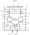
fig. 2 , an embodiment of amulticore architecture 1 corresponding to the claimed invention is shown. Thismulticore architecture 1 differs from that one infig. 1 in that aninterprocessor communication device 5 is provided. Thisinterprocessor communication device 5 links thefirst CPU 3 to thesecond CPU 4 and is configured to block interference and/or disturbance of the processes running on thefirst CPU 3 by the processes of thesecond CPU 4. The exampleinterprocessor communication device 5 enables the communication between the processors, but blocks their interference. Theinterprocessor communication device 5 is configured to grant access to the data of or on thesecond CPU 4, but it is configured to deny access to the data of or on thefirst CPU 3. Or, in other words, thefirst CPU 3 may access to the data on thesecond CPU 4, but not the other way round. Thisinterprocessor communication device 5 is also implemented onto or within the reconfigurable logic device 2 and serves merely as a (hardware) firewall between the two ormore CPUs - A detailed schematic view on the
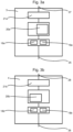
first CPU 3 is discussed with reference tofig. 3a . Thefirst CPU 3 is configured to run a first realtime operating system 18a (RTOS) and comprises a firstnetwork communication unit 19a. A first RTOS is not mandatory, but preferred. Furthermore, thefirst CPU 3 comprises aunit 20a where a safety-related application is running and carried out. This safety-related application processes the safety-related data packets which may be further processed in anencryption unit 21a offirst CPU 3. Within thisencryption unit 21a asafety layer 22 may be included to the processed safety-related data packets before they are transmitted to thehost device 11. - The
second CPU 4, according to one example of the present invention, is described with reference tofig. 3b . Thesecond CPU 4 differs from thefirst CPU 3 infig. 3a in that no safety-related application is provided. Thesecond CPU 4 instead uses aunit 20b with a non-safety-related application for processing the non-safety-related data. Therefore, it is not possible to process data packets which are categorized into any ofsafety integrity levels 1 to 4. The illustrativesecond CPU 4 also has anencryption unit 21b, but thisunit 21b may be omitted, since it is not necessary to include asafety layer 22 to the processed non-safety-related data packets. A second RTOS is not mandatory, but preferred. - Reference is made to
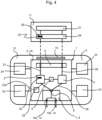
fig. 4 showing aninterface card 13 being wired or wirelessly connected to ahost device 11. Theexemplary interface card 13 comprises themulticore architecture 1 according to the embodiment shown infig. 2 . Theinterface card 13 further provides amemory 23 being connected to the reconfigurable logic device 2, i.e. the FPGA 2a.Other components 24 may be connected to the FPGA 2a, too. - A method of processing data packets comprising one or more safety-related data packets will be described in the following.
- Data packets comprising one or more safety-related data packets and one or more non-safety-related data packets are sent from a network, e.g. a train communication network to the
first input 15a and/or thesecond input 15b of the network interface module 7, which in the exemplary embodiments, is a three-port Ethernet switch 8. The data packets are split into one or more safety-related data packets and into one or more non-safety-related data packets by thedata splitting device 9 which in the preferred embodiment is formed as afiltering device 16a. - The safety-related data packets are sent via
line 25 to thefirst CPU 3 being processed there. The non-safety-related data is transmitted vialine 26 to thesecond CPU 4 being processed there. Theinterprocessor communication device 5 ensures, that the processing of the non-safety-related data within thesecond CPU 4 does not interfere the processes running on thefirst CPU 3. Thefirst CPU 3 processes safety-related data packets and thesecond CPU 4 processes non-safety-related data packets. Additionally, within thefirst encryption unit 21a of the first CPU 3 asafety layer 22 is included to the one or more processed safety-related data packets. The processed safety-related data packets are transmitted vialine 27 to thedigital interface module 6, which, may be a two channel 14digital interface module 6. Vialine 28 the processed non-safety-related data is also transmitted to thedigital interface module 6. - This
digital interface module 6 enables transmission of the processed safety-related data packets to thehost device 11, especially to ahost driver 29. Thehost driver 29 enables communication with themulticore architecture 1 and therefore with theinterface card 13. Usually thehost device 11 also comprises an operating system layer which is needed to adapt thehost driver 29 to the host target platform and, if present, the host operating system. Within the host driver 29 adecryption unit 30 is provided, that is configured to check, if thesafety layer 22 is correct and if the processed safety-related data packet is intact or not. Accordingly the processed non-safety-related data packets are also received by thehost device 11 without searching or checking for asafety layer 22. Within thehost device 11 thehost application 31 processes the data packets coming from the TCN via themulticore architecture 1. Within the host application 31 a typical control application may be running, e.g. a door control application on the train. - With the present invention it is possible to update a second real
time operating system 18b that may be within or running on the second CPU. Also the non-safety-relatedapplication 20b may be upgraded or replaced. Therefore the switch 8 may act as aprogramming port 12 being configured to communicate with thesecond CPU 4. Via thisprogramming port 12 the firmware and/or the second real time operating system within thesecond CPU 4 may be changed, updated or replaced. By use of theinterprocessor communication device 5 this updating, changing or replacing is conducted without affecting processes running on thefirst CPU 3. In a optional aspect, the new application/firmware is loaded into a memory (23a) of the FPGA 2a via the switch 8. Afterwards the new application/firmware is installed with the help of thefirst CPU 3 via theinterprocessor communication device 5 onto thesecond CPU 4. A reboot of the reconfigurable logic device 2 may be necessary afterwards. - Programming of the
interface card 13 may be performed via an Ethernet-port as described above, via a special (hardware) programming plug, or via thehost interface 10 and/or thedigital interface module 6. - The preceding description is exemplary rather than limiting in nature. Variations and modifications to the disclosed examples may be apparent to those skilled in the art. They do not necessarily depart from the essence of this invention.
-
- 1
- multicore architecture
- 2
- reconfigurable logic device
- 2a
- FPGA (field programmable gate array)
- 3
- first CPU (central processor unit / first microprocessor)
- 4
- second CPU (central processor unit / second microprocessor)
- 5
- interprocessor communication device
- 6
- digital interface module (for peripheral; e.g. for host device)
- 7
- network interface module (for network; e.g. for TCN devices)
- 8
- switch
- 9
- data splitting device
- 10
- host interface
- 11
- host device
- 12
- programming port
- 13
- interface card
- 14
- channel
- 14a
- first channel (safety-related data channel)
- 14b
- second channel (non-safety-related data channel)
- 15a
- first input
- 15b
- second input
- 16
- output port
- 16a
- filtering device
- 16b
- buffering device (for incoming data from TCN)
- 17
- board (e.g. printed board)
- 18a
- first real time operating system
- 18b
- second real time operating system
- 19a
- first network communication unit
- 19b
- second network communication unit
- 20a
- unit with safety-related application
- 20b
- unit with non-safety-related application
- 21a
- encryption unit (first CPU)
- 21b
- encryption unit (second CPU)
- 22
- safety layer
- 22*
- safety layer
- 23
- memory
- 23a
- memory (e.g. flash)
- 24
- component
- 25
- line
- 26
- line
- 27
- line
- 28
- line
- 29
- host driver
- 30
- decryption unit
- 31
- host application (unit)
Claims (10)
- A multicore architecture (1) for railway safety-related applications, the architecture comprising:a data splitting device (9) being configured to split data packets into safety-related data packets, which is all data which is categorized within one of safety integrity levels 1 to 4, and into the non-safety-related data packets, which is all data which either has no categorization or which belongs to safety integrity level 0,a logic device (2) in form of a reconfigurable field programmable gate array (FPGA) (2a);the logic device (2) including a first CPU (3) and a second CPU (4);the first CPU (3) being configured to process safety-related data packets; andthe second CPU (4) being configured to process non-safety-related data packets only,whereas an interprocessor communication device (5) is provided for linking the first CPU (3) to the second CPU (4),whereas the interprocessor communication device (5) is implemented on the reconfigurable logic device (2) itself and serves as a hardware firewall,whereas the interprocessor communication device (5) is configured to grant access to the data of or on the second CPU (4), but it is configured to deny access to the data of or on the first CPU (3), such that the first CPU (3) may access to the data on the second CPU (4), but not the other way round, and thereby blocking interference and/or disturbance of the processes running on the first CPU (3) by the processes of the second CPU (4),characterized in that the first CPU (3) comprises an encryption unit (21a) to process safety-related data packets, whereas the encryption unit (21a) is configured to include a safety layer (22) into one or more processed safety-related data packets, whereas the safety layer (22) adds a checksum and/or other information to the processed safety-related data packets enabling a host device (11) to detect if a data packet is intact or not.
- The multicore architecture (1) according to claim 1, characterized in that a digital interface module (6) is provided, the digital interface module (6) being configured to at least indirectly connect one or more peripheral devices to the first CPU (3) and/or the second CPU (4).
- The multicore architecture (1) according to claim 1 or 2, characterized in that a network interface module (7) is provided the network interface module (7) being configured to at least indirectly connect one or more network devices to the first CPU (3) and/or the second CPU (4).
- The multicore architecture (1) according to claim 3, characterized in that the network interface module (7) is formed as a multiport Ethernet switch (8).
- The multicore architecture (1) according to any of claims 1 to 4, characterized in that a host interface (10) is provided to connect at least indirectly to the first CPU (3) and/or the second CPU (4) for transmitting processed data packets to a host device (11).
- The multicore architecture (1) according to any of claims 1 to 5, characterized in that the second CPU (4) is configured to be reprogrammable, whereas the reconfigurable logic device (2) includes a memory (23a) being configured to store at least the non-safety-related data packets.
- A method of processing data packets within a multicore architecture according to any of claims 1 to 6, the data packets comprising one or more safety-related data packets, which is all data which is categorized within one of safety integrity levels 1 to 4, and one or more non-safety-related data packets, which is all data which either has no categorization or which belongs to safety integrity level 0, comprising the steps of:splitting the one or more safety-related data packets from the non-safety-related data packets by the data splitting device (9);processing the safety-related data packets in the first CPU (3) which is configured to process the safety-related data packets thereby producing one or more processed safety-related data packets having a safety layer (22) included by the encryption unit (21a) of the first CPU (3), whereas the safety layer (22) adds a checksum and/or other information to the processed safety-related data packets enabling a host device (11) to detect if a data packet is intact or not; andprocessing the one or more non-safety-related data packets in a second CPU (4) which is configured to process non-safety-related data packets only, thereby producing one or more processed non-safety-related data packets;whereas the interprocessor communication device (5) grants access to the data of or on the second CPU (4), but denies access to the data of or on the first CPU (3), such that the first CPU (3) may access to the data on the second CPU (4), but not the other way round, thereby blocking interference and/or disturbance of the processes running on the first CPU (3) by the processes of the second CPU (4).
- The method of claim 7, further including the step of:
transmitting the processed safety-related data packets to a host device (11) or a host system. - The method of any of claims 7 or 8, further comprising:providing a programming port (12) being configured to communicate with the second CPU (4); andupdating of a firmware and/or a second real time operating system within the second CPU (4) via programming port.
- An Interface card (13) being configured to link a host device (11) to a communication network, the interface card (13) comprising a multicore architecture (1) according to any of claims 1 to 6.
Priority Applications (3)
| Application Number | Priority Date | Filing Date | Title |
|---|---|---|---|
| EP17166428.7A EP3388904B1 (en) | 2017-04-13 | 2017-04-13 | Multicore architecture, interface card and method of processing data packets |
| JP2018076891A JP7160550B2 (en) | 2017-04-13 | 2018-04-12 | Multi-core architecture, interface card and method for processing data packets |
| CN201810326242.8A CN108763145B (en) | 2017-04-13 | 2018-04-12 | Multi-core architecture, interface card and method for processing data packet |
Applications Claiming Priority (1)
| Application Number | Priority Date | Filing Date | Title |
|---|---|---|---|
| EP17166428.7A EP3388904B1 (en) | 2017-04-13 | 2017-04-13 | Multicore architecture, interface card and method of processing data packets |
Publications (2)
| Publication Number | Publication Date |
|---|---|
| EP3388904A1 EP3388904A1 (en) | 2018-10-17 |
| EP3388904B1 true EP3388904B1 (en) | 2023-03-15 |
Family
ID=58632155
Family Applications (1)
| Application Number | Title | Priority Date | Filing Date |
|---|---|---|---|
| EP17166428.7A Active EP3388904B1 (en) | 2017-04-13 | 2017-04-13 | Multicore architecture, interface card and method of processing data packets |
Country Status (3)
| Country | Link |
|---|---|
| EP (1) | EP3388904B1 (en) |
| JP (1) | JP7160550B2 (en) |
| CN (1) | CN108763145B (en) |
Families Citing this family (1)
| Publication number | Priority date | Publication date | Assignee | Title |
|---|---|---|---|---|
| IT202000009592A1 (en) | 2020-04-30 | 2021-10-30 | Hitachi Rail S P A | COMMUNICATION NETWORK ARCHITECTURE FOR TRAINS |
Citations (1)
| Publication number | Priority date | Publication date | Assignee | Title |
|---|---|---|---|---|
| US7490350B1 (en) * | 2004-03-12 | 2009-02-10 | Sca Technica, Inc. | Achieving high assurance connectivity on computing devices and defeating blended hacking attacks |
Family Cites Families (10)
| Publication number | Priority date | Publication date | Assignee | Title |
|---|---|---|---|---|
| ATE550852T1 (en) * | 2000-09-29 | 2012-04-15 | Alacritech Inc | INTELLIGENT NETWORK STORAGE INTERFACE SYSTEM AND SUCH DEVICES |
| JPWO2002057921A1 (en) * | 2001-01-19 | 2004-07-22 | 株式会社日立製作所 | Electronic circuit device |
| US20030069949A1 (en) * | 2001-10-04 | 2003-04-10 | Chan Michele W. | Managing distributed network infrastructure services |
| US8055814B2 (en) * | 2005-03-18 | 2011-11-08 | Rockwell Automation Technologies, Inc. | Universal safety I/O module |
| CN101493862A (en) * | 2009-01-15 | 2009-07-29 | 北京航空航天大学 | Software and hardware cooperating design method for arithmetic acceleration |
| EP2236999B1 (en) * | 2009-04-01 | 2020-11-18 | VEGA Grieshaber KG | Field device with two processors |
| US8910177B2 (en) * | 2011-04-14 | 2014-12-09 | Advanced Micro Devices, Inc. | Dynamic mapping of logical cores |
| US8418230B1 (en) * | 2012-08-28 | 2013-04-09 | Netcomm Wireless Limited | Apparatus and method for mobile communications and computing |
| JP5862614B2 (en) * | 2013-07-11 | 2016-02-16 | 横河電機株式会社 | Field device and data processing method |
| CN104820657A (en) * | 2015-05-14 | 2015-08-05 | 西安电子科技大学 | Inter-core communication method and parallel programming model based on embedded heterogeneous multi-core processor |
-
2017
- 2017-04-13 EP EP17166428.7A patent/EP3388904B1/en active Active
-
2018
- 2018-04-12 JP JP2018076891A patent/JP7160550B2/en active Active
- 2018-04-12 CN CN201810326242.8A patent/CN108763145B/en active Active
Patent Citations (1)
| Publication number | Priority date | Publication date | Assignee | Title |
|---|---|---|---|---|
| US7490350B1 (en) * | 2004-03-12 | 2009-02-10 | Sca Technica, Inc. | Achieving high assurance connectivity on computing devices and defeating blended hacking attacks |
Non-Patent Citations (2)
| Title |
|---|
| AGIRRE IRUNE ET AL: "A Safety Concept for a Railway Mixed-Criticality Embedded System Based on Multicore Partitioning", 2015 IEEE INTERNATIONAL CONFERENCE ON COMPUTER AND INFORMATION TECHNOLOGY; UBIQUITOUS COMPUTING AND COMMUNICATIONS; DEPENDABLE, AUTONOMIC AND SECURE COMPUTING; PERVASIVE INTELLIGENCE AND COMPUTING, IEEE, 26 October 2015 (2015-10-26), pages 1780 - 1787, XP032836250, DOI: 10.1109/CIT/IUCC/DASC/PICOM.2015.268 * |
| TRUJILLO SALVADOR ET AL: "MultiPARTES: Multi-core partitioning and virtualization for easing the certification of mixed-criticality systems", MICROPROCESSORS AND MICROSYSTEMS., vol. 38, no. 8, 1 November 2014 (2014-11-01), GB, pages 921 - 932, XP055806274, ISSN: 0141-9331, DOI: 10.1016/j.micpro.2014.09.004 * |
Also Published As
| Publication number | Publication date |
|---|---|
| CN108763145A (en) | 2018-11-06 |
| CN108763145B (en) | 2023-08-18 |
| JP2018181344A (en) | 2018-11-15 |
| JP7160550B2 (en) | 2022-10-25 |
| EP3388904A1 (en) | 2018-10-17 |
Similar Documents
| Publication | Publication Date | Title |
|---|---|---|
| US10009350B2 (en) | Hardware components configured for secure physical separation of communication networks in a vehicle and methods of use thereof | |
| EP3139548B1 (en) | High assurance segregated gateway interconnecting different domains | |
| EP3074865B1 (en) | Hardware virtualization module for exclusive controlled access to cpu | |
| EP3407545B1 (en) | Evaluation device, evaluation system, and evaluation method | |
| CN104901874B (en) | High assurance security gateway interconnecting different domains | |
| CN104820626A (en) | Method for the coexistence of software having different safety levels in a multicore processor system | |
| EP2043324A1 (en) | Programmable data protection device, secure programming manager system and process for controlling access to an interconnect network for an integrated circuit. | |
| Van den Herrewegen et al. | Beneath the bonnet: A breakdown of diagnostic security | |
| WO2017009634A1 (en) | Electronic control units for vehicles | |
| EP3388904B1 (en) | Multicore architecture, interface card and method of processing data packets | |
| WO2020178089A1 (en) | Method and configurable hardware module for monitoring a hardware-application | |
| CN111033485B (en) | Method for filtering communication data arriving via a communication link in a data processing device, data processing device and motor vehicle | |
| US9973515B1 (en) | Network security for avionics with ethernet connections system and related method | |
| US11403406B2 (en) | Method and confirmation device for confirming the integrity of a system | |
| US11657183B2 (en) | Method for providing restricted access to hardware component interfaces of a network device | |
| JP2009026063A (en) | Safety control system | |
| JP2021005382A (en) | Communication device and method for authenticating message | |
| Mueller et al. | On MILS I/O sharing targeting avionic systems | |
| CN110717198B (en) | Apparatus and method for operating a processing unit built by software for a device | |
| US20150372837A1 (en) | Communication apparatus, control apparatus, and program | |
| CN116208353A (en) | Method, device, network card, chip system and server for verifying firmware | |
| EP2983088A1 (en) | Memory protection unit | |
| US10417458B2 (en) | Securing an unprotected hardware bus | |
| CN111414607A (en) | Secure element with personalizable function and corresponding management method | |
| US10491639B2 (en) | Scalable security architecture systems and methods |
Legal Events
| Date | Code | Title | Description |
|---|---|---|---|
| PUAI | Public reference made under article 153(3) epc to a published international application that has entered the european phase |
Free format text: ORIGINAL CODE: 0009012 |
|
| STAA | Information on the status of an ep patent application or granted ep patent |
Free format text: STATUS: THE APPLICATION HAS BEEN PUBLISHED |
|
| AK | Designated contracting states |
Kind code of ref document: A1 Designated state(s): AL AT BE BG CH CY CZ DE DK EE ES FI FR GB GR HR HU IE IS IT LI LT LU LV MC MK MT NL NO PL PT RO RS SE SI SK SM TR |
|
| AX | Request for extension of the european patent |
Extension state: BA ME |
|
| STAA | Information on the status of an ep patent application or granted ep patent |
Free format text: STATUS: REQUEST FOR EXAMINATION WAS MADE |
|
| 17P | Request for examination filed |
Effective date: 20190412 |
|
| RBV | Designated contracting states (corrected) |
Designated state(s): AL AT BE BG CH CY CZ DE DK EE ES FI FR GB GR HR HU IE IS IT LI LT LU LV MC MK MT NL NO PL PT RO RS SE SI SK SM TR |
|
| STAA | Information on the status of an ep patent application or granted ep patent |
Free format text: STATUS: EXAMINATION IS IN PROGRESS |
|
| 17Q | First examination report despatched |
Effective date: 20210528 |
|
| STAA | Information on the status of an ep patent application or granted ep patent |
Free format text: STATUS: EXAMINATION IS IN PROGRESS |
|
| REG | Reference to a national code |
Ref country code: DE Ref legal event code: R079 Ref document number: 602017066780 Country of ref document: DE Free format text: PREVIOUS MAIN CLASS: G05B0019040000 Ipc: G05B0019042000 |
|
| RIC1 | Information provided on ipc code assigned before grant |
Ipc: G05B 19/042 20060101AFI20220908BHEP |
|
| GRAP | Despatch of communication of intention to grant a patent |
Free format text: ORIGINAL CODE: EPIDOSNIGR1 |
|
| STAA | Information on the status of an ep patent application or granted ep patent |
Free format text: STATUS: GRANT OF PATENT IS INTENDED |
|
| INTG | Intention to grant announced |
Effective date: 20221018 |
|
| GRAS | Grant fee paid |
Free format text: ORIGINAL CODE: EPIDOSNIGR3 |
|
| GRAA | (expected) grant |
Free format text: ORIGINAL CODE: 0009210 |
|
| STAA | Information on the status of an ep patent application or granted ep patent |
Free format text: STATUS: THE PATENT HAS BEEN GRANTED |
|
| AK | Designated contracting states |
Kind code of ref document: B1 Designated state(s): AL AT BE BG CH CY CZ DE DK EE ES FI FR GB GR HR HU IE IS IT LI LT LU LV MC MK MT NL NO PL PT RO RS SE SI SK SM TR |
|
| REG | Reference to a national code |
Ref country code: CH Ref legal event code: EP Ref country code: GB Ref legal event code: FG4D |
|
| REG | Reference to a national code |
Ref country code: DE Ref legal event code: R096 Ref document number: 602017066780 Country of ref document: DE |
|
| REG | Reference to a national code |
Ref country code: IE Ref legal event code: FG4D |
|
| REG | Reference to a national code |
Ref country code: AT Ref legal event code: REF Ref document number: 1554355 Country of ref document: AT Kind code of ref document: T Effective date: 20230415 |
|
| REG | Reference to a national code |
Ref country code: LT Ref legal event code: MG9D |
|
| P01 | Opt-out of the competence of the unified patent court (upc) registered |
Effective date: 20230530 |
|
| REG | Reference to a national code |
Ref country code: NL Ref legal event code: MP Effective date: 20230315 |
|
| PG25 | Lapsed in a contracting state [announced via postgrant information from national office to epo] |
Ref country code: RS Free format text: LAPSE BECAUSE OF FAILURE TO SUBMIT A TRANSLATION OF THE DESCRIPTION OR TO PAY THE FEE WITHIN THE PRESCRIBED TIME-LIMIT Effective date: 20230315 Ref country code: NO Free format text: LAPSE BECAUSE OF FAILURE TO SUBMIT A TRANSLATION OF THE DESCRIPTION OR TO PAY THE FEE WITHIN THE PRESCRIBED TIME-LIMIT Effective date: 20230615 Ref country code: LV Free format text: LAPSE BECAUSE OF FAILURE TO SUBMIT A TRANSLATION OF THE DESCRIPTION OR TO PAY THE FEE WITHIN THE PRESCRIBED TIME-LIMIT Effective date: 20230315 Ref country code: LT Free format text: LAPSE BECAUSE OF FAILURE TO SUBMIT A TRANSLATION OF THE DESCRIPTION OR TO PAY THE FEE WITHIN THE PRESCRIBED TIME-LIMIT Effective date: 20230315 Ref country code: HR Free format text: LAPSE BECAUSE OF FAILURE TO SUBMIT A TRANSLATION OF THE DESCRIPTION OR TO PAY THE FEE WITHIN THE PRESCRIBED TIME-LIMIT Effective date: 20230315 |
|
| PGFP | Annual fee paid to national office [announced via postgrant information from national office to epo] |
Ref country code: FR Payment date: 20230504 Year of fee payment: 7 Ref country code: DE Payment date: 20230403 Year of fee payment: 7 |
|
| REG | Reference to a national code |
Ref country code: AT Ref legal event code: MK05 Ref document number: 1554355 Country of ref document: AT Kind code of ref document: T Effective date: 20230315 |
|
| PG25 | Lapsed in a contracting state [announced via postgrant information from national office to epo] |
Ref country code: SE Free format text: LAPSE BECAUSE OF FAILURE TO SUBMIT A TRANSLATION OF THE DESCRIPTION OR TO PAY THE FEE WITHIN THE PRESCRIBED TIME-LIMIT Effective date: 20230315 Ref country code: NL Free format text: LAPSE BECAUSE OF FAILURE TO SUBMIT A TRANSLATION OF THE DESCRIPTION OR TO PAY THE FEE WITHIN THE PRESCRIBED TIME-LIMIT Effective date: 20230315 Ref country code: GR Free format text: LAPSE BECAUSE OF FAILURE TO SUBMIT A TRANSLATION OF THE DESCRIPTION OR TO PAY THE FEE WITHIN THE PRESCRIBED TIME-LIMIT Effective date: 20230616 Ref country code: FI Free format text: LAPSE BECAUSE OF FAILURE TO SUBMIT A TRANSLATION OF THE DESCRIPTION OR TO PAY THE FEE WITHIN THE PRESCRIBED TIME-LIMIT Effective date: 20230315 |
|
| P02 | Opt-out of the competence of the unified patent court (upc) changed |
Effective date: 20230807 |
|
| PG25 | Lapsed in a contracting state [announced via postgrant information from national office to epo] |
Ref country code: SM Free format text: LAPSE BECAUSE OF FAILURE TO SUBMIT A TRANSLATION OF THE DESCRIPTION OR TO PAY THE FEE WITHIN THE PRESCRIBED TIME-LIMIT Effective date: 20230315 Ref country code: RO Free format text: LAPSE BECAUSE OF FAILURE TO SUBMIT A TRANSLATION OF THE DESCRIPTION OR TO PAY THE FEE WITHIN THE PRESCRIBED TIME-LIMIT Effective date: 20230315 Ref country code: PT Free format text: LAPSE BECAUSE OF FAILURE TO SUBMIT A TRANSLATION OF THE DESCRIPTION OR TO PAY THE FEE WITHIN THE PRESCRIBED TIME-LIMIT Effective date: 20230717 Ref country code: ES Free format text: LAPSE BECAUSE OF FAILURE TO SUBMIT A TRANSLATION OF THE DESCRIPTION OR TO PAY THE FEE WITHIN THE PRESCRIBED TIME-LIMIT Effective date: 20230315 Ref country code: EE Free format text: LAPSE BECAUSE OF FAILURE TO SUBMIT A TRANSLATION OF THE DESCRIPTION OR TO PAY THE FEE WITHIN THE PRESCRIBED TIME-LIMIT Effective date: 20230315 Ref country code: CZ Free format text: LAPSE BECAUSE OF FAILURE TO SUBMIT A TRANSLATION OF THE DESCRIPTION OR TO PAY THE FEE WITHIN THE PRESCRIBED TIME-LIMIT Effective date: 20230315 Ref country code: AT Free format text: LAPSE BECAUSE OF FAILURE TO SUBMIT A TRANSLATION OF THE DESCRIPTION OR TO PAY THE FEE WITHIN THE PRESCRIBED TIME-LIMIT Effective date: 20230315 |
|
| PG25 | Lapsed in a contracting state [announced via postgrant information from national office to epo] |
Ref country code: SK Free format text: LAPSE BECAUSE OF FAILURE TO SUBMIT A TRANSLATION OF THE DESCRIPTION OR TO PAY THE FEE WITHIN THE PRESCRIBED TIME-LIMIT Effective date: 20230315 Ref country code: PL Free format text: LAPSE BECAUSE OF FAILURE TO SUBMIT A TRANSLATION OF THE DESCRIPTION OR TO PAY THE FEE WITHIN THE PRESCRIBED TIME-LIMIT Effective date: 20230315 Ref country code: IS Free format text: LAPSE BECAUSE OF FAILURE TO SUBMIT A TRANSLATION OF THE DESCRIPTION OR TO PAY THE FEE WITHIN THE PRESCRIBED TIME-LIMIT Effective date: 20230715 |
|
| REG | Reference to a national code |
Ref country code: CH Ref legal event code: PL |
|
| REG | Reference to a national code |
Ref country code: DE Ref legal event code: R097 Ref document number: 602017066780 Country of ref document: DE |
|
| PG25 | Lapsed in a contracting state [announced via postgrant information from national office to epo] |
Ref country code: LU Free format text: LAPSE BECAUSE OF NON-PAYMENT OF DUE FEES Effective date: 20230413 |
|
| REG | Reference to a national code |
Ref country code: BE Ref legal event code: MM Effective date: 20230430 |
|
| PG25 | Lapsed in a contracting state [announced via postgrant information from national office to epo] |
Ref country code: MC Free format text: LAPSE BECAUSE OF FAILURE TO SUBMIT A TRANSLATION OF THE DESCRIPTION OR TO PAY THE FEE WITHIN THE PRESCRIBED TIME-LIMIT Effective date: 20230315 |
|
| PLBE | No opposition filed within time limit |
Free format text: ORIGINAL CODE: 0009261 |
|
| STAA | Information on the status of an ep patent application or granted ep patent |
Free format text: STATUS: NO OPPOSITION FILED WITHIN TIME LIMIT |
|
| PG25 | Lapsed in a contracting state [announced via postgrant information from national office to epo] |
Ref country code: SI Free format text: LAPSE BECAUSE OF FAILURE TO SUBMIT A TRANSLATION OF THE DESCRIPTION OR TO PAY THE FEE WITHIN THE PRESCRIBED TIME-LIMIT Effective date: 20230315 Ref country code: MC Free format text: LAPSE BECAUSE OF FAILURE TO SUBMIT A TRANSLATION OF THE DESCRIPTION OR TO PAY THE FEE WITHIN THE PRESCRIBED TIME-LIMIT Effective date: 20230315 Ref country code: LI Free format text: LAPSE BECAUSE OF NON-PAYMENT OF DUE FEES Effective date: 20230430 Ref country code: DK Free format text: LAPSE BECAUSE OF FAILURE TO SUBMIT A TRANSLATION OF THE DESCRIPTION OR TO PAY THE FEE WITHIN THE PRESCRIBED TIME-LIMIT Effective date: 20230315 Ref country code: CH Free format text: LAPSE BECAUSE OF NON-PAYMENT OF DUE FEES Effective date: 20230430 |
|
| REG | Reference to a national code |
Ref country code: IE Ref legal event code: MM4A |
|
| 26N | No opposition filed |
Effective date: 20231218 |
|
| GBPC | Gb: european patent ceased through non-payment of renewal fee |
Effective date: 20230615 |
|
| PG25 | Lapsed in a contracting state [announced via postgrant information from national office to epo] |
Ref country code: BE Free format text: LAPSE BECAUSE OF NON-PAYMENT OF DUE FEES Effective date: 20230430 |
|
| PG25 | Lapsed in a contracting state [announced via postgrant information from national office to epo] |
Ref country code: IE Free format text: LAPSE BECAUSE OF NON-PAYMENT OF DUE FEES Effective date: 20230413 |