EP3386103A1 - Digital filter, filter processing method, and recording medium - Google Patents
Digital filter, filter processing method, and recording medium Download PDFInfo
- Publication number
- EP3386103A1 EP3386103A1 EP16870761.0A EP16870761A EP3386103A1 EP 3386103 A1 EP3386103 A1 EP 3386103A1 EP 16870761 A EP16870761 A EP 16870761A EP 3386103 A1 EP3386103 A1 EP 3386103A1
- Authority
- EP
- European Patent Office
- Prior art keywords
- signal
- complex
- filter
- circuit
- complex signal
- Prior art date
- Legal status (The legal status is an assumption and is not a legal conclusion. Google has not performed a legal analysis and makes no representation as to the accuracy of the status listed.)
- Granted
Links
Images




Classifications
-
- H—ELECTRICITY
- H03—ELECTRONIC CIRCUITRY
- H03H—IMPEDANCE NETWORKS, e.g. RESONANT CIRCUITS; RESONATORS
- H03H17/00—Networks using digital techniques
- H03H17/02—Frequency selective networks
- H03H17/0201—Wave digital filters
-
- G—PHYSICS
- G06—COMPUTING OR CALCULATING; COUNTING
- G06F—ELECTRIC DIGITAL DATA PROCESSING
- G06F17/00—Digital computing or data processing equipment or methods, specially adapted for specific functions
- G06F17/10—Complex mathematical operations
- G06F17/15—Correlation function computation including computation of convolution operations
-
- H—ELECTRICITY
- H03—ELECTRONIC CIRCUITRY
- H03H—IMPEDANCE NETWORKS, e.g. RESONANT CIRCUITS; RESONATORS
- H03H17/00—Networks using digital techniques
- H03H17/02—Frequency selective networks
Definitions
- the present invention relates to arithmetic processing in digital signal processing, and more particularly, to a digital filter, a filter processing method, and a filter processing program.
- PTL 1 discloses the following filter processing method by a digital filter.
- a digital filter transforms a complex signal in a time domain into a first complex signal in a frequency domain by Fourier transform.
- a second complex signal including respective complex conjugates of all complex numbers constituting the first complex signal is generated.
- filter processing by a predetermined frequency-domain filter coefficient is performed on each of the first complex signal and the second complex signal.
- the first complex signal after filter processing, and the second complex signal after filter processing are combined, and a complex signal in a frequency domain after filter processing is generated.
- inverse Fourier transform is performed on the complex signal in a frequency domain after filter processing, and a time-domain complex signal after filter processing is acquired.
- PTL 1 discloses the following method for generating a frequency-domain filter coefficient by a filter coefficient generation means. Specifically, the filter coefficient generation means generates the frequency-domain filter coefficient by adding a second input filter coefficient to a first input filter coefficient by complex addition, and then, multiplying the third input filter coefficient with a complex multiplication. Further, the filter coefficient generation means generates a second frequency-domain filter coefficient by subtracting the second input filter coefficient from a first input filter coefficient by complex subtraction, and then, multiplying the result by the third input filter coefficient by complex multiplication.
- PTL 2 discloses a digital filter circuit including a Fourier transform means, an IQ separation means, two filter means, an IQ combining means, a third filter means, and an inverse Fourier transform means.
- PTL 3 discloses a signal processing device including a discrete Fourier transform unit, a vector multiplication circuit, and an inverse discrete Fourier transform unit.
- PTL 4 discloses a fast Fourier transform processing device for performing predetermined arithmetic processing.
- the digital filter disclosed in PTL 1 performs filter processing on a second complex signal, and a third complex signal being conjugate of the second complex signal, which are generated from a first complex signal by a complex separation unit. Since the second complex signal and the third complex signal have predetermined signal amplitudes, there is a problem that power consumption required for filter processing, and an amount of heat generated when filter processing is performed are large.
- An object of the present invention is to solve the problem described above, and to provide a digital filter and the like, which can increase a possibility that power consumption required for filter processing, and an amount of heat generated when filter processing is performed can be reduced.
- a digital filter includes a separation unit, a signal selection unit, a first filter unit, a second filter unit, and a combining unit.
- the separation unit generates, from a first complex signal in a frequency domain output to the separation unit, a second complex signal and a third complex signal being a complex conjugate of the second complex signal.
- the separation unit outputs the second complex signal and the third complex signal to the signal selection unit.
- the signal selection unit performs switching by selecting, from among a plurality of types of complex signals having different amounts of change in signal amplitude, by using the second complex signal and the third complex signal output to the signal selection unit by the separation unit.
- the signal selection unit performs the switching with respect to at least one of a fourth complex signal to be output to the first filter unit and a fifth complex signal to be output to the second filter unit by the signal selection unit.
- the first filter unit performs filter processing on the fourth complex signal by a first filter coefficient, and generates a sixth complex signal.
- the first filter unit outputs the sixth complex signal to the combining unit.
- the second filter unit performs processing on the fifth complex signal by a second filter coefficient, and generates a seventh complex signal.
- the second filter unit outputs the seventh complex signal to the combining unit.
- the combining unit combines the sixth complex signal and the seventh complex signal, and generates and outputs an eighth complex signal being a complex signal after combining.
- the digital filter and the like according to the present invention are able to increase a possibility that power consumption required for filter processing, and an amount of heat generated when filter processing is performed can be reduced.
- Fig. 1 is a conceptual diagram illustrating a configuration of a digital filter circuit 10 being an example of a digital filter circuit according to a first example embodiment. Further, Fig. 2 is a sequence chart illustrating an operation example to be performed by the digital filter circuit 10.
- the digital filter circuit 10 includes an FT circuit 13, an IFT circuit 14, a separation circuit 15, and a combining circuit 16.
- FT means Fourier transform
- IFT means inverse Fourier transform
- the digital filter circuit 10 further includes a filter circuit 21, a filter circuit 22, a filter coefficient generation circuit 41, and a filter coefficient generation circuit 42.
- the FT circuit 13 performs the following operation illustrated in S101 in Fig. 2 .
- the FT circuit 13 performs FT on the input complex signal x(n), and generates a complex signal X(k) in a frequency domain.
- X k R k + jS k
- n is an integer representing a signal sample number in a time domain: 0 ⁇ n ⁇ N-1
- N is an integer representing a transform sample number of FT: 0 ⁇ N
- k is an integer representing a frequency number in a frequency domain: 0 ⁇ k ⁇ N-1.
- the FT circuit 13 generates a complex signal X(N-k) from the complex signal X(k).
- X N ⁇ k R N ⁇ k + jS N ⁇ K
- the FT circuit 13 outputs a complex signal i31 including the complex signal X(k) and the complex signal X(N-k) to the separation circuit 15 and a signal selection circuit 19.
- FFT fast Fourier transform
- the separation circuit 15 performs the following operation illustrated in S102 in Fig. 2 .
- the separation circuit 15 generates an I component signal XI(k) and a Q component signal XQ(k) being a pair of complex conjugates of X(k) as will be described later, by using the complex signal X(k) and the complex signal X(N-k) output to the separation circuit 15 by the FT circuit 13.
- the separation circuit 15 further generates an I component signal XI(k)
- the separation circuit 15 outputs a complex signal i32 including the generated I component signal XI(k) and the generated Q component signal XQ(k) to the signal selection circuit 19.
- the signal selection circuit 19 performs the following operation illustrated in S103 in Fig. 2 .
- a selection signal i48 is input to the signal selection circuit 19.
- the selection signal i48 is supplied from a part constituting a host device of the digital filter circuit 10, for example.
- the signal selection circuit 19 performs signal selection based on a selection mode included in the selection signal i48.
- the selection signal i48 is a signal including a content designating one of a first selection mode and a second selection mode.
- the signal selection circuit 19 When the selection signal i48 includes a content designating the first selection mode, the signal selection circuit 19 performs selection of an output signal to the filter circuits 21 and 22 based on the first selection mode. When the signal selection circuit 19 performs selection of an output signal to the filter circuits 21 and 22 based on the first selection mode, the digital filter circuit 10 performs filter processing based on the first selection mode.
- the signal selection circuit 19 performs selection of an output signal to the filter circuits 21 and 22 based on the second selection mode.
- the digital filter circuit 10 performs filter processing based on the second selection mode.
- the signal selection circuit 19 When the selection mode is the first selection mode, the signal selection circuit 19 outputs, to the filter circuit 21, the complex signal i32 including the I component signal XI(k) expressed by Eq. (5). Further, the signal selection circuit 19 outputs, to the filter circuit 22, a complex signal i33 including the Q component signal XQ(k) expressed by Eq. (6).
- the signal selection circuit 19 outputs, to the filter circuit 21, the complex signal i32 including the I component signal XI(k) expressed by Eq. (5'). Further, the signal selection circuit 19 outputs, to the filter circuit 22, the complex signal i33 including the Q component signal XQ(k) expressed by Eq. (6').
- the filter coefficient generation circuit 41 performs the following operation illustrated in S104 in Fig. 2 .
- a complex coefficient V(k) and a complex coefficient H(k) are output to the filter coefficient generation circuit 41.
- the output is performed by a part constituting a host device of the digital filter circuit 10, for example.
- the filter coefficient generation circuit 41 generates a filter coefficient CI(k) from the complex coefficients V(k) and H(k) output to the filter coefficient generation circuit 41 by an external unit, regarding each frequency number k: 0 ⁇ k ⁇ N-1.
- CI k V k ⁇ H k
- the filter coefficient generation circuit 42 performs the following operation illustrated in S105 in Fig. 2 .
- Complex coefficients W(k) and H(k) are output to the filter coefficient generation circuit 42.
- the output is performed by a part constituting a host device of the digital filter circuit 10, for example.
- the filter coefficient circuit 42 generates a complex coefficient from the input complex coefficients W(k) and H(k), regarding each frequency number k: 0 ⁇ k ⁇ N-1.
- CQ k W k ⁇ H k
- V(k), W(k), and H(k) are coefficients in a frequency domain, which are associated with a real filter coefficient when filter processing by real number operation is performed in a time domain. Details on V(k), W(k), and H(k) will be described later.
- the filter coefficient generation circuit 41 includes the generated filter coefficient CI(k) in a complex signal i45, and outputs the complex signal i45 to the filter circuit 21. Further, the filter coefficient generation circuit 42 includes the generated filter coefficient CQ(k) in a complex signal i46, and outputs the complex signal i46 to the filter circuit 22.
- the filter circuit 21 performs the following operation illustrated in S106 in Fig. 2 .
- the filter circuit 21 performs complex filter processing by complex multiplication on the I component signal XI(k) included in the complex signal i32 output to the filter circuit 21 by the signal selection unit.
- the filter circuit 21 uses the filter coefficient CI(k) included in the complex signal i45 output to the filter circuit 21 by the filter coefficient generation circuit 41, when the complex filter processing is performed.
- the filter circuit 21 calculates a complex signal XI' regarding each frequency number k: 0 ⁇ k ⁇ N-1, and outputs a complex signal i34 including the complex signal XI' to the combining circuit 16.
- XI ′ k XI k ⁇ CI k
- the filter circuit 22 performs the following operation illustrated in S107 in Fig. 2 .
- the filter circuit 22 performs complex filter processing by complex multiplication on the Q component signal XQ(k) included in the complex signal i33 output to the filter circuit 22 by the signal selection unit 19.
- the filter circuit 22 uses the filter coefficient CQ(k) included in the complex signal i46 output to the filter circuit 22 by the filter coefficient generation circuit 42, when complex filter processing by the complex multiplication is performed.
- the filter circuit 22 calculates a complex signal XQ'(k) regarding each frequency number k: 0 ⁇ k ⁇ N-1, and outputs a complex signal i35 including the complex signal XQ'(k) to the combining circuit 16.
- XQ ′ k XQ k ⁇ CQ k
- the combining circuit 16 performs the following operation illustrated in S108 in Fig. 2 .
- the combining circuit 16 generates a complex signal X"(k), which is acquired by combining the complex signal XI'(k) expressed by Eq. (9) and the complex signal XQ'(k) expressed by Eq. (10).
- the complex signal XI'(k) is a complex signal included in the complex signal i34 to be output to the combining circuit 16 by the filter circuit 21.
- the complex signal XQ'(k) is a complex signal included in the complex signal i35 to be output to the combining circuit 16 by the filter circuit 22.
- the combining unit 16 calculates the complex signal X"(k) regarding each frequency number k: 0 ⁇ k ⁇ N-1, and outputs a complex signal i36 including the complex signal X"(k) to the IFT circuit 14.
- X " k XI ′ k + XQ ′ k
- the combining circuit 16 performs the following operation illustrated in S109 in Fig. 2 .
- the IFT circuit 14 performs inverse Fourier transform (hereinafter, referred to as "IFT") on the complex signal X"(k) (see Eq. (13)) included in the complex signal i36 to be output to the IFT circuit 14 by the combining unit 16, regarding each frequency number k: ⁇ 0 ⁇ k ⁇ N-1. Further, the IFT circuit 14 generates a complex signal x"(n) in a time domain by the IFT. The IFT circuit 14 further outputs a signal y(n) including the complex signal x"(n) to an external unit of the unillustrated digital filter circuit 10.
- IFT inverse Fourier transform
- Fig. 3 is a conceptual diagram illustrating a configuration example of the separation unit 15 being an example of a separation circuit.
- lines indicating signal paths illustrated in Fig. 3 solid lines indicate signal paths of real parts of signals, and dotted lines indicate signal paths of imaginary parts of the signals.
- the separation circuit 15 includes adder circuits 150 and 152, subtraction circuits 151 and 153, and multiplication circuits 154 to 158.
- Complex signals X(k) and X(N-k) are input to the separation circuit 15.
- the complex signals X(k) and X(N-k) are complex signals included in the complex signal i31 to be transmitted to the separation circuit 15 by the FT circuit 13, which is described with reference to Fig. 1 .
- a real part R(k) of the complex signal X(k) input to the separation circuit 15 is input to a terminal 121a.
- An imaginary part S(k) of the complex signal X(k) input to the separation circuit 15 is input to a terminal 121b.
- R(N-k) of the complex signal X(N-k) input to the separation circuit 15 is input to a terminal 121c.
- R(N-k) is also a real part of a complex conjugate X*(N-k) of the complex signal X(N-k).
- An imaginary part S(N-k) of the complex signal X(N-k) input to the separation circuit 15 is input to a terminal 121d.
- the separation circuit 15 includes an unillustrated separation circuit for separating the complex signal i31.
- the separation circuit separates, from the complex signal i31, the real part R(k) of the complex signal X(k), the imaginary part S(k) of the complex signal X(k), the real part R(N-k) of the complex signal X(N-k), and the imaginary part S(N-k) of the complex signal X(N-k). Further, the separation circuit outputs the real part R(k) of the complex signal X(k) to the terminal 121a, and outputs the imaginary part S(k) of the complex signal X(k) to the terminal 121b. The separation circuit further outputs the real part R(N-k) of the complex signal X(N-k) to the terminal 121c, and outputs the imaginary part S(N-k) of the complex signal X(N-k) to the terminal 121d.
- the real part R(k) of the complex signal X(k) input to the terminal 121a is transmitted to the adder circuit 150 and the subtraction circuit 153.
- the imaginary part S(k) of the complex signal X(k) input to the terminal 121b is transmitted to the adder circuit 152 and the subtraction circuit 151.
- the real part R(N-k) of the complex signal X(N-k) input to the terminal 121c is transmitted to the adder circuit 150 and the subtraction circuit 153.
- the imaginary part S(N-k) of the complex signal X(N-k) input to the terminal 121d is transmitted to the adder circuit 152 and the subtraction circuit 151.
- the multiplication circuit 158 multiplies the imaginary part S(N-k) transmitted to the multiplication circuit 158 by a value of -1, and acquires an imaginary part -S(N-k).
- the imaginary part -S(N-k) is an imaginary part of the complex conjugate X*(N-k) of the complex signal X(N-k).
- the multiplication circuit 158 transmits -S(N-k) to the adder circuit 152 and the subtraction circuit 151.
- the adder circuit 150 adds the real part R(k) transmitted from the terminal 121a and the real part R(N-k) transmitted from the terminal 121c, and acquires a real part R(k)+R(N-k).
- the adder circuit 150 transmits the real part R(k)+R(N-k) to the multiplication circuit 154.
- the multiplication circuit 154 multiplies the real part R(k)+R(N-k) transmitted from the adder circuit 150 by a value of 1/2, and acquires a real part (R(k)+R(N-k))/2.
- the multiplication circuit 154 transmits the real part (R(k)+R(N-k))/2 to the signal selection circuit 19 illustrated in Fig. 1 through a terminal 121e.
- the adder circuit 152 adds the imaginary part S(k) transmitted from the terminal 121b and the imaginary part -S(N-k) transmitted to the adder circuit 152 by the multiplication circuit 158, and acquires an imaginary part S(k)-S(N-k).
- the adder circuit 152 transmits the imaginary part S(k)-S(N-k) to the multiplication circuit 155.
- the multiplication circuit 155 multiplies the imaginary part S(k)-S(N-k) transmitted from the adder circuit 152 by a value of 1/2, and acquires an imaginary part (S(k)-S(N-k))/2.
- the multiplication circuit 155 transmits the imaginary part (S(k)-S(N-k))/2 to the signal selection circuit 19 illustrated in Fig. 1 through a terminal 121f.
- the subtraction circuit 153 subtracts the real part R(N-k) transmitted to the subtraction circuit 153 by the separation circuit 113, from the real part R(k) transmitted from the terminal 121a, and acquires a real part R(k)-R(N-k).
- the subtraction circuit 153 transmits the real part R(k)-R(N-k) to the multiplication circuit 156.
- the multiplication circuit 156 multiplies the real part R(k)-R(N-k) transmitted to the multiplication circuit 156 by the subtraction circuit 153 by a value of 1/2, and acquires a real part (R(k)-R(N-k))/2.
- the multiplication circuit 156 transmits the real part (R(k)-R(N-k))/2 to the signal selection circuit 19 illustrated in Fig. 1 through a terminal 121g.
- the subtraction circuit 151 subtracts the imaginary part -S(N-k) transmitted to the subtraction circuit 151 by the multiplication circuit 158, from the imaginary part S(k) transmitted from the terminal 121b, and acquires an imaginary part S(k)+S(N-k).
- the subtraction circuit 151 transmits the imaginary part S(k)+S(N-k) to the multiplication circuit 157.
- the multiplication circuit 157 multiplies the imaginary part S(k)+S(N-k) transmitted to the multiplication circuit 157 by the subtraction circuit 151, and acquires an imaginary part (S(k)+S(N-k))/2.
- the multiplication circuit 157 transmits the imaginary part (S(k)+S(N-k))/2 to the signal selection circuit 19 illustrated in Fig. 1 through a terminal 121 h.
- the separation circuit 15 performs an operation of separating an input complex signal into the I component signal XI(k) and the Q component signal XQ(k), and outputting to the signal selection circuit 19.
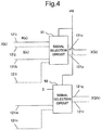
- Fig. 4 is a conceptual diagram illustrating a configuration example of the signal selection circuit 19.
- the signal selection circuit 19 includes a signal selection circuit 51 and a signal selection circuit 52.
- the real part R(k) of the complex signal X(k) is input to the signal selection circuit 51 through a terminal 121i.
- the imaginary part S(k) of the complex signal X(k) is input to the signal selection circuit 51 through a terminal 121j.
- the complex signal X(k) is the complex signal X(k) included in the complex signal i31 output to the signal selection circuit 19 by the FT circuit 13 illustrated in Fig. 1 .
- the real part (R(k)+R(N-k))/2 is input to the signal selection circuit 51 through a terminal 121k.
- the real part (R(k)+R(N-k))/2 is the real part (R(k)+R(N-k))/2 to be transmitted to the signal selection circuit 19 by the multiplication circuit 154 of the separation circuit 15 illustrated in Fig. 3 through the terminal 121e.
- the real part (R(k)-R(N-k))/2 is input to the signal selection circuit 51 through a terminal 1211.
- the real part (R(k)-R(N-k))/2 is the real part (R(k)-R(N-k))/2 to be transmitted to the signal selection circuit 19 by the multiplication circuit 156 of the separation circuit 15 illustrated in Fig. 3 through the terminal 121g.
- the imaginary part (S(k)-S(N-k))/2 is input to the signal selection circuit 52 through a terminal 121m.
- the imaginary part (S(k)-S(N-k))/2 is the imaginary part (S(k)-S(N-k))/2 to be transmitted to the signal selection circuit 19 by the multiplication circuit 155 of the separation circuit 15 illustrated in Fig. 3 through the terminal 121f.
- the imaginary part (S(k)+S(N-k))/2 is input to the signal selection circuit 52 through a terminal 121n.
- the imaginary part (S(k)+S(N-k))/2 is the imaginary part (S(k)+S(N-k))/2 to be transmitted to the signal selection circuit 19 by the multiplication circuit 157 of the separation circuit 15 illustrated in Fig. 3 through the terminal 121h.
- the signal selection circuit 51 holds the complex signal X(k) and the I component signal XI(k).
- the complex signal X(k) is the I component signal XI(k) expressed by Eq. (5').
- the I component signal XI(k) transmitted to the signal selection circuit 51 by a combining circuit 122 is the I component signal XI(k) expressed by Eq. (5).
- the selection signal i48 to be input to the signal selection circuit 19 is input to the signal selection circuits 51 and 52.
- the selection signal i48 is the selection signal i48 to be output to the signal selection circuit 19 by an external unit of the digital filter circuit 10, which has been described with reference to Fig. 1 .
- the signal selection circuit 51 When the selection mode included in the selection signal i48 input to the signal selection circuit 51 is a selection mode 1, the signal selection circuit 51 outputs the I component signal XI(k) expressed by Eq. (5) to the filter circuit 21 illustrated in Fig. 1 . Specifically, the signal selection circuit 51 outputs a real part of the I component signal XI(k) from the terminal 121e, and outputs an imaginary part of the I component signal XI(k) from the terminal 121f to the filter circuit 21 illustrated in Fig. 1 . The signal selection circuit 51 may output the I component signal XI(k) as it is to the filter circuit 21 illustrated in Fig. 1 , as the signal i32 illustrated in Fig. 1 .
- the signal selection circuit 51 may include an unillustrated combining circuit at a post stage of the terminal 121e and the terminal 121f. Further, the combining circuit may output a signal acquired by combining a real part of the I component signal XI(k) and an imaginary part of the I component signal XI(k) to the filter circuit 21 illustrated in Fig. 1 , as the signal i32 illustrated in Fig. 1 .
- a description on an operation of the signal selection circuit 51 when the selection mode included in the selection signal i48 is a selection mode 2 is a description in which Eq. (5) is read as Eq. (5') in the description on an operation of the signal selection circuit 51.
- the signal selection circuit 52 When the selection mode included in the selection signal i48 input to the signal selection circuit 52 is the selection mode 1, the signal selection circuit 52 outputs the complex signal X(k) expressed by Eq. (6) to the filter circuit 22, as the Q component signal XQ(k) . Specifically, the signal selection circuit 52 outputs a real part of the Q component signal XQ(k) from the terminal 121g, and outputs an imaginary part of the Q component signal XQ(k) from the terminal 121h to the filter circuit 22 illustrated in Fig. 1 . The signal selection circuit 52 may output the Q component signal XQ(k) to the filter circuit 22 illustrated in Fig. 1 , as the complex signal i33 illustrated in Fig. 1 .
- the signal selection circuit 52 may include an unillustrated combining circuit at a post stage of the terminal 121g and the terminal 121h. Further, the combining circuit may output a signal acquired by combining a real part of the Q component signal XQ(k) and an imaginary part of the Q component signal XQ(k) to the filter circuit 22 illustrated in Fig. 1 , as the complex signal i33 illustrated in Fig. 1 .
- a description on an operation of the signal selection circuit 52 when the selection mode included in the selection signal i48 is the selection mode 2 is a description in which Eq. (6) is read as Eq. (6') in the description on an operation of the signal selection circuit 52.
- Fig. 5 is a conceptual diagram illustrating a configuration example of the filter coefficient generation circuit 41 being a first filter coefficient generation circuit.
- solid lines indicate signal paths of real parts of signals
- dotted lines indicate signal paths of imaginary parts of the signals.
- the filter coefficient generation circuit 41 includes multiplication circuits 169a to 172a, an adder circuit 164a, and a subtraction circuit 165a.
- Complex coefficients V(k) and H(k) are input to the filter coefficient generation circuit 41.
- the complex coefficients V(k) and H(k) are the complex coefficients V(k) and H(k) to be input to the filter coefficient generation circuit 41, which has been described with reference to Fig. 1 .
- a real part VI(k) of the complex coefficient V(k) input to the filter coefficient generation circuit 41 is input to a terminal 122a.
- An imaginary part VQ(k) of the complex coefficient V(k) input to the filter coefficient generation circuit 41 is input to a terminal 122b.
- a real part HI(k) of the complex coefficient H(k) input to the filter coefficient generation circuit 41 is input to a terminal 122c.
- An imaginary part HQ(k) of the complex coefficient H(k) input to the filter coefficient generation circuit 41 is input to a terminal 122d.
- the filter coefficient generation circuit 41 When the complex coefficient V(k) to be input to the filter coefficient generation circuit 41 is input through one signal line, the filter coefficient generation circuit 41 includes an unillustrated separation circuit for separating the complex coefficient V(k).
- the separation circuit separates, from the complex coefficient V(k), the real part VI(k) of the complex coefficient V(k) and the imaginary part VQ(k) of the complex coefficient V(k). Further, the separation circuit inputs the real part VI(k) of the complex coefficient V(k) to the terminal 122a, and inputs the imaginary part VQ(k) of the complex coefficient V(k) to the terminal 122b.
- the filter coefficient generation circuit 41 includes an unillustrated separation circuit for separating the complex coefficient H(k).
- the separation circuit separates, from the complex coefficient H(k), the real part HI(k) of the complex coefficient H(k) and the imaginary part HQ(k) of the complex coefficient H(k). Further, the separation circuit outputs the real part HI(k) of the complex coefficient H(k) to the terminal 122c, and outputs the imaginary part HQ(k) of the complex coefficient H(k) to the terminal 122d.
- the real part VI(k) of the complex coefficient V(k) input to the terminal 122a is transmitted to the multiplication circuit 169a and the multiplication circuit 171a.
- the imaginary part VQ(k) of the complex coefficient V(k) input to the terminal 122b is transmitted to the multiplication circuit 170a and the multiplication circuit 172a.
- the real part HI(k) of the complex coefficient H(k) input to the terminal 122c is transmitted to the multiplication circuit 169a and the multiplication circuit 172a.
- the imaginary part HQ(k) of the complex coefficient H(k) input to the terminal 122d is transmitted to the multiplication circuit 171a and the multiplication circuit 172a.
- the multiplication circuit 169a multiplies the real part VI(k) of the complex coefficient V(k) transmitted from the terminal 122a by the real part HI(k) of the complex coefficient H(k) transmitted from the terminal 122c. Then, the multiplication circuit 169a transmits a real part VI(k) ⁇ HI(k) being the multiplication result to the subtraction circuit 165a.
- the multiplication circuit 170a multiplies the imaginary part VQ(k) of the complex coefficient V(k) transmitted from the terminal 122b by the imaginary part HQ(k) of the complex coefficient H(k) transmitted from the terminal 122d. Then, the multiplication circuit 170a transmits a real part VQ(k) ⁇ HQ(k) being the multiplication result to the subtraction circuit 165a.
- the multiplication circuit 171a multiplies the real part VI(k) of the complex coefficient V(k) transmitted from the terminal 122a by the imaginary part HQ(k) of the complex coefficient H(k) transmitted from the terminal 122d. Then, the multiplication circuit 171a transmits an imaginary part VI(k) ⁇ HQ(k) being the multiplication result to the adder circuit 164a.
- the multiplication circuit 172a multiplies the imaginary part VQ(k) of the complex coefficient V(k) transmitted from the terminal 122b by the real part HI(k) of the complex coefficient H(k) transmitted from the terminal 122c. Then, the multiplication circuit 172a transmits an imaginary part VQ(k) ⁇ HI(k) being the multiplication result to the adder circuit 164a.
- the filter coefficient generation circuit 41 includes the filter coefficient CI(k) in the complex signal i45 illustrated in Fig. 1 and outputs the complex signal i45 to the filter circuit 21 illustrated in Fig. 1 .
- the filter coefficient generation circuit 41 may output, to the filter circuit 21, the real part CII(k) of the filter coefficient CI(k) and the imaginary part CIQ(k) of the filter coefficient CI(k) separately from the terminal 122e and the terminal 122f by including the real part CII(k) of the filter coefficient CI(k) and the imaginary part CIQ(k) of the filter coefficient CI(k) in the complex signal i45.
- the filter coefficient generation circuit 41 may include an unillustrated combining circuit at a post stage of the terminal 122e and the terminal 122f. Further, the combining circuit may include a signal acquired by combining the real part CII(k) of the filter coefficient CI(k) and the imaginary part CIQ(k) of the filter coefficient CI(k) in the complex signal i45 illustrated in Fig. 1 , and output the complex signal i45 to the filter circuit 21 illustrated in Fig. 1 .
- Fig. 6 is a conceptual diagram illustrating a configuration example of the filter coefficient generation circuit 42 being a second filter coefficient generation circuit.
- the filter coefficient generation circuit 41 is read as the filter coefficient generation circuit 42, and V(k) and CI(k) are respectively read as W(k) and CQ(k). Further, VI(k), VQ(k), CII(k), and CIQ(k) are read as WI(k), WQ(k), CQI(k), and CQQ(k), respectively.
- terminals 122a, 122b, 122c, 122d, 122e, and 122f are read as terminals 123a, 123b, 123c, 123d, 123e, and 123f, respectively.
- the multiplication circuits 169a, 170a, 171a, and 172a are read as multiplication circuits 169b, 170b, 171b, and 172b, respectively;
- the adder circuit 164a is read as an adder circuit 164b;
- the subtraction circuit 165a is read as a subtraction circuit 165b.
- the complex signal i45 is read as the complex signal i46.
- Fig. 7 is a conceptual diagram illustrating a configuration example of the filter circuit 21 being a first filter circuit.
- solid lines indicate signal paths of real parts of signals
- dotted lines indicate signal paths of imaginary parts of the signals.
- the filter circuit 21 includes multiplication circuits 169c to 172c, an adder circuit 164c, and a subtraction circuit 165c.
- the complex signal XI(k) and the filter coefficient CI(k) are input to the filter circuit 21.
- the complex signal XI(k) is the complex signal XI(k) to be output to the filter circuit 21 by the separation circuit 15, which is described with reference to Fig. 4 .
- the filter coefficient CI(k) is the filter coefficient CI(k) to be output to the filter circuit 21 by the filter coefficient generation circuit 41 illustrated in Fig. 1 and Fig. 5 .
- a real part XII(k) of the complex signal XI(k) input to the filter circuit 21 is input to a terminal 124a.
- An imaginary part XIQ(k) of the complex signal XI(k) input to the filter circuit 21 is input to a terminal 124b.
- the real part CII(k) of the filter coefficient CI(k) input to the filter circuit 21 is input to a terminal 124c.
- the imaginary part CIQ(k) of the filter coefficient CI(k) input to the filter circuit 21 is input to a terminal 124d.
- the filter circuit 21 includes an unillustrated separation circuit for separating the complex signal XI(k).
- the separation circuit separates, from the complex signal XI(k), the real part XII(k) of the complex signal XI(k) and the imaginary part XIQ(k) of the complex signal XI(k). Then, the separation circuit outputs the real part XII(k) of the complex signal XI(K) to the terminal 124a, and outputs the imaginary part XIQ(k) of the complex signal XI(k) to the terminal 124b.
- the filter circuit 21 includes an unillustrated separation circuit for separating the filter coefficient CI(k).
- the separation circuit separates, from the filter coefficient CI(k), the real part CII(k) of the filter coefficient CI(k) and the imaginary part CIQ(k) of the filter coefficient CI(k). Then, the separation circuit outputs the real part CII(k) of the filter coefficient CI(k) to the terminal 124c, and outputs the imaginary part CIQ(k) of the filter coefficient CI(k) to the terminal 124d.
- the real part XII(k) of the complex signal XI(k) input to the terminal 124a is transmitted to the multiplication circuit 169c and the multiplication circuit 171c.
- the imaginary part XIQ(k) of the complex signal XI(k) input to the terminal 124b is transmitted to the multiplication circuit 170c and the multiplication circuit 172c.
- the real part CII(k) of the filter coefficient CI(k) input to the terminal 124c is transmitted to the multiplication circuit 169c and the multiplication circuit 172c.
- the imaginary part CIQ(k) of the filter coefficient CI(k) input to the terminal 124d is transmitted to the multiplication circuit 171c and the multiplication circuit 170c.
- the multiplication circuit 169c multiplies the real part XII(k) of the complex signal XI(k) transmitted from the terminal 124a by the real part CII(k) of the filter coefficient CI(k) transmitted from the terminal 124c. Then, the multiplication circuit 169c transmits a real part XII(k) ⁇ CII(k) being the multiplication result to the subtraction circuit 165c.
- the multiplication circuit 170c multiplies the imaginary part XIQ(k) of the complex signal XI(k) transmitted from the terminal 124b by the imaginary part CIQ(k) of the filter coefficient CI(k) transmitted from the terminal 124d. Then, the multiplication circuit 170c transmits a real part XIQ(k) ⁇ CIQ(k) being the multiplication result to the subtraction circuit 165c.
- the multiplication circuit 171c multiplies the real part XII(k) of the complex signal XI(k) transmitted from the terminal 124a by the imaginary part CIQ(k) of the filter coefficient CI(k) transmitted from the terminal 124d. Then, the multiplication circuit 171c transmits an imaginary part XII(k) ⁇ CIQ(k) being the multiplication result to the adder circuit 164c.
- the multiplication circuit 172c multiplies the imaginary part XIQ(k) of the complex signal XI(k) transmitted from the terminal 124b by the real part CII(k) of the filter coefficient CI(k) transmitted from the terminal 124c. Then, the multiplication circuit 172c transmits an imaginary part XIQ(k) ⁇ CII(k) being the multiplication result to the adder circuit 164c.
- the filter circuit 21 outputs the complex signal XI'(k) to the combining circuit 16 illustrated in Fig. 1 , as the complex signal i34 illustrated in Fig. 1 .
- the filter circuit 21 may include the real part XII'(k) and the imaginary part XIQ'(k) in the complex signal i34 illustrated in Fig. 1 , and output the real part XII'(k) and the imaginary part XIQ'(k) separately from the terminal 124e and a terminal 124f to the filter circuit 21, as the complex signal i34.
- the filter circuit 21 may include an unillustrated combining circuit at a post stage of the terminal 124e and the terminal 124f. Further, the combining circuit may output, to the filter circuit 21 illustrated in Fig. 1 , a signal acquired by combining the real part XII'(k) of the complex signal XI'(k) and the imaginary part XIQ'(k) of the complex signal XI'(k), as the complex signal i34 illustrated in Fig. 1 .
- Fig. 8 is a conceptual diagram illustrating a configuration example of the filter circuit 22 being a second filter circuit.
- a configuration of the filter circuit 22 illustrated in Fig. 8 is such that elements in the description on the filter circuit 21 described with reference to Fig. 7 are read as follows. Specifically, the filter circuit 21 is read as the filter circuit 22, and XI(k) and CI(k) are read as XQ(k) and CQ(k), respectively. Further, XII(k), XIQ(k), CII(k), and CIQ(k) are read as XQI(k), XQQ(k), CQI(k), and CQQ(k), respectively.
- terminals 124a, 124b, 124c, 124d, 124e, and 124f are read as terminals 125a, 125b, 125c, 125d, 125e, and 125f, respectively.
- the multiplication circuits 169c, 170c, 171c, and 172c are read as multiplication circuits 169d, 170d, 171d, and 172d, respectively; the adder circuit 164c is read as an adder circuit 164d; and the subtraction circuit 165c is read as a subtraction circuit 165d.
- the signals i32, i45, and i34 are read as the signals i33, i46, and i35, respectively.
- Fig. 5 is read as Fig. 6 .
- Fig. 9 is a conceptual diagram illustrating a configuration of the combining circuit 16 being an example of a combining circuit.
- the combining circuit 16 includes adder circuits 175 and 176.
- a real part XI'I(k) of a complex signal XI'(k) is input to a terminal 126a.
- the complex signal XI'(k) is the complex signal XI'(k) output to the combining circuit 16 by the filter circuit 21 described with reference to Fig. 7 .
- the real part XI'I(k) of the complex signal XI'(k) is transmitted to the adder circuit 175.
- An imaginary part XI'Q(k) of the complex signal XI'(k) is input to a terminal 126b.
- the imaginary part XI'Q(k) of the complex signal XI'(k) is transmitted to the adder circuit 176.
- a real part XQ'I(k) of the complex signal XQ'(k) is input to a terminal 126c.
- the complex signal XQ'(k) is the complex signal XQ'(k) output to the combining circuit 16 by the filter circuit 22 described with reference to Fig. 8 .
- the real part XQ'I(k) of the complex signal XQ'(k) is transmitted to the adder circuit 175.
- An imaginary part XQ'Q(k) of the complex signal XQ'(k) is input to a terminal 126d.
- the imaginary part XQ'Q(k) of the complex signal XQ'(k) is transmitted to the adder circuit 176.
- the adder circuit 175 outputs the real part XI"I(k) of the complex signal X"(k) to a terminal 126e.
- the adder circuit 175 outputs the imaginary part XI"Q(k) of the complex signal X"(k) to a terminal 126f.
- the complex signal X"(k) after IQ combining is output to the IFT circuit 14 illustrated in Fig. 1 , as the signal i36 illustrated in Fig. 1 , via the terminals 126e and 126f.
- the combining circuit 16 may include the real part XI"I(k) of the complex signal X"(k) and the imaginary part XI"Q(k) of the complex signal X"(k) after IQ combining in the complex signal i36 illustrated in Fig. 1 , and output the real part XI"I(k) of the complex signal X"(k) and the imaginary part XI"Q(k) of the complex signal X"(k) after IQ combining in the complex signal i36 separately to the IFT circuit 14 illustrated in Fig. 1 .
- the combining circuit 16 may include an unillustrated combining circuit at a post stage of the terminal 126e and the terminal 126f. Further, the combining circuit may output, to the IFT circuit 14 illustrated in Fig. 1 , a signal acquired by combining the real part XI"I(k) of the complex signal X"(k) and the imaginary part XI'Q(k) of the complex signal X"(k) by including the signal acquired by combining the real part XI"I(k) of the complex signal X"(k) and the imaginary part XI'Q(k) of the complex signal X"(k) in the complex signal i36 illustrated in Fig. 1 .
- the digital filter circuit 10 illustrated in Fig. 1 performs FT on the complex signal x(n) in a time domain, and generates the complex signal X(k) in a frequency domain. Further, the digital filter circuit 10 performs filter processing on the real part R(k) of the complex signal X(k) and the imaginary part S(k) of the complex signal X(k) in a frequency domain. The digital filter circuit 10 performs the filter processing independently by using the two types of filter coefficients CI(k) and CQ(k) generated from the complex coefficients V(k), W(k), and H(k). Further, the digital filter circuit 10 transforms the complex signal X"(k) in a frequency domain after filter processing into the signal y(n) in a time domain by IFT. In this way, the digital filter circuit 10 performs FT and IFT each one time.
- the selection signal i48 designates the first selection mode
- the digital filter circuit 10 performs filter processing based on the first selection mode.
- X k R k + jS k
- R(k) is a complex signal in a frequency domain, which is acquired by performing FT on a real part signal r(n) of a real number in a time domain
- S(k) is a complex signal in a frequency domain, which is acquired by performing FT on an imaginary signal s(n) of the real number in the time domain.
- X*(N-k) denotes a complex conjugate of X(N-k).
- Eq. (20) expresses the signal X"(k) before IFT by using the complex coefficients V(k), W(k), and H(k), and the real part R(k) and the imaginary part S(k) of the signal X(k) after FT but before filter processing.
- the digital filter circuit 10 performs filter processing by the complex coefficient V(k) on the complex signal R(k) in a frequency domain, which is acquired by performing FT on the real part signal r(n) in a time domain.
- a complex filter coefficient in a frequency domain which is associated with a real filter coefficient when filter processing by real number operation in a time domain is performed on the real number signal r(n), is allocated to the complex coefficient V(k).
- the digital filter circuit 10 performs filter processing by the complex coefficient W(k) on the complex signal S(k) in a frequency domain, which is acquired by performing FT on an imaginary part signal s(n) in a time domain.
- a complex filter coefficient in a frequency domain which is associated with a real filter coefficient when filter processing by real number operation in a time domain is performed on the imaginary part signal s(n), is allocated to the complex coefficient W(k).
- the digital filter circuit 10 performs filter processing by the complex coefficient H(k) on a complex signal R(k)V(k)+jS(k)W(k) constituted by a real part R(k)V(k) and an imaginary part S(k)W(k) after filter processing.
- the complex signal R(k)V(k)+jS(k)W(k) is a complex signal in a frequency domain, which is associated with a signal in a time domain constituted by two signals acquired by performing filter processing independently on the real part signal r(n) and the imaginary part signal s(n) in a time domain. Signals acquired by performing filter processing independently on the real part signal r(n) and the imaginary part signal s(n) correspond to signals subjected to filter processing in a time domain.
- the complex signal R(k)V(k)+jS(k)W(k) is a signal in a frequency domain, which is associated with signals in a time domain acquired by performing filter processing independently on a real part and an imaginary part in a time domain.
- the following coefficient may be used in order to perform processing equivalent to filter processing by complex computation on a complex signal in a time domain, with respect to the complex signal R(k)V(k)+jS(k)W(k) in a frequency domain.
- a complex filter coefficient in a frequency domain which is associated with a complex filter coefficient when filter processing by complex computation in a time domain is performed on the complex signal x(n) may be allocated as the complex coefficient H(k).
- an external unit sets three types of complex coefficients V(k), W(k), and H(k). Specifically, an external unit sets the complex coefficients V(k) and W(k) in a frequency domain, which are associated with filter coefficients in a time domain with respect to a real part and an imaginary part of the complex signal x(n), respectively, and the coefficient H(k) in a frequency domain, which is associated with a filter coefficient in a time domain with respect to x(n).
- the separation circuit 15 constantly outputs a value 0 to the Q component signal XQ(k).
- the filter circuit 22 constantly outputs a value 0 from the separation circuit 15 as the Q component signal XQ(k), and constantly outputs a value 0 to a complex signal 35 as a result of complex multiplication by the value 0. Therefore, in the second selection mode, a value of a signal serving as a target for filter processing to be performed by the filter circuit 22 is zero.
- a signal serving as a target for filter processing to be performed by the filter circuit 22 is the Q component signal XQ(k) expressed by Eq. (6).
- the signal of a value 0 has a small change in value of a signal, as compared with the Q component signal XQ(k) expressed by Eq. (6).
- filter processing in the second selection mode has a small change in value of a signal serving as a target for filter processing to be performed by the filter circuit 22, as compared with the first selection mode. Therefore, when the multiplication circuits 169d to 172d, the adder circuit 164d, and the subtraction circuit 165d being logic elements constituting the filter circuit 22 perform operations, current flowing into these logic elements or current flowing out from these logic elements is small. Thus, since power consumed by resistance or capacitance of wire connecting between the multiplication circuits 169d to 172d, the adder circuit 164d, and the subtraction circuit 165d is reduced, power consumption is reduced.
- filter processing is performed on the I component signal XI(k) expressed by Eq. (5).
- an external unit such as a host circuit inputs the selection signal i48 to the digital circuit 10, in other words, an external unit sets a selection mode.
- the external unit includes a signal designating the first selection mode in the selection signal i48.
- the external unit includes a signal designating the second selection mode in the selection signal i48.
- the digital filter in the present example embodiment performs different filter processing, based on one of the first selection mode and the second selection mode, which is output to the digital filter according to the present example embodiment by an external unit.
- Filter processing in the first and second selection modes is independent filter processing by real number operation on each of a real part and an imaginary part of a complex signal.
- the filter processing in the second selection mode requires smaller power consumption, because a change in value of a signal is small in filter processing in the second selection mode, as compared with filter processing in the first selection mode. Therefore, by selecting the second selection mode as necessary, it is possible to reduce power consumption for performing filter processing. Reducing power consumption for filter processing enables to reduce an amount of heat generated when filter processing is performed.
- the digital filter circuit according to the first example embodiment is able to increase a possibility capable of reducing power consumption required for filter processing, and an amount of heat generated when filter processing is performed.
- the complex coefficient V(k) for use in filter processing on a real part of a complex signal is included only in the filter coefficient CI(k).
- the complex coefficient Q(k) for use in filter processing on an imaginary part of a complex signal is included only in CQ(k). Therefore, when only one of the complex coefficient V(k) with respect to a real part and the complex coefficient W(k) with respect to an imaginary part is changed, it is sufficient to change either one of the two integrated filter coefficients CI(k) and CQ(k).
- the filter coefficient CI(k) to be used by the digital filter according to the present example embodiment depends on the complex coefficient V(k), but does not depend on the complex coefficient W(k).
- the filter coefficient CQ(k) to be used by the digital filter according to the present example embodiment depends on the complex coefficient W(k), but does not depend on the complex coefficient V(k).
- the second example embodiment is an example embodiment relating to a digital filter circuit including a selection generation circuit for generating a selection signal to be output to a separation circuit.
- Fig. 10 is a conceptual diagram illustrating a configuration of a digital filter circuit 10a being an example of a digital filter circuit according to the second example embodiment.
- the digital filter circuit 10a includes a selection signal generation circuit 49, in addition to the respective configurations included in the digital filter circuit 10 illustrated in Fig. 1 .
- Complex coefficients V(k) and W(k) are output to the selection signal generation circuit 49.
- the output is performed by a part constituting a host circuit of the digital filter circuit 10a, for example.
- the selection signal generation circuit 49 determines whether or not the complex coefficients V(k) and W(k) output to the selection signal generation circuit 49 are equal to each other.
- the selection signal generation circuit 49 when the selection signal generation circuit 49 does not determine that the complex coefficients V(k) and W(k) output to the digital filter circuit 10a by the external unit are equal to each other, the selection signal generation circuit 49 outputs, to a separation circuit 15, a selection signal i48b including designation of a first selection mode.
- the selection signal generation circuit 49 determines that the complex coefficients V(k) and W(k) output to the digital filter circuit 10a by the external unit are equal to each other, the selection signal generation circuit 49 outputs, to the separation circuit 15, a selection signal i48 including designation of a second selection mode.
- the digital filter circuit 10a according to the second example embodiment provides, first of all, the same advantageous effects as the digital filter circuit 10 described in the first example embodiment.
- the digital filter circuit 10a automatically selects a selection mode 2, when the complex coefficients V(k) and W(k) are equal to each other, in addition to the aforementioned advantageous effects. Further, when the selection mode 2 is selected, the digital filter circuit 10a is able to reduce power consumption required for filter processing, and an amount of heat generated during filter processing.
- FIG. 11 is a conceptual diagram illustrating a digital filter 10x being a minimum configuration of a digital filter according to the present invention.
- the digital filter 10x includes a separation unit 15X, a signal selection unit 19X, a first filter unit 21X, a second filter unit 22X, and a combining unit 16X.
- the separation unit 15X generates, from a first complex signal in a frequency domain output to the separation unit 15X, a second complex signal and a third complex signal being a complex conjugate of the second complex signal.
- the separation unit 15X outputs the second complex signal and the third complex signal to the signal selection unit 19X.
- the signal selection unit 19X switches a complex signal to be output to the first filter unit 21X by the signal selection unit 19X by using the second complex signal and the third complex signal output to the signal selection unit 19X by the separation unit 15X.
- the complex signal to be switched is at least one of a fourth complex signal, and a fifth complex signal to be output to the second filter unit 22X.
- the signal selection unit 19X performs the switching by selecting from among a plurality of types of complex signals having different amounts of change in signal amplitude by the signal selection unit 19X.
- the first filter unit performs filter processing on the fourth complex signal by a first filter coefficient, and generates a sixth complex signal.
- the first filter unit outputs the sixth complex signal to the combining unit 16X.
- the second filter unit 22X performs processing on the fifth complex signal by a second filter coefficient, and generates a seventh complex signal.
- the second filter unit 22X outputs the seventh complex signal to the combining unit 16X.
- the combining unit 16X combines the sixth complex signal and the seventh complex signal, and generates and outputs an eighth complex signal being a complex signal after combining.
- the digital filter 10x provides the advantageous effects described in the section [Advantageous Effects of Invention] by the aforementioned configuration.
- calculation of a filter coefficient may be performed in advance by a separate program. Further, individual processing such as FFT and IFFT may be performed by another processor, or the like.
- the filter processing program may be stored in a non-transitory medium.
- the medium may be, for example, a read only memory (ROM), a random access memory (RAM), a semiconductor storage device such as a flash memory, an optical disc, a magnetic disk, or a magneto-optical disk.
- processing may be performed by hardware, and other processing may be performed by software.
- FT and IFT may be processed by using an FT circuit and an IFT circuit, respectively, and other processing may be performed by software. Sharing of processing by hardware and processing by software may be optional.
- a digital filter including:
- a signal selection circuit sets signals selected from among the first complex signal, the second complex signal, the third complex signal, and a signal of a fixed value which are output to the signal selection circuit, as the fourth complex signal and the fifth complex signal.
- the digital filter according to supplementary note A1 or A2, wherein the selection is selection from a first combination of the second complex signal to be output to the first filter unit and the third complex signal to be output to the second filter unit, and a second combination of the first complex signal to be output to the first filter unit and a signal indicating a value zero to be output to the second filter unit.
- the digital filter according to any one of supplementary notes A1 to A4, further including a filter coefficient generation unit for generating the first filter coefficient and the second filter coefficient.
- the filter coefficient generation unit includes a first filter coefficient generation unit for generating the first filter coefficient, and a second filter coefficient generation unit for generating the second filter coefficient.
- the digital filter according to supplementary note A6 wherein the first filter coefficient generation unit generates the first filter coefficient from a first complex coefficient and a third complex coefficient, and the second filter coefficient generation unit generates the second filter coefficient from a second complex coefficient and a third complex coefficient.
- the digital filter according to supplementary note A7 wherein the first filter coefficient generation unit generates the first filter coefficient by complex-multiplying the first complex coefficient by the third complex coefficient, and the second filter coefficient generation unit generates the second filter coefficient by complex-multiplying the second complex coefficient by the second complex coefficient.
- the digital filter according to supplementary note A7 or A7.1 wherein the first complex coefficient is a complex filter coefficient in a frequency domain, which is associated with a filter coefficient with respect to a real part of a complex signal in a time domain, in time-domain filter processing being filter processing in a time domain with respect to a time-domain complex signal being the complex signal in a time domain associated with the first complex signal, the second complex coefficient is a complex filter coefficient in a frequency domain, which is associated with a filter coefficient with respect to an imaginary part of the time-domain complex signal in the time-domain filter processing, and the third frequency-domain filter coefficient is a complex filter coefficient in a frequency domain, which is associated with a filter coefficient with respect to the time-domain complex signal in the time-domain filter processing.
- the digital filter according to any one of supplementary notes A4, and 5 to A8 (limited to a portion citing supplementary note 4), further including a selection signal generation unit for generating the selection signal, and outputting the selection signal generated by the selection signal generation unit to the separation unit.
- the digital filter according to supplementary note A9 (limited to a portion citing supplementary note A7), wherein, when a content corresponding to the second complex coefficient output to the selection signal generation unit being equal to the third complex coefficient output to the selection signal generation unit is determined, the selection signal including a content corresponding to the second combination is generated.
- the digital filter according to supplementary note A9 or A10 (limited to a portion citing supplementary note A7), wherein, when a content corresponding to the second complex coefficient output to the selection signal generation unit being equal to the third complex coefficient output to the selection signal generation unit is not determined, the selection signal including a content corresponding to the first combination is generated.
- the digital filter according to any one of supplementary notes A1 to A11, wherein the first complex signal is a complex signal acquired by performing transform on a complex signal in a time domain into a complex signal in a frequency domain.
- the digital filter according to any one of supplementary notes 12 to 14, further including a transform unit for performing the transform.
- the digital filter according to supplementary note A15 further including an inverse transform unit for transforming the eighth complex signal into a complex signal in a time domain.
- the separation unit includes:
- the digital filter according to any one of supplementary notes A1 to A17, wherein the combining unit generates the eighth complex signal by complex-adding complex data of a frequency number k included in the sixth complex signal, and complex data of a frequency number (N-k) included in the seventh complex signal regarding each frequency number k being a frequency number of not smaller than 0 but not larger than N-1.
- a filter processing method including:
- a filter processing program causing a computer to execute processing including:
Landscapes
- Engineering & Computer Science (AREA)
- Physics & Mathematics (AREA)
- General Physics & Mathematics (AREA)
- Mathematical Physics (AREA)
- Mathematical Optimization (AREA)
- Computational Mathematics (AREA)
- Mathematical Analysis (AREA)
- Pure & Applied Mathematics (AREA)
- Data Mining & Analysis (AREA)
- Theoretical Computer Science (AREA)
- Computing Systems (AREA)
- Computer Hardware Design (AREA)
- Algebra (AREA)
- Databases & Information Systems (AREA)
- Software Systems (AREA)
- General Engineering & Computer Science (AREA)
- Complex Calculations (AREA)
Abstract
Description
- The present invention relates to arithmetic processing in digital signal processing, and more particularly, to a digital filter, a filter processing method, and a filter processing program.
- As a method for performing filter processing on a complex signal in a time domain,
PTL 1 discloses the following filter processing method by a digital filter. - First of all, a digital filter transforms a complex signal in a time domain into a first complex signal in a frequency domain by Fourier transform. Next, a second complex signal including respective complex conjugates of all complex numbers constituting the first complex signal is generated. Then, filter processing by a predetermined frequency-domain filter coefficient is performed on each of the first complex signal and the second complex signal. Then, the first complex signal after filter processing, and the second complex signal after filter processing are combined, and a complex signal in a frequency domain after filter processing is generated. Further, inverse Fourier transform is performed on the complex signal in a frequency domain after filter processing, and a time-domain complex signal after filter processing is acquired.
- Further,
PTL 1 discloses the following method for generating a frequency-domain filter coefficient by a filter coefficient generation means. Specifically, the filter coefficient generation means generates the frequency-domain filter coefficient by adding a second input filter coefficient to a first input filter coefficient by complex addition, and then, multiplying the third input filter coefficient with a complex multiplication. Further, the filter coefficient generation means generates a second frequency-domain filter coefficient by subtracting the second input filter coefficient from a first input filter coefficient by complex subtraction, and then, multiplying the result by the third input filter coefficient by complex multiplication. - Note that, in association with the present invention, PTL 2 discloses a digital filter circuit including a Fourier transform means, an IQ separation means, two filter means, an IQ combining means, a third filter means, and an inverse Fourier transform means.
- Further, in association with the present invention, PTL 3 discloses a signal processing device including a discrete Fourier transform unit, a vector multiplication circuit, and an inverse discrete Fourier transform unit.
- Further, in association with the present invention,
PTL 4 discloses a fast Fourier transform processing device for performing predetermined arithmetic processing. -
- [PTL 1] International Publication No.
WO2013/125173 - [PTL 2] International Publication No.
WO2013/094308 - [PTL 3] Japanese Laid-open Patent Publication No.
2005-065231 - [PTL 4] Japanese Laid-open Patent Publication No.
H11-203272 - However, the digital filter disclosed in
PTL 1 performs filter processing on a second complex signal, and a third complex signal being conjugate of the second complex signal, which are generated from a first complex signal by a complex separation unit. Since the second complex signal and the third complex signal have predetermined signal amplitudes, there is a problem that power consumption required for filter processing, and an amount of heat generated when filter processing is performed are large. - An object of the present invention is to solve the problem described above, and to provide a digital filter and the like, which can increase a possibility that power consumption required for filter processing, and an amount of heat generated when filter processing is performed can be reduced.
- A digital filter according to the present invention includes a separation unit, a signal selection unit, a first filter unit, a second filter unit, and a combining unit.
- The separation unit generates, from a first complex signal in a frequency domain output to the separation unit, a second complex signal and a third complex signal being a complex conjugate of the second complex signal. The separation unit outputs the second complex signal and the third complex signal to the signal selection unit.
- The signal selection unit performs switching by selecting, from among a plurality of types of complex signals having different amounts of change in signal amplitude, by using the second complex signal and the third complex signal output to the signal selection unit by the separation unit. The signal selection unit performs the switching with respect to at least one of a fourth complex signal to be output to the first filter unit and a fifth complex signal to be output to the second filter unit by the signal selection unit.
- The first filter unit performs filter processing on the fourth complex signal by a first filter coefficient, and generates a sixth complex signal. The first filter unit outputs the sixth complex signal to the combining unit.
- The second filter unit performs processing on the fifth complex signal by a second filter coefficient, and generates a seventh complex signal. The second filter unit outputs the seventh complex signal to the combining unit.
- The combining unit combines the sixth complex signal and the seventh complex signal, and generates and outputs an eighth complex signal being a complex signal after combining.
- The digital filter and the like according to the present invention are able to increase a possibility that power consumption required for filter processing, and an amount of heat generated when filter processing is performed can be reduced.
-
- [
Fig. 1] Fig. 1 is a conceptual diagram illustrating a configuration example of a digital filter circuit according to a first example embodiment. - [
Fig. 2] Fig. 2 is a sequence chart illustrating an operation example to be performed by the digital filter circuit. - [
Fig. 3] Fig. 3 is a conceptual diagram illustrating a configuration example of a separation circuit. - [
Fig. 4] Fig. 4 is a conceptual diagram illustrating a configuration example of a signal selection circuit. - [
Fig. 5] Fig. 5 is a conceptual diagram illustrating a configuration example of a first filter coefficient generation circuit. - [
Fig. 6] Fig. 6 is a conceptual diagram illustrating a configuration example of a second filter coefficient generation circuit. - [
Fig. 7] Fig. 7 is a conceptual diagram illustrating a configuration example of a first filter circuit. - [
Fig. 8] Fig. 8 is a conceptual diagram illustrating a configuration example of a second filter circuit. - [
Fig. 9] Fig. 9 is a conceptual diagram illustrating a configuration example of a combining circuit. - [
Fig. 10] Fig. 10 is a conceptual diagram illustrating a configuration example of a digital filter circuit according to a second example embodiment. - [
Fig. 11] Fig. 11 is a conceptual diagram illustrating a minimum configuration of a digital filter according to the present invention. -
Fig. 1 is a conceptual diagram illustrating a configuration of adigital filter circuit 10 being an example of a digital filter circuit according to a first example embodiment. Further,Fig. 2 is a sequence chart illustrating an operation example to be performed by thedigital filter circuit 10. - As illustrated in
Fig. 1 , thedigital filter circuit 10 includes anFT circuit 13, anIFT circuit 14, aseparation circuit 15, and a combiningcircuit 16. Herein, "FT" means Fourier transform, and "IFT" means inverse Fourier transform, respectively. Thedigital filter circuit 10 further includes afilter circuit 21, afilter circuit 22, a filtercoefficient generation circuit 41, and a filtercoefficient generation circuit 42. - The
FT circuit 13 performs the following operation illustrated in S101 inFig. 2 . - A complex signal x(n) in a time domain

FT circuit 13. - The
FT circuit 13 performs FT on the input complex signal x(n), and generates a complex signal X(k) in a frequency domain.
- Herein, n is an integer representing a signal sample number in a time domain: 0≤n≤N-1, N is an integer representing a transform sample number of FT: 0<N, and k is an integer representing a frequency number in a frequency domain: 0≤k≤N-1.
- Further, the
FT circuit 13 generates a complex signal X(N-k) from the complex signal X(k).
FT circuit 13 outputs a complex signal i31 including the complex signal X(k) and the complex signal X(N-k) to theseparation circuit 15 and asignal selection circuit 19. - As FT, for example, it is possible to use fast Fourier transform (FFT) being one of methods for performing fast Fourier transform. An example of FFT is disclosed in
PTL 4. - Next, the
separation circuit 15 performs the following operation illustrated in S102 inFig. 2 . - The
separation circuit 15 generates an I component signal XI(k) and a Q component signal XQ(k) being a pair of complex conjugates of X(k) as will be described later, by using the complex signal X(k) and the complex signal X(N-k) output to theseparation circuit 15 by theFT circuit 13. - The
separation circuit 15 generates a complex conjugate X*(N-k) of the complex signal X(N-K)
separation circuit 15 by theFT circuit 13, regarding each frequency number k: 0≤k≤N-1. - The
separation circuit 15 further generates an I component signal XI(k)

- The
separation circuit 15 outputs a complex signal i32 including the generated I component signal XI(k) and the generated Q component signal XQ(k) to thesignal selection circuit 19. - Next, the
signal selection circuit 19 performs the following operation illustrated in S103 inFig. 2 . - A selection signal i48 is input to the
signal selection circuit 19. The selection signal i48 is supplied from a part constituting a host device of thedigital filter circuit 10, for example. - The
signal selection circuit 19 performs signal selection based on a selection mode included in the selection signal i48. The selection signal i48 is a signal including a content designating one of a first selection mode and a second selection mode. - When the selection signal i48 includes a content designating the first selection mode, the
signal selection circuit 19 performs selection of an output signal to thefilter circuits signal selection circuit 19 performs selection of an output signal to thefilter circuits digital filter circuit 10 performs filter processing based on the first selection mode. - Further, when the selection signal i48 includes a content designating the second selection mode, the
signal selection circuit 19 performs selection of an output signal to thefilter circuits signal selection circuit 19 performs selection of an output signal to thefilter circuits digital filter circuit 10 performs filter processing based on the second selection mode. - When the selection mode is the first selection mode, the
signal selection circuit 19 outputs, to thefilter circuit 21, the complex signal i32 including the I component signal XI(k) expressed by Eq. (5). Further, thesignal selection circuit 19 outputs, to thefilter circuit 22, a complex signal i33 including the Q component signal XQ(k) expressed by Eq. (6). - On the other hand, when the selection mode is the second selection mode, the
signal selection circuit 19 generates an I component signal XI(k)

- Further, the
signal selection circuit 19 outputs, to thefilter circuit 21, the complex signal i32 including the I component signal XI(k) expressed by Eq. (5'). Further, thesignal selection circuit 19 outputs, to thefilter circuit 22, the complex signal i33 including the Q component signal XQ(k) expressed by Eq. (6'). - The filter
coefficient generation circuit 41 performs the following operation illustrated in S104 inFig. 2 . - A complex coefficient V(k) and a complex coefficient H(k) are output to the filter
coefficient generation circuit 41. The output is performed by a part constituting a host device of thedigital filter circuit 10, for example. - The filter
coefficient generation circuit 41 generates a filter coefficient CI(k) from the complex coefficients V(k) and H(k) output to the filtercoefficient generation circuit 41 by an external unit, regarding each frequency number k: 0≤k≤N-1.
- On the other hand, the filter
coefficient generation circuit 42 performs the following operation illustrated in S105 inFig. 2 . - Complex coefficients W(k) and H(k) are output to the filter
coefficient generation circuit 42. The output is performed by a part constituting a host device of thedigital filter circuit 10, for example. - Further, the
filter coefficient circuit 42 generates a complex coefficient from the input complex coefficients W(k) and H(k), regarding each frequency number k: 0≤k≤N-1.
- Herein, the complex coefficients V(k), W(k), and H(k) are coefficients in a frequency domain, which are associated with a real filter coefficient when filter processing by real number operation is performed in a time domain. Details on V(k), W(k), and H(k) will be described later.
- The filter
coefficient generation circuit 41 includes the generated filter coefficient CI(k) in a complex signal i45, and outputs the complex signal i45 to thefilter circuit 21. Further, the filtercoefficient generation circuit 42 includes the generated filter coefficient CQ(k) in a complex signal i46, and outputs the complex signal i46 to thefilter circuit 22. - The
filter circuit 21 performs the following operation illustrated in S106 inFig. 2 . - The
filter circuit 21 performs complex filter processing by complex multiplication on the I component signal XI(k) included in the complex signal i32 output to thefilter circuit 21 by the signal selection unit. Thefilter circuit 21 uses the filter coefficient CI(k) included in the complex signal i45 output to thefilter circuit 21 by the filtercoefficient generation circuit 41, when the complex filter processing is performed. Specifically, thefilter circuit 21 calculates a complex signal XI' regarding each frequency number k: 0≤k≤N-1, and outputs a complex signal i34 including the complex signal XI' to the combiningcircuit 16.
- The
filter circuit 22 performs the following operation illustrated in S107 inFig. 2 . - The
filter circuit 22 performs complex filter processing by complex multiplication on the Q component signal XQ(k) included in the complex signal i33 output to thefilter circuit 22 by thesignal selection unit 19. Thefilter circuit 22 uses the filter coefficient CQ(k) included in the complex signal i46 output to thefilter circuit 22 by the filtercoefficient generation circuit 42, when complex filter processing by the complex multiplication is performed. Specifically, thefilter circuit 22 calculates a complex signal XQ'(k) regarding each frequency number k: 0≤k≤N-1, and outputs a complex signal i35 including the complex signal XQ'(k) to the combiningcircuit 16.
- Herein, it is possible to write the filter coefficients CI(k) and CQ(k) by dividing each of the filter coefficients CI(k) and CQ(k) into a real part and an imaginary part.


- The combining
circuit 16 performs the following operation illustrated in S108 inFig. 2 . - The combining
circuit 16 generates a complex signal X"(k), which is acquired by combining the complex signal XI'(k) expressed by Eq. (9) and the complex signal XQ'(k) expressed by Eq. (10). Herein, the complex signal XI'(k) is a complex signal included in the complex signal i34 to be output to the combiningcircuit 16 by thefilter circuit 21. Further, the complex signal XQ'(k) is a complex signal included in the complex signal i35 to be output to the combiningcircuit 16 by thefilter circuit 22. - Specifically, the combining
unit 16 calculates the complex signal X"(k) regarding each frequency number k: 0≤k≤N-1, and outputs a complex signal i36 including the complex signal X"(k) to theIFT circuit 14.
- The combining
circuit 16 performs the following operation illustrated in S109 inFig. 2 . - The
IFT circuit 14 performs inverse Fourier transform (hereinafter, referred to as "IFT") on the complex signal X"(k) (see Eq. (13)) included in the complex signal i36 to be output to theIFT circuit 14 by the combiningunit 16, regarding each frequency number k:≤0≤k≤N-1. Further, theIFT circuit 14 generates a complex signal x"(n) in a time domain by the IFT. TheIFT circuit 14 further outputs a signal y(n) including the complex signal x"(n) to an external unit of the unillustrateddigital filter circuit 10. -
Fig. 3 is a conceptual diagram illustrating a configuration example of theseparation unit 15 being an example of a separation circuit. Among lines indicating signal paths illustrated inFig. 3 , solid lines indicate signal paths of real parts of signals, and dotted lines indicate signal paths of imaginary parts of the signals. - The
separation circuit 15 includesadder circuits subtraction circuits multiplication circuits 154 to 158. - Complex signals X(k) and X(N-k) are input to the
separation circuit 15. Herein, the complex signals X(k) and X(N-k) are complex signals included in the complex signal i31 to be transmitted to theseparation circuit 15 by theFT circuit 13, which is described with reference toFig. 1 . - A real part R(k) of the complex signal X(k) input to the
separation circuit 15 is input to a terminal 121a. - An imaginary part S(k) of the complex signal X(k) input to the
separation circuit 15 is input to a terminal 121b. - A real part R(N-k) of the complex signal X(N-k) input to the
separation circuit 15 is input to a terminal 121c. R(N-k) is also a real part of a complex conjugate X*(N-k) of the complex signal X(N-k). - An imaginary part S(N-k) of the complex signal X(N-k) input to the
separation circuit 15 is input to aterminal 121d. - When the
FT circuit 13 transmits the complex signal i31 to theseparation circuit 15 through one signal line, theseparation circuit 15 includes an unillustrated separation circuit for separating the complex signal i31. The separation circuit separates, from the complex signal i31, the real part R(k) of the complex signal X(k), the imaginary part S(k) of the complex signal X(k), the real part R(N-k) of the complex signal X(N-k), and the imaginary part S(N-k) of the complex signal X(N-k). Further, the separation circuit outputs the real part R(k) of the complex signal X(k) to the terminal 121a, and outputs the imaginary part S(k) of the complex signal X(k) to the terminal 121b. The separation circuit further outputs the real part R(N-k) of the complex signal X(N-k) to the terminal 121c, and outputs the imaginary part S(N-k) of the complex signal X(N-k) to theterminal 121d. - The real part R(k) of the complex signal X(k) input to the terminal 121a is transmitted to the
adder circuit 150 and thesubtraction circuit 153. - The imaginary part S(k) of the complex signal X(k) input to the terminal 121b is transmitted to the
adder circuit 152 and thesubtraction circuit 151. - The real part R(N-k) of the complex signal X(N-k) input to the terminal 121c is transmitted to the
adder circuit 150 and thesubtraction circuit 153. - The imaginary part S(N-k) of the complex signal X(N-k) input to the
terminal 121d is transmitted to theadder circuit 152 and thesubtraction circuit 151. - The
multiplication circuit 158 multiplies the imaginary part S(N-k) transmitted to themultiplication circuit 158 by a value of -1, and acquires an imaginary part -S(N-k). The imaginary part -S(N-k) is an imaginary part of the complex conjugate X*(N-k) of the complex signal X(N-k). Themultiplication circuit 158 transmits -S(N-k) to theadder circuit 152 and thesubtraction circuit 151. - The
adder circuit 150 adds the real part R(k) transmitted from the terminal 121a and the real part R(N-k) transmitted from the terminal 121c, and acquires a real part R(k)+R(N-k). Theadder circuit 150 transmits the real part R(k)+R(N-k) to themultiplication circuit 154. - The
multiplication circuit 154 multiplies the real part R(k)+R(N-k) transmitted from theadder circuit 150 by a value of 1/2, and acquires a real part (R(k)+R(N-k))/2. Themultiplication circuit 154 transmits the real part (R(k)+R(N-k))/2 to thesignal selection circuit 19 illustrated inFig. 1 through a terminal 121e. - The
adder circuit 152 adds the imaginary part S(k) transmitted from the terminal 121b and the imaginary part -S(N-k) transmitted to theadder circuit 152 by themultiplication circuit 158, and acquires an imaginary part S(k)-S(N-k). Theadder circuit 152 transmits the imaginary part S(k)-S(N-k) to themultiplication circuit 155. - The
multiplication circuit 155 multiplies the imaginary part S(k)-S(N-k) transmitted from theadder circuit 152 by a value of 1/2, and acquires an imaginary part (S(k)-S(N-k))/2. Themultiplication circuit 155 transmits the imaginary part (S(k)-S(N-k))/2 to thesignal selection circuit 19 illustrated inFig. 1 through a terminal 121f. - The
subtraction circuit 153 subtracts the real part R(N-k) transmitted to thesubtraction circuit 153 by the separation circuit 113, from the real part R(k) transmitted from the terminal 121a, and acquires a real part R(k)-R(N-k). Thesubtraction circuit 153 transmits the real part R(k)-R(N-k) to themultiplication circuit 156. - The
multiplication circuit 156 multiplies the real part R(k)-R(N-k) transmitted to themultiplication circuit 156 by thesubtraction circuit 153 by a value of 1/2, and acquires a real part (R(k)-R(N-k))/2. Themultiplication circuit 156 transmits the real part (R(k)-R(N-k))/2 to thesignal selection circuit 19 illustrated inFig. 1 through a terminal 121g. - The
subtraction circuit 151 subtracts the imaginary part -S(N-k) transmitted to thesubtraction circuit 151 by themultiplication circuit 158, from the imaginary part S(k) transmitted from the terminal 121b, and acquires an imaginary part S(k)+S(N-k). Thesubtraction circuit 151 transmits the imaginary part S(k)+S(N-k) to themultiplication circuit 157. - The
multiplication circuit 157 multiplies the imaginary part S(k)+S(N-k) transmitted to themultiplication circuit 157 by thesubtraction circuit 151, and acquires an imaginary part (S(k)+S(N-k))/2. Themultiplication circuit 157 transmits the imaginary part (S(k)+S(N-k))/2 to thesignal selection circuit 19 illustrated inFig. 1 through a terminal 121 h. - Herein, from Eq. (5), combination of the real part (R(k)+R(N-k))/2 and the imaginary part (S(k)+S(N-k))/2 is the I component signal XI(k).
- Further, from Eq. (6), combination of the real part (R(k)-R(N-k))/2 and the imaginary part (S(k)-S(N-k))/2 is the Q component signal XQ(k).
- Specifically, the
separation circuit 15 performs an operation of separating an input complex signal into the I component signal XI(k) and the Q component signal XQ(k), and outputting to thesignal selection circuit 19. -
Fig. 4 is a conceptual diagram illustrating a configuration example of thesignal selection circuit 19. - The
signal selection circuit 19 includes asignal selection circuit 51 and asignal selection circuit 52. - The real part R(k) of the complex signal X(k) is input to the
signal selection circuit 51 through a terminal 121i. - Further, the imaginary part S(k) of the complex signal X(k) is input to the
signal selection circuit 51 through a terminal 121j. - The complex signal X(k) is the complex signal X(k) included in the complex signal i31 output to the
signal selection circuit 19 by theFT circuit 13 illustrated inFig. 1 . - Further, the real part (R(k)+R(N-k))/2 is input to the
signal selection circuit 51 through a terminal 121k. The real part (R(k)+R(N-k))/2 is the real part (R(k)+R(N-k))/2 to be transmitted to thesignal selection circuit 19 by themultiplication circuit 154 of theseparation circuit 15 illustrated inFig. 3 through the terminal 121e. - Further, the real part (R(k)-R(N-k))/2 is input to the
signal selection circuit 51 through aterminal 1211. The real part (R(k)-R(N-k))/2 is the real part (R(k)-R(N-k))/2 to be transmitted to thesignal selection circuit 19 by themultiplication circuit 156 of theseparation circuit 15 illustrated inFig. 3 through the terminal 121g. - On the other hand, the imaginary part (S(k)-S(N-k))/2 is input to the
signal selection circuit 52 through a terminal 121m. The imaginary part (S(k)-S(N-k))/2 is the imaginary part (S(k)-S(N-k))/2 to be transmitted to thesignal selection circuit 19 by themultiplication circuit 155 of theseparation circuit 15 illustrated inFig. 3 through the terminal 121f. - Further, the imaginary part (S(k)+S(N-k))/2 is input to the
signal selection circuit 52 through a terminal 121n. The imaginary part (S(k)+S(N-k))/2 is the imaginary part (S(k)+S(N-k))/2 to be transmitted to thesignal selection circuit 19 by themultiplication circuit 157 of theseparation circuit 15 illustrated inFig. 3 through the terminal 121h. - The
signal selection circuit 51 holds the complex signal X(k) and the I component signal XI(k). The complex signal X(k) is the I component signal XI(k) expressed by Eq. (5'). Further, the I component signal XI(k) transmitted to thesignal selection circuit 51 by a combining circuit 122 is the I component signal XI(k) expressed by Eq. (5). - The selection signal i48 to be input to the
signal selection circuit 19 is input to thesignal selection circuits signal selection circuit 19 by an external unit of thedigital filter circuit 10, which has been described with reference toFig. 1 . - When the selection mode included in the selection signal i48 input to the
signal selection circuit 51 is aselection mode 1, thesignal selection circuit 51 outputs the I component signal XI(k) expressed by Eq. (5) to thefilter circuit 21 illustrated inFig. 1 . Specifically, thesignal selection circuit 51 outputs a real part of the I component signal XI(k) from the terminal 121e, and outputs an imaginary part of the I component signal XI(k) from the terminal 121f to thefilter circuit 21 illustrated inFig. 1 . Thesignal selection circuit 51 may output the I component signal XI(k) as it is to thefilter circuit 21 illustrated inFig. 1 , as the signal i32 illustrated inFig. 1 . Alternatively, thesignal selection circuit 51 may include an unillustrated combining circuit at a post stage of the terminal 121e and the terminal 121f. Further, the combining circuit may output a signal acquired by combining a real part of the I component signal XI(k) and an imaginary part of the I component signal XI(k) to thefilter circuit 21 illustrated inFig. 1 , as the signal i32 illustrated inFig. 1 . - On the other hand, a description on an operation of the
signal selection circuit 51 when the selection mode included in the selection signal i48 is a selection mode 2 is a description in which Eq. (5) is read as Eq. (5') in the description on an operation of thesignal selection circuit 51. - When the selection mode included in the selection signal i48 input to the
signal selection circuit 52 is theselection mode 1, thesignal selection circuit 52 outputs the complex signal X(k) expressed by Eq. (6) to thefilter circuit 22, as the Q component signal XQ(k) . Specifically, thesignal selection circuit 52 outputs a real part of the Q component signal XQ(k) from the terminal 121g, and outputs an imaginary part of the Q component signal XQ(k) from the terminal 121h to thefilter circuit 22 illustrated inFig. 1 . Thesignal selection circuit 52 may output the Q component signal XQ(k) to thefilter circuit 22 illustrated inFig. 1 , as the complex signal i33 illustrated inFig. 1 . Thesignal selection circuit 52 may include an unillustrated combining circuit at a post stage of the terminal 121g and the terminal 121h. Further, the combining circuit may output a signal acquired by combining a real part of the Q component signal XQ(k) and an imaginary part of the Q component signal XQ(k) to thefilter circuit 22 illustrated inFig. 1 , as the complex signal i33 illustrated inFig. 1 . - On the other hand, a description on an operation of the
signal selection circuit 52 when the selection mode included in the selection signal i48 is the selection mode 2 is a description in which Eq. (6) is read as Eq. (6') in the description on an operation of thesignal selection circuit 52. - Next, a specific example of a filter coefficient generation circuit is described.
-
Fig. 5 is a conceptual diagram illustrating a configuration example of the filtercoefficient generation circuit 41 being a first filter coefficient generation circuit. Among lines indicating signal paths illustrated inFig. 5 , solid lines indicate signal paths of real parts of signals, and dotted lines indicate signal paths of imaginary parts of the signals. - The filter
coefficient generation circuit 41 includesmultiplication circuits 169a to 172a, anadder circuit 164a, and asubtraction circuit 165a. - Complex coefficients V(k) and H(k) are input to the filter
coefficient generation circuit 41. Herein, the complex coefficients V(k) and H(k) are the complex coefficients V(k) and H(k) to be input to the filtercoefficient generation circuit 41, which has been described with reference toFig. 1 . - A real part VI(k) of the complex coefficient V(k) input to the filter
coefficient generation circuit 41 is input to a terminal 122a. - An imaginary part VQ(k) of the complex coefficient V(k) input to the filter
coefficient generation circuit 41 is input to a terminal 122b. - A real part HI(k) of the complex coefficient H(k) input to the filter
coefficient generation circuit 41 is input to a terminal 122c. - An imaginary part HQ(k) of the complex coefficient H(k) input to the filter
coefficient generation circuit 41 is input to aterminal 122d. - When the complex coefficient V(k) to be input to the filter
coefficient generation circuit 41 is input through one signal line, the filtercoefficient generation circuit 41 includes an unillustrated separation circuit for separating the complex coefficient V(k). The separation circuit separates, from the complex coefficient V(k), the real part VI(k) of the complex coefficient V(k) and the imaginary part VQ(k) of the complex coefficient V(k). Further, the separation circuit inputs the real part VI(k) of the complex coefficient V(k) to the terminal 122a, and inputs the imaginary part VQ(k) of the complex coefficient V(k) to the terminal 122b. - Further, when the complex coefficient H(k) to be transmitted to the filter
coefficient generation circuit 41 is input through one signal line, the filtercoefficient generation circuit 41 includes an unillustrated separation circuit for separating the complex coefficient H(k). The separation circuit separates, from the complex coefficient H(k), the real part HI(k) of the complex coefficient H(k) and the imaginary part HQ(k) of the complex coefficient H(k). Further, the separation circuit outputs the real part HI(k) of the complex coefficient H(k) to the terminal 122c, and outputs the imaginary part HQ(k) of the complex coefficient H(k) to theterminal 122d. - The real part VI(k) of the complex coefficient V(k) input to the terminal 122a is transmitted to the
multiplication circuit 169a and themultiplication circuit 171a. - The imaginary part VQ(k) of the complex coefficient V(k) input to the terminal 122b is transmitted to the
multiplication circuit 170a and themultiplication circuit 172a. - The real part HI(k) of the complex coefficient H(k) input to the terminal 122c is transmitted to the
multiplication circuit 169a and themultiplication circuit 172a. - The imaginary part HQ(k) of the complex coefficient H(k) input to the
terminal 122d is transmitted to themultiplication circuit 171a and themultiplication circuit 172a. - The
multiplication circuit 169a multiplies the real part VI(k) of the complex coefficient V(k) transmitted from theterminal 122a by the real part HI(k) of the complex coefficient H(k) transmitted from the terminal 122c. Then, themultiplication circuit 169a transmits a real part VI(k)×HI(k) being the multiplication result to thesubtraction circuit 165a. - The
multiplication circuit 170a multiplies the imaginary part VQ(k) of the complex coefficient V(k) transmitted from the terminal 122b by the imaginary part HQ(k) of the complex coefficient H(k) transmitted from theterminal 122d. Then, themultiplication circuit 170a transmits a real part VQ(k)×HQ(k) being the multiplication result to thesubtraction circuit 165a. - The
subtraction circuit 165a subtracts the real part VQ(k)×HQ(k) transmitted to thesubtraction circuit 165a by themultiplication circuit 170a, from the real part VI(k)×HI(k) transmitted to thesubtraction circuit 165a by themultiplication circuit 169a. Then, thesubtraction circuit 165a acquires a real part CII(k)=VI(k)×HI(k)-Q(k)×HQ(k) of the filter coefficient CI(k). Thesubtraction circuit 165a outputs the real part CII(k) of the filter coefficient CI(k) to a terminal 122e. - The
multiplication circuit 171a multiplies the real part VI(k) of the complex coefficient V(k) transmitted from theterminal 122a by the imaginary part HQ(k) of the complex coefficient H(k) transmitted from theterminal 122d. Then, themultiplication circuit 171a transmits an imaginary part VI(k)×HQ(k) being the multiplication result to theadder circuit 164a. - The
multiplication circuit 172a multiplies the imaginary part VQ(k) of the complex coefficient V(k) transmitted from the terminal 122b by the real part HI(k) of the complex coefficient H(k) transmitted from the terminal 122c. Then, themultiplication circuit 172a transmits an imaginary part VQ(k)×HI(k) being the multiplication result to theadder circuit 164a. - The
adder circuit 164a adds the imaginary part VQ(k)×HI(k) transmitted to theadder circuit 164a by themultiplication circuit 171a, and the imaginary part VQ(k)×HI(k) transmitted to theadder circuit 164a by themultiplication circuit 172a. Then, theadder circuit 164a acquires an imaginary part CIQ(k)=VQ(k)×HQ(k) of the filter coefficient CI(k). Theadder circuit 164a outputs the imaginary part CIQ(k) of the filter coefficient CI(k) to a terminal 122f. - The filter
coefficient generation circuit 41 includes the filter coefficient CI(k) in the complex signal i45 illustrated inFig. 1 and outputs the complex signal i45 to thefilter circuit 21 illustrated inFig. 1 . - The filter
coefficient generation circuit 41 may output, to thefilter circuit 21, the real part CII(k) of the filter coefficient CI(k) and the imaginary part CIQ(k) of the filter coefficient CI(k) separately from the terminal 122e and the terminal 122f by including the real part CII(k) of the filter coefficient CI(k) and the imaginary part CIQ(k) of the filter coefficient CI(k) in the complex signal i45. - Alternatively, the filter
coefficient generation circuit 41 may include an unillustrated combining circuit at a post stage of the terminal 122e and the terminal 122f. Further, the combining circuit may include a signal acquired by combining the real part CII(k) of the filter coefficient CI(k) and the imaginary part CIQ(k) of the filter coefficient CI(k) in the complex signal i45 illustrated inFig. 1 , and output the complex signal i45 to thefilter circuit 21 illustrated inFig. 1 . -
Fig. 6 is a conceptual diagram illustrating a configuration example of the filtercoefficient generation circuit 42 being a second filter coefficient generation circuit. - Description on a configuration of the filter
coefficient generation circuit 42 illustrated inFig. 6 is such that elements in the description on the filtercoefficient generation circuit 41 described with reference toFig. 5 are read as follows. Specifically, the filtercoefficient generation circuit 41 is read as the filtercoefficient generation circuit 42, and V(k) and CI(k) are respectively read as W(k) and CQ(k). Further, VI(k), VQ(k), CII(k), and CIQ(k) are read as WI(k), WQ(k), CQI(k), and CQQ(k), respectively. Further, theterminals terminals multiplication circuits multiplication circuits adder circuit 164a is read as anadder circuit 164b; and thesubtraction circuit 165a is read as asubtraction circuit 165b. Further, the complex signal i45 is read as the complex signal i46. - Next, a specific example of a filter circuit according to the first example embodiment is described.
-
Fig. 7 is a conceptual diagram illustrating a configuration example of thefilter circuit 21 being a first filter circuit. Among lines indicating signal paths illustrated inFig. 7 , solid lines indicate signal paths of real parts of signals, and dotted lines indicate signal paths of imaginary parts of the signals. - The
filter circuit 21 includesmultiplication circuits 169c to 172c, anadder circuit 164c, and asubtraction circuit 165c. - The complex signal XI(k) and the filter coefficient CI(k) are input to the
filter circuit 21. Herein, the complex signal XI(k) is the complex signal XI(k) to be output to thefilter circuit 21 by theseparation circuit 15, which is described with reference toFig. 4 . Further, the filter coefficient CI(k) is the filter coefficient CI(k) to be output to thefilter circuit 21 by the filtercoefficient generation circuit 41 illustrated inFig. 1 andFig. 5 . - A real part XII(k) of the complex signal XI(k) input to the
filter circuit 21 is input to a terminal 124a. - An imaginary part XIQ(k) of the complex signal XI(k) input to the
filter circuit 21 is input to a terminal 124b. - The real part CII(k) of the filter coefficient CI(k) input to the
filter circuit 21 is input to a terminal 124c. - The imaginary part CIQ(k) of the filter coefficient CI(k) input to the
filter circuit 21 is input to aterminal 124d. - When the
signal selection circuit 19 transmits the complex signal XI(k) to thefilter circuit 21 through one signal line, thefilter circuit 21 includes an unillustrated separation circuit for separating the complex signal XI(k). The separation circuit separates, from the complex signal XI(k), the real part XII(k) of the complex signal XI(k) and the imaginary part XIQ(k) of the complex signal XI(k). Then, the separation circuit outputs the real part XII(k) of the complex signal XI(K) to the terminal 124a, and outputs the imaginary part XIQ(k) of the complex signal XI(k) to the terminal 124b. - Further, when the filter
coefficient generation circuit 41 transmits the filter coefficient CI(k) to thefilter circuit 21 through one signal line, thefilter circuit 21 includes an unillustrated separation circuit for separating the filter coefficient CI(k). The separation circuit separates, from the filter coefficient CI(k), the real part CII(k) of the filter coefficient CI(k) and the imaginary part CIQ(k) of the filter coefficient CI(k). Then, the separation circuit outputs the real part CII(k) of the filter coefficient CI(k) to the terminal 124c, and outputs the imaginary part CIQ(k) of the filter coefficient CI(k) to theterminal 124d. - The real part XII(k) of the complex signal XI(k) input to the terminal 124a is transmitted to the
multiplication circuit 169c and themultiplication circuit 171c. - The imaginary part XIQ(k) of the complex signal XI(k) input to the terminal 124b is transmitted to the
multiplication circuit 170c and themultiplication circuit 172c. - The real part CII(k) of the filter coefficient CI(k) input to the terminal 124c is transmitted to the
multiplication circuit 169c and themultiplication circuit 172c. - The imaginary part CIQ(k) of the filter coefficient CI(k) input to the
terminal 124d is transmitted to themultiplication circuit 171c and themultiplication circuit 170c. - The
multiplication circuit 169c multiplies the real part XII(k) of the complex signal XI(k) transmitted from theterminal 124a by the real part CII(k) of the filter coefficient CI(k) transmitted from the terminal 124c. Then, themultiplication circuit 169c transmits a real part XII(k)×CII(k) being the multiplication result to thesubtraction circuit 165c. - The
multiplication circuit 170c multiplies the imaginary part XIQ(k) of the complex signal XI(k) transmitted from the terminal 124b by the imaginary part CIQ(k) of the filter coefficient CI(k) transmitted from theterminal 124d. Then, themultiplication circuit 170c transmits a real part XIQ(k)×CIQ(k) being the multiplication result to thesubtraction circuit 165c. - The
subtraction circuit 165c subtracts the real part XIQ(k)×CIQ(k) transmitted to thesubtraction circuit 165c by themultiplication circuit 170c, from the real part XII(k)×CII(k) transmitted to thesubtraction circuit 165c by themultiplication circuit 169c. Then, thesubtraction circuit 165c acquires a real part XII'(k)=XII(k)×CII(k)-XIQ(k)×CIQ(k) of the complex signal XI'(k) after filter processing. Thesubtraction circuit 165c outputs the real part XII'(k) of the complex signal XI'(k) to a terminal 124e. - The
multiplication circuit 171c multiplies the real part XII(k) of the complex signal XI(k) transmitted from theterminal 124a by the imaginary part CIQ(k) of the filter coefficient CI(k) transmitted from theterminal 124d. Then, themultiplication circuit 171c transmits an imaginary part XII(k)×CIQ(k) being the multiplication result to theadder circuit 164c. - The
multiplication circuit 172c multiplies the imaginary part XIQ(k) of the complex signal XI(k) transmitted from the terminal 124b by the real part CII(k) of the filter coefficient CI(k) transmitted from the terminal 124c. Then, themultiplication circuit 172c transmits an imaginary part XIQ(k)×CII(k) being the multiplication result to theadder circuit 164c. - The
adder circuit 164c adds the imaginary part XII(k)×CIQ(k) transmitted to theadder circuit 164c by themultiplication circuit 171c, and the imaginary part XIQ(k)×CII(k) transmitted from themultiplication circuit 172c. Then, theadder circuit 164c acquires an imaginary part XIQ'(k)=XIQ(k)×CII(k)+XII(k)×CIQ(k) of the complex signal XI'(k) after correction. Theadder circuit 164c outputs the imaginary part XIQ'(k) of the complex signal XI'(k) to the terminal 124e. - The
filter circuit 21 outputs the complex signal XI'(k) to the combiningcircuit 16 illustrated inFig. 1 , as the complex signal i34 illustrated inFig. 1 . - The
filter circuit 21 may include the real part XII'(k) and the imaginary part XIQ'(k) in the complex signal i34 illustrated inFig. 1 , and output the real part XII'(k) and the imaginary part XIQ'(k) separately from the terminal 124e and a terminal 124f to thefilter circuit 21, as the complex signal i34. - Alternatively, the
filter circuit 21 may include an unillustrated combining circuit at a post stage of the terminal 124e and the terminal 124f. Further, the combining circuit may output, to thefilter circuit 21 illustrated inFig. 1 , a signal acquired by combining the real part XII'(k) of the complex signal XI'(k) and the imaginary part XIQ'(k) of the complex signal XI'(k), as the complex signal i34 illustrated inFig. 1 . -
Fig. 8 is a conceptual diagram illustrating a configuration example of thefilter circuit 22 being a second filter circuit. - Description on a configuration of the
filter circuit 22 illustrated inFig. 8 is such that elements in the description on thefilter circuit 21 described with reference toFig. 7 are read as follows. Specifically, thefilter circuit 21 is read as thefilter circuit 22, and XI(k) and CI(k) are read as XQ(k) and CQ(k), respectively. Further, XII(k), XIQ(k), CII(k), and CIQ(k) are read as XQI(k), XQQ(k), CQI(k), and CQQ(k), respectively. Further, theterminals terminals multiplication circuits multiplication circuits adder circuit 164c is read as anadder circuit 164d; and thesubtraction circuit 165c is read as asubtraction circuit 165d. Further, the signals i32, i45, and i34 are read as the signals i33, i46, and i35, respectively. Further,Fig. 5 is read asFig. 6 . - Next, a specific example of the combining
circuit 16 is described. -
Fig. 9 is a conceptual diagram illustrating a configuration of the combiningcircuit 16 being an example of a combining circuit. - The combining
circuit 16 includesadder circuits - A real part XI'I(k) of a complex signal XI'(k) is input to a terminal 126a. The complex signal XI'(k) is the complex signal XI'(k) output to the combining
circuit 16 by thefilter circuit 21 described with reference toFig. 7 . The real part XI'I(k) of the complex signal XI'(k) is transmitted to theadder circuit 175. - An imaginary part XI'Q(k) of the complex signal XI'(k) is input to a terminal 126b. The imaginary part XI'Q(k) of the complex signal XI'(k) is transmitted to the
adder circuit 176. - A real part XQ'I(k) of the complex signal XQ'(k) is input to a terminal 126c. The complex signal XQ'(k) is the complex signal XQ'(k) output to the combining
circuit 16 by thefilter circuit 22 described with reference toFig. 8 . The real part XQ'I(k) of the complex signal XQ'(k) is transmitted to theadder circuit 175. - An imaginary part XQ'Q(k) of the complex signal XQ'(k) is input to a terminal 126d. The imaginary part XQ'Q(k) of the complex signal XQ'(k) is transmitted to the
adder circuit 176. - The
adder circuit 175 adds the real part XI'I(k) of the complex signal XI'(k) and the real part XQ'I(k) of the complex signal XQ'(k), and acquires a real part XI"I(k)=XI'I(k)+XQ'I(k) of the complex signal X"(k) after IQ combining. Theadder circuit 175 outputs the real part XI"I(k) of the complex signal X"(k) to a terminal 126e. - The
adder circuit 176 adds the imaginary part XI'Q(k) of the complex signal XI'(k) and the imaginary part XQ'Q(k) of the complex signal XQ'(k), and acquires an imaginary part XI"Q(k)=XI'Q(k)+XQ'Q(k) of the complex signal X"(k) after IQ combining. Theadder circuit 175 outputs the imaginary part XI"Q(k) of the complex signal X"(k) to a terminal 126f. - The complex signal X"(k) after IQ combining is output to the
IFT circuit 14 illustrated inFig. 1 , as the signal i36 illustrated inFig. 1 , via theterminals - On that occasion, the combining
circuit 16 may include the real part XI"I(k) of the complex signal X"(k) and the imaginary part XI"Q(k) of the complex signal X"(k) after IQ combining in the complex signal i36 illustrated inFig. 1 , and output the real part XI"I(k) of the complex signal X"(k) and the imaginary part XI"Q(k) of the complex signal X"(k) after IQ combining in the complex signal i36 separately to theIFT circuit 14 illustrated inFig. 1 . - Alternatively, the combining
circuit 16 may include an unillustrated combining circuit at a post stage of the terminal 126e and the terminal 126f. Further, the combining circuit may output, to theIFT circuit 14 illustrated inFig. 1 , a signal acquired by combining the real part XI"I(k) of the complex signal X"(k) and the imaginary part XI'Q(k) of the complex signal X"(k) by including the signal acquired by combining the real part XI"I(k) of the complex signal X"(k) and the imaginary part XI'Q(k) of the complex signal X"(k) in the complex signal i36 illustrated inFig. 1 . - As described above, the
digital filter circuit 10 illustrated inFig. 1 performs FT on the complex signal x(n) in a time domain, and generates the complex signal X(k) in a frequency domain. Further, thedigital filter circuit 10 performs filter processing on the real part R(k) of the complex signal X(k) and the imaginary part S(k) of the complex signal X(k) in a frequency domain. Thedigital filter circuit 10 performs the filter processing independently by using the two types of filter coefficients CI(k) and CQ(k) generated from the complex coefficients V(k), W(k), and H(k). Further, thedigital filter circuit 10 transforms the complex signal X"(k) in a frequency domain after filter processing into the signal y(n) in a time domain by IFT. In this way, thedigital filter circuit 10 performs FT and IFT each one time. - In the following, a physical meaning of the complex coefficients V(k), W(k), and H(k) described with reference to
Fig. 5 andFig. 6 is described. Further, in the following, principles based on which filter processing in a frequency domain equivalent to desired filter processing in a time domain is enabled by filter processing using the filter coefficients CI(k) and CQ(k) generated from the complex coefficients V(k), W(k), and H(k) are described. - First of all, description is made for a case where the selection signal i48 designates the first selection mode, and the
digital filter circuit 10 performs filter processing based on the first selection mode. - In the present example embodiment, in the first selection mode, the
separation circuit 15 generates XI(k) and XQ(k) from the complex signal X(k) in a frequency domain (see Eq. (2)), which is acquired by performing an FT operation on the complex signal in a time domain: x(n)=r(n)+js(n) (see Eq. (1)) to be input.
- Herein, R(k) is a complex signal in a frequency domain, which is acquired by performing FT on a real part signal r(n) of a real number in a time domain, and S(k) is a complex signal in a frequency domain, which is acquired by performing FT on an imaginary signal s(n) of the real number in the time domain. In this case, the following equation is established from symmetry of a complex conjugate.

- Herein, X*(N-k) denotes a complex conjugate of X(N-k).
- From Eqs. (5), (6), (14), and (15),


- Further, from Eqs. (7),(9), and (16),

- Further, from Eqs. (8), (10), and (17),

- When Eqs. (18) and (19) are substituted in Eq. (13),

- Eq. (20) expresses the signal X"(k) before IFT by using the complex coefficients V(k), W(k), and H(k), and the real part R(k) and the imaginary part S(k) of the signal X(k) after FT but before filter processing. In other words, Eq. (20) expresses a content of filter processing to be performed on the signal X(k) after FT but before filter processing. It is clear, from Eq. (20), that the
digital filter circuit 10 performs processing equivalent to the following three filter processing on a complex signal in a frequency domain: X(k)=R(k)+jS(k) (see Eq. (14)), which is generated by performing FT on a complex signal in a time domain: x(n)=r(n)+js(n). - First of all, the
digital filter circuit 10 performs filter processing by the complex coefficient V(k) on the complex signal R(k) in a frequency domain, which is acquired by performing FT on the real part signal r(n) in a time domain. A complex filter coefficient in a frequency domain, which is associated with a real filter coefficient when filter processing by real number operation in a time domain is performed on the real number signal r(n), is allocated to the complex coefficient V(k). - The
digital filter circuit 10 performs filter processing by the complex coefficient W(k) on the complex signal S(k) in a frequency domain, which is acquired by performing FT on an imaginary part signal s(n) in a time domain. A complex filter coefficient in a frequency domain, which is associated with a real filter coefficient when filter processing by real number operation in a time domain is performed on the imaginary part signal s(n), is allocated to the complex coefficient W(k). - The
digital filter circuit 10 performs filter processing by the complex coefficient H(k) on a complex signal R(k)V(k)+jS(k)W(k) constituted by a real part R(k)V(k) and an imaginary part S(k)W(k) after filter processing. - The complex signal R(k)V(k)+jS(k)W(k) is a complex signal in a frequency domain, which is associated with a signal in a time domain constituted by two signals acquired by performing filter processing independently on the real part signal r(n) and the imaginary part signal s(n) in a time domain. Signals acquired by performing filter processing independently on the real part signal r(n) and the imaginary part signal s(n) correspond to signals subjected to filter processing in a time domain. In this way, the complex signal R(k)V(k)+jS(k)W(k) is a signal in a frequency domain, which is associated with signals in a time domain acquired by performing filter processing independently on a real part and an imaginary part in a time domain.
- Therefore, the following coefficient may be used in order to perform processing equivalent to filter processing by complex computation on a complex signal in a time domain, with respect to the complex signal R(k)V(k)+jS(k)W(k) in a frequency domain. Specifically, a complex filter coefficient in a frequency domain, which is associated with a complex filter coefficient when filter processing by complex computation in a time domain is performed on the complex signal x(n), may be allocated as the complex coefficient H(k).
- As described above, in the present example embodiment, an external unit sets three types of complex coefficients V(k), W(k), and H(k). Specifically, an external unit sets the complex coefficients V(k) and W(k) in a frequency domain, which are associated with filter coefficients in a time domain with respect to a real part and an imaginary part of the complex signal x(n), respectively, and the coefficient H(k) in a frequency domain, which is associated with a filter coefficient in a time domain with respect to x(n). By performing filter processing using the two filter coefficients CI(k) and CQ(k) acquired from the three complex coefficients V(k), W(k), and H(k), it is possible to configure that FT before filter processing and IFT after filter processing are performed only one time each.
- Next, a case where the selection signal i48 designates the second selection mode, and the
digital filter circuit 10 performs filter processing based on the second selection mode is described.
In the present example embodiment, in the second selection mode, theseparation circuit 15 generates the complex signals XI(k) and XQ(k) from the complex signal in a frequency domain: X(k)=R(k)+jS(k) (see Eq. (14)), which is acquired by performing a complex FT operation on a complex signal in a time domain: x(n)=r(n)+js(n) (see Eq. (1)). - From Eqs. (5'), (6'), and (14), the complex signals XI(k) and XQ(k) are expressed as follows.


- Further, from Eqs. (7), (9), and (16'),

- Further, from Eqs. (8), (10), and (17'), the complex signal XQ'(k) is expressed as follows.

- When Eq. (18') and (19') are substituted in Eq. (13), the complex signal X"(k) is expressed as follows.

- Herein, comparison is made between Eq. (20) and Eq. (20'). Then, it is clear that Eq. (20) and Eq. (20') coincide with each other, when the complex coefficients V(k) and W(k) are equal to each other (V(k)=W(k)). Specifically, when the complex signals V(k) and W(k) are equal to each other, the
digital filter circuit 10 performs equivalent filter processing both in the first selection mode and the second selection mode. - In the second selection mode, the
separation circuit 15 constantly outputs avalue 0 to the Q component signal XQ(k). Thefilter circuit 22 constantly outputs avalue 0 from theseparation circuit 15 as the Q component signal XQ(k), and constantly outputs avalue 0 to a complex signal 35 as a result of complex multiplication by thevalue 0. Therefore, in the second selection mode, a value of a signal serving as a target for filter processing to be performed by thefilter circuit 22 is zero. On the other hand, in the first selection mode, a signal serving as a target for filter processing to be performed by thefilter circuit 22 is the Q component signal XQ(k) expressed by Eq. (6). The signal of avalue 0 has a small change in value of a signal, as compared with the Q component signal XQ(k) expressed by Eq. (6). Specifically, filter processing in the second selection mode has a small change in value of a signal serving as a target for filter processing to be performed by thefilter circuit 22, as compared with the first selection mode. Therefore, when themultiplication circuits 169d to 172d, theadder circuit 164d, and thesubtraction circuit 165d being logic elements constituting thefilter circuit 22 perform operations, current flowing into these logic elements or current flowing out from these logic elements is small. Thus, since power consumed by resistance or capacitance of wire connecting between themultiplication circuits 169d to 172d, theadder circuit 164d, and thesubtraction circuit 165d is reduced, power consumption is reduced. - On the other hand, in the second selection mode, the
filter circuit 21 performs filter processing on the complex signal: X(k)=R(k)+jS(k) expressed by Eq. (14). On the other hand, in the first mode, filter processing is performed on the I component signal XI(k) expressed by Eq. (5). Herein, it is empirically clear that a difference in power consumption is small between filter processing of the complex signal: X(k)=R(k)+jS(k) and filter processing on the I component signal XI(k) expressed by Eq. (5). - As described above, power consumption required for filter processing is small in filter processing by the second operation mode, as compared with filter processing in the first operation mode.
- When independent filter processing on the real part signal r(n) and the imaginary part signal s(n) in a time domain is not performed, the complex coefficients V(k) and W(k) are equal to each other. Therefore, in the
digital filter circuit 10, filter processing in the first selection mode and filter processing in the second selection mode become filter processing equivalent to each other. Thus, in thedigital filter circuit 10, by performing filter processing in the second selection mode, power consumption consumed by thedigital filter circuit 10 when equivalent filter processing is performed is reduced. - As described above, an external unit such as a host circuit inputs the selection signal i48 to the
digital circuit 10, in other words, an external unit sets a selection mode. When the complex coefficients V(k) and W(k) are set, in a case where the complex coefficients V(k) and W(k) are different values, the external unit includes a signal designating the first selection mode in the selection signal i48. Further, in a case where the complex coefficients V(k) and W(k) are different values, the external unit includes a signal designating the second selection mode in the selection signal i48. By switching a content of the selection signal i48 to be output to thedigital filter circuit 10 by the external unit, thedigital filter circuit 10 is able to reduce power consumption consumed by thedigital filter circuit 10. - The digital filter in the present example embodiment performs different filter processing, based on one of the first selection mode and the second selection mode, which is output to the digital filter according to the present example embodiment by an external unit. Filter processing in the first and second selection modes is independent filter processing by real number operation on each of a real part and an imaginary part of a complex signal. Further, as described above, the filter processing in the second selection mode requires smaller power consumption, because a change in value of a signal is small in filter processing in the second selection mode, as compared with filter processing in the first selection mode. Therefore, by selecting the second selection mode as necessary, it is possible to reduce power consumption for performing filter processing. Reducing power consumption for filter processing enables to reduce an amount of heat generated when filter processing is performed.
- Specifically, the digital filter circuit according to the first example embodiment is able to increase a possibility capable of reducing power consumption required for filter processing, and an amount of heat generated when filter processing is performed.
- Further, in the digital filter according to the present example embodiment, the complex coefficient V(k) for use in filter processing on a real part of a complex signal is included only in the filter coefficient CI(k). Further, the complex coefficient Q(k) for use in filter processing on an imaginary part of a complex signal is included only in CQ(k). Therefore, when only one of the complex coefficient V(k) with respect to a real part and the complex coefficient W(k) with respect to an imaginary part is changed, it is sufficient to change either one of the two integrated filter coefficients CI(k) and CQ(k). When a filtering effect of a digital filter is observed by changing the complex coefficients V(k) and W(k), there is a case that a filtering effect is observed by changing the filter coefficients CI(k) and CQ(k), instead of changing the complex coefficients V(k) and W(k). The filter coefficient CI(k) to be used by the digital filter according to the present example embodiment depends on the complex coefficient V(k), but does not depend on the complex coefficient W(k). Further, the filter coefficient CQ(k) to be used by the digital filter according to the present example embodiment depends on the complex coefficient W(k), but does not depend on the complex coefficient V(k). Therefore, it is easier to change the filter coefficients CI(k) and CQ(k) when a filtering effect is observed by changing the filter coefficients CI(k) and CQ(k) and changing only one of the complex coefficients V(k) and W(k). The easiness is easiness when comparison is made with respect to the filter coefficient acquired by the method disclosed in
PTL 1, which is described in the section "Background Art". - The second example embodiment is an example embodiment relating to a digital filter circuit including a selection generation circuit for generating a selection signal to be output to a separation circuit.
-
Fig. 10 is a conceptual diagram illustrating a configuration of adigital filter circuit 10a being an example of a digital filter circuit according to the second example embodiment. - The
digital filter circuit 10a includes a selectionsignal generation circuit 49, in addition to the respective configurations included in thedigital filter circuit 10 illustrated inFig. 1 . - Complex coefficients V(k) and W(k) are output to the selection
signal generation circuit 49. The output is performed by a part constituting a host circuit of thedigital filter circuit 10a, for example. - The selection
signal generation circuit 49 determines whether or not the complex coefficients V(k) and W(k) output to the selectionsignal generation circuit 49 are equal to each other. - Further, when the selection
signal generation circuit 49 does not determine that the complex coefficients V(k) and W(k) output to thedigital filter circuit 10a by the external unit are equal to each other, the selectionsignal generation circuit 49 outputs, to aseparation circuit 15, a selection signal i48b including designation of a first selection mode. - On the other hand, when the selection
signal generation circuit 49 determines that the complex coefficients V(k) and W(k) output to thedigital filter circuit 10a by the external unit are equal to each other, the selectionsignal generation circuit 49 outputs, to theseparation circuit 15, a selection signal i48 including designation of a second selection mode. - Description on the respective configurations of the
digital filter circuit 10a illustrated inFig. 10 is the same as description on the respective configurations of thedigital filter circuit 10 illustrated inFig. 1 , except for the above. However, when the above description, and description on the respective configurations of thedigital filter circuit 10 illustrated inFig. 1 are contradictory, the above description is preferentially used. - The
digital filter circuit 10a according to the second example embodiment provides, first of all, the same advantageous effects as thedigital filter circuit 10 described in the first example embodiment. - The
digital filter circuit 10a according to the second example embodiment automatically selects a selection mode 2, when the complex coefficients V(k) and W(k) are equal to each other, in addition to the aforementioned advantageous effects. Further, when the selection mode 2 is selected, thedigital filter circuit 10a is able to reduce power consumption required for filter processing, and an amount of heat generated during filter processing. - Note that
Fig. 11 is a conceptual diagram illustrating adigital filter 10x being a minimum configuration of a digital filter according to the present invention. - The
digital filter 10x includes aseparation unit 15X, asignal selection unit 19X, afirst filter unit 21X, asecond filter unit 22X, and a combiningunit 16X. - The
separation unit 15X generates, from a first complex signal in a frequency domain output to theseparation unit 15X, a second complex signal and a third complex signal being a complex conjugate of the second complex signal. Theseparation unit 15X outputs the second complex signal and the third complex signal to thesignal selection unit 19X. - The
signal selection unit 19X switches a complex signal to be output to thefirst filter unit 21X by thesignal selection unit 19X by using the second complex signal and the third complex signal output to thesignal selection unit 19X by theseparation unit 15X. The complex signal to be switched is at least one of a fourth complex signal, and a fifth complex signal to be output to thesecond filter unit 22X. Thesignal selection unit 19X performs the switching by selecting from among a plurality of types of complex signals having different amounts of change in signal amplitude by thesignal selection unit 19X. - The first filter unit performs filter processing on the fourth complex signal by a first filter coefficient, and generates a sixth complex signal. The first filter unit outputs the sixth complex signal to the combining
unit 16X. - The
second filter unit 22X performs processing on the fifth complex signal by a second filter coefficient, and generates a seventh complex signal. Thesecond filter unit 22X outputs the seventh complex signal to the combiningunit 16X. - The combining
unit 16X combines the sixth complex signal and the seventh complex signal, and generates and outputs an eighth complex signal being a complex signal after combining. - The
digital filter 10x provides the advantageous effects described in the section [Advantageous Effects of Invention] by the aforementioned configuration. - In the example embodiments described above, it is assumed that all respective processing such as FT, IFT, generation and combination of conjugate complexes, selection of a signal, calculation of a filter coefficient, and filter processing is performed by constituent elements such as individual circuits. However, the respective processing in the present invention may not be performed by constituent elements such as individual circuits, but may be executed by a computer included in a predetermined device, for example, software using a digital signal processor (DSP) and the like.
- Note that calculation of a filter coefficient may be performed in advance by a separate program. Further, individual processing such as FFT and IFFT may be performed by another processor, or the like.
- The filter processing program may be stored in a non-transitory medium. The medium may be, for example, a read only memory (ROM), a random access memory (RAM), a semiconductor storage device such as a flash memory, an optical disc, a magnetic disk, or a magneto-optical disk.
- Further, a part of processing may be performed by hardware, and other processing may be performed by software. For example, FT and IFT may be processed by using an FT circuit and an IFT circuit, respectively, and other processing may be performed by software. Sharing of processing by hardware and processing by software may be optional.
- The whole or part of the example embodiments disclosed above can be described as, but not limited to, the following supplementary notes.
- A digital filter including:
- a separation unit for generating, from a first complex signal in a frequency domain, a second complex signal and a third complex signal being a complex conjugate of the second complex signal, and outputting the second complex signal and the third complex signal;
- a signal selection unit for performing switching by selecting, from among a plurality of types of complex signals having different amounts of change in signal amplitude, at least one of a fourth complex signal to be output to a first filter unit and a fifth complex signal to be output to a second filter unit, by using the second complex signal and the third complex signal;
- a first filter unit for performing filter processing on the fourth complex signal by a first filter coefficient, and outputting a sixth complex signal;
- a second filter unit for performing processing on the fifth complex signal by a second filter coefficient, and outputting a seventh complex signal; and
- a combining unit for combining the sixth complex signal and the seventh complex signal, and generating and outputting an eighth complex signal being a complex signal after combining.
- The digital filter according to supplementary note A1, wherein
a signal selection circuit sets signals selected from among the first complex signal, the second complex signal, the third complex signal, and a signal of a fixed value which are output to the signal selection circuit, as the fourth complex signal and the fifth complex signal. - The digital filter according to supplementary note A2, wherein
the fixed value is a fixed value of a value zero. - The digital filter according to supplementary note A1 or A2, wherein
the selection is selection from a first combination of the second complex signal to be output to the first filter unit and the third complex signal to be output to the second filter unit, and a second combination of the first complex signal to be output to the first filter unit and a signal indicating a value zero to be output to the second filter unit. - The digital filter according to supplementary note A3, wherein
designation of the first mode and designation of the second mode are performed by a selection signal to be transmitted to the signal selection circuit. - The digital filter according to any one of supplementary notes A1 to A4, further including
a filter coefficient generation unit for generating the first filter coefficient and the second filter coefficient. - The digital filter according to supplementary note A5, wherein
the filter coefficient generation unit includes a first filter coefficient generation unit for generating the first filter coefficient, and a second filter coefficient generation unit for generating the second filter coefficient. - The digital filter according to supplementary note A6, wherein
the first filter coefficient generation unit generates the first filter coefficient from a first complex coefficient and a third complex coefficient, and
the second filter coefficient generation unit generates the second filter coefficient from a second complex coefficient and a third complex coefficient. - The digital filter according to supplementary note A7, wherein
the first filter coefficient generation unit
generates the first filter coefficient by complex-multiplying the first complex coefficient by the third complex coefficient, and
the second filter coefficient generation unit
generates the second filter coefficient by complex-multiplying the second complex coefficient by the second complex coefficient. - The digital filter according to supplementary note A7 or A7.1, wherein
the first complex coefficient is a complex filter coefficient in a frequency domain, which is associated with a filter coefficient with respect to a real part of a complex signal in a time domain, in time-domain filter processing being filter processing in a time domain with respect to a time-domain complex signal being the complex signal in a time domain associated with the first complex signal,
the second complex coefficient is a complex filter coefficient in a frequency domain, which is associated with a filter coefficient with respect to an imaginary part of the time-domain complex signal in the time-domain filter processing, and
the third frequency-domain filter coefficient is a complex filter coefficient in a frequency domain, which is associated with a filter coefficient with respect to the time-domain complex signal in the time-domain filter processing. - The digital filter according to supplementary note A7, wherein
selection of the first combination is performed when the first complex coefficient is not equal to the second complex coefficient, and
selection of the second combination is performed when the first complex coefficient is equal to the second complex coefficient. - The digital filter according to any one of supplementary notes A4, and 5 to A8 (limited to a portion citing supplementary note 4), further including
a selection signal generation unit for generating the selection signal, and outputting the selection signal generated by the selection signal generation unit to the separation unit. - The digital filter according to supplementary note A9 (limited to a portion citing supplementary note A7), wherein,
when a content corresponding to the second complex coefficient output to the selection signal generation unit being equal to the third complex coefficient output to the selection signal generation unit is determined, the selection signal including a content corresponding to the second combination is generated. - The digital filter according to supplementary note A9 or A10 (limited to a portion citing supplementary note A7), wherein,
when a content corresponding to the second complex coefficient output to the selection signal generation unit being equal to the third complex coefficient output to the selection signal generation unit is not determined, the selection signal including a content corresponding to the first combination is generated. - The digital filter according to any one of supplementary notes A1 to A11, wherein
the first complex signal is a complex signal acquired by performing transform on a complex signal in a time domain into a complex signal in a frequency domain. - The digital filter according to supplementary note 12, wherein
the transform is Fourier transform. - The digital filter according to
supplementary note 13, wherein
the Fourier transform is fast Fourier transform. - The digital filter according to any one of supplementary notes 12 to 14, further including
a transform unit for performing the transform. - The digital filter according to supplementary note A15, further including
an inverse transform unit for transforming the eighth complex signal into a complex signal in a time domain. - The digital filter according to any one of supplementary notes 12 to 16, wherein,
when it is assumed that N is a transform sample number being a transform sample number for use in transforming into the complex signal in a frequency domain and being a positive integer, and k is a frequency number,
the separation unit includes: - a complex conjugate X*(N-k) generation unit for generating a complex conjugate X*(N-k) being a complex conjugate of an output X(N-k) being an output of the transform unit;
- a first adder unit for adding a real part of an output X(k) being an output of the transform unit and a real part of the complex conjugate X*(N-k);
- a second adder unit for adding an imaginary part of the output X(k) and an imaginary part of the complex conjugate X*(N-k);
- a first subtraction unit for subtracting a real part of the complex conjugate X*(N-k) from a real part of an output X(k) of the transform unit;
- a second subtraction unit for subtracting an imaginary part of the complex conjugate X*(N-k) from an imaginary part of the output X(k);
- a first multiplication unit for multiplying an output of the first adder unit by a
predetermined coefficient 1/2; - a second multiplication unit for multiplying an output of the first subtraction unit by a
predetermined coefficient 1/2; - a third multiplication unit for multiplying an output of the second subtraction unit by a
predetermined coefficient 1/2; - a fourth multiplication unit for multiplying an output of the second adder unit by a
predetermined coefficient 1/2; and - the signal selection unit for selecting the output X(k) or one of outputs of the first and second multiplication units, and selecting one of outputs of the third and fourth multiplication units or a complex signal constantly having a value zero.
- The digital filter according to any one of supplementary notes A1 to A17, wherein
the combining unit generates the eighth complex signal by complex-adding complex data of a frequency number k included in the sixth complex signal, and complex data of a frequency number (N-k) included in the seventh complex signal regarding each frequency number k being a frequency number of not smaller than 0 but not larger than N-1. - A filter processing method including:
- generating, from a first complex signal in a frequency domain output to a separation unit, a second complex signal and a third complex signal being a complex conjugate of the second complex signal;
- performing switching by selecting, from among a plurality of types of complex signals having different amounts of change in signal amplitude, at least one of a fourth complex signal and a fifth complex signal, by using the second complex signal and the third complex signal which are output to a signal selection unit by the separation unit;
- performing filter processing on the fourth complex signal by a first filter coefficient, and generating a sixth complex signal;
- performing processing on the fifth complex signal by a second filter coefficient, and generating a seventh complex signal; and
- combining the sixth complex signal and the seventh complex signal.
- A filter processing program causing a computer to execute processing including:
- processing of generating, from a first complex signal in a frequency domain, a second complex signal and a third complex signal being a complex conjugate of the second complex signal;
- processing of performing switching by selecting, from among a plurality of types of complex signals having different amounts of change in signal amplitude, at least one of a fourth complex signal and a fifth complex signal, by using the second complex signal and the third complex signal;
- processing of performing filter processing on the fourth complex signal by a first filter coefficient, and acquiring a sixth complex signal;
- processing of performing filter processing on the fifth complex signal by a second filter coefficient, and acquiring a seventh complex signal; and
- processing of combining the sixth complex signal and the seventh complex signal.
- While the invention has been particularly shown and described with reference to exemplary embodiments thereof, the invention is not limited to these embodiments. It will be understood by those of ordinary skill in the art that various changes in form and details may be made therein without departing from the spirit and scope of the present invention as defined by the claims.
- This application is based upon and claims the benefit of priority from Japanese patent applications No.
2015-235786 -
- 10 Digital filter circuit
- 13 FT circuit
- 14 IFT circuit
- 15 Separation circuit
- 15X Separation unit
- 16 Combining circuit
- 16X Combining unit
- 21, 22 Filter circuit
- 21X, 22X Filter unit
- 41, 42 Filter coefficient generation circuit
- 49 Selection signal generation circuit
- 51, 52 Signal selection circuit
- i31, i32, i33, i34, i35, i36, i145, i46 Complex signal
- i48 Selection signal
- 121a, 121b, 121c, 121d, 121e, 121f, 121g, 121h, 122a, 122b, 122c, 122d, 122e, 122f, 123a, 123b, 123c, 123d, 123e, 123f, 124a, 124b, 124c, 124d, 124e, 124f, 125a, 125b, 125c, 125d, 125e, 125f, 126a, 126b, 126c, 126d, 126e, 126f Terminal
- 150, 151, 164a, 164b, 164c, 164d, 175, 176 Adder circuit
- 152, 153, 165a, 165b, 165c, 165d Subtraction circuit
- 154, 155, 156, 157, 158, 169a, 169b, 169c, 169d, 170a, 170b, 170c, 170d, 171a, 171b, 171c, 171d, 172a, 172b, 172c, 172d Multiplication circuit
Claims (10)
- A digital filter including:separation means for generating, from a first complex signal in a frequency domain, a second complex signal and a third complex signal being a complex conjugate of the second complex signal, and outputting the second complex signal and the third complex signal;signal selection means for performing switching by selecting, from among a plurality of types of complex signals having different amounts of change in signal amplitude, at least one of a fourth complex signal to be output to first filter means and a fifth complex signal to be output to second filter means, by using the second complex signal and the third complex signal;first filter means for performing filter processing on the fourth complex signal by a first filter coefficient, and outputting a sixth complex signal;second filter means for performing processing on the fifth complex signal by a second filter coefficient, and outputting a seventh complex signal; andcombining means for combining the sixth complex signal and the seventh complex signal, and generating and outputting an eighth complex signal being a complex signal after combining.
- The digital filter according to Claim 1, wherein
the selection is selection from a first combination of the second complex signal to be output to the first filter means and the third complex signal to be output to the second filter means, and a second combination of the first complex signal to be output to the first filter means and a signal indicating a value zero to be output to the second filter means. - The digital filter according to Claim 2, wherein
the switching is performed by a selection signal sent by an external entity to the signal selection circuit. - The digital filter according to Claim 3, further including first filter coefficient generation means for generating the first filter coefficient, and second filter coefficient generation means for generating the second filter coefficient.
- The digital filter according to Claim 4, wherein
the first filter coefficient generation means generates the first filter coefficient from a first complex coefficient and a third complex coefficient, and
the second filter coefficient generation means generates the second filter coefficient from a second complex coefficient and a third complex coefficient. - The digital filter according to Claim 5, wherein
selection of the first combination is performed when the first complex coefficient is not equal to the second complex coefficient, and
selection of the second combination is performed when the first complex coefficient is equal to the second complex coefficient. - The digital filter according to Claim 5 or 6, further including
selection signal generation means for generating the selection signal, and outputting the selection signal generated by the selection signal generation means to the separation means, wherein,
when a content corresponding to the second complex coefficient output to the selection signal generation means being equal to the third complex coefficient output to the selection signal generation means is determined, the selection signal including a content corresponding to the second combination is generated. - The digital filter according to Claim 7, wherein,
when a content corresponding to the second complex coefficient output to the selection signal generation means being equal to the third complex coefficient output to the selection signal generation means is not determined, the selection signal including a content corresponding to the second combination is generated. - A filter processing method including:generating, from a first complex signal in a frequency domain output to separation means, a second complex signal and a third complex signal being a complex conjugate of the second complex signal;performing switching by selecting, from among a plurality of types of complex signals having different amounts of change in signal amplitude, at least one of a fourth complex signal and a fifth complex signal, by using the second complex signal and the third complex signal which are output to signal selection means by the separation means;performing filter processing on the fourth complex signal by a first filter coefficient, and generating a sixth complex signal;performing processing on the fifth complex signal by a second filter coefficient, and generating a seventh complex signal; andcombining the sixth complex signal and the seventh complex signal.
- A recording medium recorded with a filter processing program causing a computer to execute processing including:processing of generating, from a first complex signal in a frequency domain, a second complex signal and a third complex signal being a complex conjugate of the second complex signal; processing of performing switching by selecting, from among a plurality of types of complex signals having different amounts of change in signal amplitude, at least one of a fourth complex signal and a fifth complex signal, by using the second complex signal and the third complex signal;processing of performing filter processing on the fourth complex signal by a first filter coefficient, and acquiring a sixth complex signal;processing of performing filter processing on the fifth complex signal by a second filter coefficient, and acquiring a seventh complex signal; andprocessing of combining the sixth complex signal and the seventh complex signal.
Applications Claiming Priority (2)
| Application Number | Priority Date | Filing Date | Title |
|---|---|---|---|
| JP2015235786 | 2015-12-02 | ||
| PCT/JP2016/085688 WO2017094824A1 (en) | 2015-12-02 | 2016-12-01 | Digital filter, filter processing method, and recording medium |
Publications (3)
| Publication Number | Publication Date |
|---|---|
| EP3386103A1 true EP3386103A1 (en) | 2018-10-10 |
| EP3386103A4 EP3386103A4 (en) | 2019-07-24 |
| EP3386103B1 EP3386103B1 (en) | 2024-02-07 |
Family
ID=58796973
Family Applications (1)
| Application Number | Title | Priority Date | Filing Date |
|---|---|---|---|
| EP16870761.0A Active EP3386103B1 (en) | 2015-12-02 | 2016-12-01 | Digital filter, filter processing method, and recording medium |
Country Status (4)
| Country | Link |
|---|---|
| US (1) | US10855255B2 (en) |
| EP (1) | EP3386103B1 (en) |
| JP (1) | JP6777095B2 (en) |
| WO (1) | WO2017094824A1 (en) |
Cited By (1)
| Publication number | Priority date | Publication date | Assignee | Title |
|---|---|---|---|---|
| CN112596087A (en) * | 2021-03-04 | 2021-04-02 | 长沙海格北斗信息技术有限公司 | FIR digital filtering method for satellite navigation, navigation chip and receiver |
Family Cites Families (9)
| Publication number | Priority date | Publication date | Assignee | Title |
|---|---|---|---|---|
| ATE68643T1 (en) * | 1986-11-12 | 1991-11-15 | Siemens Ag | MULTIDIMENSIONAL (K-DIMENSIONAL) DIGITAL FILTER INCLUDING ADDERS, MULTIPLIERS AND SHIFTERS. |
| JP3938238B2 (en) | 1997-02-04 | 2007-06-27 | 沖電気工業株式会社 | Fast Fourier transform processor |
| WO2002078183A1 (en) | 2001-03-26 | 2002-10-03 | Japan Science And Technology Corporation | Filter apparatus, reception apparatus, transmission apparatus, diffusion modulation apparatus, pseudo-random number sequence output apparatus, filter method, reception method, transmission method, diffusion modulation method, pseudo-random number sequence output method, and program |
| JP3556190B2 (en) * | 2001-10-02 | 2004-08-18 | 独立行政法人 科学技術振興機構 | Spread modulation device, spread modulation method, program, and information recording medium |
| US7502816B2 (en) * | 2003-07-31 | 2009-03-10 | Panasonic Corporation | Signal-processing apparatus and method |
| JP4638695B2 (en) | 2003-07-31 | 2011-02-23 | パナソニック株式会社 | Signal processing apparatus and method |
| WO2013094308A1 (en) | 2011-12-20 | 2013-06-27 | 日本電気株式会社 | Digital filter circuit and digital filter processing method |
| US9571066B2 (en) * | 2012-02-20 | 2017-02-14 | Nec Corporation | Digital filter circuit, digital filter processing method and digital filter processing program storage medium |
| US9880975B2 (en) | 2013-12-13 | 2018-01-30 | Nec Corporation | Digital filter device, digital filter processing method, and storage medium having digital filter program stored thereon |
-
2016
- 2016-12-01 US US15/779,568 patent/US10855255B2/en active Active
- 2016-12-01 JP JP2017554169A patent/JP6777095B2/en active Active
- 2016-12-01 EP EP16870761.0A patent/EP3386103B1/en active Active
- 2016-12-01 WO PCT/JP2016/085688 patent/WO2017094824A1/en not_active Ceased
Cited By (2)
| Publication number | Priority date | Publication date | Assignee | Title |
|---|---|---|---|---|
| CN112596087A (en) * | 2021-03-04 | 2021-04-02 | 长沙海格北斗信息技术有限公司 | FIR digital filtering method for satellite navigation, navigation chip and receiver |
| CN112596087B (en) * | 2021-03-04 | 2022-04-08 | 长沙海格北斗信息技术有限公司 | FIR digital filtering method, navigation chip and receiver for satellite navigation |
Also Published As
| Publication number | Publication date |
|---|---|
| JPWO2017094824A1 (en) | 2018-10-04 |
| EP3386103A4 (en) | 2019-07-24 |
| WO2017094824A1 (en) | 2017-06-08 |
| EP3386103B1 (en) | 2024-02-07 |
| US10855255B2 (en) | 2020-12-01 |
| US20200304107A1 (en) | 2020-09-24 |
| JP6777095B2 (en) | 2020-10-28 |
Similar Documents
| Publication | Publication Date | Title |
|---|---|---|
| US9754597B2 (en) | Alias-free subband processing | |
| EP2530840B1 (en) | Efficient sub-band adaptive FIR-filtering | |
| KR101294634B1 (en) | System and method for processing an audio signal | |
| CN109075779B (en) | Digital Audio Converters and Amplifier Controllers | |
| EP3257173B1 (en) | Multi-rate system for audio processing | |
| US20090147963A1 (en) | Bass enhancement for audio | |
| JP5638787B2 (en) | Subband signal processing | |
| EP3353785B2 (en) | Audio signal processing | |
| CN111384925B (en) | Digital signal processing waveform synthesis for fixed sampling rate signal sources | |
| NL8303945A (en) | DEVICE FOR REALIZING A PSEUDO STEREO SIGNAL. | |
| EP2936757A1 (en) | Methods and devices for handling channel mismatches of an i/q down-converted signal and a two-channel ti-adc | |
| JP4677574B2 (en) | Measuring instrument take-in device | |
| WO2006126656A1 (en) | Analog/digital converting apparatus, program, and recording medium | |
| EP3386103A1 (en) | Digital filter, filter processing method, and recording medium | |
| JP2015531575A (en) | System and method for reducing latency in a virtual base system based on a transformer | |
| Sommen et al. | On the relationship between uniform and recurrent nonuniform discrete-time sampling schemes | |
| JP2009027388A (en) | In-phase component extracting method and device | |
| CN103856867A (en) | Audio system | |
| TWI421858B (en) | System and method for processing an audio signal | |
| JP6248923B2 (en) | Digital filter circuit, digital filter processing method, and digital filter processing program | |
| US9509282B2 (en) | Digital filter circuit and digital filter processing method | |
| JP2015210637A (en) | High-speed convolution approximation device, high-speed convolution approximation method, program | |
| JP2014183414A (en) | Sampling rate conversion system and sampling rate conversion method | |
| WO2016117304A1 (en) | Digital filter circuit, signal processing device, and digital filter processing method | |
| Maurya et al. | Multirate signal processing: Graphical representation & comparison of decimation & interpolation identities using matlab |
Legal Events
| Date | Code | Title | Description |
|---|---|---|---|
| STAA | Information on the status of an ep patent application or granted ep patent |
Free format text: STATUS: THE INTERNATIONAL PUBLICATION HAS BEEN MADE |
|
| PUAI | Public reference made under article 153(3) epc to a published international application that has entered the european phase |
Free format text: ORIGINAL CODE: 0009012 |
|
| STAA | Information on the status of an ep patent application or granted ep patent |
Free format text: STATUS: REQUEST FOR EXAMINATION WAS MADE |
|
| 17P | Request for examination filed |
Effective date: 20180630 |
|
| AK | Designated contracting states |
Kind code of ref document: A1 Designated state(s): AL AT BE BG CH CY CZ DE DK EE ES FI FR GB GR HR HU IE IS IT LI LT LU LV MC MK MT NL NO PL PT RO RS SE SI SK SM TR |
|
| AX | Request for extension of the european patent |
Extension state: BA ME |
|
| DAV | Request for validation of the european patent (deleted) | ||
| DAX | Request for extension of the european patent (deleted) | ||
| REG | Reference to a national code |
Ref country code: DE Ref legal event code: R079 Free format text: PREVIOUS MAIN CLASS: H03H0017020000 Ipc: G06F0017150000 |
|
| A4 | Supplementary search report drawn up and despatched |
Effective date: 20190624 |
|
| RIC1 | Information provided on ipc code assigned before grant |
Ipc: G06F 17/15 20060101AFI20190617BHEP Ipc: H03H 17/02 20060101ALI20190617BHEP |
|
| STAA | Information on the status of an ep patent application or granted ep patent |
Free format text: STATUS: EXAMINATION IS IN PROGRESS |
|
| 17Q | First examination report despatched |
Effective date: 20211122 |
|
| GRAP | Despatch of communication of intention to grant a patent |
Free format text: ORIGINAL CODE: EPIDOSNIGR1 |
|
| STAA | Information on the status of an ep patent application or granted ep patent |
Free format text: STATUS: GRANT OF PATENT IS INTENDED |
|
| INTG | Intention to grant announced |
Effective date: 20230714 |
|
| GRAS | Grant fee paid |
Free format text: ORIGINAL CODE: EPIDOSNIGR3 |
|
| GRAA | (expected) grant |
Free format text: ORIGINAL CODE: 0009210 |
|
| STAA | Information on the status of an ep patent application or granted ep patent |
Free format text: STATUS: THE PATENT HAS BEEN GRANTED |
|
| AK | Designated contracting states |
Kind code of ref document: B1 Designated state(s): AL AT BE BG CH CY CZ DE DK EE ES FI FR GB GR HR HU IE IS IT LI LT LU LV MC MK MT NL NO PL PT RO RS SE SI SK SM TR |
|
| REG | Reference to a national code |
Ref country code: GB Ref legal event code: FG4D |
|
| REG | Reference to a national code |
Ref country code: CH Ref legal event code: EP |
|
| REG | Reference to a national code |
Ref country code: DE Ref legal event code: R096 Ref document number: 602016085702 Country of ref document: DE |
|
| REG | Reference to a national code |
Ref country code: IE Ref legal event code: FG4D |
|
| REG | Reference to a national code |
Ref country code: LT Ref legal event code: MG9D |
|
| REG | Reference to a national code |
Ref country code: NL Ref legal event code: MP Effective date: 20240207 |
|
| PG25 | Lapsed in a contracting state [announced via postgrant information from national office to epo] |
Ref country code: IS Free format text: LAPSE BECAUSE OF FAILURE TO SUBMIT A TRANSLATION OF THE DESCRIPTION OR TO PAY THE FEE WITHIN THE PRESCRIBED TIME-LIMIT Effective date: 20240607 |
|
| PG25 | Lapsed in a contracting state [announced via postgrant information from national office to epo] |
Ref country code: LT Free format text: LAPSE BECAUSE OF FAILURE TO SUBMIT A TRANSLATION OF THE DESCRIPTION OR TO PAY THE FEE WITHIN THE PRESCRIBED TIME-LIMIT Effective date: 20240207 |
|
| PG25 | Lapsed in a contracting state [announced via postgrant information from national office to epo] |
Ref country code: GR Free format text: LAPSE BECAUSE OF FAILURE TO SUBMIT A TRANSLATION OF THE DESCRIPTION OR TO PAY THE FEE WITHIN THE PRESCRIBED TIME-LIMIT Effective date: 20240508 |
|
| REG | Reference to a national code |
Ref country code: AT Ref legal event code: MK05 Ref document number: 1655807 Country of ref document: AT Kind code of ref document: T Effective date: 20240207 |
|
| PG25 | Lapsed in a contracting state [announced via postgrant information from national office to epo] |
Ref country code: NL Free format text: LAPSE BECAUSE OF FAILURE TO SUBMIT A TRANSLATION OF THE DESCRIPTION OR TO PAY THE FEE WITHIN THE PRESCRIBED TIME-LIMIT Effective date: 20240207 Ref country code: RS Free format text: LAPSE BECAUSE OF FAILURE TO SUBMIT A TRANSLATION OF THE DESCRIPTION OR TO PAY THE FEE WITHIN THE PRESCRIBED TIME-LIMIT Effective date: 20240507 Ref country code: HR Free format text: LAPSE BECAUSE OF FAILURE TO SUBMIT A TRANSLATION OF THE DESCRIPTION OR TO PAY THE FEE WITHIN THE PRESCRIBED TIME-LIMIT Effective date: 20240207 |
|
| PG25 | Lapsed in a contracting state [announced via postgrant information from national office to epo] |
Ref country code: ES Free format text: LAPSE BECAUSE OF FAILURE TO SUBMIT A TRANSLATION OF THE DESCRIPTION OR TO PAY THE FEE WITHIN THE PRESCRIBED TIME-LIMIT Effective date: 20240207 |
|
| PG25 | Lapsed in a contracting state [announced via postgrant information from national office to epo] |
Ref country code: AT Free format text: LAPSE BECAUSE OF FAILURE TO SUBMIT A TRANSLATION OF THE DESCRIPTION OR TO PAY THE FEE WITHIN THE PRESCRIBED TIME-LIMIT Effective date: 20240207 |
|
| PG25 | Lapsed in a contracting state [announced via postgrant information from national office to epo] |
Ref country code: RS Free format text: LAPSE BECAUSE OF FAILURE TO SUBMIT A TRANSLATION OF THE DESCRIPTION OR TO PAY THE FEE WITHIN THE PRESCRIBED TIME-LIMIT Effective date: 20240507 Ref country code: NO Free format text: LAPSE BECAUSE OF FAILURE TO SUBMIT A TRANSLATION OF THE DESCRIPTION OR TO PAY THE FEE WITHIN THE PRESCRIBED TIME-LIMIT Effective date: 20240507 Ref country code: NL Free format text: LAPSE BECAUSE OF FAILURE TO SUBMIT A TRANSLATION OF THE DESCRIPTION OR TO PAY THE FEE WITHIN THE PRESCRIBED TIME-LIMIT Effective date: 20240207 Ref country code: LT Free format text: LAPSE BECAUSE OF FAILURE TO SUBMIT A TRANSLATION OF THE DESCRIPTION OR TO PAY THE FEE WITHIN THE PRESCRIBED TIME-LIMIT Effective date: 20240207 Ref country code: IS Free format text: LAPSE BECAUSE OF FAILURE TO SUBMIT A TRANSLATION OF THE DESCRIPTION OR TO PAY THE FEE WITHIN THE PRESCRIBED TIME-LIMIT Effective date: 20240607 Ref country code: HR Free format text: LAPSE BECAUSE OF FAILURE TO SUBMIT A TRANSLATION OF THE DESCRIPTION OR TO PAY THE FEE WITHIN THE PRESCRIBED TIME-LIMIT Effective date: 20240207 Ref country code: GR Free format text: LAPSE BECAUSE OF FAILURE TO SUBMIT A TRANSLATION OF THE DESCRIPTION OR TO PAY THE FEE WITHIN THE PRESCRIBED TIME-LIMIT Effective date: 20240508 Ref country code: FI Free format text: LAPSE BECAUSE OF FAILURE TO SUBMIT A TRANSLATION OF THE DESCRIPTION OR TO PAY THE FEE WITHIN THE PRESCRIBED TIME-LIMIT Effective date: 20240207 Ref country code: ES Free format text: LAPSE BECAUSE OF FAILURE TO SUBMIT A TRANSLATION OF THE DESCRIPTION OR TO PAY THE FEE WITHIN THE PRESCRIBED TIME-LIMIT Effective date: 20240207 Ref country code: BG Free format text: LAPSE BECAUSE OF FAILURE TO SUBMIT A TRANSLATION OF THE DESCRIPTION OR TO PAY THE FEE WITHIN THE PRESCRIBED TIME-LIMIT Effective date: 20240207 Ref country code: AT Free format text: LAPSE BECAUSE OF FAILURE TO SUBMIT A TRANSLATION OF THE DESCRIPTION OR TO PAY THE FEE WITHIN THE PRESCRIBED TIME-LIMIT Effective date: 20240207 |
|
| PG25 | Lapsed in a contracting state [announced via postgrant information from national office to epo] |
Ref country code: PL Free format text: LAPSE BECAUSE OF FAILURE TO SUBMIT A TRANSLATION OF THE DESCRIPTION OR TO PAY THE FEE WITHIN THE PRESCRIBED TIME-LIMIT Effective date: 20240207 Ref country code: PT Free format text: LAPSE BECAUSE OF FAILURE TO SUBMIT A TRANSLATION OF THE DESCRIPTION OR TO PAY THE FEE WITHIN THE PRESCRIBED TIME-LIMIT Effective date: 20240607 |
|
| PG25 | Lapsed in a contracting state [announced via postgrant information from national office to epo] |
Ref country code: SE Free format text: LAPSE BECAUSE OF FAILURE TO SUBMIT A TRANSLATION OF THE DESCRIPTION OR TO PAY THE FEE WITHIN THE PRESCRIBED TIME-LIMIT Effective date: 20240207 Ref country code: PT Free format text: LAPSE BECAUSE OF FAILURE TO SUBMIT A TRANSLATION OF THE DESCRIPTION OR TO PAY THE FEE WITHIN THE PRESCRIBED TIME-LIMIT Effective date: 20240607 Ref country code: PL Free format text: LAPSE BECAUSE OF FAILURE TO SUBMIT A TRANSLATION OF THE DESCRIPTION OR TO PAY THE FEE WITHIN THE PRESCRIBED TIME-LIMIT Effective date: 20240207 Ref country code: LV Free format text: LAPSE BECAUSE OF FAILURE TO SUBMIT A TRANSLATION OF THE DESCRIPTION OR TO PAY THE FEE WITHIN THE PRESCRIBED TIME-LIMIT Effective date: 20240207 |
|
| PG25 | Lapsed in a contracting state [announced via postgrant information from national office to epo] |
Ref country code: DK Free format text: LAPSE BECAUSE OF FAILURE TO SUBMIT A TRANSLATION OF THE DESCRIPTION OR TO PAY THE FEE WITHIN THE PRESCRIBED TIME-LIMIT Effective date: 20240207 |
|
| PG25 | Lapsed in a contracting state [announced via postgrant information from national office to epo] |
Ref country code: SM Free format text: LAPSE BECAUSE OF FAILURE TO SUBMIT A TRANSLATION OF THE DESCRIPTION OR TO PAY THE FEE WITHIN THE PRESCRIBED TIME-LIMIT Effective date: 20240207 |
|
| PG25 | Lapsed in a contracting state [announced via postgrant information from national office to epo] |
Ref country code: CZ Free format text: LAPSE BECAUSE OF FAILURE TO SUBMIT A TRANSLATION OF THE DESCRIPTION OR TO PAY THE FEE WITHIN THE PRESCRIBED TIME-LIMIT Effective date: 20240207 Ref country code: EE Free format text: LAPSE BECAUSE OF FAILURE TO SUBMIT A TRANSLATION OF THE DESCRIPTION OR TO PAY THE FEE WITHIN THE PRESCRIBED TIME-LIMIT Effective date: 20240207 |
|
| PG25 | Lapsed in a contracting state [announced via postgrant information from national office to epo] |
Ref country code: SK Free format text: LAPSE BECAUSE OF FAILURE TO SUBMIT A TRANSLATION OF THE DESCRIPTION OR TO PAY THE FEE WITHIN THE PRESCRIBED TIME-LIMIT Effective date: 20240207 |
|
| PG25 | Lapsed in a contracting state [announced via postgrant information from national office to epo] |
Ref country code: SM Free format text: LAPSE BECAUSE OF FAILURE TO SUBMIT A TRANSLATION OF THE DESCRIPTION OR TO PAY THE FEE WITHIN THE PRESCRIBED TIME-LIMIT Effective date: 20240207 Ref country code: SK Free format text: LAPSE BECAUSE OF FAILURE TO SUBMIT A TRANSLATION OF THE DESCRIPTION OR TO PAY THE FEE WITHIN THE PRESCRIBED TIME-LIMIT Effective date: 20240207 Ref country code: RO Free format text: LAPSE BECAUSE OF FAILURE TO SUBMIT A TRANSLATION OF THE DESCRIPTION OR TO PAY THE FEE WITHIN THE PRESCRIBED TIME-LIMIT Effective date: 20240207 Ref country code: EE Free format text: LAPSE BECAUSE OF FAILURE TO SUBMIT A TRANSLATION OF THE DESCRIPTION OR TO PAY THE FEE WITHIN THE PRESCRIBED TIME-LIMIT Effective date: 20240207 Ref country code: DK Free format text: LAPSE BECAUSE OF FAILURE TO SUBMIT A TRANSLATION OF THE DESCRIPTION OR TO PAY THE FEE WITHIN THE PRESCRIBED TIME-LIMIT Effective date: 20240207 Ref country code: CZ Free format text: LAPSE BECAUSE OF FAILURE TO SUBMIT A TRANSLATION OF THE DESCRIPTION OR TO PAY THE FEE WITHIN THE PRESCRIBED TIME-LIMIT Effective date: 20240207 |
|
| REG | Reference to a national code |
Ref country code: DE Ref legal event code: R097 Ref document number: 602016085702 Country of ref document: DE |
|
| PG25 | Lapsed in a contracting state [announced via postgrant information from national office to epo] |
Ref country code: IT Free format text: LAPSE BECAUSE OF FAILURE TO SUBMIT A TRANSLATION OF THE DESCRIPTION OR TO PAY THE FEE WITHIN THE PRESCRIBED TIME-LIMIT Effective date: 20240207 |
|
| PLBE | No opposition filed within time limit |
Free format text: ORIGINAL CODE: 0009261 |
|
| STAA | Information on the status of an ep patent application or granted ep patent |
Free format text: STATUS: NO OPPOSITION FILED WITHIN TIME LIMIT |
|
| PG25 | Lapsed in a contracting state [announced via postgrant information from national office to epo] |
Ref country code: IT Free format text: LAPSE BECAUSE OF FAILURE TO SUBMIT A TRANSLATION OF THE DESCRIPTION OR TO PAY THE FEE WITHIN THE PRESCRIBED TIME-LIMIT Effective date: 20240207 |
|
| 26N | No opposition filed |
Effective date: 20241108 |
|
| PG25 | Lapsed in a contracting state [announced via postgrant information from national office to epo] |
Ref country code: SI Free format text: LAPSE BECAUSE OF FAILURE TO SUBMIT A TRANSLATION OF THE DESCRIPTION OR TO PAY THE FEE WITHIN THE PRESCRIBED TIME-LIMIT Effective date: 20240207 |
|
| PG25 | Lapsed in a contracting state [announced via postgrant information from national office to epo] |
Ref country code: MC Free format text: LAPSE BECAUSE OF FAILURE TO SUBMIT A TRANSLATION OF THE DESCRIPTION OR TO PAY THE FEE WITHIN THE PRESCRIBED TIME-LIMIT Effective date: 20240207 |
|
| REG | Reference to a national code |
Ref country code: CH Ref legal event code: PL |
|
| PG25 | Lapsed in a contracting state [announced via postgrant information from national office to epo] |
Ref country code: LU Free format text: LAPSE BECAUSE OF NON-PAYMENT OF DUE FEES Effective date: 20241201 |
|
| REG | Reference to a national code |
Ref country code: BE Ref legal event code: MM Effective date: 20241231 |
|
| PG25 | Lapsed in a contracting state [announced via postgrant information from national office to epo] |
Ref country code: BE Free format text: LAPSE BECAUSE OF NON-PAYMENT OF DUE FEES Effective date: 20241231 |
|
| PG25 | Lapsed in a contracting state [announced via postgrant information from national office to epo] |
Ref country code: CH Free format text: LAPSE BECAUSE OF NON-PAYMENT OF DUE FEES Effective date: 20241231 |
|
| PG25 | Lapsed in a contracting state [announced via postgrant information from national office to epo] |
Ref country code: IE Free format text: LAPSE BECAUSE OF NON-PAYMENT OF DUE FEES Effective date: 20241201 |
|
| PGFP | Annual fee paid to national office [announced via postgrant information from national office to epo] |
Ref country code: DE Payment date: 20251211 Year of fee payment: 10 |
|
| PGFP | Annual fee paid to national office [announced via postgrant information from national office to epo] |
Ref country code: GB Payment date: 20251219 Year of fee payment: 10 |
|
| PGFP | Annual fee paid to national office [announced via postgrant information from national office to epo] |
Ref country code: FR Payment date: 20251229 Year of fee payment: 10 |
|
| PG25 | Lapsed in a contracting state [announced via postgrant information from national office to epo] |
Ref country code: CY Free format text: LAPSE BECAUSE OF FAILURE TO SUBMIT A TRANSLATION OF THE DESCRIPTION OR TO PAY THE FEE WITHIN THE PRESCRIBED TIME-LIMIT; INVALID AB INITIO Effective date: 20161201 |