EP3385991A1 - Pixel arrangement structure, vapor deposition mask and profiled display screen - Google Patents
Pixel arrangement structure, vapor deposition mask and profiled display screen Download PDFInfo
- Publication number
- EP3385991A1 EP3385991A1 EP17746886.5A EP17746886A EP3385991A1 EP 3385991 A1 EP3385991 A1 EP 3385991A1 EP 17746886 A EP17746886 A EP 17746886A EP 3385991 A1 EP3385991 A1 EP 3385991A1
- Authority
- EP
- European Patent Office
- Prior art keywords
- pixel
- display
- display region
- irregular
- display units
- Prior art date
- Legal status (The legal status is an assumption and is not a legal conclusion. Google has not performed a legal analysis and makes no representation as to the accuracy of the status listed.)
- Withdrawn
Links
Images


Classifications
-
- H—ELECTRICITY
- H10—SEMICONDUCTOR DEVICES; ELECTRIC SOLID-STATE DEVICES NOT OTHERWISE PROVIDED FOR
- H10K—ORGANIC ELECTRIC SOLID-STATE DEVICES
- H10K59/00—Integrated devices, or assemblies of multiple devices, comprising at least one organic light-emitting element covered by group H10K50/00
- H10K59/10—OLED displays
- H10K59/12—Active-matrix OLED [AMOLED] displays
- H10K59/121—Active-matrix OLED [AMOLED] displays characterised by the geometry or disposition of pixel elements
-
- C—CHEMISTRY; METALLURGY
- C23—COATING METALLIC MATERIAL; COATING MATERIAL WITH METALLIC MATERIAL; CHEMICAL SURFACE TREATMENT; DIFFUSION TREATMENT OF METALLIC MATERIAL; COATING BY VACUUM EVAPORATION, BY SPUTTERING, BY ION IMPLANTATION OR BY CHEMICAL VAPOUR DEPOSITION, IN GENERAL; INHIBITING CORROSION OF METALLIC MATERIAL OR INCRUSTATION IN GENERAL
- C23C—COATING METALLIC MATERIAL; COATING MATERIAL WITH METALLIC MATERIAL; SURFACE TREATMENT OF METALLIC MATERIAL BY DIFFUSION INTO THE SURFACE, BY CHEMICAL CONVERSION OR SUBSTITUTION; COATING BY VACUUM EVAPORATION, BY SPUTTERING, BY ION IMPLANTATION OR BY CHEMICAL VAPOUR DEPOSITION, IN GENERAL
- C23C14/00—Coating by vacuum evaporation, by sputtering or by ion implantation of the coating forming material
- C23C14/04—Coating on selected surface areas, e.g. using masks
- C23C14/042—Coating on selected surface areas, e.g. using masks using masks
-
- C—CHEMISTRY; METALLURGY
- C23—COATING METALLIC MATERIAL; COATING MATERIAL WITH METALLIC MATERIAL; CHEMICAL SURFACE TREATMENT; DIFFUSION TREATMENT OF METALLIC MATERIAL; COATING BY VACUUM EVAPORATION, BY SPUTTERING, BY ION IMPLANTATION OR BY CHEMICAL VAPOUR DEPOSITION, IN GENERAL; INHIBITING CORROSION OF METALLIC MATERIAL OR INCRUSTATION IN GENERAL
- C23C—COATING METALLIC MATERIAL; COATING MATERIAL WITH METALLIC MATERIAL; SURFACE TREATMENT OF METALLIC MATERIAL BY DIFFUSION INTO THE SURFACE, BY CHEMICAL CONVERSION OR SUBSTITUTION; COATING BY VACUUM EVAPORATION, BY SPUTTERING, BY ION IMPLANTATION OR BY CHEMICAL VAPOUR DEPOSITION, IN GENERAL
- C23C14/00—Coating by vacuum evaporation, by sputtering or by ion implantation of the coating forming material
- C23C14/04—Coating on selected surface areas, e.g. using masks
-
- C—CHEMISTRY; METALLURGY
- C23—COATING METALLIC MATERIAL; COATING MATERIAL WITH METALLIC MATERIAL; CHEMICAL SURFACE TREATMENT; DIFFUSION TREATMENT OF METALLIC MATERIAL; COATING BY VACUUM EVAPORATION, BY SPUTTERING, BY ION IMPLANTATION OR BY CHEMICAL VAPOUR DEPOSITION, IN GENERAL; INHIBITING CORROSION OF METALLIC MATERIAL OR INCRUSTATION IN GENERAL
- C23C—COATING METALLIC MATERIAL; COATING MATERIAL WITH METALLIC MATERIAL; SURFACE TREATMENT OF METALLIC MATERIAL BY DIFFUSION INTO THE SURFACE, BY CHEMICAL CONVERSION OR SUBSTITUTION; COATING BY VACUUM EVAPORATION, BY SPUTTERING, BY ION IMPLANTATION OR BY CHEMICAL VAPOUR DEPOSITION, IN GENERAL
- C23C14/00—Coating by vacuum evaporation, by sputtering or by ion implantation of the coating forming material
- C23C14/06—Coating by vacuum evaporation, by sputtering or by ion implantation of the coating forming material characterised by the coating material
- C23C14/12—Organic material
-
- H—ELECTRICITY
- H10—SEMICONDUCTOR DEVICES; ELECTRIC SOLID-STATE DEVICES NOT OTHERWISE PROVIDED FOR
- H10K—ORGANIC ELECTRIC SOLID-STATE DEVICES
- H10K59/00—Integrated devices, or assemblies of multiple devices, comprising at least one organic light-emitting element covered by group H10K50/00
- H10K59/10—OLED displays
- H10K59/12—Active-matrix OLED [AMOLED] displays
- H10K59/121—Active-matrix OLED [AMOLED] displays characterised by the geometry or disposition of pixel elements
- H10K59/1213—Active-matrix OLED [AMOLED] displays characterised by the geometry or disposition of pixel elements the pixel elements being TFTs
-
- H—ELECTRICITY
- H10—SEMICONDUCTOR DEVICES; ELECTRIC SOLID-STATE DEVICES NOT OTHERWISE PROVIDED FOR
- H10K—ORGANIC ELECTRIC SOLID-STATE DEVICES
- H10K59/00—Integrated devices, or assemblies of multiple devices, comprising at least one organic light-emitting element covered by group H10K50/00
- H10K59/10—OLED displays
- H10K59/12—Active-matrix OLED [AMOLED] displays
- H10K59/122—Pixel-defining structures or layers, e.g. banks
-
- H—ELECTRICITY
- H10—SEMICONDUCTOR DEVICES; ELECTRIC SOLID-STATE DEVICES NOT OTHERWISE PROVIDED FOR
- H10K—ORGANIC ELECTRIC SOLID-STATE DEVICES
- H10K71/00—Manufacture or treatment specially adapted for the organic devices covered by this subclass
- H10K71/10—Deposition of organic active material
- H10K71/16—Deposition of organic active material using physical vapour deposition [PVD], e.g. vacuum deposition or sputtering
- H10K71/166—Deposition of organic active material using physical vapour deposition [PVD], e.g. vacuum deposition or sputtering using selective deposition, e.g. using a mask
-
- H—ELECTRICITY
- H10—SEMICONDUCTOR DEVICES; ELECTRIC SOLID-STATE DEVICES NOT OTHERWISE PROVIDED FOR
- H10K—ORGANIC ELECTRIC SOLID-STATE DEVICES
- H10K71/00—Manufacture or treatment specially adapted for the organic devices covered by this subclass
Definitions
- the present invention relates to the field of organic electroluminescence display, and in particular relates to a pixel arrangement structure used for irregular-shaped display, a vapor deposition mask for manufacturing the pixel arrangement structure of irregular-shaped display, and an irregular-shaped display screen.
- OLED Organic Light-Emitting Display
- the present invention provides a pixel arrangement structure for an irregular-shaped display region, wherein, by means of arranging the pixel display units within the irregular-shaped display region in such a way that the neighboring rows and/or neighboring columns of the pixel display units are parallel rows or columns, a confusion phenomenon at the interface between a display region and a non-display region on an edge of the display region is eliminated.
- the present invention also provides a vapor deposition mask for manufacturing the pixel arrangement structure of irregular-shaped display, and an irregular-shaped display screen.
- a pixel arrangement structure is used for irregular-shaped display of an irregular-shaped display screen, the pixel arrangement structure is provided with several rows and/or several columns of pixel display units, wherein neighboring rows and/or neighboring columns of the pixel display units are arranged in parallel within an irregular-shaped display region.
- the irregular-shaped display is single-point display, line display, area display or a combination thereof.
- the single-point display is adapted for being used by a screen having a single-point display region, and one single pixel display unit is provided within the single-point display region.
- the line display is adapted for being used by a screen having a single-line display region, and the single-line display region is a straight line display region, an oblique line display region and/or a curved line display region.
- the oblique line display region forms an intersection angle of ⁇ with respect to the horizontal plane
- the oblique line display region is provided with several rows and/or several columns of pixel display units, wherein neighboring rows and/or neighboring columns of the pixel display units are arranged in parallel, so as to cause a line connecting two pixel display units farthest apart within the oblique line display region to form an intersection angle of ⁇ with respect to the horizontal plane.
- the curved line display region is decomposed into small oblique line segments having different angles, wherein each oblique line segment is provided with 2 to 3 pixel display units, several rows and/or several columns of pixel display units are provided within the oblique line segment, wherein neighboring rows and/or neighboring columns of the pixel display units are arranged in parallel, so as to cause a line connecting two pixel display units farthest apart within the oblique line segment to form an angle of ⁇ with respect to the horizontal plane.
- the area display is adapted for being used by a screen having an area display region, and when pixels are arranged, the area display region is decomposed into oblique line display regions having different angles and a border line display region, each of the oblique line display regions is provided with several rows and/or several columns of pixel display units, wherein neighboring rows and/or neighboring columns of the pixel display units are arranged in parallel, so as to cause a line connecting two pixel display units farthest apart within the oblique line display region to form an angle, with the horizontal plane, equal to the intersection angle between the oblique line and the horizontal plane; the border line display region is decomposed into small oblique line segment display regions having different angles, wherein each oblique line segment display region is provided with 2 to 3 pixel display units; several rows and/or several columns of pixel display units are provided within the oblique line segment display region, wherein neighboring rows and/or neighboring columns of the pixel display units are arranged in parallel, so as to cause a
- the pixel display units comprise one or more selected from a red light sub-pixel, a green light sub-pixel, a blue light sub-pixel.
- An irregular-shaped display screen comprising a substrate and a TFT driving layer provided upon the substrate, the substrate is divided into an irregular-shaped display region and a non-display region, a plurality of pixel defining layers are provided upon the TFT driving layer, the pixel defining layers form a continuous network structure, wherein, the pixel defining layer upon the irregular-shaped display region has an open structure, the pixel defining layer upon the non-display region has a non-open state, the irregular-shaped display region is provided with the above-mentioned pixel arrangement structure.
- a vapor deposition mask for manufacturing an irregular-shaped display screen comprising a plurality of mask strips arranged in parallel, a mask frame and a mask shield arranged in sequence outside the mask strips, wherein the mask strips comprises a plurality of open window zones, wherein, the open window zone is provided with a full-etching open area and a semi-etching open area, and the full-etching open area has a shape that fits a pixel arrangement structure of the irregular-shaped display region.
- a manufacturing method of the irregular-shaped display screen comprising the following steps: providing a TFT driving layer upon a substrate; coating an organic photoresist layer upon the TFT driving layer; exposing and developing the organic photoresist layer within an irregular-shaped display region, so as to form a pixel defining layer having an open structure, wherein the open-structured pixel defining layer has an arrangement structure that corresponds to a pixel arrangement structure within the irregular-shaped display region; and depositing pixel display units within the open-structured pixel defining layer by using the above-mentioned vapor deposition mask.
- the full-etching open area of the vapor deposition mask has a shape that fits the pixel arrangement structure of the irregular-shaped display region.
- the present invention provides a pixel arrangement structure, used for irregular-shaped display, and an irregular-shaped display screen having this pixel arrangement structure.
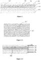
- the irregular-shaped display screen as shown in Figure 1 , comprises a substrate 101 and an encapsulation layer 104, wherein the substrate 101 and the encapsulation layer 104 encapsulate a confined space, the substrate 101 is divided into an irregular-shaped display region 105 and a non-display region 107, the substrate 101 has a TFT driving layer 102 and a plurality of pixel defining layers 103 stacked in sequence thereon, the pixel defining layers 103 form a continuous network structure, the pixel defining layer 103 upon the irregular-shaped display region 105 has an open structure, the pixel defining layer 103 upon the non-display region 107 has a non-open state, the pixel defining layer 103 upon the irregular-shaped display region 105 has several rows and/or several columns of pixel display units 106 arranged therein, the pixel display
- the present invention also provides a vapor deposition mask for manufacturing the irregular-shaped display screen, comprising a plurality of mask strips 123 arranged in parallel, a mask frame 121 and a mask shield 120 arranged in sequence outside the mask strips 123, the mask strips 123 comprises a plurality of open window zones 124, wherein the open window zone 124 is provided with a full-etching open area 126 and a semi-etching open area 125, the full-etching open area 126 has a shape that fits a pixel arrangement structure of the irregular-shaped display region 105, the semi-etching open area 125 is for alleviating the stress endured by the mask strip and thus preventing the open pore of the full-etching open area 126 from deforming.
- the shape of the full-etching open area 126 is adjusted in a corresponding way, wherein the vapor deposition mask of Figures 8-10 is suitable for manufacturing an irregular-shaped display screen of area display.
- the manufacturing method of the irregular-shaped display screen comprises the following steps: providing a TFT driving layer 102 upon a substrate 101; coating an organic photoresist layer upon the TFT driving layer 102; exposing and developing the organic photoresist layer within an irregular-shaped display region 105, so as to form a pixel defining layer 103 having an open structure, wherein the open-structured pixel defining layer 103 has an arrangement structure that corresponds to a pixel arrangement structure within the irregular-shaped display region 105; and depositing pixel display units 106 within the open-structured pixel defining layer 103 by using the vapor deposition mask.
- the full-etching open area 126 of the vapor deposition mask has a shape that fits the pixel arrangement structure of the irregular-shaped display region 105.
- the irregular-shaped display screen of this embodiment comprises a substrate 101 and an encapsulation layer 104, wherein the substrate 101 and the encapsulation layer 104 encapsulate a confined space, the substrate 101 is divided into an irregular-shaped display region 105 and a non-display region 107, the substrate 101 has a TFT driving layer 102 and a plurality of pixel defining layers 103 stacked in sequence thereon, the pixel defining layers 103 form a continuous network structure, the pixel defining layer 103 upon the irregular-shaped display region 105 has an open structure, the pixel defining layer 103 upon the non-display region 107 has a non-open state, the irregular-shaped display region 105 is a single-point display region, the pixel defining layers 103 has one single pixel display unit 106 arranged therein. According to actual requirements, multiple single-point display regions may be arranged on the same screen, wherein each open-structured pixel defining layer 103 has one
- the manufacturing method of the irregular-shaped display screen of single-point display in this embodiment comprises the following steps: providing a TFT driving layer 102 upon a substrate 101; coating an organic photoresist layer upon the TFT driving layer 102; exposing and developing the organic photoresist layer within a single-point irregular-shaped display region, so as to form a pixel defining layer 103 having an open structure, while the photoresist layer within a non-display region 107 is not exposed, so that a non-open-structured pixel defining layer is formed, wherein the open-structured pixel defining layer has an arrangement structure that corresponds to a pixel arrangement structure within the single-point irregular-shaped display region; and depositing pixel display units 106 within the open-structured pixel defining layer 103 by using the vapor deposition mask.
- the full-etching open area 126 of the vapor deposition mask has a shape that fits the pixel arrangement structure of the single-point irregular-shaped display region.
- the irregular-shaped display screen of this embodiment has the same screen structure as Embodiment 1, except that the irregular-shaped display region 105 is a horizontal straight line or a vertical straight line.
- the pixel arrangement structure within the irregular-shaped display region 105 is shown in Figure 6-1 and Figure 6-2 , wherein the pixel display units 106 are arranged in a horizontal direction or a vertical direction within the display region.
- the manufacturing method of the irregular-shaped display screen of straight line display in this embodiment comprises the following steps: providing a TFT driving layer 102 upon a substrate 101; coating an organic photoresist layer upon the TFT driving layer 102; exposing and developing the organic photoresist layer within a straight line irregular-shaped display region, so as to form a pixel defining layer 103 having an open structure, while the photoresist layer within a non-display region 107 is not exposed, so that a non-open-structured pixel defining layer is formed, wherein the open-structured pixel defining layer has an arrangement structure that corresponds to a pixel arrangement structure within the straight line irregular-shaped display region; and depositing pixel display units 106 within the open-structured pixel defining layer 103 by using the vapor deposition mask.
- the full-etching open area 126 of the vapor deposition mask has a shape that fits the pixel arrangement structure of the straight line irregular-shaped display region.
- the irregular-shaped display screen of this embodiment has the same screen structure as Embodiment 1, except that the irregular-shaped display region 105 is an oblique line display region.
- the oblique line may form an acute angle or an obtuse angle with the horizontal plane.
- oblique lines with an acute angle and an obtuse angle such as 30° and 150°, 45° and 135°, 60° and 120°
- this embodiment only illustrate the situations of acute angles, and the arrangements of the oblique line display regions with corresponding obtuse angles can be obtained by mirroring the situations illustrated in this embodiment.
- the oblique line display region of this embodiment forms an intersection angle of ⁇ with respect to the horizontal plane
- the oblique line display region is provided with several rows and/or several columns of pixel display units 106, wherein neighboring rows and/or neighboring columns of the pixel display units 106 are arranged in parallel, so as to cause a line connecting two pixel display units 106 farthest apart within the display region to form an intersection angle of ⁇ with respect to the horizontal plane.
- each pixel display unit group includes 3 pixel display units arranged side-by-side in a horizontal direction, pixel display units at two ends of each pixel display unit group are respectively aligned with a single pixel display unit in a neighboring pixel display unit group; an outermost row at one end of the display region is provided with one single pixel display unit; a line connecting two pixel display units farthest apart within the display region forms an angle of 30° with the horizontal plane.
- the first row and the second row of pixel display unit groups respectively have three pixel display units arranged side-by-side in a horizontal direction, the rightmost pixel display unit in the first row is positioned in the same column with the leftmost pixel display unit in the second row; the third row has one single pixel display unit which is positioned in the same column with the rightmost pixel display unit in the second row; and so on. If the length of the oblique line display region is longer than what is shown in this figure, the pixel arrangement structure of the first row and the second row can be repeated.
- the display region is provided with multiple rows of pixel display unit groups, wherein each pixel display unit group includes 2 pixel display units arranged side-by-side in a horizontal direction, the 2 pixel display units in each pixel display unit group are respectively aligned with a pixel display unit in a neighboring pixel display unit group; a line connecting two pixel display units farthest apart within the display region forms an angle of 45° with the horizontal plane.
- the first row, the second row and the third row of pixel display unit groups respectively have two pixel display units arranged side-by-side in a horizontal direction, the rightmost pixel display unit in the first row is positioned in the same column with the leftmost pixel display unit in the second row, the rightmost pixel display unit in the second row is positioned in the same column with the leftmost pixel display unit in the third row; and so on. If the length of the oblique line display region is longer than what is shown in this figure, the pixel arrangement structure of the first row and the second row can be repeated.
- the display region is provided with multiple columns of pixel display unit groups, wherein each pixel display unit group includes 3 pixel display units arranged side-by-side in a vertical direction, pixel display units at two ends of each pixel display unit group are respectively aligned with a single pixel display unit in a neighboring pixel display unit group; an outermost column at two ends of the display region is provided with one single pixel display unit; a line connecting two pixel display units farthest apart within the display region forms an angle of 60° with the horizontal plane.
- the second column and the third column of pixel display unit groups respectively have two pixel display units arranged side-by-side in a vertical direction, the uppermost pixel display unit in the first column is positioned in the same row with the lowermost pixel display unit in the second column, the first column has one single pixel display unit which is positioned in the same row with the lowermost pixel display unit in the second column, the fourth column has one single pixel display unit which is positioned in the same row with the uppermost pixel display unit in the third column; and so on. If the length of the oblique line display region is longer than what is shown in this figure, the pixel arrangement structure of the second column and the third column can be repeated.
- the display region has a length of L
- one pixel display unit has a length of L0
- S 4 3 ⁇ 90 ⁇ ⁇ 90 ⁇ 60 + 2 ⁇ ⁇ ⁇ 60 90 ⁇ 60 ⁇ L 2 1 2 ⁇ L 0 .
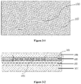
- the irregular-shaped display screen of this embodiment has the same screen structure as Embodiment 1, except that the irregular-shaped display region 105 is a curved line display region as shown in Figure 3-1 and Figure 3-2 .
- the curved line display region is decomposed into small oblique line segments having different angles, wherein each oblique line segment is provided with 2 to 3 pixel display units 106; several rows and/or several columns of pixel display units are provided within the oblique line segment, wherein neighboring rows and/or neighboring columns of the pixel display units are arranged in parallel, so as to cause a line connecting two pixel display units farthest apart within the oblique line segment to form an angle of ⁇ with respect to the horizontal plane.
- the pixel display units 106 are arranged in accordance with the manner described in Embodiment 3.
- the manufacturing method of the irregular-shaped display screen of curved line display in this embodiment comprises the following steps: providing a TFT driving layer 102 upon a substrate 101; coating an organic photoresist layer upon the TFT driving layer 102; exposing and developing the organic photoresist layer within a curved line irregular-shaped display region, so as to form a pixel defining layer 103 having an open structure, while the photoresist layer within a non-display region 107 is not exposed, so that a non-open-structured pixel defining layer is formed, wherein the open-structured pixel defining layer has an arrangement structure that corresponds to a pixel arrangement structure within the curved line irregular-shaped display region; and depositing pixel display units 106 within the open-structured pixel defining layer by using the vapor deposition mask.
- the full-etching open area 126 of the vapor deposition mask has a shape that fits the pixel arrangement structure of the curved line irregular-shaped display region.
- the irregular-shaped display screen of this embodiment has the same screen structure as Embodiment 1, except that the irregular-shaped display region 105 is an area display region as shown in Figure 5-1 and Figure 5-2 .
- the area display region is decomposed into oblique line display regions having different angles and a border line display region.
- Each of the oblique line display regions is provided with several rows and/or several columns of pixel display units 106, wherein neighboring rows and/or neighboring columns of the pixel display units 106 are arranged in parallel, so as to cause a line connecting two pixel display units farthest apart within the oblique line display region to form an angle, with the horizontal plane, equal to the intersection angle between the oblique line and the horizontal plane.
- the pixel display units 106 are arranged in accordance with the manner described in Embodiment 3.
- the border line display region is decomposed into small oblique line segment display regions having different angles, wherein each oblique line segment display region is provided with 2 to 3 pixel display units 106; several rows and/or several columns of pixel display units 106 are provided within the oblique line segment display region, wherein neighboring rows and/or neighboring columns of the pixel display units 106 are arranged in parallel, so as to cause a line connecting two pixel display units 106 farthest apart within the oblique line segment display region to form an angle, with the horizontal plane, equal to the intersection angle between the oblique line segment and the horizontal plane.
- the pixel display units 106 are arranged in accordance with the manner described in Embodiment 3.
- the manufacturing method of the irregular-shaped display screen of area display in this embodiment comprises the following steps: providing a TFT driving layer 102 upon a substrate 101; coating an organic photoresist layer upon the TFT driving layer 102; exposing and developing the organic photoresist layer within an area irregular-shaped display region, so as to form a pixel defining layer 103 having an open structure, while the photoresist layer within a non-display region 107 is not exposed, so that a non-open-structured pixel defining layer is formed, wherein the open-structured pixel defining layer has an arrangement structure that corresponds to a pixel arrangement structure within the area irregular-shaped display region; and depositing pixel display units 106 within the open-structured pixel defining layer 103 by using the vapor deposition mask.
- the full-etching open area 126 of the vapor deposition mask has a shape that fits the pixel arrangement structure of the area irregular-shaped display region.
Landscapes
- Chemical & Material Sciences (AREA)
- Engineering & Computer Science (AREA)
- Microelectronics & Electronic Packaging (AREA)
- Metallurgy (AREA)
- Materials Engineering (AREA)
- Mechanical Engineering (AREA)
- Chemical Kinetics & Catalysis (AREA)
- Organic Chemistry (AREA)
- Physics & Mathematics (AREA)
- Geometry (AREA)
- Manufacturing & Machinery (AREA)
- Electroluminescent Light Sources (AREA)
- Devices For Indicating Variable Information By Combining Individual Elements (AREA)
- Physical Vapour Deposition (AREA)
Abstract
Description
- The present invention relates to the field of organic electroluminescence display, and in particular relates to a pixel arrangement structure used for irregular-shaped display, a vapor deposition mask for manufacturing the pixel arrangement structure of irregular-shaped display, and an irregular-shaped display screen.
- Organic Light-Emitting Display (OLED) devices have the advantages such as active light-emitting, light-and-thin, a wide viewing angle, fast response speed, energy-saving, a large range of temperature tolerance, ability to realize flexible display as well as transparent display, and thus is regarded as the next-generation most potential new flat panel display technology.
- With people's various demands increase in the field of display, irregular-shaped display devices are becoming more and more popular. Because the pixel arrangement structure in prior arts is a lattice arrangement, an edge of an irregular-shaped display region would have a stepwise arrangement of pixels that does not have a regular pattern and would usually exceed the display region to a relatively large extent, this causes waste of materials for other layers, and meanwhile it is difficult to narrow the rim portion of the irregular-shaped display screen, which causes confusion at the interface between a display region and a non-display region.
- The present invention provides a pixel arrangement structure for an irregular-shaped display region, wherein, by means of arranging the pixel display units within the irregular-shaped display region in such a way that the neighboring rows and/or neighboring columns of the pixel display units are parallel rows or columns, a confusion phenomenon at the interface between a display region and a non-display region on an edge of the display region is eliminated.
- The present invention also provides a vapor deposition mask for manufacturing the pixel arrangement structure of irregular-shaped display, and an irregular-shaped display screen.
- In order to solve the above-mentioned technical problem, the present invention is realized by the following technical schemes:
A pixel arrangement structure is used for irregular-shaped display of an irregular-shaped display screen, the pixel arrangement structure is provided with several rows and/or several columns of pixel display units, wherein neighboring rows and/or neighboring columns of the pixel display units are arranged in parallel within an irregular-shaped display region. - The irregular-shaped display is single-point display, line display, area display or a combination thereof.
- The single-point display is adapted for being used by a screen having a single-point display region, and one single pixel display unit is provided within the single-point display region.
- The line display is adapted for being used by a screen having a single-line display region, and the single-line display region is a straight line display region, an oblique line display region and/or a curved line display region.
- The oblique line display region forms an intersection angle of θ with respect to the horizontal plane, the oblique line display region is provided with several rows and/or several columns of pixel display units, wherein neighboring rows and/or neighboring columns of the pixel display units are arranged in parallel, so as to cause a line connecting two pixel display units farthest apart within the oblique line display region to form an intersection angle of θ with respect to the horizontal plane. In accordance with variation of the angle θ, the pixel arrangement structure in the straight line display region or the oblique line display region is as follows:
when θ = 90° or 0°, the pixel display units are arranged in a vertical direction or a horizontal direction within the display region;
when θ = 30° or 150°, the display region is provided with multiple rows of pixel display unit groups, wherein each pixel display unit group includes 3 pixel display units arranged side-by-side in a horizontal direction, pixel display units at two ends of each pixel display unit group are respectively aligned with a single pixel display unit in a neighboring pixel display unit group; an outermost row at one end of the display region is provided with one single pixel display unit; a line connecting two pixel display units farthest apart within the display region forms an angle of 30° or 150° with the horizontal plane;
when θ = 45° or 135°, the display region is provided with multiple rows of pixel display unit groups, wherein each pixel display unit group includes 2 pixel display units arranged side-by-side in a horizontal direction, the 2 pixel display units in each pixel display unit group are respectively aligned with a pixel display unit in a neighboring pixel display unit group; a line connecting two pixel display units farthest apart within the display region forms an angle of 45° or 135° with the horizontal plane;
when θ = 60° or 120°, the display region is provided with multiple columns of pixel display unit groups, wherein each pixel display unit group includes 3 pixel display units arranged side-by-side in a vertical direction, pixel display units at two ends of each pixel display unit group are respectively aligned with a single pixel display unit in a neighboring pixel display unit group; an outermost column at two ends of the display region is provided with one single pixel display unit; a line connecting two pixel display units farthest apart within the display region forms an angle of 60° or 120° with the horizontal plane;
when 45°<θ<60°, pixel display units having an arrangement like that of θ = 60° account for (60-θ)/(60-45) of the oblique line, and pixel display units having an arrangement like that of θ = 45° account for (θ-45)/(60-45) of the oblique line; the display region has a length of L, one pixel display unit has a length of L0, and the display region is provided with S1 pixel display units arranged in a horizontal direction and S2 pixel display units arranged in a vertical direction:


- When the display region is a curved line display region, the curved line display region is decomposed into small oblique line segments having different angles, wherein each oblique line segment is provided with 2 to 3 pixel display units,
several rows and/or several columns of pixel display units are provided within the oblique line segment, wherein neighboring rows and/or neighboring columns of the pixel display units are arranged in parallel, so as to cause a line connecting two pixel display units farthest apart within the oblique line segment to form an angle of θ with respect to the horizontal plane. - The area display is adapted for being used by a screen having an area display region, and when pixels are arranged, the area display region is decomposed into oblique line display regions having different angles and a border line display region,
each of the oblique line display regions is provided with several rows and/or several columns of pixel display units, wherein neighboring rows and/or neighboring columns of the pixel display units are arranged in parallel, so as to cause a line connecting two pixel display units farthest apart within the oblique line display region to form an angle, with the horizontal plane, equal to the intersection angle between the oblique line and the horizontal plane;
the border line display region is decomposed into small oblique line segment display regions having different angles, wherein each oblique line segment display region is provided with 2 to 3 pixel display units; several rows and/or several columns of pixel display units are provided within the oblique line segment display region, wherein neighboring rows and/or neighboring columns of the pixel display units are arranged in parallel, so as to cause a line connecting two pixel display units farthest apart within the oblique line segment display region to form an angle, with the horizontal plane, equal to the intersection angle between the oblique line segment and the horizontal plane. - The pixel display units comprise one or more selected from a red light sub-pixel, a green light sub-pixel, a blue light sub-pixel.
- An irregular-shaped display screen, comprising a substrate and a TFT driving layer provided upon the substrate, the substrate is divided into an irregular-shaped display region and a non-display region, a plurality of pixel defining layers are provided upon the TFT driving layer, the pixel defining layers form a continuous network structure, wherein, the pixel defining layer upon the irregular-shaped display region has an open structure, the pixel defining layer upon the non-display region has a non-open state, the irregular-shaped display region is provided with the above-mentioned pixel arrangement structure.
- A vapor deposition mask for manufacturing an irregular-shaped display screen, comprising a plurality of mask strips arranged in parallel, a mask frame and a mask shield arranged in sequence outside the mask strips, wherein the mask strips comprises a plurality of open window zones, wherein, the open window zone is provided with a full-etching open area and a semi-etching open area, and the full-etching open area has a shape that fits a pixel arrangement structure of the irregular-shaped display region.
- A manufacturing method of the irregular-shaped display screen, comprising the following steps: providing a TFT driving layer upon a substrate; coating an organic photoresist layer upon the TFT driving layer; exposing and developing the organic photoresist layer within an irregular-shaped display region, so as to form a pixel defining layer having an open structure, wherein the open-structured pixel defining layer has an arrangement structure that corresponds to a pixel arrangement structure within the irregular-shaped display region; and depositing pixel display units within the open-structured pixel defining layer by using the above-mentioned vapor deposition mask.
- The full-etching open area of the vapor deposition mask has a shape that fits the pixel arrangement structure of the irregular-shaped display region.
- As compared to the prior art, the above-mentioned technical schemes of the present invention have the following advantages:
- (1) In the pixel arrangement structure used for irregular-shaped display provided by the present invention, several rows and/or several columns of pixel display units are provided within an irregular-shaped display region, wherein neighboring rows and/or neighboring columns of the pixel display units are arranged in parallel within the irregular-shaped display region. Different pixel display unit arrangement structures are used in accordance with different irregular-shaped display regions, so that the irregular-shaped display region can be controlled most precisely, especially for the edge of the irregular-shaped display region, thereby making the edge of the irregular-shaped display region smooth and clear. In the meantime, it is beneficial for the design of subsequent film layers and would not cause waste of materials.
- (2) When the irregular-shaped display region is a single-point display region, a line display region, an area display region or a combination thereof, the pixel display unit arrangement structures are respectively as follows:
- ① when the irregular-shaped display region is a single-point display region: the pixel defining layer upon the single-point display region has an open structure, the pixel defining layer upon the non-display region has a non-open state, and the open-structured pixel defining layer has one single pixel display unit arranged therein.
- ② when the irregular-shaped display region is a straight line or oblique line display region: the pixel defining layer upon the line display region has an open structure, the pixel defining layer upon the non-display region has a non-open state, and the open-structured pixel defining layer has several rows and/or several columns of pixel display units arranged therein, wherein neighboring rows and/or neighboring columns of the pixel display units are arranged in parallel, so as to cause a line connecting two pixel display units farthest apart within the oblique line display region to form an intersection angle of θ with respect to the horizontal plane. With different angles θ, such as 30°, 45° and 60°, the arrangements of pixel display units are also different. Because the arrangement of pixel display units is adjusted according to the variation of the angle of the oblique line, the problem of confused interface on an edge of the irregular-shaped display region can be prevented to the greatest extent possible.
- ③ when the irregular-shaped display region is a curved line display region: the curved line display region is decomposed into small oblique line segments having different angles, wherein each oblique line segment is provided with 2 to 3 pixel display units; according to different angles of each oblique line segment, the pixel display units are arranged in accordance with the rule of the pixel arrangement structure for the oblique line segments.
- ④ when the irregular-shaped display region is an area display region: the area display region is decomposed into oblique line display regions having different angles and a border line display region; according to different angles of each oblique line display region, the pixel display units are arranged in accordance with the rule of the pixel arrangement structure for the oblique line display regions; and the border line display region is further decomposed into small oblique line segment display regions having different angles, wherein each oblique line segment display region is provided with 2 to 3 pixel display units; according to different angles of each oblique line segment, the pixel display units are arranged in accordance with the rule of the pixel arrangement structure for the oblique line segments.
- (3) The pixel defining layers of the irregular-shaped display screen of the present invention vary according to different distribution regions, wherein the pixel defining layer upon the irregular-shaped display region has an open structure, and the pixel defining layer upon the non-display region has a non-open state. In this way, positioning of the display region can be realized, and meanwhile the materials can be saved.
- In order to make the content of the present invention easier to be understood clearly, hereinafter, the present invention is further described in detail with reference to the accompanying drawings, wherein,
-
Figure 1 is a structural schematic diagram of a pixel arrangement structure for an irregular-shaped display region according to the present invention; -
Figure 2-1 and Figure 2-2 are structural schematic diagrams of a pixel arrangement structure for a single-point irregular-shaped display region; -
Figure 3-1 and Figure 3-2 are structural schematic diagrams of a pixel arrangement structure for a line irregular-shaped display region; -
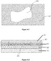
Figure 4-1 and Figure 4-2 are structural schematic diagrams of a pixel arrangement structure for an area irregular-shaped display region; -
Figure 5-1 and Figure 5-2 are schematic diagrams of another embodiment of a pixel arrangement structure for an area irregular-shaped display region; -
Figure 6-1 to Figure 6-5 are schematic diagrams of pixel display unit arrangement structures; -
Figure 7 is a schematic diagram of a pixel display unit; -
Figure 8 is a schematic diagram of a vapor deposition mask; -
Figure 9 is a detailed view of a mask strip; -
Figure 10 is a structural schematic diagram of an open window zone. - The reference numerals in the Drawings represent:
- 101-substrate, 102-TFT driving layer, 103-pixel defining layer, 104-encapsulation layer,
- 105-irregular-shaped display region, 106-pixel display unit, 107-non-display region,
- 120-mask shield, 121-mask frame, 123-mask strip, 124-open window zone,
- 125-semi-etching open area, 126-full-etching open area.
- In order to make the objective, technical scheme and advantages of the present invention clearer, detailed description of embodiments of the present invention is further given below, with reference to the accompanying drawings.
- The present invention can be implemented in many different forms and should not be interpreted to be limited to the embodiments described herein. On the contrary, by providing these embodiments, the present disclosure is made complete and thorough, and the inventive concept of the present invention is sufficiently conveyed to those skilled in the art, wherein the present invention is only defined by the Claims. In the accompanying drawings, for the sake of clarity, dimensions and relative sizes of layers and areas might be exaggerated. It should be understood that, when one element such as a layer, an area or a substrate plate is described as "formed on" or "configured on" another element, this one element may be configured directly upon that another element, or there may exist intermediate element(s). On the contrary, when one element is described as "directly formed upon" or "directly configured upon" another element, there exist no intermediate element.
- As shown in
Figure 1 to Figure 7 , the present invention provides a pixel arrangement structure, used for irregular-shaped display, and an irregular-shaped display screen having this pixel arrangement structure. The irregular-shaped display screen, as shown inFigure 1 , comprises asubstrate 101 and anencapsulation layer 104, wherein thesubstrate 101 and theencapsulation layer 104 encapsulate a confined space, thesubstrate 101 is divided into an irregular-shapeddisplay region 105 and anon-display region 107, thesubstrate 101 has aTFT driving layer 102 and a plurality ofpixel defining layers 103 stacked in sequence thereon, thepixel defining layers 103 form a continuous network structure, thepixel defining layer 103 upon the irregular-shapeddisplay region 105 has an open structure, thepixel defining layer 103 upon thenon-display region 107 has a non-open state, thepixel defining layer 103 upon the irregular-shapeddisplay region 105 has several rows and/or several columns ofpixel display units 106 arranged therein, thepixel display units 106 within the irregular-shapeddisplay region 106 are arranged in such a way that the neighboring rows and/or neighboring columns of thepixel display units 106 are parallel rows or columns, thepixel display units 106 include one or more of a red light subpixel, a green light subpixel and a blue light subpixel. The irregular-shapeddisplay region 105 is a single-point display region, a line display region, an area display region or a combination thereof, - As shown in
Figure 8 to Figure 10 , the present invention also provides a vapor deposition mask for manufacturing the irregular-shaped display screen, comprising a plurality of mask strips 123 arranged in parallel, amask frame 121 and amask shield 120 arranged in sequence outside the mask strips 123, the mask strips 123 comprises a plurality ofopen window zones 124, wherein theopen window zone 124 is provided with a full-etchingopen area 126 and a semi-etchingopen area 125, the full-etchingopen area 126 has a shape that fits a pixel arrangement structure of the irregular-shapeddisplay region 105, the semi-etchingopen area 125 is for alleviating the stress endured by the mask strip and thus preventing the open pore of the full-etchingopen area 126 from deforming. According to the shape of the above-mentioned irregular-shapeddisplay region 105, the shape of the full-etchingopen area 126 is adjusted in a corresponding way, wherein the vapor deposition mask ofFigures 8-10 is suitable for manufacturing an irregular-shaped display screen of area display. - The manufacturing method of the irregular-shaped display screen comprises the following steps: providing a
TFT driving layer 102 upon asubstrate 101; coating an organic photoresist layer upon theTFT driving layer 102; exposing and developing the organic photoresist layer within an irregular-shapeddisplay region 105, so as to form apixel defining layer 103 having an open structure, wherein the open-structuredpixel defining layer 103 has an arrangement structure that corresponds to a pixel arrangement structure within the irregular-shapeddisplay region 105; and depositingpixel display units 106 within the open-structuredpixel defining layer 103 by using the vapor deposition mask. The full-etchingopen area 126 of the vapor deposition mask has a shape that fits the pixel arrangement structure of the irregular-shapeddisplay region 105. - In accordance with different irregular-shaped
display regions 105, the following embodiments are illustrated: - The irregular-shaped display screen of this embodiment, as shown in
Figure 2-1 and Figure 2-2 , comprises asubstrate 101 and anencapsulation layer 104, wherein thesubstrate 101 and theencapsulation layer 104 encapsulate a confined space, thesubstrate 101 is divided into an irregular-shapeddisplay region 105 and anon-display region 107, thesubstrate 101 has aTFT driving layer 102 and a plurality ofpixel defining layers 103 stacked in sequence thereon, thepixel defining layers 103 form a continuous network structure, thepixel defining layer 103 upon the irregular-shapeddisplay region 105 has an open structure, thepixel defining layer 103 upon thenon-display region 107 has a non-open state, the irregular-shapeddisplay region 105 is a single-point display region, thepixel defining layers 103 has one singlepixel display unit 106 arranged therein. According to actual requirements, multiple single-point display regions may be arranged on the same screen, wherein each open-structuredpixel defining layer 103 has one singlepixel display unit 106 arranged therein. - The manufacturing method of the irregular-shaped display screen of single-point display in this embodiment comprises the following steps:
providing aTFT driving layer 102 upon asubstrate 101; coating an organic photoresist layer upon theTFT driving layer 102; exposing and developing the organic photoresist layer within a single-point irregular-shaped display region, so as to form apixel defining layer 103 having an open structure, while the photoresist layer within anon-display region 107 is not exposed, so that a non-open-structured pixel defining layer is formed, wherein the open-structured pixel defining layer has an arrangement structure that corresponds to a pixel arrangement structure within the single-point irregular-shaped display region; and depositingpixel display units 106 within the open-structuredpixel defining layer 103 by using the vapor deposition mask. The full-etchingopen area 126 of the vapor deposition mask has a shape that fits the pixel arrangement structure of the single-point irregular-shaped display region. - The irregular-shaped display screen of this embodiment has the same screen structure as Embodiment 1, except that the irregular-shaped
display region 105 is a horizontal straight line or a vertical straight line. The pixel arrangement structure within the irregular-shapeddisplay region 105 is shown inFigure 6-1 and Figure 6-2 , wherein thepixel display units 106 are arranged in a horizontal direction or a vertical direction within the display region. - The manufacturing method of the irregular-shaped display screen of straight line display in this embodiment comprises the following steps:
providing aTFT driving layer 102 upon asubstrate 101; coating an organic photoresist layer upon theTFT driving layer 102; exposing and developing the organic photoresist layer within a straight line irregular-shaped display region, so as to form apixel defining layer 103 having an open structure, while the photoresist layer within anon-display region 107 is not exposed, so that a non-open-structured pixel defining layer is formed, wherein the open-structured pixel defining layer has an arrangement structure that corresponds to a pixel arrangement structure within the straight line irregular-shaped display region; and depositingpixel display units 106 within the open-structuredpixel defining layer 103 by using the vapor deposition mask. The full-etchingopen area 126 of the vapor deposition mask has a shape that fits the pixel arrangement structure of the straight line irregular-shaped display region. - The irregular-shaped display screen of this embodiment has the same screen structure as Embodiment 1, except that the irregular-shaped
display region 105 is an oblique line display region. The oblique line may form an acute angle or an obtuse angle with the horizontal plane. Considering that oblique lines with an acute angle and an obtuse angle (such as 30° and 150°, 45° and 135°, 60° and 120°) are mirrored towards a vertical axis, this embodiment only illustrate the situations of acute angles, and the arrangements of the oblique line display regions with corresponding obtuse angles can be obtained by mirroring the situations illustrated in this embodiment. - The oblique line display region of this embodiment forms an intersection angle of θ with respect to the horizontal plane, the oblique line display region is provided with several rows and/or several columns of
pixel display units 106, wherein neighboring rows and/or neighboring columns of thepixel display units 106 are arranged in parallel, so as to cause a line connecting twopixel display units 106 farthest apart within the display region to form an intersection angle of θ with respect to the horizontal plane. In particular:
When θ = 30°, the display region is provided with multiple rows of pixel display unit groups, as shown inFigure 6-3 , each pixel display unit group includes 3 pixel display units arranged side-by-side in a horizontal direction, pixel display units at two ends of each pixel display unit group are respectively aligned with a single pixel display unit in a neighboring pixel display unit group; an outermost row at one end of the display region is provided with one single pixel display unit; a line connecting two pixel display units farthest apart within the display region forms an angle of 30° with the horizontal plane. Specifically, as viewed from a direction facing the drawing plane ofFigure 6-3 , from downside to upside in the display region, the first row and the second row of pixel display unit groups respectively have three pixel display units arranged side-by-side in a horizontal direction, the rightmost pixel display unit in the first row is positioned in the same column with the leftmost pixel display unit in the second row; the third row has one single pixel display unit which is positioned in the same column with the rightmost pixel display unit in the second row; and so on. If the length of the oblique line display region is longer than what is shown in this figure, the pixel arrangement structure of the first row and the second row can be repeated. - When θ = 45°, the display region is provided with multiple rows of pixel display unit groups, wherein each pixel display unit group includes 2 pixel display units arranged side-by-side in a horizontal direction, the 2 pixel display units in each pixel display unit group are respectively aligned with a pixel display unit in a neighboring pixel display unit group; a line connecting two pixel display units farthest apart within the display region forms an angle of 45° with the horizontal plane. Specifically, as viewed from a direction facing the drawing plane of
Figure 6-4 , from downside to upside in the display region, the first row, the second row and the third row of pixel display unit groups respectively have two pixel display units arranged side-by-side in a horizontal direction, the rightmost pixel display unit in the first row is positioned in the same column with the leftmost pixel display unit in the second row, the rightmost pixel display unit in the second row is positioned in the same column with the leftmost pixel display unit in the third row; and so on. If the length of the oblique line display region is longer than what is shown in this figure, the pixel arrangement structure of the first row and the second row can be repeated. - When θ = 60°, the display region is provided with multiple columns of pixel display unit groups, wherein each pixel display unit group includes 3 pixel display units arranged side-by-side in a vertical direction, pixel display units at two ends of each pixel display unit group are respectively aligned with a single pixel display unit in a neighboring pixel display unit group; an outermost column at two ends of the display region is provided with one single pixel display unit; a line connecting two pixel display units farthest apart within the display region forms an angle of 60° with the horizontal plane. Specifically, as viewed from a direction facing the drawing plane of
Figure 6-4 , from left to right in the display region, the second column and the third column of pixel display unit groups respectively have two pixel display units arranged side-by-side in a vertical direction, the uppermost pixel display unit in the first column is positioned in the same row with the lowermost pixel display unit in the second column, the first column has one single pixel display unit which is positioned in the same row with the lowermost pixel display unit in the second column, the fourth column has one single pixel display unit which is positioned in the same row with the uppermost pixel display unit in the third column; and so on. If the length of the oblique line display region is longer than what is shown in this figure, the pixel arrangement structure of the second column and the third column can be repeated. - When 45°<θ<60°, pixel display units having an arrangement like that of θ = 60° account for (60-θ)/(60-45) of the oblique line, and pixel display units having an arrangement like that of θ = 45° account for (θ-45)/(60-45) of the oblique line. Specifically, when θ = 50°, pixel display units having an arrangement like that of θ = 60° account for (60-50)/(60-45) = 10/15 = 2/3 of the oblique line, and pixel display units having an arrangement like that of θ = 45° account for (50-45)/(60-45) = 5/15 = 1/3 of the oblique line. That is to say, within this oblique line display region, 2/3 of the pixel arrangement structure is arranged in accordance with the rule of the 60° angle oblique line pixel arrangement, 1/3 of the pixel arrangement structure is arranged in accordance with the rule of the 45° angle oblique line pixel arrangement, and a line connecting two pixel display units farthest apart within this display region forms an intersection angle of 50° with the horizontal plane. The display region has a length of L, one pixel display unit has a length of L0, and the display region is provided with S1 pixel display units arranged in a horizontal direction and S2 pixel display units arranged in a vertical direction:


- When 60°<θ<90°, pixel display units having an arrangement like that of θ = 90° account for (90-θ)/(90-60) of the oblique line, and pixel display units having an arrangement like that of θ = 60° account for (θ-60)/(90-60) of the oblique line; the display region has a length of L, one pixel display unit has a length of L0, and the display region is provided with S3 pixel display units arranged in a horizontal direction and S4 pixel display units arranged in a vertical direction:


- The irregular-shaped display screen of this embodiment has the same screen structure as Embodiment 1, except that the irregular-shaped
display region 105 is a curved line display region as shown inFigure 3-1 and Figure 3-2 . the curved line display region is decomposed into small oblique line segments having different angles, wherein each oblique line segment is provided with 2 to 3pixel display units 106; several rows and/or several columns of pixel display units are provided within the oblique line segment, wherein neighboring rows and/or neighboring columns of the pixel display units are arranged in parallel, so as to cause a line connecting two pixel display units farthest apart within the oblique line segment to form an angle of θ with respect to the horizontal plane. According to different angles that each oblique line segment forms with the horizontal plane, thepixel display units 106 are arranged in accordance with the manner described in Embodiment 3. - The manufacturing method of the irregular-shaped display screen of curved line display in this embodiment comprises the following steps:
providing aTFT driving layer 102 upon asubstrate 101; coating an organic photoresist layer upon theTFT driving layer 102; exposing and developing the organic photoresist layer within a curved line irregular-shaped display region, so as to form apixel defining layer 103 having an open structure, while the photoresist layer within anon-display region 107 is not exposed, so that a non-open-structured pixel defining layer is formed, wherein the open-structured pixel defining layer has an arrangement structure that corresponds to a pixel arrangement structure within the curved line irregular-shaped display region; and depositingpixel display units 106 within the open-structured pixel defining layer by using the vapor deposition mask. The full-etchingopen area 126 of the vapor deposition mask has a shape that fits the pixel arrangement structure of the curved line irregular-shaped display region. - The irregular-shaped display screen of this embodiment has the same screen structure as Embodiment 1, except that the irregular-shaped
display region 105 is an area display region as shown inFigure 5-1 and Figure 5-2 . The area display region is decomposed into oblique line display regions having different angles and a border line display region. - Each of the oblique line display regions is provided with several rows and/or several columns of
pixel display units 106, wherein neighboring rows and/or neighboring columns of thepixel display units 106 are arranged in parallel, so as to cause a line connecting two pixel display units farthest apart within the oblique line display region to form an angle, with the horizontal plane, equal to the intersection angle between the oblique line and the horizontal plane. Specifically, according to different angles that each oblique line forms with the horizontal plane, thepixel display units 106 are arranged in accordance with the manner described in Embodiment 3. - The border line display region is decomposed into small oblique line segment display regions having different angles, wherein each oblique line segment display region is provided with 2 to 3
pixel display units 106; several rows and/or several columns ofpixel display units 106 are provided within the oblique line segment display region, wherein neighboring rows and/or neighboring columns of thepixel display units 106 are arranged in parallel, so as to cause a line connecting twopixel display units 106 farthest apart within the oblique line segment display region to form an angle, with the horizontal plane, equal to the intersection angle between the oblique line segment and the horizontal plane. Specifically, according to different angles that each oblique line segment forms with the horizontal plane, thepixel display units 106 are arranged in accordance with the manner described in Embodiment 3. - The manufacturing method of the irregular-shaped display screen of area display in this embodiment comprises the following steps:
providing aTFT driving layer 102 upon asubstrate 101; coating an organic photoresist layer upon theTFT driving layer 102; exposing and developing the organic photoresist layer within an area irregular-shaped display region, so as to form apixel defining layer 103 having an open structure, while the photoresist layer within anon-display region 107 is not exposed, so that a non-open-structured pixel defining layer is formed, wherein the open-structured pixel defining layer has an arrangement structure that corresponds to a pixel arrangement structure within the area irregular-shaped display region; and depositingpixel display units 106 within the open-structuredpixel defining layer 103 by using the vapor deposition mask. The full-etchingopen area 126 of the vapor deposition mask has a shape that fits the pixel arrangement structure of the area irregular-shaped display region. - Apparently, the aforementioned embodiments are merely examples illustrated for clearly describing the present invention, rather than limiting the implementation ways thereof. For a person skilled in the art, various changes and modifications in other different forms can be made on the basis of the aforementioned description. It is unnecessary and impossible to exhaustively list all the implementation ways herein. However, any obvious changes or modifications derived from the aforementioned description are intended to be embraced within the protection scope of the present invention.
Claims (13)
- A pixel arrangement structure, used for irregular-shaped display of an irregular-shaped display screen, characterized in that,
the pixel arrangement structure is provided with several rows and/or several columns of pixel display units, wherein neighboring rows and/or neighboring columns of the pixel display units are arranged in parallel within an irregular-shaped display region. - The pixel arrangement structure according to Claim 1, characterized in that, the irregular-shaped display is single-point display, line display, area display or a combination thereof.
- The pixel arrangement structure according to Claim 2, characterized in that, the single-point display is adapted for being used by a screen having a single-point display region, and one single pixel display unit is provided within the single-point display region.
- The pixel arrangement structure according to Claim 2, characterized in that, the line display is adapted for being used by a screen having a single-line display region, and the single-line display region is a straight line display region, an oblique line display region and/or a curved line display region.
- The pixel arrangement structure according to Claim 4, characterized in that, the oblique line display region forms an intersection angle of θ with respect to the horizontal plane, the oblique line display region is provided with several rows and/or several columns of pixel display units, wherein neighboring rows and/or neighboring columns of the pixel display units are arranged in parallel, so as to cause a line connecting two pixel display units farthest apart within the oblique line display region to form the intersection angle of θ with respect to the horizontal plane.
- The pixel arrangement structure according to Claim 5, characterized in that, in accordance with variation of the angle θ, the pixel arrangement structure in the straight line display region or the oblique line display region is as follows:when θ = 90° or 0°, the pixel display units are arranged in a vertical direction or a horizontal direction within the display region;when θ = 30° or 150°, the display region is provided with multiple rows of pixel display unit groups, wherein each pixel display unit group includes 3 pixel display units arranged side-by-side in a horizontal direction, pixel display units at two ends of each pixel display unit group are respectively aligned with a single pixel display unit in a neighboring pixel display unit group; an outermost row at one end of the display region is provided with one single pixel display unit; a line connecting two pixel display units farthest apart within the display region forms an angle of 30° or 150° with the horizontal plane;when θ = 45° or 135°, the display region is provided with multiple rows of pixel display unit groups, wherein each pixel display unit group includes 2 pixel display units arranged side-by-side in a horizontal direction, the 2 pixel display units in each pixel display unit group are respectively aligned with a pixel display unit in a neighboring pixel display unit group; a line connecting two pixel display units farthest apart within the display region forms an angle of 45° or 135° with the horizontal plane;when θ = 60° or 120°, the display region is provided with multiple columns of pixel display unit groups, wherein each pixel display unit group includes 3 pixel display units arranged side-by-side in a vertical direction, pixel display units at two ends of each pixel display unit group are respectively aligned with a single pixel display unit in a neighboring pixel display unit group; an outermost column at two ends of the display region is provided with one single pixel display unit; a line connecting two pixel display units farthest apart within the display region forms an angle of 60° or 120° with the horizontal plane;when 45°<θ<60°, pixel display units having an arrangement like that of θ = 60° account for (60-θ)/(60-45) of the oblique line, and pixel display units having an arrangement like that of θ = 45° account for (θ-45)/(60-45) of the oblique line; the display region has a length of L, one pixel display unit has a length of L0, and the display region is provided with S1 pixel display units arranged in a horizontal direction and S2 pixel display units arranged in a vertical direction:

 when 60°<θ<90°, pixel display units having an arrangement like that of θ = 90° account for (90-θ)/(90-60) of the oblique line, and pixel display units having an arrangement like that of θ = 60° account for (θ-60)/(90-60) of the oblique line; the display region has a length of L, one pixel display unit has a length of L0, and the display region is provided with S3 pixel display units arranged in a horizontal direction and S4 pixel display units arranged in a vertical direction:

- The pixel arrangement structure according to Claim 5, characterized in that, when the display region is a curved line display region, the curved line display region is decomposed into small oblique line segments having different angles, wherein each oblique line segment is provided with 2 to 3 pixel display units,
several rows and/or several columns of pixel display units are provided within the oblique line segment, wherein neighboring rows and/or neighboring columns of the pixel display units are arranged in parallel, so as to cause a line connecting two pixel display units farthest apart within the oblique line segment to form an angle of θ with respect to the horizontal plane. - The pixel arrangement structure according to Claim 2, characterized in that, the area display is adapted for being used by a screen having an area display region, and when pixels are arranged, the area display region is decomposed into oblique line display regions having different angles and a border line display region,
each of the oblique line display regions is provided with several rows and/or several columns of pixel display units, wherein neighboring rows and/or neighboring columns of the pixel display units are arranged in parallel, so as to cause a line connecting two pixel display units farthest apart within the oblique line display region to form an angle, with the horizontal plane, equal to the intersection angle between the oblique line and the horizontal plane;
the border line display region is decomposed into small oblique line segment display regions having different angles, wherein each oblique line segment display region is provided with 2 to 3 pixel display units; several rows and/or several columns of pixel display units are provided within the oblique line segment display region, wherein neighboring rows and/or neighboring columns of the pixel display units are arranged in parallel, so as to cause a line connecting two pixel display units farthest apart within the oblique line segment display region to form an angle, with the horizontal plane, equal to the intersection angle between the oblique line segment and the horizontal plane. - The pixel arrangement structure according to any one of Claims 1-8, characterized in that, the pixel display units comprise one or more selected from a red light sub-pixel, a green light sub-pixel, a blue light sub-pixel.
- An irregular-shaped display screen, comprising a substrate and a TFT driving layer provided upon the substrate, the substrate is divided into an irregular-shaped display region and a non-display region, a plurality of pixel defining layers are provided upon the TFT driving layer, the pixel defining layers form a continuous network structure, characterized in that,
the pixel defining layer upon the irregular-shaped display region has an open structure, the pixel defining layer upon the non-display region has a non-open state, the irregular-shaped display region is provided with pixel display units arranged in accordance with the pixel arrangement structure according to any one of Claims 1-9. - A vapor deposition mask for manufacturing an irregular-shaped display screen, comprising a plurality of mask strips (123) arranged in parallel, a mask frame (121) and a mask shield (120) arranged in sequence outside the mask strips (123), wherein the mask strips (123) comprises a plurality of open window zones (124), characterized in that, the open window zone (124) is provided with a full-etching open area (126) and a semi-etching open area (125), and the full-etching open area (126) has a shape that fits a pixel arrangement structure of the irregular-shaped display region.
- A manufacturing method of the irregular-shaped display screen according to Claim 10, characterized in comprising the following steps:providing a TFT driving layer upon a substrate;coating an organic photoresist layer upon the TFT driving layer;exposing and developing the organic photoresist layer within an irregular-shaped display region, so as to form a pixel defining layer having an open structure, wherein the open-structured pixel defining layer has an arrangement structure that corresponds to a pixel arrangement structure within the irregular-shaped display region; anddepositing pixel display units within the open-structured pixel defining layer by using the vapor deposition mask according to Claim 11.
- The manufacturing method according to Claim 12, characterized in that, the full-etching open area (126) of the vapor deposition mask has a shape that fits the pixel arrangement structure of the irregular-shaped display region.
Applications Claiming Priority (2)
| Application Number | Priority Date | Filing Date | Title |
|---|---|---|---|
| CN201610076497.4A CN107039485A (en) | 2016-02-03 | 2016-02-03 | A kind of pixel arrangement structure, evaporation mask plate and special-shaped display screen body |
| PCT/CN2017/072400 WO2017133566A1 (en) | 2016-02-03 | 2017-01-24 | Pixel arrangement structure, vapor deposition mask and profiled display screen |
Publications (2)
| Publication Number | Publication Date |
|---|---|
| EP3385991A1 true EP3385991A1 (en) | 2018-10-10 |
| EP3385991A4 EP3385991A4 (en) | 2018-11-21 |
Family
ID=59499378
Family Applications (1)
| Application Number | Title | Priority Date | Filing Date |
|---|---|---|---|
| EP17746886.5A Withdrawn EP3385991A4 (en) | 2016-02-03 | 2017-01-24 | Pixel arrangement structure, vapor deposition mask and profiled display screen |
Country Status (7)
| Country | Link |
|---|---|
| US (1) | US11257881B2 (en) |
| EP (1) | EP3385991A4 (en) |
| JP (1) | JP2019504360A (en) |
| KR (1) | KR20180084860A (en) |
| CN (1) | CN107039485A (en) |
| TW (2) | TWI652812B (en) |
| WO (1) | WO2017133566A1 (en) |
Families Citing this family (1)
| Publication number | Priority date | Publication date | Assignee | Title |
|---|---|---|---|---|
| CN110969944B (en) * | 2019-12-06 | 2020-12-25 | 深圳市华星光电半导体显示技术有限公司 | Special-shaped display screen and display device |
Family Cites Families (24)
| Publication number | Priority date | Publication date | Assignee | Title |
|---|---|---|---|---|
| US6949883B2 (en) | 2001-12-06 | 2005-09-27 | Seiko Epson Corporation | Electro-optical device and an electronic apparatus |
| TWM247856U (en) * | 2003-10-30 | 2004-10-21 | Display Optronics Corp M | A display with a non-rectangle panel |
| TWI267058B (en) * | 2004-10-08 | 2006-11-21 | Ind Tech Res Inst | Non-rectangular display device |
| CN100371806C (en) | 2005-07-19 | 2008-02-27 | 友达光电股份有限公司 | Display device sealing area pattern and forming method thereof |
| CN102902116B (en) | 2008-05-11 | 2016-02-10 | Nlt科技股份有限公司 | The pel array of non-rectangle and there is the display device of this array |
| JP5747425B2 (en) * | 2008-05-11 | 2015-07-15 | Nltテクノロジー株式会社 | Non-rectangular pixel array and display device including the array |
| CN101877209A (en) * | 2009-04-28 | 2010-11-03 | 英华达(上海)电子有限公司 | Character display method, display device and computer system |
| JP5178804B2 (en) * | 2010-10-28 | 2013-04-10 | ルネサスエレクトロニクス株式会社 | Driving method of imaging apparatus |
| JP2012103335A (en) | 2010-11-08 | 2012-05-31 | Hitachi Displays Ltd | Display device |
| KR101820020B1 (en) | 2011-04-25 | 2018-01-19 | 삼성디스플레이 주식회사 | Mask frame assembly for thin film deposition |
| CN102899636B (en) | 2012-09-26 | 2015-12-09 | 中微半导体设备(上海)有限公司 | A kind of method of In-Situ Cleaning MOCVD reaction chamber |
| KR101936619B1 (en) * | 2012-10-31 | 2019-01-09 | 엘지디스플레이 주식회사 | Flexible organic electroluminescent device and method for fabricating the same |
| KR102002494B1 (en) | 2012-11-30 | 2019-07-23 | 삼성디스플레이 주식회사 | Mask frame assembly for thin film deposition |
| KR102007831B1 (en) * | 2012-12-14 | 2019-08-06 | 엘지디스플레이 주식회사 | Narrow bezel type array substrate for liquid crystal display device |
| CN103123927B (en) | 2013-01-24 | 2015-05-06 | 昆山维信诺显示技术有限公司 | Pixel structure for OLED display screen and metal mask thereof |
| KR102055683B1 (en) | 2013-03-29 | 2019-12-16 | 삼성디스플레이 주식회사 | Organic light emitting display apparatus |
| CN103236398B (en) * | 2013-04-19 | 2015-09-09 | 深圳市华星光电技术有限公司 | The manufacture method of reticle mask plate and the reticle mask plate with the method making |
| KR102126435B1 (en) * | 2014-02-11 | 2020-06-25 | 삼성디스플레이 주식회사 | Display device |
| CN203799598U (en) * | 2014-03-31 | 2014-08-27 | 成卓 | LED display panel module and splicing structure thereof |
| KR102172980B1 (en) | 2014-04-07 | 2020-11-02 | 삼성전자주식회사 | Tiled display system and method for processing images thereof |
| KR102030830B1 (en) | 2014-07-18 | 2019-10-10 | 삼성전자주식회사 | Curved multiview image display apparatus and control method thereof |
| CN204424258U (en) * | 2014-12-31 | 2015-06-24 | 北京维信诺科技有限公司 | A kind of high-resolution pixel arrangement structure |
| CN204803392U (en) * | 2015-07-27 | 2015-11-25 | 昆山国显光电有限公司 | Accurate mask plate |
| CN105139797A (en) * | 2015-10-15 | 2015-12-09 | 京东方科技集团股份有限公司 | Special-shaped display panel and display device |
-
2016
- 2016-02-03 CN CN201610076497.4A patent/CN107039485A/en active Pending
-
2017
- 2017-01-24 JP JP2018535174A patent/JP2019504360A/en active Pending
- 2017-01-24 EP EP17746886.5A patent/EP3385991A4/en not_active Withdrawn
- 2017-01-24 WO PCT/CN2017/072400 patent/WO2017133566A1/en not_active Ceased
- 2017-01-24 KR KR1020187016194A patent/KR20180084860A/en not_active Ceased
- 2017-01-24 US US15/781,350 patent/US11257881B2/en active Active
- 2017-01-25 TW TW106103041A patent/TWI652812B/en active
- 2017-01-25 TW TW107136580A patent/TW201907561A/en unknown
Also Published As
| Publication number | Publication date |
|---|---|
| US20200273925A1 (en) | 2020-08-27 |
| WO2017133566A1 (en) | 2017-08-10 |
| US11257881B2 (en) | 2022-02-22 |
| CN107039485A (en) | 2017-08-11 |
| EP3385991A4 (en) | 2018-11-21 |
| KR20180084860A (en) | 2018-07-25 |
| TW201907561A (en) | 2019-02-16 |
| JP2019504360A (en) | 2019-02-14 |
| TWI652812B (en) | 2019-03-01 |
| TW201740554A (en) | 2017-11-16 |
Similar Documents
| Publication | Publication Date | Title |
|---|---|---|
| EP3270216B1 (en) | Pixel arrangement structure, display panel, and display device | |
| CN109994507B (en) | Pixel arrangement structure and related device | |
| US9997560B2 (en) | Display substrate, method for fabricating the same and display device | |
| CN105807508B (en) | Display panel and display device | |
| WO2019041910A1 (en) | Display panel and display device | |
| EP3203519B1 (en) | Array substrate, method of manufacturing the array substrate using a mask plate and display device | |
| EP3211478B1 (en) | Display panel and manufacturing method therefor | |
| US20150061978A1 (en) | Pixel arrangement of color display apparatus | |
| WO2020082540A1 (en) | Flexible oled panel and manufacturing method therefor | |
| US9831431B2 (en) | OLED curved-surface display panel and manufacturing method thereof, and display device | |
| CN105527746B (en) | Display master blank and preparation method thereof, display device | |
| WO2018188318A1 (en) | Colour film substrate and manufacturing method therefor, and relevant apparatus | |
| CN105629596A (en) | Display panel | |
| US9620537B2 (en) | Display substrate and fabricating method thereof, mask plate, and mask plate group | |
| US11950477B2 (en) | OLED display panel and OLED display device | |
| EP2618209B1 (en) | Active matrix substrate and electronic device comprising the same | |
| CN104808381A (en) | Display panel and display device | |
| CN104375310B (en) | Hook face display panel and hook face display device | |
| CN106094334A (en) | Display floater and display device | |
| CN107193161A (en) | Array base palte and display panel | |
| CN108227273B (en) | Display panel, color filter substrate and manufacturing method of color filter substrate | |
| US20210193770A1 (en) | Display substrate, display panel, display device and method for manufacturing display substrate | |
| CN112201681B (en) | Pixel arrangement structure, electroluminescent display panel, display device and mask plate | |
| US20200081301A1 (en) | Array substrate and display panel | |
| US11257881B2 (en) | Pixel arrangement structure, vapor deposition mask and irregular-shaped display screen |
Legal Events
| Date | Code | Title | Description |
|---|---|---|---|
| PUAI | Public reference made under article 153(3) epc to a published international application that has entered the european phase |
Free format text: ORIGINAL CODE: 0009012 |
|
| 17P | Request for examination filed |
Effective date: 20180702 |
|
| AK | Designated contracting states |
Kind code of ref document: A1 Designated state(s): AL AT BE BG CH CY CZ DE DK EE ES FI FR GB GR HR HU IE IS IT LI LT LU LV MC MK MT NL NO PL PT RO RS SE SI SK SM TR |
|
| AX | Request for extension of the european patent |
Extension state: BA ME |
|
| A4 | Supplementary search report drawn up and despatched |
Effective date: 20181024 |
|
| RIC1 | Information provided on ipc code assigned before grant |
Ipc: C23C 14/04 20060101ALN20181018BHEP Ipc: H01L 27/32 20060101AFI20181018BHEP Ipc: H01L 51/56 20060101ALI20181018BHEP |
|
| DAV | Request for validation of the european patent (deleted) | ||
| DAX | Request for extension of the european patent (deleted) | ||
| 17Q | First examination report despatched |
Effective date: 20190514 |
|
| STAA | Information on the status of an ep patent application or granted ep patent |
Free format text: STATUS: THE APPLICATION IS DEEMED TO BE WITHDRAWN |
|
| 18D | Application deemed to be withdrawn |
Effective date: 20200603 |