EP3385218A1 - Semiconductor device - Google Patents
Semiconductor device Download PDFInfo
- Publication number
- EP3385218A1 EP3385218A1 EP17164598.9A EP17164598A EP3385218A1 EP 3385218 A1 EP3385218 A1 EP 3385218A1 EP 17164598 A EP17164598 A EP 17164598A EP 3385218 A1 EP3385218 A1 EP 3385218A1
- Authority
- EP
- European Patent Office
- Prior art keywords
- semiconductor device
- substrate body
- environmental sensor
- gas
- volume
- Prior art date
- Legal status (The legal status is an assumption and is not a legal conclusion. Google has not performed a legal analysis and makes no representation as to the accuracy of the status listed.)
- Granted
Links
Images






Classifications
-
- B—PERFORMING OPERATIONS; TRANSPORTING
- B81—MICROSTRUCTURAL TECHNOLOGY
- B81B—MICROSTRUCTURAL DEVICES OR SYSTEMS, e.g. MICROMECHANICAL DEVICES
- B81B7/00—Microstructural systems ; Auxiliary parts of microstructural devices or systems
- B81B7/0032—Packages or encapsulation
- B81B7/0045—Packages or encapsulation for reducing stress inside of the package structure
- B81B7/0051—Packages or encapsulation for reducing stress inside of the package structure between the package lid and the substrate
-
- B—PERFORMING OPERATIONS; TRANSPORTING
- B81—MICROSTRUCTURAL TECHNOLOGY
- B81B—MICROSTRUCTURAL DEVICES OR SYSTEMS, e.g. MICROMECHANICAL DEVICES
- B81B7/00—Microstructural systems ; Auxiliary parts of microstructural devices or systems
- B81B7/0032—Packages or encapsulation
- B81B7/0045—Packages or encapsulation for reducing stress inside of the package structure
- B81B7/0048—Packages or encapsulation for reducing stress inside of the package structure between the MEMS die and the substrate
-
- B—PERFORMING OPERATIONS; TRANSPORTING
- B81—MICROSTRUCTURAL TECHNOLOGY
- B81B—MICROSTRUCTURAL DEVICES OR SYSTEMS, e.g. MICROMECHANICAL DEVICES
- B81B2201/00—Specific applications of microelectromechanical systems
- B81B2201/02—Sensors
- B81B2201/0264—Pressure sensors
-
- B—PERFORMING OPERATIONS; TRANSPORTING
- B81—MICROSTRUCTURAL TECHNOLOGY
- B81B—MICROSTRUCTURAL DEVICES OR SYSTEMS, e.g. MICROMECHANICAL DEVICES
- B81B2203/00—Basic microelectromechanical structures
- B81B2203/01—Suspended structures, i.e. structures allowing a movement
- B81B2203/0127—Diaphragms, i.e. structures separating two media that can control the passage from one medium to another; Membranes, i.e. diaphragms with filtering function
-
- B—PERFORMING OPERATIONS; TRANSPORTING
- B81—MICROSTRUCTURAL TECHNOLOGY
- B81B—MICROSTRUCTURAL DEVICES OR SYSTEMS, e.g. MICROMECHANICAL DEVICES
- B81B2203/00—Basic microelectromechanical structures
- B81B2203/03—Static structures
- B81B2203/0323—Grooves
- B81B2203/033—Trenches
-
- B—PERFORMING OPERATIONS; TRANSPORTING
- B81—MICROSTRUCTURAL TECHNOLOGY
- B81C—PROCESSES OR APPARATUS SPECIALLY ADAPTED FOR THE MANUFACTURE OR TREATMENT OF MICROSTRUCTURAL DEVICES OR SYSTEMS
- B81C2203/00—Forming microstructural systems
- B81C2203/03—Bonding two components
- B81C2203/032—Gluing
Definitions
- the present application relates to a semiconductor device.
- Semiconductor devices can comprise environmental sensors as, for example, pressure sensors.
- environmental sensors and especially pressure sensors are sensitive to stress.
- the semiconductor devices are calibrated before they are incorporated into a final product, e.g. a mobile phone, additional stress can be exerted on the semiconductor device within the final product. If the additional stress is transferred to the environmental sensor it is less accurate.
- Additional stress induced on a semiconductor device can be avoided, for example by the use of thick glue layers or thick ceramic substrates. However, in both cases the thickness and also the footprint of the semiconductor device are increased, which is not desirable for applications in mobile phones or other portable devices.
- the semiconductor device comprises a cap body.
- the cap body can be a wafer, a substrate or a bulk material and it can comprise silicon, glass or a semiconductor.
- the semiconductor device further comprises an environmental sensor.
- the environmental sensor can be a pressure sensor or, for example, a capacitive pressure sensor with a membrane.
- the cap body can be arranged on top of the environmental sensor. It is also possible that the semiconductor device comprises several environmental sensors.
- the semiconductor device further comprises a substrate body.
- the substrate body can be a wafer, a substrate or a bulk material and it can comprise silicon or glass.
- the substrate body can comprise an integrated circuit and a substrate. It is also possible that the substrate body comprises glass with a coefficient of thermal expansion which is similar to the coefficient of thermal expansion of the cap body.
- the cap body and the substrate body can be of the same material or they can comprise different materials.
- the environmental sensor is arranged on top of the substrate body, for example on top of the integrated circuit.
- the semiconductor device further comprises a first volume of gas.
- the environmental sensor and the first volume of gas are arranged between the substrate body and the cap body in a vertical direction which is perpendicular to the main plane of extension of the substrate body.
- the first volume of gas can be arranged above the environmental sensor in vertical direction and around the environmental sensor.
- the semiconductor device further comprises a trench extending through at least a part of the substrate body in vertical direction, the trench being connected to the volume of gas and the vertical direction being perpendicular to lateral directions that are parallel to the main plane of extension of the semiconductor device.
- the trench can be arbitrarily shaped within the substrate body.
- the trench can further have the shape of a line or it can be L-shaped or U-shaped within a plane which is parallel to the main plane of extension of the semiconductor device. It is also possible that the trench has a rectangular or a square shape. This means, the trench can surround an area or a volume of the substrate body in the lateral directions.
- the trench can comprise an approximately uniform depth in vertical direction.
- the trench can be formed within the substrate body by etching.
- the trench can be etched in the substrate body before the cap body is bonded to the substrate body.
- the trench is not filled with a solid material but only with the gas surrounding the semiconductor device.
- the semiconductor device comprises several trenches.
- the several trenches can surround the environmental sensor from different sides.
- the trench is arranged next to or around the environmental sensor.
- the environmental sensor is decoupled from the substrate body.
- the environmental sensor can be arranged on the substrate body, however, by forming the trench next to or around the environmental sensor the environmental sensor is less connected to the substrate body. Consequently, if stress is induced on the substrate body in vertical or in lateral directions the environmental sensor can be partially or mostly decoupled from this stress or the stress is at least not completely transferred to the environmental sensor. Also, if the semiconductor device is bent this external stress is not completely transferred to the environmental sensor.
- the semiconductor device further comprises a channel connecting the first volume of gas and the trench with the environment of the semiconductor device such that the channel is permeable for gases.
- Permeable for gases in this case means that gases from the environment of the semiconductor device can reach the first volume of gas within the semiconductor device and the other way around.
- the channel can be arranged next to the environmental sensor in a lateral direction and the channel can extend in a lateral direction.
- the channel can have a diameter which is small in comparison to the lateral extension of the semiconductor device and it can also be a channel with a lateral extension which is similar to the lateral extension of the semiconductor device.
- the substrate body and the cap body can be connected with each other via a bonding material.
- the bonding material is arranged between the substrate body and the cap body, and the bonding material comprises at least one of the following: a polymer, a photo-definable glue, a non-photosensitive glue, a metal, an oxide, a nitride.
- the bonding material can be applied on the substrate body as a foil or via spin coating in the case of glue.
- the cap body and the substrate body can be connected with each other by, for example, gluing, fusion bonding or eutectic bonding. By connecting the cap body and the substrate body an airtight connection can be formed, except for the channel.
- the bonding material is applied by Physical Vapor Deposition (PVD), Chemical Vapor Deposition (CVD), Plasma Enhanced Chemical Vapor Deposition (PECVD) and or Atomic Layer Deposition (ALD).
- PVD Physical Vapor Deposition
- CVD Chemical Vapor Deposition
- PECVD Plasma Enhanced Chemical Vapor Deposition
- ALD Atomic Layer Deposition
- the channel can be formed in the bonding material, therefore the bonding material can be patterned by lithographic etching.
- the semiconductor device can comprise several channels within the bonding material.
- the channel is formed at another position in the semiconductor device.
- the cap body is arranged on top of the substrate body and the environmental sensor the thickness of the semiconductor device is increased and also the stiffness of the semiconductor device is increased. Therefore, additional vertical stress on the environmental sensor or on integrated circuits in the semiconductor device is reduced. Additional stress on the environmental sensor can be further reduced by arranging the trench next to or around the environmental sensor. In this way, the environmental sensor is less connected to the substrate body and decoupled from the substrate body and external stress. Consequently, the environmental sensor is also decoupled from external stress when the semiconductor device is incorporated in a final product. As no or nearly no additional stress is induced on the environmental sensor in comparison to during calibration the accuracy of the environmental sensor is increased.
- the environmental sensor is protected by the cap body during processing.
- the substrate body can be thin enough to introduce an electrically conductive via or other electrical contacts in the substrate body since the cap body increases the total thickness of the semiconductor device.
- the environmental sensor comprises a pressure sensor.
- the pressure sensor can for example be a capacitive pressure sensor.
- the capacitive pressure sensor can comprise a cavity below a membrane. The advantages of capacitive pressure sensing are a low power consumption, a high sensitivity and a high resolution. Furthermore, it can be integrated directly on top of an integrated circuit. With this, the footprint of the device can be reduced.
- a closing body is arranged at the side of the substrate body that faces away from the environmental sensor.
- the substrate body is arranged between the cap body and the closing body.
- the closing body can be a wafer, a substrate or a bulk material and it can comprise silicon or glass. It is also possible that the closing body comprises glass with a coefficient of thermal expansion which is similar to the coefficient of thermal expansion of the cap body and the substrate.
- the closing body, the cap body and the substrate body can be of the same material or they can comprise different materials.
- the closing body can be connected with the substrate body in the same way as the cap body is connected with the substrate body. It is also possible that the closing body is bonded to the substrate body by one of the bond materials or methods described above.
- the substrate body is thinned before the closing body is connected with the substrate body in order to reduce the total thickness of the semiconductor device.
- the channel is arranged within the closing body.
- the channel can be a channel which is completely arranged within the closing body. It is also possible that the channel is arranged between the substrate body and the closing body in the semiconductor device by patterning the closing body in such a way that the channel is formed within the closing body. Consequently, the bonding material between the substrate body and the cap body does not have to be patterned in order to form the channel.
- the channel is arranged between the substrate body and the cap body for example within a bonding material. It is also possible that the channel is formed in the cap body or in the substrate body.
- the closing body comprises at least one electrically conductive via.
- the electrically conductive via can extend in a vertical direction from the top side of the closing body, which faces away from the substrate body, towards the substrate body.
- the electrically conductive via electrically contacts the environmental sensor or another electrical contact, for example a back contact of an integrated circuit.
- the electrically conductive via can be a through silicon via which is formed by patterning of the closing body, for example by etching.
- a via patterned in the closing body can be coated with an isolation material and with an electrically conductive material to contact the environmental sensor.
- the electrically conductive via also extends through the substrate body towards the electrical contact of the environmental sensor or the back contact of the integrated circuit. If the closing body and the substrate body are connected via direct bonding, advantageously in this embodiment only the closing body or the closing body and the substrate body need to be etched in order to form an electrically conductive via but no other material as for example a bonding material. For other materials than the closing body and the substrate body the etching process can be more complicated.
- the trench is arranged next to the environmental sensor in lateral direction. This means the trench is not positioned below or above the environmental sensor in a vertical direction. It is also possible that the trench is arranged next to the environmental sensor in different lateral directions. With the trench being arranged next to the environmental sensor, the environmental sensor is decoupled from the substrate body and thus it is also decoupled from external stress.
- the environmental sensor is in direct contact with the first volume of gas.
- the first volume of gas can be arranged above the environmental sensor in vertical direction or around the environmental sensor.
- “In direct contact” further means that if the environmental sensor comprises a pressure sensor, it can measure the pressure in the first volume of gas which is similar or the same as the pressure in the environment of the semiconductor device, since the first volume of gas is connected with the channel.
- the pressure sensor can advantageously measure the pressure in the environment of the semiconductor device.
- the trench at least partially surrounds a decoupling portion in lateral directions, where the decoupling portion comprises the environmental sensor.
- the decoupling portion can be a volume of material which comprises for example a part of the substrate body and the environmental sensor.
- the decoupling portion can for example be a cuboid.
- the trench directly borders the decoupling portion such that the trench gives the limit of the decoupling portion. If for example the trench is arranged around the environmental sensor the decoupling portion is the volume of material that is surrounded by the trench.
- the decoupling portion is at least partially decoupled from the substrate body in order to reduce external stress on the environmental sensor. It is possible that the trench is formed in such a way that the decoupling portion is connected to the substrate body. The more the decoupling portion is decoupled from the substrate body the less external stress is exerted on the environmental sensor. Preferably, there is only one connection point between the decoupling portion and the substrate body.
- a second volume of gas is arranged at the side of the decoupling portion which faces away from the environmental sensor.
- the second volume of gas can be arranged between the substrate body and the closing body.
- the lateral extent of the second volume of gas can be the same as the lateral extent of the decoupling portion.
- the closing body can be patterned or comprise one or more recesses.
- the second volume of gas can be connected with the trench and with the channel such that the second volume of gas is also connected to the environment of the semiconductor device.
- the decoupling portion With the second volume of gas being arranged at the side of the decoupling portion which faces away from the environmental sensor the decoupling portion is further decoupled from the substrate body and also from the closing body. Therefore, the environmental sensor is further decoupled from external stress.
- the decoupling portion comprises a further environmental sensor.
- the further environmental sensor can be arranged next to the environmental sensor.
- the further environmental sensor can be the same type of sensor as the environmental sensor.
- the trench is arranged next to or around the two environmental sensors. It is also possible, that two trenches are arranged next to or around the two environmental sensors.
- two environmental sensors it is possible to arrange the environmental sensors and the one or more trenches in a symmetrical arrangement.
- the decoupling portion is connected to the cap body.
- the decoupling portion can be connected to the cap body with a bonding material between the cap body and the substrate body. It is possible that the decoupling portion is only connected to the cap body and not to the substrate body. In this way, the environmental sensor is further decoupled from external stress.
- the environmental sensor is arranged on an integrated circuit.
- the environmental sensor can be arranged on top of the final passivation layer of a complementary metal oxide semiconductor device readout circuit. With this arrangement the total lateral size of the semiconductor device can be reduced. Moreover, the additional stress is also minimized for the integrated circuit and not only for the environmental sensor since the integrated circuit is protected by the substrate body and the cap body.
- the semiconductor device is airtight except for the channel.
- the semiconductor device comprises no other openings or channels than the at least one channel which connects the first volume of gas with the environment of the semiconductor device.
- airtight means that only the at least one channel is permeable for gases from the environment of the semiconductor device to the first volume of gas and the other way around.
- a pressure sensor in the semiconductor device can sense the pressure of the gas surrounding the semiconductor device.
- the opening of the channel towards the environment of the semiconductor device can be positioned at a side surface of the semiconductor device. This arrangement is advantageous for the processing of the semiconductor device since it can be vacuum-picked at the cap body or the substrate body and the respective other side of the semiconductor device can be processed.
- the cap body comprises at least one electrically conductive via.
- the electrically conductive via can extend within the cap body in vertical direction from the side of the environmental sensor towards a bottom side of the cap body which faces away from the substrate body.
- the electrically conductive via electrically contacts the environmental sensor or another electrical contact, for example a back contact of an integrated circuit of the substrate body.
- the electrically conductive via can be a through silicon via which is formed by patterning of the cap body, for example by etching.
- the electrically conductive via can be electrically contacted on the bottom side of the semiconductor device by a solder ball.
- FIG. 1A shows a processing step for forming a semiconductor device 10.
- a cutaway view of a substrate body 13 is shown which comprises an integrated circuit 22 which can be for example a complementary metal oxide semiconductor device.
- the integrated circuit 22 is arranged on top of a substrate 29 in a vertical direction z where the substrate 29 is comprised by the substrate body 13 and it can comprise silicon or glass.
- the vertical direction z is perpendicular to the main plane of extension of the semiconductor device 10.
- the integrated circuit 22 comprises two metal layers 25. It is also possible that the integrated circuit 22 comprises more than two metal layers 25 or other electrical contacts.
- On top of the integrated circuit 22 two environmental sensors 12 are arranged. In this embodiment the environmental sensors 12 are capacitive pressure sensors.
- the environmental sensors 12 are arranged between the two metal layers 25 in a lateral direction x which is perpendicular to the vertical direction z.
- the environmental sensors 12 comprise a cavity 26 below a membrane 30.
- the environmental sensors 12 are electrically connected to the integrated circuit 22.
- a sealing layer 23 is deposited on top of the released membrane 30 and around the membrane 30 such that the membrane 30 is sensitive to differences in pressure.
- the sealing layer 23 can comprise silicon nitride.
- a bonding material 24 is applied to the sealing layer 23.
- the bonding material 24 can comprise a photo-sensitive glue layer which can be polymer based or polyimide based.
- the bonding material 24 is patterned in such a way that it is removed from the area above the membrane 30 and around the membrane 30.
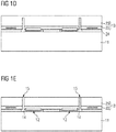
- two trenches 15 are formed within the substrate body 13. They can be formed for example by etching. The two trenches 15 extend through a part of the substrate body 13 in vertical direction z and they are arranged next to the environmental sensors 12. It is also possible that the trenches 15 are formed before applying the bonding material 24.
- a cap body 11 is attached to the bonding material 24.
- the cap body 11 can be connected with the bonding material 24 at elevated temperatures.
- the cap body 11 can comprise silicon, glass, or glass with a coefficient of thermal expansion which is similar to the coefficient of thermal expansion of the substrate body 13.
- Above the environmental sensors 12 and between the cap body 11 and the substrate body 13 two first volumes of gas 14 are formed where each of the first volumes of gas 14 is in direct contact with one of the environmental sensors 12, respectively.
- the membranes 30 of the environmental sensors 12 are advantageously protected at this early stage of the processing. Furthermore, both the surface of the cap body 11 that faces away from the environmental sensors 12 and the surface of the substrate body 13 that faces away from the environmental sensors 12 are flat and easy to handle during processing while the environmental sensors 12 are protected. Therefore, the membrane 30 of the environmental sensor 12 is never exposed to handling during processing.
- FIG 1D it is shown that in the next step the substrate body 13 is thinned, for example by grinding. In this way, the total height of the semiconductor device 10 is reduced.
- the substrate body 13 is further thinned by dry etching such that the trenches 15 are opened from the side of the substrate body 13 which faces away from the environmental sensors 12. Via the first volumes of gas 14 and the trenches 15 the environmental sensors 12 are in contact with the gas of the environment of the semiconductor device 10.
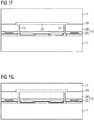
- a closing body 17 is connected with the substrate body 13 at the side of the substrate body 13 which faces away from the environmental sensors 12 via the bonding material 24.
- the closing body 17 can be connected with the substrate body 13 in the same way as the substrate body 13 is connected with the cap body 11.
- the closing body 17 is patterned at one side in such a way that between the closing body 17 and the substrate body 13 a second volume of gas 20 is formed. This means, the closing body 17 comprises a recess at one side.
- the second volume of gas 20 is connected with the two trenches 15.
- the lateral extent of the second volume of gas 20 is slightly larger than the lateral distance between the two trenches 15.
- the cap body 11 is thinned as well, for example by grinding.
- a passivation layer 27 is applied to the side of the cap body 11 which faces away from the substrate body 13.
- the passivation layer 27, the cap body 11, the bonding material 24 and the sealing layer 23 are etched away above the two metal layers 25 of the integrated circuit 22.
- the two metal layers 25 act as etch stop layers.
- the vias 32 are filled with an electrically conductive material 34 and that the two contact areas 31 are electrically contacted with solder balls 28.
- the electrically conductive material 34 can be the same material as the solder balls 28. Consequently, the semiconductor device 10 can be electrically contacted at the side of the cap body 11 which faces away from the substrate body 13.
- a decoupling portion 19 of the substrate body 13 which comprises the two environmental sensors 12 is formed. The decoupling portion 19 is decoupled from the substrate body 13. It is possible that the trenches 15 completely surround the decoupling portion 19 from all lateral sides.
- the decoupling portion 19 is not connected to the closing body 17 as the second volume of gas 20 is arranged between the decoupling portion 19 and the closing body 17.
- the decoupling portion 19 is only connected to the cap body 11 via the bonding material 24 between the cap body 11 and the substrate body 13. Therefore, if external stress is exerted on the semiconductor device 10 the decoupling portion 19 with the two environmental sensors 12 is decoupled from most parts of the semiconductor device 10 and thus it is also decoupled from external stress. Consequently, the environmental sensors 12 are also decoupled from external stress when the semiconductor device 10 is incorporated in a final product. As no or nearly no additional stress is induced on the environmental sensors 12 in comparison to during calibration the accuracy of the environmental sensors 12 is increased.
- the semiconductor device 10 comprises a channel 16 connecting the first volume of gas 14 and the trenches 15 with the environment of the semiconductor device 10 such that the channel 16 is permeable for gases.
- the semiconductor device 10 is air-tight except for the channel 16.
- the channel 16 can be arranged for example within the closing body 17 or between the closing body 17 and the substrate body 13.
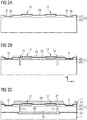
- FIG. 2A an alternative method for forming a semiconductor device 10 is shown.
- FIG 2A an alternative process step after the step shown in figure 1A is depicted.
- the sealing layer 23 and the environmental sensors 12 which are arranged on the substrate 29 are etched away above the two metal layers 25. In this way, two contact areas 31 are formed where the integrated circuit 22 can be electrically contacted.
- the bonding material 24 is applied to the surface of the substrate body 13 on top of the sealing layer 23.
- the bonding material 24 is patterned in such a way that the contact areas 31 and the environmental sensors 12 are free of the bonding material 24.
- an area of the sealing layer 23 around the contact areas 31 and the environmental sensors 12 is free of the bonding material 24.
- two trenches 15 are formed within the substrate body 13 by etching. The trenches 15 extend through a part of the substrate body 13 in vertical direction z and they are arranged next to the environmental sensors 12.
- FIG 2C it is shown that the next steps of the alternative method are the same steps as shown in figures 1C to 1H .
- a passivation layer 27 is applied to the side of the cap body 11 which faces away from the substrate body 13.
- the cap body 11 with the passivation layer 27 is etched away above the contact areas 31, as the bonding material 24 and the sealing layer 23 were already etched away in a previous step.
- the cap body 11 with the passivation layer 27 is etched further in the lateral direction x than the bonding material 24. In this way a stepped structure is formed around the contact areas 31 including the sealing layer 23, the bonding material 24 and the cap body 11 with the passivation layer 27.
- the contact areas 31 are electrically contacted by solder balls 28.
- the solder balls 28 are only in contact with the contact area 31 and do not touch any other part of the semiconductor device 10. Therefore, leakage currents from the solder balls 28 through other areas than the contact areas 31 are avoided.
- FIG 3 shows a top view of an exemplary embodiment of a semiconductor device 10 which is formed by one of the methods shown in figures 1A to 1J and 2A to 2D .
- the top view in figure 3 is not a cut through one plane of the semiconductor device 10 but it shows several parts of the semiconductor device 10 seen from the top.
- Two environmental sensors 12 are arranged on a decoupling portion 19. Each environmental sensor 12 is surrounded by a U-shaped trench 15. Preferably, the two trenches 15 are located very close to each other, this means, they are almost connected with each other.
- a channel 16 is connected with the trenches 15 and the first volume of gas 14 which is arranged above the two environmental sensors 12.
- the channel 16 is arranged within the closing body 17.
- the lateral extent of the decoupling portion 19 gives the approximate lateral extent of the second volume of gas 20 which is also connected to the trenches 15.
- the two environmental sensors 12 are surrounded by the substrate body 13 which can comprise an integrated circuit 22.
- the substrate body 13 comprises the substrate 29 and the integrated circuit 22 with two metal layers 25.
- Two environmental sensors 12 are arranged on top of the substrate body 13.
- the two environmental sensors 12 and the integrated circuit 22 are covered by the sealing layer 23.
- Two vertical trenches 15 are etched in a part of the substrate body 13 next to the environmental sensors 12.
- a bonding material 24 is applied to the sealing layer 23.
- the bonding material 24 is patterned in such a way that it is removed from the area above the membrane 30 and around the membrane 30 and from the trenches 15.
- two vias 32 are formed within the bonding material 24 above the metal layers 25 where the lateral extent of the vias 32 is smaller than the lateral extent of the metal layers 25. It is also possible that the trenches 15 are only formed after applying the bonding material 24.
- the cap body 11 is bonded to the substrate body 13 with the bonding material 24. Furthermore, the cap body 11 is thinned, for example by grinding.
- two vias 32 are etched in the cap body 11 above the vias 32 within the bonding material 24.
- the lateral extent of the vias 32 within the cap body 11 is larger than the lateral extent of the vias 32 within the bonding material 24.
- FIG 4D it is shown that the vias 32 within the bonding material 24 are further etched and the material above the metal layers 25 is etched away within the vias 32 of the bonding material 24.
- This means vias 32 are formed from the side of the cap body 11 facing away from the substrate body 13 towards the metal layers 25 such that contact areas 31 are formed. At the contact areas 31 the integrated circuit 22 can be electrically contacted.
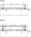
- an isolation layer 33 is deposited on the side of the cap body 11 that faces away from the substrate body 13 and within the vias 32.
- an electrically conductive material 34 is deposited within the vias 32.
- the electrically conductive material 34 can for example comprise Cu or W.
- the vias 32 are not completely filled with the electrically conductive material 34. However, it is also possible that the vias 32 are completely filled with the electrically conductive material 34.
- two back contacts 35 are formed by depositing an electrically conductive material 34 on and around the vias 32.
- Another isolation layer 33 is deposited at the side of the cap body 11 that faces away from the substrate body 13. The isolation layer 33 is patterned in such a way that the back contacts 35 are free of the isolation layer 33.
- the vias 32 are electrically conductive.
- a handling wafer 36 is attached at the side of the cap body 11 that faces away from the substrate body 13. Additionally, the substrate body 13 is thinned at the side that faces away from the cap body 11.
- the substrate body 13 is further thinned by dry etching such that the trenches 15 are opened from the side of the substrate body 13 which faces away from the environmental sensors 12. Via the first volumes of gas 14 and the trenches 15 the environmental sensors 12 are in contact with the gas of the environment of the semiconductor device 10.
- a closing body 17 is connected with the substrate body 13 at the side of the substrate body 13 which faces away from the environmental sensors 12 via a bonding material 24.
- the closing body 17 is patterned at one side in such a way that between the closing body 17 and the substrate body 13 a second volume of gas 20 is formed.
- the second volume of gas 20 is connected with the two trenches 15.
- the closing body 17 is thinned at the side that faces away from the substrate body 13.
- FIG. 5A an alternative method for forming a semiconductor device 10 is shown.
- FIG 5A an alternative process step after the step shown in figure 4A is depicted.
- the bonding material 24 is applied to the sealing layer 23.
- the bonding material 24 is only removed from the area above the membrane 30 and around the membrane 30.
- the two trenches 15 are etched in the substrate body 13 next to the environmental sensors 12.
- the cap body 11 is bonded to the substrate body 13 with the bonding material 24.
- the bonding material 24 and the sealing layer 23 above the two metal layers 25 two vias 32 are formed.
- the two vias 32 extend in vertical direction z and comprise an approximately constant diameter.
- This method shown in figures 5A and 5B can be applied instead of the method shown in figures 4A to 4D if it is possible to etch the bonding material 24 in the step shown in figure 5B . If it is not possible to etch the bonding material 24 because of its material properties a glue or a dry film which can be patterned can be employed as the bonding material 24 in the step shown in figure 4B .
- back contacts 35 and electrically conductive vias 32 are formed as described with figures 4F and 4G .
- FIG 5D it is shown that the electric back contacts 35 are electrically contacted by solder balls 28.
- the closing body 17 is arranged at the side of the substrate body 13 that faces away from the cap body 11 as described with figures 4H to 4J .
- Figure 6A shows a top view of an exemplary embodiment of a semiconductor device 10.
- the top view in figure 6A is not a cut through one plane of the semiconductor device 10 but it shows several parts of the semiconductor device 10 seen from the top.
- Two environmental sensors 12 are arranged on a decoupling portion 19 and they are surrounded by a rectangular shaped trench 15.
- a channel 16 is connected with the trench 15 and with the first volume of gas 14 which is arranged above the two environmental sensors 12.
- the lateral extent of the decoupling portion 19 gives the approximate lateral extent of the second volume of gas 20 which is also connected to the trench 15.
- the two environmental sensors 12 are surrounded by the substrate body 13 which can comprise an integrated circuit 22.
- the rectangular shaped area between the two environmental sensors 12 marks the connection of the decoupling portion 19 to the cap body 11. In this embodiment the decoupling portion 19 is only connected with the cap body 11 but not with the substrate body 13.
- Figure 6B shows a cutaway view of the exemplary embodiment of the semiconductor device 10 depicted in figure 6A .
- the two electrically conductive vias 32 which extend through the cap body 11 are arranged between the two environmental sensors 12 in lateral direction x.
- the two vias 32 can be formed as described with figures 4A to 4G or 5A to 5D .
- the trench 15 laterally surrounds the decoupling portion 19 with the two environmental sensors 12 from all lateral sides.
- the second volume of gas 20 is arranged between the decoupling portion 19 and the closing body 17 such that the decoupling portion 19 and the closing body 17 are not in contact with each other. This means, the decoupling portion 19 is only connected with the cap body 11 but not with the substrate body 13. In this way, the environmental sensors 12 are further decoupled from external stress and a bending of the decoupling portion 19 is avoided.
- FIG. 7A the substrate body 13 with the bonding material 24 is depicted as described with figure 1B .
- the cap body 11 is connected with the substrate body 13 via the bonding material 24.
- the substrate body 13 is thinned such that the trenches 15 are still closed.
- figure 7C it is shown that the substrate body 13 is further thinned by dry etching as described with figure 1E .
- the closing body 17 is connected with the substrate body 13 via direct bonding. Both the substrate body 13 and the closing body 17 comprise silicon. Additionally, the cap body 11 is thinned.
- two vias 32 are etched in the closing body 17 and the substrate body 13 above the metal layers 25. This means, all material above the two metal layers 25 is etched away such that contact areas 31 are formed.
- the two vias 32 extend in vertical direction z and comprise an approximately constant diameter.
- back contacts 35 and electrically conductive vias 32 are formed as described with figures 4E to 4G .
- FIG 7G it is shown that the back contacts 35 are electrically contacted by solder balls 28.
- the vias 32 are formed by etching only through the closing body 17 and the substrate body 13 but not through the bonding material 24. In this way, the etching process can be simplified.
Landscapes
- Engineering & Computer Science (AREA)
- Microelectronics & Electronic Packaging (AREA)
- Computer Hardware Design (AREA)
- Pressure Sensors (AREA)
- Internal Circuitry In Semiconductor Integrated Circuit Devices (AREA)
Abstract
Description
- The present application relates to a semiconductor device.
- Semiconductor devices can comprise environmental sensors as, for example, pressure sensors. Several environmental sensors and especially pressure sensors are sensitive to stress. In order to keep the same conditions as during calibration of the sensors it is desired that no additional stress is exerted on the semiconductor device after the calibration. As in most cases the semiconductor devices are calibrated before they are incorporated into a final product, e.g. a mobile phone, additional stress can be exerted on the semiconductor device within the final product. If the additional stress is transferred to the environmental sensor it is less accurate.
- It is furthermore desired to reduce the package height of semiconductor devices comprising an environmental sensor in order to include the semiconductor devices in mobile phones or other portable devices.
- Additional stress induced on a semiconductor device can be avoided, for example by the use of thick glue layers or thick ceramic substrates. However, in both cases the thickness and also the footprint of the semiconductor device are increased, which is not desirable for applications in mobile phones or other portable devices.
- It is an objective to improve the accuracy of the environmental sensor of the semiconductor device.
- This objective is solved by the independent claim. Further embodiments are subject of dependent claims.
- In one embodiment of the semiconductor device the semiconductor device comprises a cap body. The cap body can be a wafer, a substrate or a bulk material and it can comprise silicon, glass or a semiconductor.
- The semiconductor device further comprises an environmental sensor. The environmental sensor can be a pressure sensor or, for example, a capacitive pressure sensor with a membrane. The cap body can be arranged on top of the environmental sensor. It is also possible that the semiconductor device comprises several environmental sensors.
- The semiconductor device further comprises a substrate body. The substrate body can be a wafer, a substrate or a bulk material and it can comprise silicon or glass. The substrate body can comprise an integrated circuit and a substrate. It is also possible that the substrate body comprises glass with a coefficient of thermal expansion which is similar to the coefficient of thermal expansion of the cap body. The cap body and the substrate body can be of the same material or they can comprise different materials. The environmental sensor is arranged on top of the substrate body, for example on top of the integrated circuit.
- The semiconductor device further comprises a first volume of gas. The environmental sensor and the first volume of gas are arranged between the substrate body and the cap body in a vertical direction which is perpendicular to the main plane of extension of the substrate body. The first volume of gas can be arranged above the environmental sensor in vertical direction and around the environmental sensor.
- The semiconductor device further comprises a trench extending through at least a part of the substrate body in vertical direction, the trench being connected to the volume of gas and the vertical direction being perpendicular to lateral directions that are parallel to the main plane of extension of the semiconductor device. The trench can be arbitrarily shaped within the substrate body. The trench can further have the shape of a line or it can be L-shaped or U-shaped within a plane which is parallel to the main plane of extension of the semiconductor device. It is also possible that the trench has a rectangular or a square shape. This means, the trench can surround an area or a volume of the substrate body in the lateral directions. The trench can comprise an approximately uniform depth in vertical direction.
- The trench can be formed within the substrate body by etching. For example, the trench can be etched in the substrate body before the cap body is bonded to the substrate body. The trench is not filled with a solid material but only with the gas surrounding the semiconductor device.
- It is also possible that the semiconductor device comprises several trenches. The several trenches can surround the environmental sensor from different sides.
- In a preferred embodiment the trench is arranged next to or around the environmental sensor. In this way, the environmental sensor is decoupled from the substrate body. The environmental sensor can be arranged on the substrate body, however, by forming the trench next to or around the environmental sensor the environmental sensor is less connected to the substrate body. Consequently, if stress is induced on the substrate body in vertical or in lateral directions the environmental sensor can be partially or mostly decoupled from this stress or the stress is at least not completely transferred to the environmental sensor. Also, if the semiconductor device is bent this external stress is not completely transferred to the environmental sensor.
- The semiconductor device further comprises a channel connecting the first volume of gas and the trench with the environment of the semiconductor device such that the channel is permeable for gases. "Permeable for gases" in this case means that gases from the environment of the semiconductor device can reach the first volume of gas within the semiconductor device and the other way around. The channel can be arranged next to the environmental sensor in a lateral direction and the channel can extend in a lateral direction. The channel can have a diameter which is small in comparison to the lateral extension of the semiconductor device and it can also be a channel with a lateral extension which is similar to the lateral extension of the semiconductor device.
- The substrate body and the cap body can be connected with each other via a bonding material. The bonding material is arranged between the substrate body and the cap body, and the bonding material comprises at least one of the following: a polymer, a photo-definable glue, a non-photosensitive glue, a metal, an oxide, a nitride. The bonding material can be applied on the substrate body as a foil or via spin coating in the case of glue. The cap body and the substrate body can be connected with each other by, for example, gluing, fusion bonding or eutectic bonding. By connecting the cap body and the substrate body an airtight connection can be formed, except for the channel. In another embodiment the bonding material is applied by Physical Vapor Deposition (PVD), Chemical Vapor Deposition (CVD), Plasma Enhanced Chemical Vapor Deposition (PECVD) and or Atomic Layer Deposition (ALD). The channel can be formed in the bonding material, therefore the bonding material can be patterned by lithographic etching. The semiconductor device can comprise several channels within the bonding material.
- It is also possible that the channel is formed at another position in the semiconductor device.
- Since the cap body is arranged on top of the substrate body and the environmental sensor the thickness of the semiconductor device is increased and also the stiffness of the semiconductor device is increased. Therefore, additional vertical stress on the environmental sensor or on integrated circuits in the semiconductor device is reduced. Additional stress on the environmental sensor can be further reduced by arranging the trench next to or around the environmental sensor. In this way, the environmental sensor is less connected to the substrate body and decoupled from the substrate body and external stress. Consequently, the environmental sensor is also decoupled from external stress when the semiconductor device is incorporated in a final product. As no or nearly no additional stress is induced on the environmental sensor in comparison to during calibration the accuracy of the environmental sensor is increased.
- Furthermore, the environmental sensor is protected by the cap body during processing. Moreover, the substrate body can be thin enough to introduce an electrically conductive via or other electrical contacts in the substrate body since the cap body increases the total thickness of the semiconductor device.
- By forming a stiff package without the use of glue layers or thick substrates, the footprint and the cost of the device can be reduced.
- In one embodiment of the semiconductor device the environmental sensor comprises a pressure sensor. The pressure sensor can for example be a capacitive pressure sensor. The capacitive pressure sensor can comprise a cavity below a membrane. The advantages of capacitive pressure sensing are a low power consumption, a high sensitivity and a high resolution. Furthermore, it can be integrated directly on top of an integrated circuit. With this, the footprint of the device can be reduced.
- In one embodiment of the semiconductor device a closing body is arranged at the side of the substrate body that faces away from the environmental sensor. This means, the substrate body is arranged between the cap body and the closing body. The closing body can be a wafer, a substrate or a bulk material and it can comprise silicon or glass. It is also possible that the closing body comprises glass with a coefficient of thermal expansion which is similar to the coefficient of thermal expansion of the cap body and the substrate. The closing body, the cap body and the substrate body can be of the same material or they can comprise different materials. The closing body can be connected with the substrate body in the same way as the cap body is connected with the substrate body. It is also possible that the closing body is bonded to the substrate body by one of the bond materials or methods described above.
- Preferably, the substrate body is thinned before the closing body is connected with the substrate body in order to reduce the total thickness of the semiconductor device.
- In one embodiment of the semiconductor device the channel is arranged within the closing body. This means, the channel can be a channel which is completely arranged within the closing body. It is also possible that the channel is arranged between the substrate body and the closing body in the semiconductor device by patterning the closing body in such a way that the channel is formed within the closing body. Consequently, the bonding material between the substrate body and the cap body does not have to be patterned in order to form the channel.
- In other embodiments it is possible that the channel is arranged between the substrate body and the cap body for example within a bonding material. It is also possible that the channel is formed in the cap body or in the substrate body.
- In one embodiment of the semiconductor device the closing body comprises at least one electrically conductive via. The electrically conductive via can extend in a vertical direction from the top side of the closing body, which faces away from the substrate body, towards the substrate body. The electrically conductive via electrically contacts the environmental sensor or another electrical contact, for example a back contact of an integrated circuit. The electrically conductive via can be a through silicon via which is formed by patterning of the closing body, for example by etching. A via patterned in the closing body can be coated with an isolation material and with an electrically conductive material to contact the environmental sensor.
- If the electrical contact of the environmental sensor or the back contact of the integrated circuit is not arranged on the side of the substrate body facing away from the closing body, the electrically conductive via also extends through the substrate body towards the electrical contact of the environmental sensor or the back contact of the integrated circuit. If the closing body and the substrate body are connected via direct bonding, advantageously in this embodiment only the closing body or the closing body and the substrate body need to be etched in order to form an electrically conductive via but no other material as for example a bonding material. For other materials than the closing body and the substrate body the etching process can be more complicated.
- In one embodiment of the semiconductor device the trench is arranged next to the environmental sensor in lateral direction. This means the trench is not positioned below or above the environmental sensor in a vertical direction. It is also possible that the trench is arranged next to the environmental sensor in different lateral directions. With the trench being arranged next to the environmental sensor, the environmental sensor is decoupled from the substrate body and thus it is also decoupled from external stress.
- In one embodiment of the semiconductor device the environmental sensor is in direct contact with the first volume of gas. This means, the first volume of gas can be arranged above the environmental sensor in vertical direction or around the environmental sensor. "In direct contact" further means that if the environmental sensor comprises a pressure sensor, it can measure the pressure in the first volume of gas which is similar or the same as the pressure in the environment of the semiconductor device, since the first volume of gas is connected with the channel. Thus, the pressure sensor can advantageously measure the pressure in the environment of the semiconductor device.
- In one embodiment of the semiconductor device the trench at least partially surrounds a decoupling portion in lateral directions, where the decoupling portion comprises the environmental sensor. The decoupling portion can be a volume of material which comprises for example a part of the substrate body and the environmental sensor. The decoupling portion can for example be a cuboid. The trench directly borders the decoupling portion such that the trench gives the limit of the decoupling portion. If for example the trench is arranged around the environmental sensor the decoupling portion is the volume of material that is surrounded by the trench. The decoupling portion is at least partially decoupled from the substrate body in order to reduce external stress on the environmental sensor. It is possible that the trench is formed in such a way that the decoupling portion is connected to the substrate body. The more the decoupling portion is decoupled from the substrate body the less external stress is exerted on the environmental sensor. Preferably, there is only one connection point between the decoupling portion and the substrate body.
- In one embodiment of the semiconductor device a second volume of gas is arranged at the side of the decoupling portion which faces away from the environmental sensor. This means, the second volume of gas can be arranged between the substrate body and the closing body. The lateral extent of the second volume of gas can be the same as the lateral extent of the decoupling portion. For forming the second volume of gas the closing body can be patterned or comprise one or more recesses. The second volume of gas can be connected with the trench and with the channel such that the second volume of gas is also connected to the environment of the semiconductor device.
- With the second volume of gas being arranged at the side of the decoupling portion which faces away from the environmental sensor the decoupling portion is further decoupled from the substrate body and also from the closing body. Therefore, the environmental sensor is further decoupled from external stress.
- In one embodiment of the semiconductor device the decoupling portion comprises a further environmental sensor. The further environmental sensor can be arranged next to the environmental sensor. The further environmental sensor can be the same type of sensor as the environmental sensor. The trench is arranged next to or around the two environmental sensors. It is also possible, that two trenches are arranged next to or around the two environmental sensors. Advantageously, with two environmental sensors it is possible to arrange the environmental sensors and the one or more trenches in a symmetrical arrangement.
- In one embodiment of the semiconductor device the decoupling portion is connected to the cap body. The decoupling portion can be connected to the cap body with a bonding material between the cap body and the substrate body. It is possible that the decoupling portion is only connected to the cap body and not to the substrate body. In this way, the environmental sensor is further decoupled from external stress.
- In one embodiment of the semiconductor device the environmental sensor is arranged on an integrated circuit. The environmental sensor can be arranged on top of the final passivation layer of a complementary metal oxide semiconductor device readout circuit. With this arrangement the total lateral size of the semiconductor device can be reduced. Moreover, the additional stress is also minimized for the integrated circuit and not only for the environmental sensor since the integrated circuit is protected by the substrate body and the cap body.
- In one embodiment the semiconductor device is airtight except for the channel. This means that the semiconductor device comprises no other openings or channels than the at least one channel which connects the first volume of gas with the environment of the semiconductor device. In this case "airtight" means that only the at least one channel is permeable for gases from the environment of the semiconductor device to the first volume of gas and the other way around. With this arrangement a pressure sensor in the semiconductor device can sense the pressure of the gas surrounding the semiconductor device. The opening of the channel towards the environment of the semiconductor device can be positioned at a side surface of the semiconductor device. This arrangement is advantageous for the processing of the semiconductor device since it can be vacuum-picked at the cap body or the substrate body and the respective other side of the semiconductor device can be processed.
- In one embodiment of the semiconductor device the cap body comprises at least one electrically conductive via. The electrically conductive via can extend within the cap body in vertical direction from the side of the environmental sensor towards a bottom side of the cap body which faces away from the substrate body. The electrically conductive via electrically contacts the environmental sensor or another electrical contact, for example a back contact of an integrated circuit of the substrate body. The electrically conductive via can be a through silicon via which is formed by patterning of the cap body, for example by etching. The electrically conductive via can be electrically contacted on the bottom side of the semiconductor device by a solder ball.
- The following description of figures may further illustrate and explain exemplary embodiments. Components that are functionally identical or have an identical effect are denoted by identical references. Identical or effectively identical components might be described only with respect to the figures where they occur first. Their description is not necessarily repeated in successive figures.
- With
figures 1A to 1J , a method for forming an exemplary embodiment of a semiconductor device is described. - In
figures 2A to 2D , another method for forming an exemplary embodiment of a semiconductor device is shown. -
Figure 3 shows a top view of an exemplary embodiment of the semiconductor device. - With
figures 4A to 4L , another method for forming an exemplary embodiment of a semiconductor device is described. - In
figures 5A to 5D , another method for forming an exemplary embodiment of a semiconductor device is shown. -
Figure 6A shows a top view of an exemplary embodiment of the semiconductor device. -
Figure 6B shows a cutaway view of an exemplary embodiment of the semiconductor device. - With
figures 7A to 7G , another method for forming an exemplary embodiment of a semiconductor device is described. -
Figure 1A shows a processing step for forming asemiconductor device 10. A cutaway view of asubstrate body 13 is shown which comprises anintegrated circuit 22 which can be for example a complementary metal oxide semiconductor device. Theintegrated circuit 22 is arranged on top of asubstrate 29 in a vertical direction z where thesubstrate 29 is comprised by thesubstrate body 13 and it can comprise silicon or glass. The vertical direction z is perpendicular to the main plane of extension of thesemiconductor device 10. Theintegrated circuit 22 comprises two metal layers 25. It is also possible that theintegrated circuit 22 comprises more than twometal layers 25 or other electrical contacts. On top of theintegrated circuit 22 twoenvironmental sensors 12 are arranged. In this embodiment theenvironmental sensors 12 are capacitive pressure sensors. By arranging theenvironmental sensors 12 on top of theintegrated circuit 22 instead of next to it, the footprint of thesemiconductor device 10 is reduced. Theenvironmental sensors 12 are arranged between the twometal layers 25 in a lateral direction x which is perpendicular to the vertical direction z. In this exemplary embodiment theenvironmental sensors 12 comprise acavity 26 below amembrane 30. Theenvironmental sensors 12 are electrically connected to theintegrated circuit 22. In order to close the cavity 26 asealing layer 23 is deposited on top of the releasedmembrane 30 and around themembrane 30 such that themembrane 30 is sensitive to differences in pressure. Thesealing layer 23 can comprise silicon nitride. - In
figure 1B , it is shown that abonding material 24 is applied to thesealing layer 23. Thebonding material 24 can comprise a photo-sensitive glue layer which can be polymer based or polyimide based. By applying a mask, thebonding material 24 is patterned in such a way that it is removed from the area above themembrane 30 and around themembrane 30. Additionally, twotrenches 15 are formed within thesubstrate body 13. They can be formed for example by etching. The twotrenches 15 extend through a part of thesubstrate body 13 in vertical direction z and they are arranged next to theenvironmental sensors 12. It is also possible that thetrenches 15 are formed before applying thebonding material 24. - As shown in
figure 1C in a next step acap body 11 is attached to thebonding material 24. Thecap body 11 can be connected with thebonding material 24 at elevated temperatures. Thecap body 11 can comprise silicon, glass, or glass with a coefficient of thermal expansion which is similar to the coefficient of thermal expansion of thesubstrate body 13. Above theenvironmental sensors 12 and between thecap body 11 and thesubstrate body 13 two first volumes ofgas 14 are formed where each of the first volumes ofgas 14 is in direct contact with one of theenvironmental sensors 12, respectively. Themembranes 30 of theenvironmental sensors 12 are advantageously protected at this early stage of the processing. Furthermore, both the surface of thecap body 11 that faces away from theenvironmental sensors 12 and the surface of thesubstrate body 13 that faces away from theenvironmental sensors 12 are flat and easy to handle during processing while theenvironmental sensors 12 are protected. Therefore, themembrane 30 of theenvironmental sensor 12 is never exposed to handling during processing. - In
figure 1D it is shown that in the next step thesubstrate body 13 is thinned, for example by grinding. In this way, the total height of thesemiconductor device 10 is reduced. - As shown in
figure 1E thesubstrate body 13 is further thinned by dry etching such that thetrenches 15 are opened from the side of thesubstrate body 13 which faces away from theenvironmental sensors 12. Via the first volumes ofgas 14 and thetrenches 15 theenvironmental sensors 12 are in contact with the gas of the environment of thesemiconductor device 10. - In
figure 1F it is shown that in a next step a closingbody 17 is connected with thesubstrate body 13 at the side of thesubstrate body 13 which faces away from theenvironmental sensors 12 via thebonding material 24. The closingbody 17 can be connected with thesubstrate body 13 in the same way as thesubstrate body 13 is connected with thecap body 11. The closingbody 17 is patterned at one side in such a way that between the closingbody 17 and the substrate body 13 a second volume ofgas 20 is formed. This means, the closingbody 17 comprises a recess at one side. The second volume ofgas 20 is connected with the twotrenches 15. The lateral extent of the second volume ofgas 20 is slightly larger than the lateral distance between the twotrenches 15. - In
figure 1G it is shown that in the next step the closingbody 17 is thinned, for example by grinding. - As shown in
figure 1H thecap body 11 is thinned as well, for example by grinding. - As shown in
figure 1I in a next step apassivation layer 27 is applied to the side of thecap body 11 which faces away from thesubstrate body 13. In order to form an electric contact to theintegrated circuit 22; thepassivation layer 27, thecap body 11, thebonding material 24 and thesealing layer 23 are etched away above the twometal layers 25 of theintegrated circuit 22. This means, two vias 32 and twocontact areas 31 are formed next to theenvironmental sensors 12 in lateral direction x. The twometal layers 25 act as etch stop layers. - In
figure 1J it is shown that thevias 32 are filled with an electricallyconductive material 34 and that the twocontact areas 31 are electrically contacted withsolder balls 28. The electricallyconductive material 34 can be the same material as thesolder balls 28. Consequently, thesemiconductor device 10 can be electrically contacted at the side of thecap body 11 which faces away from thesubstrate body 13. By forming the twotrenches 15 and the second volume ofgas 20, adecoupling portion 19 of thesubstrate body 13 which comprises the twoenvironmental sensors 12 is formed. Thedecoupling portion 19 is decoupled from thesubstrate body 13. It is possible that thetrenches 15 completely surround thedecoupling portion 19 from all lateral sides. It is also possible that thedecoupling portion 19 is not connected to the closingbody 17 as the second volume ofgas 20 is arranged between thedecoupling portion 19 and the closingbody 17. This means, it is possible that thedecoupling portion 19 is only connected to thecap body 11 via thebonding material 24 between thecap body 11 and thesubstrate body 13. Therefore, if external stress is exerted on thesemiconductor device 10 thedecoupling portion 19 with the twoenvironmental sensors 12 is decoupled from most parts of thesemiconductor device 10 and thus it is also decoupled from external stress. Consequently, theenvironmental sensors 12 are also decoupled from external stress when thesemiconductor device 10 is incorporated in a final product. As no or nearly no additional stress is induced on theenvironmental sensors 12 in comparison to during calibration the accuracy of theenvironmental sensors 12 is increased. - It is not shown in
figure 1J that thesemiconductor device 10 comprises achannel 16 connecting the first volume ofgas 14 and thetrenches 15 with the environment of thesemiconductor device 10 such that thechannel 16 is permeable for gases. This means, thesemiconductor device 10 is air-tight except for thechannel 16. Thechannel 16 can be arranged for example within the closingbody 17 or between the closingbody 17 and thesubstrate body 13. - With
figures 2A to 2D an alternative method for forming asemiconductor device 10 is shown. Infigure 2A an alternative process step after the step shown infigure 1A is depicted. After the deposition of thesealing layer 23 on theintegrated circuit 22 and theenvironmental sensors 12 which are arranged on thesubstrate 29, thesealing layer 23 and a part of theintegrated circuit 22 are etched away above the two metal layers 25. In this way, twocontact areas 31 are formed where theintegrated circuit 22 can be electrically contacted. - In
figure 2B it is shown that thebonding material 24 is applied to the surface of thesubstrate body 13 on top of thesealing layer 23. Thebonding material 24 is patterned in such a way that thecontact areas 31 and theenvironmental sensors 12 are free of thebonding material 24. Furthermore, an area of thesealing layer 23 around thecontact areas 31 and theenvironmental sensors 12 is free of thebonding material 24. Additionally, twotrenches 15 are formed within thesubstrate body 13 by etching. Thetrenches 15 extend through a part of thesubstrate body 13 in vertical direction z and they are arranged next to theenvironmental sensors 12. - In
figure 2C it is shown that the next steps of the alternative method are the same steps as shown infigures 1C to 1H . After the thinning of the cap body 11 apassivation layer 27 is applied to the side of thecap body 11 which faces away from thesubstrate body 13. In contrast to the method shown infigures 1A to 1J in this case only thecap body 11 with thepassivation layer 27 is etched away above thecontact areas 31, as thebonding material 24 and thesealing layer 23 were already etched away in a previous step. Thecap body 11 with thepassivation layer 27 is etched further in the lateral direction x than thebonding material 24. In this way a stepped structure is formed around thecontact areas 31 including thesealing layer 23, thebonding material 24 and thecap body 11 with thepassivation layer 27. - As shown in
figure 2D thecontact areas 31 are electrically contacted bysolder balls 28. However, in this case thesolder balls 28 are only in contact with thecontact area 31 and do not touch any other part of thesemiconductor device 10. Therefore, leakage currents from thesolder balls 28 through other areas than thecontact areas 31 are avoided. -
Figure 3 shows a top view of an exemplary embodiment of asemiconductor device 10 which is formed by one of the methods shown infigures 1A to 1J and 2A to 2D . The top view infigure 3 is not a cut through one plane of thesemiconductor device 10 but it shows several parts of thesemiconductor device 10 seen from the top. Twoenvironmental sensors 12 are arranged on adecoupling portion 19. Eachenvironmental sensor 12 is surrounded by aU-shaped trench 15. Preferably, the twotrenches 15 are located very close to each other, this means, they are almost connected with each other. Achannel 16 is connected with thetrenches 15 and the first volume ofgas 14 which is arranged above the twoenvironmental sensors 12. Thechannel 16 is arranged within the closingbody 17. The lateral extent of thedecoupling portion 19 gives the approximate lateral extent of the second volume ofgas 20 which is also connected to thetrenches 15. The twoenvironmental sensors 12 are surrounded by thesubstrate body 13 which can comprise anintegrated circuit 22. - With
figures 4A to 4L , another method for forming an exemplary embodiment of thesemiconductor device 10 is described. Infigure 4A it is shown that thesubstrate body 13 comprises thesubstrate 29 and theintegrated circuit 22 with two metal layers 25. Twoenvironmental sensors 12 are arranged on top of thesubstrate body 13. The twoenvironmental sensors 12 and theintegrated circuit 22 are covered by thesealing layer 23. Twovertical trenches 15 are etched in a part of thesubstrate body 13 next to theenvironmental sensors 12. - In
figure 4B , it is shown that abonding material 24 is applied to thesealing layer 23. By applying a mask, thebonding material 24 is patterned in such a way that it is removed from the area above themembrane 30 and around themembrane 30 and from thetrenches 15. Additionally, two vias 32 are formed within thebonding material 24 above the metal layers 25 where the lateral extent of thevias 32 is smaller than the lateral extent of the metal layers 25. It is also possible that thetrenches 15 are only formed after applying thebonding material 24. - As shown in
figure 4C in a next step thecap body 11 is bonded to thesubstrate body 13 with thebonding material 24. Furthermore, thecap body 11 is thinned, for example by grinding. - In the next step as shown in
figure 4D twovias 32 are etched in thecap body 11 above thevias 32 within thebonding material 24. The lateral extent of thevias 32 within thecap body 11 is larger than the lateral extent of thevias 32 within thebonding material 24. - In
figure 4D it is shown that thevias 32 within thebonding material 24 are further etched and the material above the metal layers 25 is etched away within thevias 32 of thebonding material 24. This meansvias 32 are formed from the side of thecap body 11 facing away from thesubstrate body 13 towards the metal layers 25 such thatcontact areas 31 are formed. At thecontact areas 31 the integratedcircuit 22 can be electrically contacted. - As shown in
figure 4F anisolation layer 33 is deposited on the side of thecap body 11 that faces away from thesubstrate body 13 and within thevias 32. - In
figure 4G it is shown that an electricallyconductive material 34 is deposited within thevias 32. The electricallyconductive material 34 can for example comprise Cu or W. Thevias 32 are not completely filled with the electricallyconductive material 34. However, it is also possible that thevias 32 are completely filled with the electricallyconductive material 34. At the side of thecap body 11 that faces away from thesubstrate body 13 twoback contacts 35 are formed by depositing an electricallyconductive material 34 on and around thevias 32. Anotherisolation layer 33 is deposited at the side of thecap body 11 that faces away from thesubstrate body 13. Theisolation layer 33 is patterned in such a way that theback contacts 35 are free of theisolation layer 33. Thus, thevias 32 are electrically conductive. - As shown in
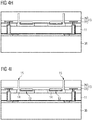
figure 4H in a next step a handlingwafer 36 is attached at the side of thecap body 11 that faces away from thesubstrate body 13. Additionally, thesubstrate body 13 is thinned at the side that faces away from thecap body 11. - As shown in
figure 4I thesubstrate body 13 is further thinned by dry etching such that thetrenches 15 are opened from the side of thesubstrate body 13 which faces away from theenvironmental sensors 12. Via the first volumes ofgas 14 and thetrenches 15 theenvironmental sensors 12 are in contact with the gas of the environment of thesemiconductor device 10. - In
figure 4J it is shown that in a next step a closingbody 17 is connected with thesubstrate body 13 at the side of thesubstrate body 13 which faces away from theenvironmental sensors 12 via abonding material 24. The closingbody 17 is patterned at one side in such a way that between the closingbody 17 and the substrate body 13 a second volume ofgas 20 is formed. The second volume ofgas 20 is connected with the twotrenches 15. Moreover, the closingbody 17 is thinned at the side that faces away from thesubstrate body 13. - In a next step as shown in
figure 4K the handlingwafer 36 is removed. - In
figure 4L it is shown that theback contacts 35 are electrically contacted bysolder balls 28. - With
figures 5A to 5D an alternative method for forming asemiconductor device 10 is shown. Infigure 5A an alternative process step after the step shown infigure 4A is depicted. Thebonding material 24 is applied to thesealing layer 23. In difference tofigure 4B , thebonding material 24 is only removed from the area above themembrane 30 and around themembrane 30. The twotrenches 15 are etched in thesubstrate body 13 next to theenvironmental sensors 12. - As shown in
figure 5B thecap body 11 is bonded to thesubstrate body 13 with thebonding material 24. By etching thecap body 11, thebonding material 24 and thesealing layer 23 above the twometal layers 25 twovias 32 are formed. The two vias 32 extend in vertical direction z and comprise an approximately constant diameter. This method shown infigures 5A and 5B can be applied instead of the method shown infigures 4A to 4D if it is possible to etch thebonding material 24 in the step shown infigure 5B . If it is not possible to etch thebonding material 24 because of its material properties a glue or a dry film which can be patterned can be employed as thebonding material 24 in the step shown infigure 4B . - In
figure 5C it is shown thatback contacts 35 and electricallyconductive vias 32 are formed as described withfigures 4F and 4G . - In
figure 5D it is shown that theelectric back contacts 35 are electrically contacted bysolder balls 28. The closingbody 17 is arranged at the side of thesubstrate body 13 that faces away from thecap body 11 as described withfigures 4H to 4J . -
Figure 6A shows a top view of an exemplary embodiment of asemiconductor device 10. The top view infigure 6A is not a cut through one plane of thesemiconductor device 10 but it shows several parts of thesemiconductor device 10 seen from the top. Twoenvironmental sensors 12 are arranged on adecoupling portion 19 and they are surrounded by a rectangular shapedtrench 15. Achannel 16 is connected with thetrench 15 and with the first volume ofgas 14 which is arranged above the twoenvironmental sensors 12. The lateral extent of thedecoupling portion 19 gives the approximate lateral extent of the second volume ofgas 20 which is also connected to thetrench 15. The twoenvironmental sensors 12 are surrounded by thesubstrate body 13 which can comprise anintegrated circuit 22. The rectangular shaped area between the twoenvironmental sensors 12 marks the connection of thedecoupling portion 19 to thecap body 11. In this embodiment thedecoupling portion 19 is only connected with thecap body 11 but not with thesubstrate body 13. -
Figure 6B shows a cutaway view of the exemplary embodiment of thesemiconductor device 10 depicted infigure 6A . The two electricallyconductive vias 32 which extend through thecap body 11 are arranged between the twoenvironmental sensors 12 in lateral direction x. The two vias 32 can be formed as described withfigures 4A to 4G or 5A to 5D . Thetrench 15 laterally surrounds thedecoupling portion 19 with the twoenvironmental sensors 12 from all lateral sides. The second volume ofgas 20 is arranged between thedecoupling portion 19 and the closingbody 17 such that thedecoupling portion 19 and the closingbody 17 are not in contact with each other. This means, thedecoupling portion 19 is only connected with thecap body 11 but not with thesubstrate body 13. In this way, theenvironmental sensors 12 are further decoupled from external stress and a bending of thedecoupling portion 19 is avoided. - With
figures 7A to 7G , another method for forming an exemplary embodiment of thesemiconductor device 10 is described. Infigure 7A thesubstrate body 13 with thebonding material 24 is depicted as described withfigure 1B . - In a next step as shown in
figure 7B thecap body 11 is connected with thesubstrate body 13 via thebonding material 24. Thesubstrate body 13 is thinned such that thetrenches 15 are still closed. - In
figure 7C it is shown that thesubstrate body 13 is further thinned by dry etching as described withfigure 1E . - In
figure 7D it is shown that the closingbody 17 is connected with thesubstrate body 13 via direct bonding. Both thesubstrate body 13 and the closingbody 17 comprise silicon. Additionally, thecap body 11 is thinned. - As shown in
figure 7E two vias 32 are etched in the closingbody 17 and thesubstrate body 13 above the metal layers 25. This means, all material above the twometal layers 25 is etched away such thatcontact areas 31 are formed. The two vias 32 extend in vertical direction z and comprise an approximately constant diameter. - In a next step as shown in
figure 7F backcontacts 35 and electricallyconductive vias 32 are formed as described withfigures 4E to 4G . - In
figure 7G it is shown that theback contacts 35 are electrically contacted bysolder balls 28. In this alternative method described withfigures 7A to 7G thevias 32 are formed by etching only through the closingbody 17 and thesubstrate body 13 but not through thebonding material 24. In this way, the etching process can be simplified. -
- 10:
- semiconductor device
- 11:
- cap body
- 12:
- environmental sensor
- 13:
- substrate body
- 14:
- first volume of gas
- 15:
- trench
- 16:
- channel
- 17:
- closing body
- 19:
- decoupling portion
- 20:
- second volume of gas
- 21:
- further environmental sensor
- 22:
- integrated circuit
- 23:
- sealing layer
- 24:
- bonding material
- 25:
- metal layer
- 26:
- cavity
- 27:
- passivation layer
- 28:
- solder ball
- 29:
- substrate
- 30:
- membrane
- 31:
- contact area
- 32:
- via
- 33:
- isolation layer
- 34:
- electrically conductive material
- 35:
- back contact
- 36:
- handling wafer
- x:
- lateral direction
- z:
- vertical direction
Claims (14)
- Semiconductor device (10), comprising:- a cap body (11),- an environmental sensor (12),- a substrate body (13),- a first volume of gas (14),- a trench (15) extending through at least a part of the substrate body (13) in a vertical direction (z), the trench (15) being connected to the first volume of gas (14) and the vertical direction (z) being perpendicular to lateral directions (x) that are parallel to the main plane of extension of the semiconductor device (10), and- a channel (16) connecting the first volume of gas (14) and the trench (15) with the environment of the semiconductor device (10) such that the channel (16) is permeable for gases,wherein- the environmental sensor (12) and the first volume of gas (14) are arranged between the cap body (11) and the substrate body (13) in vertical direction (z).
- Semiconductor device (10) according to claim 1, wherein the environmental sensor (12) comprises a pressure sensor.
- Semiconductor device (10) according to one of the preceding claims, wherein a closing body (17) is arranged at the side of the substrate body (13) that faces away from the environmental sensor (12).
- Semiconductor device (10) according to the preceding claim, wherein the channel (16) is arranged within the closing body (17).
- Semiconductor device (10) according to one of claims 3 or 4, wherein the closing body (17) comprises at least one electrically conductive via (32).
- Semiconductor device (10) according to one of the preceding claims, wherein the trench (15) is arranged next to the environmental sensor (12) in lateral direction (x).
- Semiconductor device (10) according to one of the preceding claims, wherein the environmental sensor (12) is in direct contact with the first volume of gas (14).
- Semiconductor device (10) according to one of the preceding claims, wherein the trench (15) at least partially surrounds a decoupling portion (19) in lateral directions (x), where the decoupling portion (19) comprises the environmental sensor (12).
- Semiconductor device (10) according to the preceding claim, wherein a second volume of gas (20) is arranged at the side of the decoupling portion (19) which faces away from the environmental sensor (12).
- Semiconductor device (10) according to one of claims 8 to 9, wherein the decoupling portion (19) comprises a further environmental sensor (12).
- Semiconductor device (10) according to one of claims 8 or 10, wherein the decoupling portion (19) is connected to the cap body (11).
- Semiconductor device (10) according to one of the preceding claims, wherein the environmental sensor (12) is arranged on an integrated circuit (22).
- Semiconductor device (10) according to one of the preceding claims, wherein the semiconductor device (10) is air-tight except for the channel (16).
- Semiconductor device (10) according to one of the preceding claims, wherein the cap body (11) comprises at least one electrically conductive via (32).
Priority Applications (1)
| Application Number | Priority Date | Filing Date | Title |
|---|---|---|---|
| EP17164598.9A EP3385218B1 (en) | 2017-04-03 | 2017-04-03 | Semiconductor device comprising environmental sensor |
Applications Claiming Priority (1)
| Application Number | Priority Date | Filing Date | Title |
|---|---|---|---|
| EP17164598.9A EP3385218B1 (en) | 2017-04-03 | 2017-04-03 | Semiconductor device comprising environmental sensor |
Publications (2)
| Publication Number | Publication Date |
|---|---|
| EP3385218A1 true EP3385218A1 (en) | 2018-10-10 |
| EP3385218B1 EP3385218B1 (en) | 2021-10-13 |
Family
ID=58489533
Family Applications (1)
| Application Number | Title | Priority Date | Filing Date |
|---|---|---|---|
| EP17164598.9A Active EP3385218B1 (en) | 2017-04-03 | 2017-04-03 | Semiconductor device comprising environmental sensor |
Country Status (1)
| Country | Link |
|---|---|
| EP (1) | EP3385218B1 (en) |
Cited By (2)
| Publication number | Priority date | Publication date | Assignee | Title |
|---|---|---|---|---|
| CN111825054A (en) * | 2019-04-18 | 2020-10-27 | 英飞凌科技股份有限公司 | Stress decoupling and particle filter integration |
| CN113526450A (en) * | 2020-04-21 | 2021-10-22 | 英飞凌科技股份有限公司 | Sensor device with a gas-permeable cover and associated production method |
Citations (2)
| Publication number | Priority date | Publication date | Assignee | Title |
|---|---|---|---|---|
| DE102015116353A1 (en) * | 2014-10-31 | 2016-05-04 | Stmicroelectronics S.R.L. | Microintegrated encapsulated MEMS sensor with mechanical decoupling and manufacturing process therefor |
| US20160370242A1 (en) * | 2015-06-22 | 2016-12-22 | Stmicroelectronics S.R.L. | Pressure sensor generating a transduced signal with reduced ambient temperature dependence, and manufacturing method thereof |
-
2017
- 2017-04-03 EP EP17164598.9A patent/EP3385218B1/en active Active
Patent Citations (2)
| Publication number | Priority date | Publication date | Assignee | Title |
|---|---|---|---|---|
| DE102015116353A1 (en) * | 2014-10-31 | 2016-05-04 | Stmicroelectronics S.R.L. | Microintegrated encapsulated MEMS sensor with mechanical decoupling and manufacturing process therefor |
| US20160370242A1 (en) * | 2015-06-22 | 2016-12-22 | Stmicroelectronics S.R.L. | Pressure sensor generating a transduced signal with reduced ambient temperature dependence, and manufacturing method thereof |
Cited By (4)
| Publication number | Priority date | Publication date | Assignee | Title |
|---|---|---|---|---|
| CN111825054A (en) * | 2019-04-18 | 2020-10-27 | 英飞凌科技股份有限公司 | Stress decoupling and particle filter integration |
| CN111825054B (en) * | 2019-04-18 | 2024-06-07 | 英飞凌科技股份有限公司 | Stress decoupling and particle filter integration |
| CN113526450A (en) * | 2020-04-21 | 2021-10-22 | 英飞凌科技股份有限公司 | Sensor device with a gas-permeable cover and associated production method |
| US12122667B2 (en) | 2020-04-21 | 2024-10-22 | Infineon Technologies Ag | Sensor devices with gas-permeable cover and associated production methods |
Also Published As
| Publication number | Publication date |
|---|---|
| EP3385218B1 (en) | 2021-10-13 |
Similar Documents
| Publication | Publication Date | Title |
|---|---|---|
| EP2481703B1 (en) | Sensor protection | |
| EP1860417B1 (en) | A pressure sensor having a chamber and a method for fabricating the same | |
| US8748998B2 (en) | Sensor module | |
| US9771259B2 (en) | Method for fabricating electronic device package | |
| TWI622759B (en) | MEMS pressure sensor and method of forming same | |
| US7950288B2 (en) | Physical quantity sensor | |
| US20070275495A1 (en) | Method for fabricating a pressure sensor using SOI wafers | |
| CN106257254B (en) | Pressure sensor generating a transducing signal with reduced ambient temperature dependency and method of manufacturing the same | |
| US20160060103A1 (en) | High Vacuum Sealing for Sensor Platform Process | |
| WO2007117198A1 (en) | Microelectromechanical pressure sensor with integrated circuit and method of manufacturing such | |
| US9561954B2 (en) | Method of fabricating MEMS devices having a plurality of cavities | |
| CN110697647B (en) | MEMS sensor element and corresponding sensor, chip and method for producing the same | |
| KR20160037119A (en) | Sensor chip | |
| US20220221363A1 (en) | Pressure Sensor Device and Method for Forming a Pressure Sensor Device | |
| CN107892268B (en) | Pressure sensor and manufacturing method thereof | |
| EP2725334B1 (en) | A pressure sensor having a membrane and a method for fabricating the same | |
| US11366031B2 (en) | Semiconductor device and method for forming a semiconductor device | |
| EP3385218B1 (en) | Semiconductor device comprising environmental sensor | |
| US11279615B2 (en) | Method for manufacturing a MEMS device by first hybrid bonding a CMOS wafer to a MEMS wafer | |
| EP2492240A1 (en) | IC with pressure sensor and manufacturing method thereof | |
| CN112236659B (en) | Deformable membrane and compensation structure thereof | |
| JP2009047650A (en) | Sensor device and manufacturing method thereof |
Legal Events
| Date | Code | Title | Description |
|---|---|---|---|
| PUAI | Public reference made under article 153(3) epc to a published international application that has entered the european phase |
Free format text: ORIGINAL CODE: 0009012 |
|
| STAA | Information on the status of an ep patent application or granted ep patent |
Free format text: STATUS: THE APPLICATION HAS BEEN PUBLISHED |
|
| AK | Designated contracting states |
Kind code of ref document: A1 Designated state(s): AL AT BE BG CH CY CZ DE DK EE ES FI FR GB GR HR HU IE IS IT LI LT LU LV MC MK MT NL NO PL PT RO RS SE SI SK SM TR |
|
| AX | Request for extension of the european patent |
Extension state: BA ME |
|
| RAP1 | Party data changed (applicant data changed or rights of an application transferred) |
Owner name: AMS AG |
|
| RAP1 | Party data changed (applicant data changed or rights of an application transferred) |
Owner name: AMS AG |
|
| STAA | Information on the status of an ep patent application or granted ep patent |
Free format text: STATUS: REQUEST FOR EXAMINATION WAS MADE |
|
| 17P | Request for examination filed |
Effective date: 20190314 |
|
| RBV | Designated contracting states (corrected) |
Designated state(s): AL AT BE BG CH CY CZ DE DK EE ES FI FR GB GR HR HU IE IS IT LI LT LU LV MC MK MT NL NO PL PT RO RS SE SI SK SM TR |
|
| STAA | Information on the status of an ep patent application or granted ep patent |
Free format text: STATUS: EXAMINATION IS IN PROGRESS |
|
| 17Q | First examination report despatched |
Effective date: 20200127 |
|
| RAP1 | Party data changed (applicant data changed or rights of an application transferred) |
Owner name: SCIOSENSE B.V. |
|
| GRAP | Despatch of communication of intention to grant a patent |
Free format text: ORIGINAL CODE: EPIDOSNIGR1 |
|
| STAA | Information on the status of an ep patent application or granted ep patent |
Free format text: STATUS: GRANT OF PATENT IS INTENDED |
|
| INTG | Intention to grant announced |
Effective date: 20210531 |
|
| GRAS | Grant fee paid |
Free format text: ORIGINAL CODE: EPIDOSNIGR3 |
|
| GRAA | (expected) grant |
Free format text: ORIGINAL CODE: 0009210 |
|
| STAA | Information on the status of an ep patent application or granted ep patent |
Free format text: STATUS: THE PATENT HAS BEEN GRANTED |
|
| AK | Designated contracting states |
Kind code of ref document: B1 Designated state(s): AL AT BE BG CH CY CZ DE DK EE ES FI FR GB GR HR HU IE IS IT LI LT LU LV MC MK MT NL NO PL PT RO RS SE SI SK SM TR |
|
| REG | Reference to a national code |
Ref country code: GB Ref legal event code: FG4D |
|
| REG | Reference to a national code |
Ref country code: CH Ref legal event code: EP |
|
| REG | Reference to a national code |
Ref country code: DE Ref legal event code: R096 Ref document number: 602017047447 Country of ref document: DE |
|
| REG | Reference to a national code |
Ref country code: IE Ref legal event code: FG4D |
|
| REG | Reference to a national code |
Ref country code: AT Ref legal event code: REF Ref document number: 1438082 Country of ref document: AT Kind code of ref document: T Effective date: 20211115 |
|
| REG | Reference to a national code |
Ref country code: LT Ref legal event code: MG9D |
|
| REG | Reference to a national code |
Ref country code: NL Ref legal event code: MP Effective date: 20211013 |
|
| REG | Reference to a national code |
Ref country code: AT Ref legal event code: MK05 Ref document number: 1438082 Country of ref document: AT Kind code of ref document: T Effective date: 20211013 |
|
| PG25 | Lapsed in a contracting state [announced via postgrant information from national office to epo] |
Ref country code: RS Free format text: LAPSE BECAUSE OF FAILURE TO SUBMIT A TRANSLATION OF THE DESCRIPTION OR TO PAY THE FEE WITHIN THE PRESCRIBED TIME-LIMIT Effective date: 20211013 Ref country code: LT Free format text: LAPSE BECAUSE OF FAILURE TO SUBMIT A TRANSLATION OF THE DESCRIPTION OR TO PAY THE FEE WITHIN THE PRESCRIBED TIME-LIMIT Effective date: 20211013 Ref country code: FI Free format text: LAPSE BECAUSE OF FAILURE TO SUBMIT A TRANSLATION OF THE DESCRIPTION OR TO PAY THE FEE WITHIN THE PRESCRIBED TIME-LIMIT Effective date: 20211013 Ref country code: BG Free format text: LAPSE BECAUSE OF FAILURE TO SUBMIT A TRANSLATION OF THE DESCRIPTION OR TO PAY THE FEE WITHIN THE PRESCRIBED TIME-LIMIT Effective date: 20220113 Ref country code: AT Free format text: LAPSE BECAUSE OF FAILURE TO SUBMIT A TRANSLATION OF THE DESCRIPTION OR TO PAY THE FEE WITHIN THE PRESCRIBED TIME-LIMIT Effective date: 20211013 |
|
| PG25 | Lapsed in a contracting state [announced via postgrant information from national office to epo] |
Ref country code: IS Free format text: LAPSE BECAUSE OF FAILURE TO SUBMIT A TRANSLATION OF THE DESCRIPTION OR TO PAY THE FEE WITHIN THE PRESCRIBED TIME-LIMIT Effective date: 20220213 Ref country code: SE Free format text: LAPSE BECAUSE OF FAILURE TO SUBMIT A TRANSLATION OF THE DESCRIPTION OR TO PAY THE FEE WITHIN THE PRESCRIBED TIME-LIMIT Effective date: 20211013 Ref country code: PT Free format text: LAPSE BECAUSE OF FAILURE TO SUBMIT A TRANSLATION OF THE DESCRIPTION OR TO PAY THE FEE WITHIN THE PRESCRIBED TIME-LIMIT Effective date: 20220214 Ref country code: PL Free format text: LAPSE BECAUSE OF FAILURE TO SUBMIT A TRANSLATION OF THE DESCRIPTION OR TO PAY THE FEE WITHIN THE PRESCRIBED TIME-LIMIT Effective date: 20211013 Ref country code: NO Free format text: LAPSE BECAUSE OF FAILURE TO SUBMIT A TRANSLATION OF THE DESCRIPTION OR TO PAY THE FEE WITHIN THE PRESCRIBED TIME-LIMIT Effective date: 20220113 Ref country code: NL Free format text: LAPSE BECAUSE OF FAILURE TO SUBMIT A TRANSLATION OF THE DESCRIPTION OR TO PAY THE FEE WITHIN THE PRESCRIBED TIME-LIMIT Effective date: 20211013 Ref country code: LV Free format text: LAPSE BECAUSE OF FAILURE TO SUBMIT A TRANSLATION OF THE DESCRIPTION OR TO PAY THE FEE WITHIN THE PRESCRIBED TIME-LIMIT Effective date: 20211013 Ref country code: HR Free format text: LAPSE BECAUSE OF FAILURE TO SUBMIT A TRANSLATION OF THE DESCRIPTION OR TO PAY THE FEE WITHIN THE PRESCRIBED TIME-LIMIT Effective date: 20211013 Ref country code: GR Free format text: LAPSE BECAUSE OF FAILURE TO SUBMIT A TRANSLATION OF THE DESCRIPTION OR TO PAY THE FEE WITHIN THE PRESCRIBED TIME-LIMIT Effective date: 20220114 Ref country code: ES Free format text: LAPSE BECAUSE OF FAILURE TO SUBMIT A TRANSLATION OF THE DESCRIPTION OR TO PAY THE FEE WITHIN THE PRESCRIBED TIME-LIMIT Effective date: 20211013 |
|
| REG | Reference to a national code |
Ref country code: DE Ref legal event code: R097 Ref document number: 602017047447 Country of ref document: DE |
|
| PG25 | Lapsed in a contracting state [announced via postgrant information from national office to epo] |
Ref country code: SM Free format text: LAPSE BECAUSE OF FAILURE TO SUBMIT A TRANSLATION OF THE DESCRIPTION OR TO PAY THE FEE WITHIN THE PRESCRIBED TIME-LIMIT Effective date: 20211013 Ref country code: SK Free format text: LAPSE BECAUSE OF FAILURE TO SUBMIT A TRANSLATION OF THE DESCRIPTION OR TO PAY THE FEE WITHIN THE PRESCRIBED TIME-LIMIT Effective date: 20211013 Ref country code: RO Free format text: LAPSE BECAUSE OF FAILURE TO SUBMIT A TRANSLATION OF THE DESCRIPTION OR TO PAY THE FEE WITHIN THE PRESCRIBED TIME-LIMIT Effective date: 20211013 Ref country code: EE Free format text: LAPSE BECAUSE OF FAILURE TO SUBMIT A TRANSLATION OF THE DESCRIPTION OR TO PAY THE FEE WITHIN THE PRESCRIBED TIME-LIMIT Effective date: 20211013 Ref country code: DK Free format text: LAPSE BECAUSE OF FAILURE TO SUBMIT A TRANSLATION OF THE DESCRIPTION OR TO PAY THE FEE WITHIN THE PRESCRIBED TIME-LIMIT Effective date: 20211013 Ref country code: CZ Free format text: LAPSE BECAUSE OF FAILURE TO SUBMIT A TRANSLATION OF THE DESCRIPTION OR TO PAY THE FEE WITHIN THE PRESCRIBED TIME-LIMIT Effective date: 20211013 |
|
| PLBE | No opposition filed within time limit |
Free format text: ORIGINAL CODE: 0009261 |
|
| STAA | Information on the status of an ep patent application or granted ep patent |
Free format text: STATUS: NO OPPOSITION FILED WITHIN TIME LIMIT |
|
| 26N | No opposition filed |
Effective date: 20220714 |
|
| PG25 | Lapsed in a contracting state [announced via postgrant information from national office to epo] |
Ref country code: AL Free format text: LAPSE BECAUSE OF FAILURE TO SUBMIT A TRANSLATION OF THE DESCRIPTION OR TO PAY THE FEE WITHIN THE PRESCRIBED TIME-LIMIT Effective date: 20211013 |
|
| PG25 | Lapsed in a contracting state [announced via postgrant information from national office to epo] |
Ref country code: SI Free format text: LAPSE BECAUSE OF FAILURE TO SUBMIT A TRANSLATION OF THE DESCRIPTION OR TO PAY THE FEE WITHIN THE PRESCRIBED TIME-LIMIT Effective date: 20211013 |
|
| REG | Reference to a national code |
Ref country code: CH Ref legal event code: PL |
|
| REG | Reference to a national code |
Ref country code: BE Ref legal event code: MM Effective date: 20220430 |
|
| PG25 | Lapsed in a contracting state [announced via postgrant information from national office to epo] |
Ref country code: MC Free format text: LAPSE BECAUSE OF FAILURE TO SUBMIT A TRANSLATION OF THE DESCRIPTION OR TO PAY THE FEE WITHIN THE PRESCRIBED TIME-LIMIT Effective date: 20211013 Ref country code: LU Free format text: LAPSE BECAUSE OF NON-PAYMENT OF DUE FEES Effective date: 20220403 Ref country code: LI Free format text: LAPSE BECAUSE OF NON-PAYMENT OF DUE FEES Effective date: 20220430 Ref country code: CH Free format text: LAPSE BECAUSE OF NON-PAYMENT OF DUE FEES Effective date: 20220430 |
|
| PG25 | Lapsed in a contracting state [announced via postgrant information from national office to epo] |
Ref country code: BE Free format text: LAPSE BECAUSE OF NON-PAYMENT OF DUE FEES Effective date: 20220430 |
|
| PG25 | Lapsed in a contracting state [announced via postgrant information from national office to epo] |
Ref country code: IE Free format text: LAPSE BECAUSE OF NON-PAYMENT OF DUE FEES Effective date: 20220403 |
|
| PG25 | Lapsed in a contracting state [announced via postgrant information from national office to epo] |
Ref country code: IT Free format text: LAPSE BECAUSE OF FAILURE TO SUBMIT A TRANSLATION OF THE DESCRIPTION OR TO PAY THE FEE WITHIN THE PRESCRIBED TIME-LIMIT Effective date: 20211013 |
|
| P01 | Opt-out of the competence of the unified patent court (upc) registered |
Effective date: 20230515 |
|
| PG25 | Lapsed in a contracting state [announced via postgrant information from national office to epo] |
Ref country code: HU Free format text: LAPSE BECAUSE OF FAILURE TO SUBMIT A TRANSLATION OF THE DESCRIPTION OR TO PAY THE FEE WITHIN THE PRESCRIBED TIME-LIMIT; INVALID AB INITIO Effective date: 20170403 |
|
| PG25 | Lapsed in a contracting state [announced via postgrant information from national office to epo] |
Ref country code: MK Free format text: LAPSE BECAUSE OF FAILURE TO SUBMIT A TRANSLATION OF THE DESCRIPTION OR TO PAY THE FEE WITHIN THE PRESCRIBED TIME-LIMIT Effective date: 20211013 Ref country code: CY Free format text: LAPSE BECAUSE OF FAILURE TO SUBMIT A TRANSLATION OF THE DESCRIPTION OR TO PAY THE FEE WITHIN THE PRESCRIBED TIME-LIMIT Effective date: 20211013 |
|
| PG25 | Lapsed in a contracting state [announced via postgrant information from national office to epo] |
Ref country code: TR Free format text: LAPSE BECAUSE OF FAILURE TO SUBMIT A TRANSLATION OF THE DESCRIPTION OR TO PAY THE FEE WITHIN THE PRESCRIBED TIME-LIMIT Effective date: 20211013 |
|
| PG25 | Lapsed in a contracting state [announced via postgrant information from national office to epo] |
Ref country code: MT Free format text: LAPSE BECAUSE OF FAILURE TO SUBMIT A TRANSLATION OF THE DESCRIPTION OR TO PAY THE FEE WITHIN THE PRESCRIBED TIME-LIMIT Effective date: 20211013 |
|
| PGFP | Annual fee paid to national office [announced via postgrant information from national office to epo] |
Ref country code: DE Payment date: 20250422 Year of fee payment: 9 |
|
| PGFP | Annual fee paid to national office [announced via postgrant information from national office to epo] |
Ref country code: FR Payment date: 20250425 Year of fee payment: 9 |
|
| PGFP | Annual fee paid to national office [announced via postgrant information from national office to epo] |
Ref country code: GB Payment date: 20260324 Year of fee payment: 10 |