EP3383148B1 - Electrical-device adhesive barrier - Google Patents
Electrical-device adhesive barrier Download PDFInfo
- Publication number
- EP3383148B1 EP3383148B1 EP18161588.1A EP18161588A EP3383148B1 EP 3383148 B1 EP3383148 B1 EP 3383148B1 EP 18161588 A EP18161588 A EP 18161588A EP 3383148 B1 EP3383148 B1 EP 3383148B1
- Authority
- EP
- European Patent Office
- Prior art keywords
- circuit
- solder
- barrier
- board assembly
- die
- Prior art date
- Legal status (The legal status is an assumption and is not a legal conclusion. Google has not performed a legal analysis and makes no representation as to the accuracy of the status listed.)
- Active
Links
Images


Classifications
-
- H—ELECTRICITY
- H05—ELECTRIC TECHNIQUES NOT OTHERWISE PROVIDED FOR
- H05K—PRINTED CIRCUITS; CASINGS OR CONSTRUCTIONAL DETAILS OF ELECTRIC APPARATUS; MANUFACTURE OF ASSEMBLAGES OF ELECTRICAL COMPONENTS
- H05K1/00—Printed circuits
- H05K1/18—Printed circuits structurally associated with non-printed electric components
- H05K1/181—Printed circuits structurally associated with non-printed electric components associated with surface mounted components
-
- H—ELECTRICITY
- H10—SEMICONDUCTOR DEVICES; ELECTRIC SOLID-STATE DEVICES NOT OTHERWISE PROVIDED FOR
- H10W—GENERIC PACKAGES, INTERCONNECTIONS, CONNECTORS OR OTHER CONSTRUCTIONAL DETAILS OF DEVICES COVERED BY CLASS H10
- H10W44/00—Electrical arrangements for controlling or matching impedance
- H10W44/20—Electrical arrangements for controlling or matching impedance at high-frequency [HF] or radio frequency [RF]
-
- H—ELECTRICITY
- H05—ELECTRIC TECHNIQUES NOT OTHERWISE PROVIDED FOR
- H05K—PRINTED CIRCUITS; CASINGS OR CONSTRUCTIONAL DETAILS OF ELECTRIC APPARATUS; MANUFACTURE OF ASSEMBLAGES OF ELECTRICAL COMPONENTS
- H05K1/00—Printed circuits
- H05K1/02—Details
- H05K1/0213—Electrical arrangements not otherwise provided for
- H05K1/0237—High frequency adaptations
- H05K1/0243—Printed circuits associated with mounted high frequency components
-
- H—ELECTRICITY
- H05—ELECTRIC TECHNIQUES NOT OTHERWISE PROVIDED FOR
- H05K—PRINTED CIRCUITS; CASINGS OR CONSTRUCTIONAL DETAILS OF ELECTRIC APPARATUS; MANUFACTURE OF ASSEMBLAGES OF ELECTRICAL COMPONENTS
- H05K3/00—Apparatus or processes for manufacturing printed circuits
- H05K3/30—Assembling printed circuits with electric components, e.g. with resistors
- H05K3/32—Assembling printed circuits with electric components, e.g. with resistors electrically connecting electric components or wires to printed circuits
- H05K3/321—Assembling printed circuits with electric components, e.g. with resistors electrically connecting electric components or wires to printed circuits by conductive adhesives
-
- H—ELECTRICITY
- H05—ELECTRIC TECHNIQUES NOT OTHERWISE PROVIDED FOR
- H05K—PRINTED CIRCUITS; CASINGS OR CONSTRUCTIONAL DETAILS OF ELECTRIC APPARATUS; MANUFACTURE OF ASSEMBLAGES OF ELECTRICAL COMPONENTS
- H05K3/00—Apparatus or processes for manufacturing printed circuits
- H05K3/30—Assembling printed circuits with electric components, e.g. with resistors
- H05K3/32—Assembling printed circuits with electric components, e.g. with resistors electrically connecting electric components or wires to printed circuits
- H05K3/34—Assembling printed circuits with electric components, e.g. with resistors electrically connecting electric components or wires to printed circuits by soldering
- H05K3/341—Surface mounted components
- H05K3/3431—Leadless components
- H05K3/3436—Leadless components having an array of bottom contacts, e.g. pad grid array or ball grid array components
-
- H—ELECTRICITY
- H10—SEMICONDUCTOR DEVICES; ELECTRIC SOLID-STATE DEVICES NOT OTHERWISE PROVIDED FOR
- H10W—GENERIC PACKAGES, INTERCONNECTIONS, CONNECTORS OR OTHER CONSTRUCTIONAL DETAILS OF DEVICES COVERED BY CLASS H10
- H10W70/00—Package substrates; Interposers; Redistribution layers [RDL]
- H10W70/60—Insulating or insulated package substrates; Interposers; Redistribution layers
- H10W70/62—Insulating or insulated package substrates; Interposers; Redistribution layers characterised by their interconnections
- H10W70/65—Shapes or dispositions of interconnections
-
- H—ELECTRICITY
- H10—SEMICONDUCTOR DEVICES; ELECTRIC SOLID-STATE DEVICES NOT OTHERWISE PROVIDED FOR
- H10W—GENERIC PACKAGES, INTERCONNECTIONS, CONNECTORS OR OTHER CONSTRUCTIONAL DETAILS OF DEVICES COVERED BY CLASS H10
- H10W74/00—Encapsulations, e.g. protective coatings
- H10W74/01—Manufacture or treatment
- H10W74/012—Manufacture or treatment of encapsulations on active surfaces of flip-chip devices, e.g. forming underfills
-
- H—ELECTRICITY
- H10—SEMICONDUCTOR DEVICES; ELECTRIC SOLID-STATE DEVICES NOT OTHERWISE PROVIDED FOR
- H10W—GENERIC PACKAGES, INTERCONNECTIONS, CONNECTORS OR OTHER CONSTRUCTIONAL DETAILS OF DEVICES COVERED BY CLASS H10
- H10W74/00—Encapsulations, e.g. protective coatings
- H10W74/10—Encapsulations, e.g. protective coatings characterised by their shape or disposition
- H10W74/111—Encapsulations, e.g. protective coatings characterised by their shape or disposition the semiconductor body being completely enclosed
-
- H—ELECTRICITY
- H10—SEMICONDUCTOR DEVICES; ELECTRIC SOLID-STATE DEVICES NOT OTHERWISE PROVIDED FOR
- H10W—GENERIC PACKAGES, INTERCONNECTIONS, CONNECTORS OR OTHER CONSTRUCTIONAL DETAILS OF DEVICES COVERED BY CLASS H10
- H10W74/00—Encapsulations, e.g. protective coatings
- H10W74/10—Encapsulations, e.g. protective coatings characterised by their shape or disposition
- H10W74/111—Encapsulations, e.g. protective coatings characterised by their shape or disposition the semiconductor body being completely enclosed
- H10W74/124—Encapsulations, e.g. protective coatings characterised by their shape or disposition the semiconductor body being completely enclosed the encapsulations having cavities other than that occupied by chips
-
- H—ELECTRICITY
- H10—SEMICONDUCTOR DEVICES; ELECTRIC SOLID-STATE DEVICES NOT OTHERWISE PROVIDED FOR
- H10W—GENERIC PACKAGES, INTERCONNECTIONS, CONNECTORS OR OTHER CONSTRUCTIONAL DETAILS OF DEVICES COVERED BY CLASS H10
- H10W74/00—Encapsulations, e.g. protective coatings
- H10W74/10—Encapsulations, e.g. protective coatings characterised by their shape or disposition
- H10W74/111—Encapsulations, e.g. protective coatings characterised by their shape or disposition the semiconductor body being completely enclosed
- H10W74/127—Encapsulations, e.g. protective coatings characterised by their shape or disposition the semiconductor body being completely enclosed characterised by arrangements for sealing or adhesion
-
- H—ELECTRICITY
- H10—SEMICONDUCTOR DEVICES; ELECTRIC SOLID-STATE DEVICES NOT OTHERWISE PROVIDED FOR
- H10W—GENERIC PACKAGES, INTERCONNECTIONS, CONNECTORS OR OTHER CONSTRUCTIONAL DETAILS OF DEVICES COVERED BY CLASS H10
- H10W74/00—Encapsulations, e.g. protective coatings
- H10W74/10—Encapsulations, e.g. protective coatings characterised by their shape or disposition
- H10W74/15—Encapsulations, e.g. protective coatings characterised by their shape or disposition on active surfaces of flip-chip devices, e.g. underfills
-
- H—ELECTRICITY
- H05—ELECTRIC TECHNIQUES NOT OTHERWISE PROVIDED FOR
- H05K—PRINTED CIRCUITS; CASINGS OR CONSTRUCTIONAL DETAILS OF ELECTRIC APPARATUS; MANUFACTURE OF ASSEMBLAGES OF ELECTRICAL COMPONENTS
- H05K2201/00—Indexing scheme relating to printed circuits covered by H05K1/00
- H05K2201/09—Shape and layout
- H05K2201/09209—Shape and layout details of conductors
- H05K2201/0929—Conductive planes
- H05K2201/093—Layout of power planes, ground planes or power supply conductors, e.g. having special clearance holes therein
-
- H—ELECTRICITY
- H05—ELECTRIC TECHNIQUES NOT OTHERWISE PROVIDED FOR
- H05K—PRINTED CIRCUITS; CASINGS OR CONSTRUCTIONAL DETAILS OF ELECTRIC APPARATUS; MANUFACTURE OF ASSEMBLAGES OF ELECTRICAL COMPONENTS
- H05K2201/00—Indexing scheme relating to printed circuits covered by H05K1/00
- H05K2201/10—Details of components or other objects attached to or integrated in a printed circuit board
- H05K2201/10007—Types of components
- H05K2201/10166—Transistor
-
- H—ELECTRICITY
- H10—SEMICONDUCTOR DEVICES; ELECTRIC SOLID-STATE DEVICES NOT OTHERWISE PROVIDED FOR
- H10W—GENERIC PACKAGES, INTERCONNECTIONS, CONNECTORS OR OTHER CONSTRUCTIONAL DETAILS OF DEVICES COVERED BY CLASS H10
- H10W44/00—Electrical arrangements for controlling or matching impedance
- H10W44/20—Electrical arrangements for controlling or matching impedance at high-frequency [HF] or radio frequency [RF]
- H10W44/203—Electrical connections
-
- H—ELECTRICITY
- H10—SEMICONDUCTOR DEVICES; ELECTRIC SOLID-STATE DEVICES NOT OTHERWISE PROVIDED FOR
- H10W—GENERIC PACKAGES, INTERCONNECTIONS, CONNECTORS OR OTHER CONSTRUCTIONAL DETAILS OF DEVICES COVERED BY CLASS H10
- H10W44/00—Electrical arrangements for controlling or matching impedance
- H10W44/20—Electrical arrangements for controlling or matching impedance at high-frequency [HF] or radio frequency [RF]
- H10W44/251—Electrical arrangements for controlling or matching impedance at high-frequency [HF] or radio frequency [RF] for monolithic microwave integrated circuits [MMIC]
-
- H—ELECTRICITY
- H10—SEMICONDUCTOR DEVICES; ELECTRIC SOLID-STATE DEVICES NOT OTHERWISE PROVIDED FOR
- H10W—GENERIC PACKAGES, INTERCONNECTIONS, CONNECTORS OR OTHER CONSTRUCTIONAL DETAILS OF DEVICES COVERED BY CLASS H10
- H10W72/00—Interconnections or connectors in packages
- H10W72/071—Connecting or disconnecting
- H10W72/072—Connecting or disconnecting of bump connectors
-
- H—ELECTRICITY
- H10—SEMICONDUCTOR DEVICES; ELECTRIC SOLID-STATE DEVICES NOT OTHERWISE PROVIDED FOR
- H10W—GENERIC PACKAGES, INTERCONNECTIONS, CONNECTORS OR OTHER CONSTRUCTIONAL DETAILS OF DEVICES COVERED BY CLASS H10
- H10W72/00—Interconnections or connectors in packages
- H10W72/071—Connecting or disconnecting
- H10W72/072—Connecting or disconnecting of bump connectors
- H10W72/07231—Techniques
- H10W72/07236—Soldering or alloying
-
- H—ELECTRICITY
- H10—SEMICONDUCTOR DEVICES; ELECTRIC SOLID-STATE DEVICES NOT OTHERWISE PROVIDED FOR
- H10W—GENERIC PACKAGES, INTERCONNECTIONS, CONNECTORS OR OTHER CONSTRUCTIONAL DETAILS OF DEVICES COVERED BY CLASS H10
- H10W72/00—Interconnections or connectors in packages
- H10W72/071—Connecting or disconnecting
- H10W72/073—Connecting or disconnecting of die-attach connectors
-
- H—ELECTRICITY
- H10—SEMICONDUCTOR DEVICES; ELECTRIC SOLID-STATE DEVICES NOT OTHERWISE PROVIDED FOR
- H10W—GENERIC PACKAGES, INTERCONNECTIONS, CONNECTORS OR OTHER CONSTRUCTIONAL DETAILS OF DEVICES COVERED BY CLASS H10
- H10W72/00—Interconnections or connectors in packages
- H10W72/071—Connecting or disconnecting
- H10W72/073—Connecting or disconnecting of die-attach connectors
- H10W72/07351—Connecting or disconnecting of die-attach connectors characterised by changes in properties of the die-attach connectors during connecting
- H10W72/07353—Connecting or disconnecting of die-attach connectors characterised by changes in properties of the die-attach connectors during connecting changes in shapes
-
- H—ELECTRICITY
- H10—SEMICONDUCTOR DEVICES; ELECTRIC SOLID-STATE DEVICES NOT OTHERWISE PROVIDED FOR
- H10W—GENERIC PACKAGES, INTERCONNECTIONS, CONNECTORS OR OTHER CONSTRUCTIONAL DETAILS OF DEVICES COVERED BY CLASS H10
- H10W72/00—Interconnections or connectors in packages
- H10W72/20—Bump connectors, e.g. solder bumps or copper pillars; Dummy bumps; Thermal bumps
- H10W72/251—Materials
- H10W72/252—Materials comprising solid metals or solid metalloids, e.g. PbSn, Ag or Cu
-
- H—ELECTRICITY
- H10—SEMICONDUCTOR DEVICES; ELECTRIC SOLID-STATE DEVICES NOT OTHERWISE PROVIDED FOR
- H10W—GENERIC PACKAGES, INTERCONNECTIONS, CONNECTORS OR OTHER CONSTRUCTIONAL DETAILS OF DEVICES COVERED BY CLASS H10
- H10W72/00—Interconnections or connectors in packages
- H10W72/20—Bump connectors, e.g. solder bumps or copper pillars; Dummy bumps; Thermal bumps
- H10W72/29—Bond pads specially adapted therefor
-
- H—ELECTRICITY
- H10—SEMICONDUCTOR DEVICES; ELECTRIC SOLID-STATE DEVICES NOT OTHERWISE PROVIDED FOR
- H10W—GENERIC PACKAGES, INTERCONNECTIONS, CONNECTORS OR OTHER CONSTRUCTIONAL DETAILS OF DEVICES COVERED BY CLASS H10
- H10W72/00—Interconnections or connectors in packages
- H10W72/30—Die-attach connectors
- H10W72/331—Shapes of die-attach connectors
- H10W72/332—Plan-view shape, i.e. in top view
-
- H—ELECTRICITY
- H10—SEMICONDUCTOR DEVICES; ELECTRIC SOLID-STATE DEVICES NOT OTHERWISE PROVIDED FOR
- H10W—GENERIC PACKAGES, INTERCONNECTIONS, CONNECTORS OR OTHER CONSTRUCTIONAL DETAILS OF DEVICES COVERED BY CLASS H10
- H10W72/00—Interconnections or connectors in packages
- H10W72/30—Die-attach connectors
- H10W72/351—Materials of die-attach connectors
- H10W72/353—Materials of die-attach connectors not comprising solid metals or solid metalloids, e.g. ceramics
- H10W72/354—Materials of die-attach connectors not comprising solid metals or solid metalloids, e.g. ceramics comprising polymers
-
- H—ELECTRICITY
- H10—SEMICONDUCTOR DEVICES; ELECTRIC SOLID-STATE DEVICES NOT OTHERWISE PROVIDED FOR
- H10W—GENERIC PACKAGES, INTERCONNECTIONS, CONNECTORS OR OTHER CONSTRUCTIONAL DETAILS OF DEVICES COVERED BY CLASS H10
- H10W72/00—Interconnections or connectors in packages
- H10W72/30—Die-attach connectors
- H10W72/381—Auxiliary members
- H10W72/387—Flow barriers
-
- H—ELECTRICITY
- H10—SEMICONDUCTOR DEVICES; ELECTRIC SOLID-STATE DEVICES NOT OTHERWISE PROVIDED FOR
- H10W—GENERIC PACKAGES, INTERCONNECTIONS, CONNECTORS OR OTHER CONSTRUCTIONAL DETAILS OF DEVICES COVERED BY CLASS H10
- H10W74/00—Encapsulations, e.g. protective coatings
- H10W74/10—Encapsulations, e.g. protective coatings characterised by their shape or disposition
- H10W74/111—Encapsulations, e.g. protective coatings characterised by their shape or disposition the semiconductor body being completely enclosed
- H10W74/114—Encapsulations, e.g. protective coatings characterised by their shape or disposition the semiconductor body being completely enclosed by a substrate and the encapsulations
-
- H—ELECTRICITY
- H10—SEMICONDUCTOR DEVICES; ELECTRIC SOLID-STATE DEVICES NOT OTHERWISE PROVIDED FOR
- H10W—GENERIC PACKAGES, INTERCONNECTIONS, CONNECTORS OR OTHER CONSTRUCTIONAL DETAILS OF DEVICES COVERED BY CLASS H10
- H10W90/00—Package configurations
- H10W90/701—Package configurations characterised by the relative positions of pads or connectors relative to package parts
-
- H—ELECTRICITY
- H10—SEMICONDUCTOR DEVICES; ELECTRIC SOLID-STATE DEVICES NOT OTHERWISE PROVIDED FOR
- H10W—GENERIC PACKAGES, INTERCONNECTIONS, CONNECTORS OR OTHER CONSTRUCTIONAL DETAILS OF DEVICES COVERED BY CLASS H10
- H10W90/00—Package configurations
- H10W90/701—Package configurations characterised by the relative positions of pads or connectors relative to package parts
- H10W90/721—Package configurations characterised by the relative positions of pads or connectors relative to package parts of bump connectors
- H10W90/724—Package configurations characterised by the relative positions of pads or connectors relative to package parts of bump connectors between a chip and a stacked insulating package substrate, interposer or RDL
-
- H—ELECTRICITY
- H10—SEMICONDUCTOR DEVICES; ELECTRIC SOLID-STATE DEVICES NOT OTHERWISE PROVIDED FOR
- H10W—GENERIC PACKAGES, INTERCONNECTIONS, CONNECTORS OR OTHER CONSTRUCTIONAL DETAILS OF DEVICES COVERED BY CLASS H10
- H10W90/00—Package configurations
- H10W90/701—Package configurations characterised by the relative positions of pads or connectors relative to package parts
- H10W90/731—Package configurations characterised by the relative positions of pads or connectors relative to package parts of die-attach connectors
- H10W90/734—Package configurations characterised by the relative positions of pads or connectors relative to package parts of die-attach connectors between a chip and a stacked insulating package substrate, interposer or RDL
-
- Y—GENERAL TAGGING OF NEW TECHNOLOGICAL DEVELOPMENTS; GENERAL TAGGING OF CROSS-SECTIONAL TECHNOLOGIES SPANNING OVER SEVERAL SECTIONS OF THE IPC; TECHNICAL SUBJECTS COVERED BY FORMER USPC CROSS-REFERENCE ART COLLECTIONS [XRACs] AND DIGESTS
- Y02—TECHNOLOGIES OR APPLICATIONS FOR MITIGATION OR ADAPTATION AGAINST CLIMATE CHANGE
- Y02P—CLIMATE CHANGE MITIGATION TECHNOLOGIES IN THE PRODUCTION OR PROCESSING OF GOODS
- Y02P70/00—Climate change mitigation technologies in the production process for final industrial or consumer products
- Y02P70/50—Manufacturing or production processes characterised by the final manufactured product
Definitions
- This disclosure generally relates to a circuit-board assembly, and more particularly relates to a circuit-board assembly that contains an integrated circuit attached with a ball grid-array and an adhesive.
- US 2008/179738 A1 discloses a wiring board comprising a dam around a mounted electronic component and an underfill material, the dam preventing the underfill material to reach the non-underfill region.
- US 2014/291834 A1 discloses an insulating epoxy barrier surrounding and contacting solder balls, the insulating epoxy barrier preventing an electrically conductive underfill material to contact the solder balls.
- US 2013/277843 A1 discloses a barrier structure forming a cavity under an integrated-circuit die and preventing the underfill to flow into the cavity.
- the invention is defined by a circuit-board assembly according to claim 1.
- Advantagous embodiments of the invention are defined in the dependent claims.
- the circuit-board assembly includes a printed circuit-board, an integrated-circuit die, a ball grid-array, a barrier material, and an adhesive material.
- the printed circuit-board includes a mounting surface that defines a plurality of contact pads and a continuous trace that interconnects a selected group of the contact pads.
- the integrated-circuit die includes an electrical circuit having a plurality of solder pads.
- the ball grid-array includes a plurality of solder balls interposed between the contact pads and the solder pads. The plurality of solder balls establish electrical communication between the electrical circuit and the contact pads when the circuit-board assembly is assembled.
- the barrier material that is a conductive solder or an electrically-conductive epoxy is located between a string of solder balls that are attached to the selected group of the contact pads to create a barrier.
- the barrier segregates an underfill region from a non-underfill region between the printed circuit-board and the integrated-circuit die.
- the barrier is in direct contact with the string of the solder balls, the integrated-circuit die, and the continuous trace.
- the adhesive material is in direct contact with a portion of the underfill region and the barrier prevents the adhesive material from encroaching upon the non-underfill region.
- the barrier material may be a conductive solder.
- the string of solder balls may be metallurgically bonded to the solder pads and the continuous trace, and wherein the conductive solder may be metallurgically bonded to the solder balls and the continuous trace.
- the barrier may provide a ground path for the electrical circuit.
- the electrical circuit may be a monolithic microwave integrated-circuit.
- the non-underfill region may contain solder balls that propagate radio-frequency signals between the printed circuit-board and the integrated-circuit die.
- the barrier material may be an electrically-conductive epoxy.
- the adhesive material may be an epoxy.
- the integrated-circuit die may be rectangular and the adhesive material may be located beneath corners of the integrated-circuit die.
- Figs. 1A - 1C illustrate a non-limiting example of one embodiment of circuit-board assembly 10 that includes a printed circuit-board 12 (hereafter referred to as the PCB 12), an integrated-circuit die 14 (hereafter referred to as the IC-die 14), a ball grid-array 16 (hereafter referred to as the BGA 16), a barrier material 18, and an adhesive material 20.
- a printed circuit-board 12 hereafter referred to as the PCB 12
- the IC-die 14 integrated-circuit die 14
- BGA 16 ball grid-array 16
- the PCB 12 may be formed of circuit board substrates that are made of epoxy-resins or polyimide-resins.
- the resin may be reinforced with a woven glass cloth or other matrix such as chopped fibers. Substrates formed of such materials are typically referred to as FR-4 or G-10 type circuit boards.
- the circuit board substrate may alternatively be constructed of ceramic or rigid polymer materials. This listing of acceptable substrate materials is not exhaustive and other materials may also be used successfully.
- the PCB 12 may also include various electronic components (not shown) including, but not limited to, capacitors, resistors, inductors, amplifiers, micro-processors, etc. as will be recognized by one skilled in the art.
- the PCB 12 includes a mounting surface 22 that defines a plurality of contact pads 24 and defines a continuous trace 26 that interconnects a selected group 28 of the contact pads 24.
- the contact pads 24 and the continuous trace 26 may be formed by chemically etching a continuous layer of conductive material, such as a copper-based material, that may be deposited on the circuit board sub strate.
- the IC-die 14 includes an electrical circuit 30 that has a plurality of solder pads 32.
- the solder pads 32 may provide an electrical path through the IC-die 14, as will be recognized by those in the art.
- the electrical circuit 30 may be any electrical circuit 30, including, but not limited to, a monolithic microwave integrated-circuit 34 (MMIC 34) as illustrated in Figs. 1A - 1C .
- MMIC 34 monolithic microwave integrated-circuit 34
- the BGA 16 includes a plurality of solder balls 36 interposed between the contact pads 24 and the solder pads 32.
- the plurality of solder balls 36 establish electrical communication between the electrical circuit 30 and the contact pads 24 when the circuit-board assembly 10 is assembled.
- the typical assembly process may include placing the PCB 12 and the IC-die 14 in an oven heated to a melting temperature of the solder balls 36 (typically 250°C) where the solder melts and reflows creating a metallurgical bond between the IC-die 14 and the contact pads 24 upon cooling to a temperature below the melting temperature of the solder.
- the barrier material 18 is located between a string 38 of solder balls 36 that are attached to the selected group 28 of the contact pads 24 to create a barrier 40.
- the barrier 40 segregates an underfill region 42 from a non-underfill region 44 between the PCB 12 and the IC-die 14, whereby the barrier 40 is in direct contact with the string 38 of the solder balls 36, the IC-die 14, and the continuous trace 26.
- the adhesive material 20 is in direct contact with a portion of the underfill region 42, whereby the barrier 40 prevents the adhesive material 20 from encroaching upon the non-underfill region 44.
- the typical adhesive material 20 may be applied at room temperature after the circuit-board assembly 10 is assembled (i.e. after the solder reflow process) as described above, and may flow around solder joints between the IC-die 14 and the PCB 12 until cured.
- the adhesive material 20 may also be cured at an elevated temperature according to the manufacturer's guidelines.
- the adhesive material 20 (also referred to as "underfill”, “corner bond”, “edge bond”, etc.) is designed to improve reliability of the circuit-board assembly 10, specifically improving the fatigue strength of the solder joints during thermal cycling.
- the adhesive material 20 may also improve reliability during bending and mechanical shock. Many commercial adhesive material 20 products exist, and those skilled in the art may select a particular product that meets the requirements for their particular application.
- One such adhesive material 20 is G5602 manufactured by Stick1 Material, Inc. of Pleasanton, California, USA.
- the adhesive material 20 may preferably be an epoxy suitable for use with electrical components, such as LOCTITE ® ECCOBOND E 1216M, manufactured by Henkel AG & Company, of Dusseldorf, Germany.
- the barrier material 18 may be a conductive solder 46, such as ALPHA ® OM-340 supplied by Cookson Electronics of South Plainfield, New Jersey, USA.
- the string 38 of solder balls 36 may be metallurgically bonded to the solder pads 32 and the continuous trace 26, and the conductive solder 46 may be metallurgically bonded to the solder balls 36 and the continuous trace 26.
- the IC-die 14 contains the MMIC 34 and the barrier 40 may provide a ground path 48 for the electrical circuit 30.
- the non-underfill region 44 may contain solder balls 36 that may propagate radio-frequency signals 50 between the PCB 12 and the IC-die 14.
- the barrier 40 may advantageously prevent the adhesive material 20 from contacting the solder balls 36 that may propagate the radio-frequency signals 50. This is advantageous because it may eliminate any detrimental impact on both an electrical performance of the MMIC 34, and on an impedance of the conductive traces of the PCB 12, that may result from a dielectric property of the adhesive material 20.
- the barrier material 18 may also be an electrically-conductive epoxy that is compatible with the solder reflow process, such as ABLEBOND ® 967-1 TM manufactured by Henkel AG & Company, of Dusseldorf, Germany.
- the barrier material 18 may also be applied to the IC-die 14 and/or to the PCB 12 prior to the mounting of the IC-die 14.
- Figs. 1A - 1C illustrate the IC-die 14 that is rectangular 52 and the adhesive material 20 is located beneath corners 54 of the IC-die 14. This application location is advantageous because the solder joints located near the corners 54 typically have a greater incidence of mechanical failure, compared to the solder joints at other locations.
- Figs. 2A - 2C illustrate a non-limiting example of another embodiment of a circuit-board assembly 110 that includes a printed circuit-board 112 (hereafter referred to as the PCB 112), an integrated-circuit die 114 (hereafter referred to as the IC-die 114), a ball grid-array 116 (hereafter referred to as the BGA 116), a barrier material 118, and an adhesive material 120.
- the PCB 112 printed circuit-board 112
- the IC-die 114 integrated-circuit die 114
- BGA 116 ball grid-array 116
- barrier material 118 a barrier material
- the PCB 112 includes a mounting surface 122 that defines a plurality of contact pads 124 and further defines a selected group 128 of the contact pads 124.
- the contact pads 124 may be formed by chemically etching a continuous layer of conductive material, such as a copper based material, that is deposited on the circuit board substrate.
- the IC-die 114 includes an electrical circuit 130 that has a plurality of solder pads 132.
- the solder pads 132 may provide an electrical path through the IC-die 114, as will be recognized by those in the art.
- the electrical circuit 130 may be any electrical circuit 130, including, but not limited to, a monolithic microwave integrated-circuit 134 (MMIC 134) as illustrated in Figs. 2A - 2C .
- the BGA 116 includes a plurality of solder balls 136 interposed between the contact pads 124 and the solder pads 132.
- the plurality of solder balls 136 may establish electrical communication between the electrical circuit 130 and the contact pads 124 when the circuit-board assembly 110 is assembled.
- the typical assembly process may include placing the PCB 112 and the IC-die 114 in an oven heated to a melting temperature of the solder balls 136 (typically 250°C) where the solder melts and reflows creating a metallurgical bond between the IC-die 114 and the contact pads 124 upon cooling to a temperature below the melting temperature of the solder.
- the barrier material 118 is located between a string 138 of solder balls 136 that are attached to the selected group 128 of the contact pads 124 to create a barrier 140.
- the barrier 140 segregates an underfill region 142 from a non-underfill region 144 between the PCB 112 and the IC-die 114, whereby the barrier 140 is in direct contact with the string 138 of the solder balls 136, the IC-die 114, and the PCB 112.
- the adhesive material 120 is in direct contact with a portion of the underfill region 142, whereby the barrier 140 prevents the adhesive material 120 from encroaching upon the non-underfill region 144.
- the typical adhesive material 120 may be applied at room temperature after the circuit-board assembly 110 is assembled (i.e. after the solder reflow process) as described above, and may flow around solder joints between the IC-die 114 and the PCB 112 until cured.
- the adhesive material 120 may also be cured at an elevated temperature according to the manufacturer's guidelines.
- the adhesive material 120 (also referred to as "underfill”, “corner bond”, “edge bond”, etc.) is designed to improve reliability of the circuit-board assembly 110, specifically improving the fatigue strength of the solder joints during thermal cycling.
- the adhesive material 120 may also improve reliability during bending and mechanical shock. Many commercial adhesive material 120 products exist, and those skilled in the art may select a particular product that meets the requirements for their particular application.
- One such adhesive material 120 is G5602 manufactured by Stick1 Material, Inc. of Pleasanton, California, USA.
- the adhesive material 120 may preferably be an epoxy suitable for use with electrical components, such as LOCTITE ® ECCOBOND E 1216M, manufactured by Henkel AG & Company, of Dusseldorf, Germany.
- the IC-die 114 contains the MMIC 134 and the barrier 140 may provide a ground path 148 for the electrical circuit 130.
- the non-underfill region 144 may contain solder balls 136 that may propagate radio-frequency signals 150 between the PCB 112 and the IC-die 114.
- the barrier 140 may advantageously prevent the adhesive material 120 from contacting the solder balls 136 that may propagate the radio-frequency signals 150. This is advantageous because it may eliminate any detrimental impact on both an electrical performance of the MMIC 134, and on an impedance of the conductive traces of the PCB 112, that may result from a dielectric property of the adhesive material 120.
- the barrier material 118 may also be an electrically-conductive epoxy that is compatible with the solder reflow process, such as ABLEBOND ® 967-1 TM manufactured by Henkel AG & Company, of Dusseldorf, Germany.
- the barrier material 118 may also be applied to the IC-die 114 and/or to the PCB 112 prior to the mounting of the IC-die 114.
- Figs. 2A - 2C illustrate the IC-die 114 that is rectangular 152 and the adhesive material 120 is located beneath corners 154 of the IC-die 114. This application location is advantageous because the solder joints located near the corners 154 typically have a greater incidence of mechanical failure, compared to the solder joints at other locations.
- the circuit-board assembly 10 includes the barrier 40 that advantageously prevents the adhesive material 20 from encroaching upon the non-underfill region 44. This is advantageous because it eliminates any detrimental impact on both the electrical performance of the electrical circuit 30, and on the impedance of the conductive traces of the PCB 12, that may result from the dielectric property of the adhesive material 20.
Landscapes
- Engineering & Computer Science (AREA)
- Microelectronics & Electronic Packaging (AREA)
- Manufacturing & Machinery (AREA)
- Wire Bonding (AREA)
- Structures Or Materials For Encapsulating Or Coating Semiconductor Devices Or Solid State Devices (AREA)
- Electric Connection Of Electric Components To Printed Circuits (AREA)
- Physics & Mathematics (AREA)
- Geometry (AREA)
Description
- This disclosure generally relates to a circuit-board assembly, and more particularly relates to a circuit-board assembly that contains an integrated circuit attached with a ball grid-array and an adhesive.
- It is known to reinforce the mounting of an integrated circuit to a printed circuit-board with an underfill material. The underfill material may spread to regions of the printed circuit-board that may not benefit from its presence.
-
US 2008/179738 A1 discloses a wiring board comprising a dam around a mounted electronic component and an underfill material, the dam preventing the underfill material to reach the non-underfill region. -
US 2014/291834 A1 discloses an insulating epoxy barrier surrounding and contacting solder balls, the insulating epoxy barrier preventing an electrically conductive underfill material to contact the solder balls. -
US 2013/277843 A1 discloses a barrier structure forming a cavity under an integrated-circuit die and preventing the underfill to flow into the cavity. - The invention is defined by a circuit-board assembly according to claim 1. Advantagous embodiments of the invention are defined in the dependent claims. The circuit-board assembly includes a printed circuit-board, an integrated-circuit die, a ball grid-array, a barrier material, and an adhesive material. The printed circuit-board includes a mounting surface that defines a plurality of contact pads and a continuous trace that interconnects a selected group of the contact pads. The integrated-circuit die includes an electrical circuit having a plurality of solder pads. The ball grid-array includes a plurality of solder balls interposed between the contact pads and the solder pads. The plurality of solder balls establish electrical communication between the electrical circuit and the contact pads when the circuit-board assembly is assembled. The barrier material that is a conductive solder or an electrically-conductive epoxy is located between a string of solder balls that are attached to the selected group of the contact pads to create a barrier. The barrier segregates an underfill region from a non-underfill region between the printed circuit-board and the integrated-circuit die. The barrier is in direct contact with the string of the solder balls, the integrated-circuit die, and the continuous trace. The adhesive material is in direct contact with a portion of the underfill region and the barrier prevents the adhesive material from encroaching upon the non-underfill region.
- The barrier material may be a conductive solder. The string of solder balls may be metallurgically bonded to the solder pads and the continuous trace, and wherein the conductive solder may be metallurgically bonded to the solder balls and the continuous trace. The barrier may provide a ground path for the electrical circuit. The electrical circuit may be a monolithic microwave integrated-circuit. The non-underfill region may contain solder balls that propagate radio-frequency signals between the printed circuit-board and the integrated-circuit die. The barrier material may be an electrically-conductive epoxy. The adhesive material may be an epoxy. The integrated-circuit die may be rectangular and the adhesive material may be located beneath corners of the integrated-circuit die.
- Further features and advantages will appear more clearly on a reading of the following detailed description of the preferred embodiment, which is given by way of non-limiting example only and with reference to the accompanying drawings.
- The present invention will now be described, by way of example with reference to the accompanying drawings, in which:
-
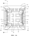
Fig. 1A is a top view of a circuit-board assembly in accordance with one embodiment; -
Fig. 1B is a cross section view along section A-A of the circuit-board assembly ofFig. 1A in accordance with one embodiment; -
Fig. 1C is a cross section view along section B-B of the circuit-board assembly ofFig. 1A in accordance with one embodiment; -
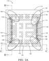
Fig. 2A is a top view of a circuit-board assembly in accordance with another embodiment; and -
Fig. 2B is a cross section view along section C-C of the circuit-board assembly ofFig. 2A in accordance with one embodiment; and -
Fig. 2C is a cross section view along section D-D of the circuit-board assembly ofFig. 2A in accordance with one embodiment; - The reference numbers of similar elements in the embodiments shown in the various figures share the last two digits.
-
Figs. 1A - 1C illustrate a non-limiting example of one embodiment of circuit-board assembly 10 that includes a printed circuit-board 12 (hereafter referred to as the PCB 12), an integrated-circuit die 14 (hereafter referred to as the IC-die 14), a ball grid-array 16 (hereafter referred to as the BGA 16), abarrier material 18, and anadhesive material 20. - The
PCB 12 may be formed of circuit board substrates that are made of epoxy-resins or polyimide-resins. The resin may be reinforced with a woven glass cloth or other matrix such as chopped fibers. Substrates formed of such materials are typically referred to as FR-4 or G-10 type circuit boards. The circuit board substrate may alternatively be constructed of ceramic or rigid polymer materials. This listing of acceptable substrate materials is not exhaustive and other materials may also be used successfully. ThePCB 12 may also include various electronic components (not shown) including, but not limited to, capacitors, resistors, inductors, amplifiers, micro-processors, etc. as will be recognized by one skilled in the art. ThePCB 12 includes amounting surface 22 that defines a plurality ofcontact pads 24 and defines acontinuous trace 26 that interconnects a selectedgroup 28 of thecontact pads 24. Thecontact pads 24 and thecontinuous trace 26 may be formed by chemically etching a continuous layer of conductive material, such as a copper-based material, that may be deposited on the circuit board sub strate. - The IC-
die 14 includes anelectrical circuit 30 that has a plurality ofsolder pads 32. Thesolder pads 32 may provide an electrical path through the IC-die 14, as will be recognized by those in the art. Theelectrical circuit 30 may be anyelectrical circuit 30, including, but not limited to, a monolithic microwave integrated-circuit 34 (MMIC 34) as illustrated inFigs. 1A - 1C . - The BGA 16 includes a plurality of
solder balls 36 interposed between thecontact pads 24 and thesolder pads 32. The plurality ofsolder balls 36 establish electrical communication between theelectrical circuit 30 and thecontact pads 24 when the circuit-board assembly 10 is assembled. The typical assembly process may include placing thePCB 12 and the IC-die 14 in an oven heated to a melting temperature of the solder balls 36 (typically 250°C) where the solder melts and reflows creating a metallurgical bond between the IC-die 14 and thecontact pads 24 upon cooling to a temperature below the melting temperature of the solder. - The
barrier material 18 is located between astring 38 ofsolder balls 36 that are attached to the selectedgroup 28 of thecontact pads 24 to create abarrier 40. Thebarrier 40 segregates anunderfill region 42 from anon-underfill region 44 between thePCB 12 and the IC-die 14, whereby thebarrier 40 is in direct contact with thestring 38 of thesolder balls 36, the IC-die 14, and thecontinuous trace 26. - The
adhesive material 20 is in direct contact with a portion of theunderfill region 42, whereby thebarrier 40 prevents theadhesive material 20 from encroaching upon thenon-underfill region 44. The typicaladhesive material 20 may be applied at room temperature after the circuit-board assembly 10 is assembled (i.e. after the solder reflow process) as described above, and may flow around solder joints between the IC-die 14 and thePCB 12 until cured. Theadhesive material 20 may also be cured at an elevated temperature according to the manufacturer's guidelines. The adhesive material 20 (also referred to as "underfill", "corner bond", "edge bond", etc.) is designed to improve reliability of the circuit-board assembly 10, specifically improving the fatigue strength of the solder joints during thermal cycling. Theadhesive material 20 may also improve reliability during bending and mechanical shock. Many commercialadhesive material 20 products exist, and those skilled in the art may select a particular product that meets the requirements for their particular application. One suchadhesive material 20 is G5602 manufactured by Stick1 Material, Inc. of Pleasanton, California, USA. Theadhesive material 20 may preferably be an epoxy suitable for use with electrical components, such as LOCTITE ® ECCOBOND E 1216M, manufactured by Henkel AG & Company, of Dusseldorf, Germany. - The
barrier material 18 may be aconductive solder 46, such as ALPHA ® OM-340 supplied by Cookson Electronics of South Plainfield, New Jersey, USA. Thestring 38 ofsolder balls 36 may be metallurgically bonded to thesolder pads 32 and thecontinuous trace 26, and theconductive solder 46 may be metallurgically bonded to thesolder balls 36 and thecontinuous trace 26. - In the non-limiting example illustrated by
Figs. 1A - 1C , the IC-die 14 contains theMMIC 34 and thebarrier 40 may provide aground path 48 for theelectrical circuit 30. Thenon-underfill region 44 may containsolder balls 36 that may propagate radio-frequency signals 50 between thePCB 12 and the IC-die 14. Thebarrier 40 may advantageously prevent theadhesive material 20 from contacting thesolder balls 36 that may propagate the radio-frequency signals 50. This is advantageous because it may eliminate any detrimental impact on both an electrical performance of theMMIC 34, and on an impedance of the conductive traces of thePCB 12, that may result from a dielectric property of theadhesive material 20. - The
barrier material 18 may also be an electrically-conductive epoxy that is compatible with the solder reflow process, such as ABLEBOND ® 967-1™ manufactured by Henkel AG & Company, of Dusseldorf, Germany. Thebarrier material 18 may also be applied to the IC-die 14 and/or to thePCB 12 prior to the mounting of the IC-die 14. -
Figs. 1A - 1C illustrate the IC-die 14 that is rectangular 52 and theadhesive material 20 is located beneathcorners 54 of the IC-die 14. This application location is advantageous because the solder joints located near thecorners 54 typically have a greater incidence of mechanical failure, compared to the solder joints at other locations. -
Figs. 2A - 2C illustrate a non-limiting example of another embodiment of a circuit-board assembly 110 that includes a printed circuit-board 112 (hereafter referred to as the PCB 112), an integrated-circuit die 114 (hereafter referred to as the IC-die 114), a ball grid-array 116 (hereafter referred to as the BGA 116), abarrier material 118, and anadhesive material 120. - The
PCB 112 includes a mountingsurface 122 that defines a plurality ofcontact pads 124 and further defines a selectedgroup 128 of thecontact pads 124. Thecontact pads 124 may be formed by chemically etching a continuous layer of conductive material, such as a copper based material, that is deposited on the circuit board substrate. - The IC-die 114 includes an
electrical circuit 130 that has a plurality ofsolder pads 132. Thesolder pads 132 may provide an electrical path through the IC-die 114, as will be recognized by those in the art. Theelectrical circuit 130 may be anyelectrical circuit 130, including, but not limited to, a monolithic microwave integrated-circuit 134 (MMIC 134) as illustrated inFigs. 2A - 2C . - The
BGA 116 includes a plurality ofsolder balls 136 interposed between thecontact pads 124 and thesolder pads 132. The plurality ofsolder balls 136 may establish electrical communication between theelectrical circuit 130 and thecontact pads 124 when the circuit-board assembly 110 is assembled. The typical assembly process may include placing thePCB 112 and the IC-die 114 in an oven heated to a melting temperature of the solder balls 136 (typically 250°C) where the solder melts and reflows creating a metallurgical bond between the IC-die 114 and thecontact pads 124 upon cooling to a temperature below the melting temperature of the solder. - The
barrier material 118 is located between astring 138 ofsolder balls 136 that are attached to the selectedgroup 128 of thecontact pads 124 to create abarrier 140. Thebarrier 140 segregates anunderfill region 142 from anon-underfill region 144 between thePCB 112 and the IC-die 114, whereby thebarrier 140 is in direct contact with thestring 138 of thesolder balls 136, the IC-die 114, and thePCB 112. - The
adhesive material 120 is in direct contact with a portion of theunderfill region 142, whereby thebarrier 140 prevents theadhesive material 120 from encroaching upon thenon-underfill region 144. The typicaladhesive material 120 may be applied at room temperature after the circuit-board assembly 110 is assembled (i.e. after the solder reflow process) as described above, and may flow around solder joints between the IC-die 114 and thePCB 112 until cured. Theadhesive material 120 may also be cured at an elevated temperature according to the manufacturer's guidelines. The adhesive material 120 (also referred to as "underfill", "corner bond", "edge bond", etc.) is designed to improve reliability of the circuit-board assembly 110, specifically improving the fatigue strength of the solder joints during thermal cycling. Theadhesive material 120 may also improve reliability during bending and mechanical shock. Many commercialadhesive material 120 products exist, and those skilled in the art may select a particular product that meets the requirements for their particular application. One suchadhesive material 120 is G5602 manufactured by Stick1 Material, Inc. of Pleasanton, California, USA. Theadhesive material 120 may preferably be an epoxy suitable for use with electrical components, such as LOCTITE ® ECCOBOND E 1216M, manufactured by Henkel AG & Company, of Dusseldorf, Germany. - In the non-limiting example illustrated by
Figs. 2A - 2C , the IC-die 114 contains theMMIC 134 and thebarrier 140 may provide aground path 148 for theelectrical circuit 130. Thenon-underfill region 144 may containsolder balls 136 that may propagate radio-frequency signals 150 between thePCB 112 and the IC-die 114. Thebarrier 140 may advantageously prevent theadhesive material 120 from contacting thesolder balls 136 that may propagate the radio-frequency signals 150. This is advantageous because it may eliminate any detrimental impact on both an electrical performance of theMMIC 134, and on an impedance of the conductive traces of thePCB 112, that may result from a dielectric property of theadhesive material 120. - The
barrier material 118 may also be an electrically-conductive epoxy that is compatible with the solder reflow process, such as ABLEBOND ® 967-1™ manufactured by Henkel AG & Company, of Dusseldorf, Germany. Thebarrier material 118 may also be applied to the IC-die 114 and/or to thePCB 112 prior to the mounting of the IC-die 114. -
Figs. 2A - 2C illustrate the IC-die 114 that is rectangular 152 and theadhesive material 120 is located beneathcorners 154 of the IC-die 114. This application location is advantageous because the solder joints located near thecorners 154 typically have a greater incidence of mechanical failure, compared to the solder joints at other locations. - Accordingly, a circuit-
board assembly 10 is provided. The circuit-board assembly 10 includes thebarrier 40 that advantageously prevents theadhesive material 20 from encroaching upon thenon-underfill region 44. This is advantageous because it eliminates any detrimental impact on both the electrical performance of theelectrical circuit 30, and on the impedance of the conductive traces of thePCB 12, that may result from the dielectric property of theadhesive material 20. - While this invention has been described in terms of the preferred embodiments thereof, it is not intended to be so limited, but rather only to the extent set forth in the claims that follow. Moreover, the use of the terms first, second, etc. does not denote any order of importance, but rather the terms first, second, etc. are used to distinguish one element from another. Furthermore, the use of the terms a, an, etc. do not denote a limitation of quantity, but rather denote the presence of at least one of the referenced items. Additionally, directional terms such as upper, lower, etc. do not denote any particular orientation, but rather the terms upper, lower, etc. are used to distinguish one element from another and locational establish a relationship between the various elements.
Claims (8)
- A circuit-board assembly (10), comprising:a printed circuit-board (12) that includes a mounting surface (22) that defines a plurality of contact pads (24) and a continuous trace (26) that interconnects a selected group (28) of the contact pads (24);an integrated-circuit die (14) that includes an electrical circuit (30), said integrated-circuit die (14) having a plurality of solder pads (32);a ball grid-array (16) that includes a plurality of solder balls (36) interposed between the contact pads (24) and the solder pads (32), said plurality of solder balls (36) establish electrical communication between the electrical circuit (30) and the contact pads (24) when the circuit-board assembly (10) is assembled;a barrier material (18) that is a conductive solder (46) or an electrically-conductive epoxy located between a string (38) of solder balls (36) that are attached to the selected group (28) of the contact pads (24) to create a barrier (40) that segregates an underfill region (42) from a non-underfill region (44) between the printed circuit-board (12) and the integrated-circuit die (14), whereby the barrier (40) is in direct contact with the string (38) of the solder balls (36), the integrated-circuit die (14), and the continuous trace (26); andan adhesive material (20) in direct contact with a portion of the underfill region (42), whereby the barrier (40) prevents the adhesive material (20) from encroaching upon the non-underfill region (44).
- The circuit-board assembly (10) according to claim 1,wherein the barrier material (18) is a conductive solder (46) metallurgically bonded to the solder balls (36) and the continuous trace (26).
- The circuit-board assembly (10) in accordance with claim 2, wherein the string (38) of solder balls (36) are metallurgically bonded to the solder pads (32) and the continuous trace (26).
- The circuit-board assembly (10) in accordance with claim 3, wherein the barrier (40) provides a ground path (48) for the electrical circuit (30).
- The circuit-board assembly (10) according to any one of the claims 3 and 4, wherein the electrical circuit (30) is a monolithic microwave integrated-circuit (34).
- The circuit-board assembly (10) in accordance with claim 5, wherein the non-underfill region (44) contains solder balls (36) that propagate radio-frequency signals (50) between the printed circuit-board (12) and the integrated-circuit die (14).
- The circuit-board assembly (10) according to any one of the preceding claims, wherein the adhesive material (20) is an epoxy.
- The circuit-board assembly (10) according to any one of the preceding claims, wherein the integrated-circuit die (14) is rectangular (52) and the adhesive material (20) is located beneath corners (54) of the integrated-circuit die (14).
Applications Claiming Priority (1)
| Application Number | Priority Date | Filing Date | Title |
|---|---|---|---|
| US15/467,659 US9978707B1 (en) | 2017-03-23 | 2017-03-23 | Electrical-device adhesive barrier |
Publications (3)
| Publication Number | Publication Date |
|---|---|
| EP3383148A2 EP3383148A2 (en) | 2018-10-03 |
| EP3383148A3 EP3383148A3 (en) | 2018-10-10 |
| EP3383148B1 true EP3383148B1 (en) | 2024-05-01 |
Family
ID=61683579
Family Applications (1)
| Application Number | Title | Priority Date | Filing Date |
|---|---|---|---|
| EP18161588.1A Active EP3383148B1 (en) | 2017-03-23 | 2018-03-13 | Electrical-device adhesive barrier |
Country Status (3)
| Country | Link |
|---|---|
| US (1) | US9978707B1 (en) |
| EP (1) | EP3383148B1 (en) |
| CN (1) | CN108633181B (en) |
Families Citing this family (10)
| Publication number | Priority date | Publication date | Assignee | Title |
|---|---|---|---|---|
| JP7298195B2 (en) * | 2019-03-05 | 2023-06-27 | 富士通オプティカルコンポーネンツ株式会社 | Optical module and its manufacturing method |
| US11152226B2 (en) * | 2019-10-15 | 2021-10-19 | International Business Machines Corporation | Structure with controlled capillary coverage |
| US11156346B2 (en) | 2019-11-19 | 2021-10-26 | Lumileds Llc | Fan out structure for light-emitting diode (LED) device and lighting system |
| JP7226274B2 (en) * | 2019-11-29 | 2023-02-21 | 株式会社デンソー | radar equipment |
| US11777066B2 (en) | 2019-12-27 | 2023-10-03 | Lumileds Llc | Flipchip interconnected light-emitting diode package assembly |
| US11664347B2 (en) | 2020-01-07 | 2023-05-30 | Lumileds Llc | Ceramic carrier and build up carrier for light-emitting diode (LED) array |
| CN115485836A (en) * | 2020-03-10 | 2022-12-16 | 亮锐有限责任公司 | Method of manufacturing an enhanced LED array assembly |
| CN114843198B (en) * | 2022-06-21 | 2022-10-14 | 太极半导体(苏州)有限公司 | Warpage prevention BGA chip packaging technology and packaging structure thereof |
| US20240145420A1 (en) * | 2022-10-28 | 2024-05-02 | Intel Corporation | Liquid metal shield for fine pitch interconnects |
| EP4490655B1 (en) * | 2023-03-22 | 2025-12-03 | Smartflex Technology Pte Ltd | Articles of manufacture relating to ic modules and smart cards |
Family Cites Families (14)
| Publication number | Priority date | Publication date | Assignee | Title |
|---|---|---|---|---|
| DE69523010T2 (en) * | 1994-10-04 | 2002-07-04 | Nec Corp., Tokio/Tokyo | Semiconductor package manufactured using automatic tape assembly |
| US5956605A (en) * | 1996-09-20 | 1999-09-21 | Micron Technology, Inc. | Use of nitrides for flip-chip encapsulation |
| JP3612155B2 (en) * | 1996-11-20 | 2005-01-19 | 株式会社日立製作所 | Semiconductor device and lead frame for semiconductor device |
| US6774497B1 (en) * | 2003-03-28 | 2004-08-10 | Freescale Semiconductor, Inc. | Flip-chip assembly with thin underfill and thick solder mask |
| US7166906B2 (en) * | 2004-05-21 | 2007-01-23 | Samsung Electronics Co., Ltd. | Package with barrier wall and method for manufacturing the same |
| JP2006140327A (en) | 2004-11-12 | 2006-06-01 | Matsushita Electric Ind Co Ltd | Wiring board and electronic component mounting method using the same |
| DE102006043215A1 (en) * | 2006-09-11 | 2008-03-27 | Qimonda Ag | Chip i.e. semiconductor chip, coplanar installing method, involves connecting adhesive surfaces with each other by chip and support under adjusting of intermediate area between chip and support |
| JP5211493B2 (en) * | 2007-01-30 | 2013-06-12 | 富士通セミコンダクター株式会社 | Wiring substrate and semiconductor device |
| KR101089956B1 (en) * | 2009-10-28 | 2011-12-05 | 삼성전기주식회사 | Flip chip package and manufacturing method thereof |
| US8399300B2 (en) * | 2010-04-27 | 2013-03-19 | Stats Chippac, Ltd. | Semiconductor device and method of forming adjacent channel and DAM material around die attach area of substrate to control outward flow of underfill material |
| US8916969B2 (en) * | 2011-07-29 | 2014-12-23 | Taiwan Semiconductor Manufacturing Company, Ltd. | Semiconductor devices, packaging methods and structures |
| US8581406B1 (en) * | 2012-04-20 | 2013-11-12 | Raytheon Company | Flip chip mounted monolithic microwave integrated circuit (MMIC) structure |
| US20140291834A1 (en) * | 2013-03-27 | 2014-10-02 | Micron Technology, Inc. | Semiconductor devices and packages including conductive underfill material and related methods |
| JP2015002235A (en) * | 2013-06-14 | 2015-01-05 | パナソニック株式会社 | Electronic component mounting method |
-
2017
- 2017-03-23 US US15/467,659 patent/US9978707B1/en active Active
-
2018
- 2018-03-13 EP EP18161588.1A patent/EP3383148B1/en active Active
- 2018-03-22 CN CN201810239332.3A patent/CN108633181B/en active Active
Also Published As
| Publication number | Publication date |
|---|---|
| EP3383148A2 (en) | 2018-10-03 |
| CN108633181A (en) | 2018-10-09 |
| CN108633181B (en) | 2021-05-07 |
| EP3383148A3 (en) | 2018-10-10 |
| US9978707B1 (en) | 2018-05-22 |
Similar Documents
| Publication | Publication Date | Title |
|---|---|---|
| CN108633181B (en) | Electrical equipment adhesive barrier | |
| US6351393B1 (en) | Electronic package for electronic components and method of making same | |
| US9867296B2 (en) | Printed circuit board and package substrate | |
| JP5517960B2 (en) | Soldering connection pin, semiconductor package substrate using the soldering connection pin, and semiconductor chip mounting method | |
| US20090316373A1 (en) | PCB having chips embedded therein and method of manfacturing the same | |
| US7985926B2 (en) | Printed circuit board and electronic component device | |
| EP1387403A2 (en) | Semiconductor packaging | |
| US20150083476A1 (en) | Device embedded printed circuit board and method of manufacturing the same | |
| US6441486B1 (en) | BGA substrate via structure | |
| JP7291292B2 (en) | Additive manufacturing technology (AMT) inverted pad interface | |
| EP1950806A1 (en) | Interposer with built-in passive part | |
| US20100327452A1 (en) | Mounting structure and method of manufacturing the same | |
| US8829361B2 (en) | Wiring board and mounting structure using the same | |
| JP6083130B2 (en) | Flexible wiring board with reinforcing plate | |
| EP0810654A1 (en) | Ball grid array package with substrate having no through holes or via interconnections | |
| EP1565047A1 (en) | Circuit board surface mount package | |
| US6407927B1 (en) | Method and structure to increase reliability of input/output connections in electrical devices | |
| JP2008283114A (en) | Electronic component mounting wiring board and method for removing electromagnetic noise from electronic component mounting wiring board | |
| KR102268384B1 (en) | Substrate with electronic device embedded therein and manufacturing method thereof | |
| JP2012231085A (en) | Electronic circuit board, portable terminal device having electronic circuit board, and method of manufacturing pad | |
| JP2008004908A (en) | Circuit board | |
| CN115334747B (en) | Circuit board structure and manufacturing method thereof | |
| KR20210006218A (en) | Printed Circuit Board | |
| JP3692810B2 (en) | Semiconductor device and manufacturing method thereof, circuit board, and electronic apparatus | |
| WO2006030352A2 (en) | Electronic device comprising a flexible printed circuit board conductively connected to a metallic stiffener by means of solder |
Legal Events
| Date | Code | Title | Description |
|---|---|---|---|
| PUAI | Public reference made under article 153(3) epc to a published international application that has entered the european phase |
Free format text: ORIGINAL CODE: 0009012 |
|
| STAA | Information on the status of an ep patent application or granted ep patent |
Free format text: STATUS: THE APPLICATION HAS BEEN PUBLISHED |
|
| PUAL | Search report despatched |
Free format text: ORIGINAL CODE: 0009013 |
|
| AK | Designated contracting states |
Kind code of ref document: A2 Designated state(s): AL AT BE BG CH CY CZ DE DK EE ES FI FR GB GR HR HU IE IS IT LI LT LU LV MC MK MT NL NO PL PT RO RS SE SI SK SM TR |
|
| AX | Request for extension of the european patent |
Extension state: BA ME |
|
| AK | Designated contracting states |
Kind code of ref document: A3 Designated state(s): AL AT BE BG CH CY CZ DE DK EE ES FI FR GB GR HR HU IE IS IT LI LT LU LV MC MK MT NL NO PL PT RO RS SE SI SK SM TR |
|
| AX | Request for extension of the european patent |
Extension state: BA ME |
|
| RIC1 | Information provided on ipc code assigned before grant |
Ipc: H05K 1/18 20060101AFI20180903BHEP Ipc: H01L 23/31 20060101ALI20180903BHEP Ipc: H01L 23/498 20060101ALI20180903BHEP Ipc: H01L 23/66 20060101ALI20180903BHEP Ipc: H05K 1/02 20060101ALI20180903BHEP Ipc: H05K 3/34 20060101ALI20180903BHEP |
|
| RAP1 | Party data changed (applicant data changed or rights of an application transferred) |
Owner name: APTIV TECHNOLOGIES LIMITED |
|
| STAA | Information on the status of an ep patent application or granted ep patent |
Free format text: STATUS: REQUEST FOR EXAMINATION WAS MADE |
|
| 17P | Request for examination filed |
Effective date: 20190410 |
|
| RBV | Designated contracting states (corrected) |
Designated state(s): AL AT BE BG CH CY CZ DE DK EE ES FI FR GB GR HR HU IE IS IT LI LT LU LV MC MK MT NL NO PL PT RO RS SE SI SK SM TR |
|
| STAA | Information on the status of an ep patent application or granted ep patent |
Free format text: STATUS: EXAMINATION IS IN PROGRESS |
|
| 17Q | First examination report despatched |
Effective date: 20210416 |
|
| RAP3 | Party data changed (applicant data changed or rights of an application transferred) |
Owner name: APTIV TECHNOLOGIES LIMITED |
|
| RIC1 | Information provided on ipc code assigned before grant |
Ipc: H01L 21/56 20060101ALI20231002BHEP Ipc: H01L 23/00 20060101ALI20231002BHEP Ipc: H01L 23/66 20060101ALI20231002BHEP Ipc: H01L 23/498 20060101ALI20231002BHEP Ipc: H01L 23/31 20060101ALI20231002BHEP Ipc: H05K 3/34 20060101ALI20231002BHEP Ipc: H05K 1/02 20060101ALI20231002BHEP Ipc: H05K 1/18 20060101AFI20231002BHEP |
|
| GRAP | Despatch of communication of intention to grant a patent |
Free format text: ORIGINAL CODE: EPIDOSNIGR1 |
|
| STAA | Information on the status of an ep patent application or granted ep patent |
Free format text: STATUS: GRANT OF PATENT IS INTENDED |
|
| INTG | Intention to grant announced |
Effective date: 20231114 |
|
| RIN1 | Information on inventor provided before grant (corrected) |
Inventor name: IHMS, DAVID W. Inventor name: PEPPLES, MICHAEL J. Inventor name: ZIMMERMANN, DAVID W |
|
| GRAS | Grant fee paid |
Free format text: ORIGINAL CODE: EPIDOSNIGR3 |
|
| GRAA | (expected) grant |
Free format text: ORIGINAL CODE: 0009210 |
|
| STAA | Information on the status of an ep patent application or granted ep patent |
Free format text: STATUS: THE PATENT HAS BEEN GRANTED |
|
| P01 | Opt-out of the competence of the unified patent court (upc) registered |
Effective date: 20240223 |
|
| AK | Designated contracting states |
Kind code of ref document: B1 Designated state(s): AL AT BE BG CH CY CZ DE DK EE ES FI FR GB GR HR HU IE IS IT LI LT LU LV MC MK MT NL NO PL PT RO RS SE SI SK SM TR |
|
| RAP1 | Party data changed (applicant data changed or rights of an application transferred) |
Owner name: APTIV TECHNOLOGIES AG |
|
| REG | Reference to a national code |
Ref country code: GB Ref legal event code: FG4D |
|
| REG | Reference to a national code |
Ref country code: CH Ref legal event code: EP |
|
| REG | Reference to a national code |
Ref country code: IE Ref legal event code: FG4D |
|
| REG | Reference to a national code |
Ref country code: DE Ref legal event code: R096 Ref document number: 602018068786 Country of ref document: DE |
|
| REG | Reference to a national code |
Ref country code: LT Ref legal event code: MG9D |
|
| REG | Reference to a national code |
Ref country code: NL Ref legal event code: MP Effective date: 20240501 |
|
| RAP4 | Party data changed (patent owner data changed or rights of a patent transferred) |
Owner name: APTIV TECHNOLOGIES AG |
|
| PG25 | Lapsed in a contracting state [announced via postgrant information from national office to epo] |
Ref country code: IS Free format text: LAPSE BECAUSE OF FAILURE TO SUBMIT A TRANSLATION OF THE DESCRIPTION OR TO PAY THE FEE WITHIN THE PRESCRIBED TIME-LIMIT Effective date: 20240901 |
|
| PG25 | Lapsed in a contracting state [announced via postgrant information from national office to epo] |
Ref country code: BG Free format text: LAPSE BECAUSE OF FAILURE TO SUBMIT A TRANSLATION OF THE DESCRIPTION OR TO PAY THE FEE WITHIN THE PRESCRIBED TIME-LIMIT Effective date: 20240501 |
|
| PG25 | Lapsed in a contracting state [announced via postgrant information from national office to epo] |
Ref country code: FI Free format text: LAPSE BECAUSE OF FAILURE TO SUBMIT A TRANSLATION OF THE DESCRIPTION OR TO PAY THE FEE WITHIN THE PRESCRIBED TIME-LIMIT Effective date: 20240501 Ref country code: HR Free format text: LAPSE BECAUSE OF FAILURE TO SUBMIT A TRANSLATION OF THE DESCRIPTION OR TO PAY THE FEE WITHIN THE PRESCRIBED TIME-LIMIT Effective date: 20240501 |
|
| PG25 | Lapsed in a contracting state [announced via postgrant information from national office to epo] |
Ref country code: GR Free format text: LAPSE BECAUSE OF FAILURE TO SUBMIT A TRANSLATION OF THE DESCRIPTION OR TO PAY THE FEE WITHIN THE PRESCRIBED TIME-LIMIT Effective date: 20240802 |
|
| PG25 | Lapsed in a contracting state [announced via postgrant information from national office to epo] |
Ref country code: PT Free format text: LAPSE BECAUSE OF FAILURE TO SUBMIT A TRANSLATION OF THE DESCRIPTION OR TO PAY THE FEE WITHIN THE PRESCRIBED TIME-LIMIT Effective date: 20240902 |
|
| REG | Reference to a national code |
Ref country code: AT Ref legal event code: MK05 Ref document number: 1684147 Country of ref document: AT Kind code of ref document: T Effective date: 20240501 |
|
| PG25 | Lapsed in a contracting state [announced via postgrant information from national office to epo] |
Ref country code: NL Free format text: LAPSE BECAUSE OF FAILURE TO SUBMIT A TRANSLATION OF THE DESCRIPTION OR TO PAY THE FEE WITHIN THE PRESCRIBED TIME-LIMIT Effective date: 20240501 |
|
| PG25 | Lapsed in a contracting state [announced via postgrant information from national office to epo] |
Ref country code: ES Free format text: LAPSE BECAUSE OF FAILURE TO SUBMIT A TRANSLATION OF THE DESCRIPTION OR TO PAY THE FEE WITHIN THE PRESCRIBED TIME-LIMIT Effective date: 20240501 |
|
| PG25 | Lapsed in a contracting state [announced via postgrant information from national office to epo] |
Ref country code: AT Free format text: LAPSE BECAUSE OF FAILURE TO SUBMIT A TRANSLATION OF THE DESCRIPTION OR TO PAY THE FEE WITHIN THE PRESCRIBED TIME-LIMIT Effective date: 20240501 |
|
| PG25 | Lapsed in a contracting state [announced via postgrant information from national office to epo] |
Ref country code: PL Free format text: LAPSE BECAUSE OF FAILURE TO SUBMIT A TRANSLATION OF THE DESCRIPTION OR TO PAY THE FEE WITHIN THE PRESCRIBED TIME-LIMIT Effective date: 20240501 |
|
| PG25 | Lapsed in a contracting state [announced via postgrant information from national office to epo] |
Ref country code: LV Free format text: LAPSE BECAUSE OF FAILURE TO SUBMIT A TRANSLATION OF THE DESCRIPTION OR TO PAY THE FEE WITHIN THE PRESCRIBED TIME-LIMIT Effective date: 20240501 |
|
| PG25 | Lapsed in a contracting state [announced via postgrant information from national office to epo] |
Ref country code: PT Free format text: LAPSE BECAUSE OF FAILURE TO SUBMIT A TRANSLATION OF THE DESCRIPTION OR TO PAY THE FEE WITHIN THE PRESCRIBED TIME-LIMIT Effective date: 20240902 Ref country code: PL Free format text: LAPSE BECAUSE OF FAILURE TO SUBMIT A TRANSLATION OF THE DESCRIPTION OR TO PAY THE FEE WITHIN THE PRESCRIBED TIME-LIMIT Effective date: 20240501 Ref country code: NO Free format text: LAPSE BECAUSE OF FAILURE TO SUBMIT A TRANSLATION OF THE DESCRIPTION OR TO PAY THE FEE WITHIN THE PRESCRIBED TIME-LIMIT Effective date: 20240801 Ref country code: NL Free format text: LAPSE BECAUSE OF FAILURE TO SUBMIT A TRANSLATION OF THE DESCRIPTION OR TO PAY THE FEE WITHIN THE PRESCRIBED TIME-LIMIT Effective date: 20240501 Ref country code: LV Free format text: LAPSE BECAUSE OF FAILURE TO SUBMIT A TRANSLATION OF THE DESCRIPTION OR TO PAY THE FEE WITHIN THE PRESCRIBED TIME-LIMIT Effective date: 20240501 Ref country code: IS Free format text: LAPSE BECAUSE OF FAILURE TO SUBMIT A TRANSLATION OF THE DESCRIPTION OR TO PAY THE FEE WITHIN THE PRESCRIBED TIME-LIMIT Effective date: 20240901 Ref country code: HR Free format text: LAPSE BECAUSE OF FAILURE TO SUBMIT A TRANSLATION OF THE DESCRIPTION OR TO PAY THE FEE WITHIN THE PRESCRIBED TIME-LIMIT Effective date: 20240501 Ref country code: GR Free format text: LAPSE BECAUSE OF FAILURE TO SUBMIT A TRANSLATION OF THE DESCRIPTION OR TO PAY THE FEE WITHIN THE PRESCRIBED TIME-LIMIT Effective date: 20240802 Ref country code: FI Free format text: LAPSE BECAUSE OF FAILURE TO SUBMIT A TRANSLATION OF THE DESCRIPTION OR TO PAY THE FEE WITHIN THE PRESCRIBED TIME-LIMIT Effective date: 20240501 Ref country code: ES Free format text: LAPSE BECAUSE OF FAILURE TO SUBMIT A TRANSLATION OF THE DESCRIPTION OR TO PAY THE FEE WITHIN THE PRESCRIBED TIME-LIMIT Effective date: 20240501 Ref country code: BG Free format text: LAPSE BECAUSE OF FAILURE TO SUBMIT A TRANSLATION OF THE DESCRIPTION OR TO PAY THE FEE WITHIN THE PRESCRIBED TIME-LIMIT Effective date: 20240501 Ref country code: AT Free format text: LAPSE BECAUSE OF FAILURE TO SUBMIT A TRANSLATION OF THE DESCRIPTION OR TO PAY THE FEE WITHIN THE PRESCRIBED TIME-LIMIT Effective date: 20240501 Ref country code: RS Free format text: LAPSE BECAUSE OF FAILURE TO SUBMIT A TRANSLATION OF THE DESCRIPTION OR TO PAY THE FEE WITHIN THE PRESCRIBED TIME-LIMIT Effective date: 20240801 |
|
| PG25 | Lapsed in a contracting state [announced via postgrant information from national office to epo] |
Ref country code: DK Free format text: LAPSE BECAUSE OF FAILURE TO SUBMIT A TRANSLATION OF THE DESCRIPTION OR TO PAY THE FEE WITHIN THE PRESCRIBED TIME-LIMIT Effective date: 20240501 |
|
| PG25 | Lapsed in a contracting state [announced via postgrant information from national office to epo] |
Ref country code: EE Free format text: LAPSE BECAUSE OF FAILURE TO SUBMIT A TRANSLATION OF THE DESCRIPTION OR TO PAY THE FEE WITHIN THE PRESCRIBED TIME-LIMIT Effective date: 20240501 |
|
| PG25 | Lapsed in a contracting state [announced via postgrant information from national office to epo] |
Ref country code: CZ Free format text: LAPSE BECAUSE OF FAILURE TO SUBMIT A TRANSLATION OF THE DESCRIPTION OR TO PAY THE FEE WITHIN THE PRESCRIBED TIME-LIMIT Effective date: 20240501 |
|
| PG25 | Lapsed in a contracting state [announced via postgrant information from national office to epo] |
Ref country code: RO Free format text: LAPSE BECAUSE OF FAILURE TO SUBMIT A TRANSLATION OF THE DESCRIPTION OR TO PAY THE FEE WITHIN THE PRESCRIBED TIME-LIMIT Effective date: 20240501 Ref country code: SK Free format text: LAPSE BECAUSE OF FAILURE TO SUBMIT A TRANSLATION OF THE DESCRIPTION OR TO PAY THE FEE WITHIN THE PRESCRIBED TIME-LIMIT Effective date: 20240501 |
|
| PG25 | Lapsed in a contracting state [announced via postgrant information from national office to epo] |
Ref country code: SM Free format text: LAPSE BECAUSE OF FAILURE TO SUBMIT A TRANSLATION OF THE DESCRIPTION OR TO PAY THE FEE WITHIN THE PRESCRIBED TIME-LIMIT Effective date: 20240501 |
|
| PG25 | Lapsed in a contracting state [announced via postgrant information from national office to epo] |
Ref country code: SM Free format text: LAPSE BECAUSE OF FAILURE TO SUBMIT A TRANSLATION OF THE DESCRIPTION OR TO PAY THE FEE WITHIN THE PRESCRIBED TIME-LIMIT Effective date: 20240501 Ref country code: SK Free format text: LAPSE BECAUSE OF FAILURE TO SUBMIT A TRANSLATION OF THE DESCRIPTION OR TO PAY THE FEE WITHIN THE PRESCRIBED TIME-LIMIT Effective date: 20240501 Ref country code: RO Free format text: LAPSE BECAUSE OF FAILURE TO SUBMIT A TRANSLATION OF THE DESCRIPTION OR TO PAY THE FEE WITHIN THE PRESCRIBED TIME-LIMIT Effective date: 20240501 Ref country code: EE Free format text: LAPSE BECAUSE OF FAILURE TO SUBMIT A TRANSLATION OF THE DESCRIPTION OR TO PAY THE FEE WITHIN THE PRESCRIBED TIME-LIMIT Effective date: 20240501 Ref country code: DK Free format text: LAPSE BECAUSE OF FAILURE TO SUBMIT A TRANSLATION OF THE DESCRIPTION OR TO PAY THE FEE WITHIN THE PRESCRIBED TIME-LIMIT Effective date: 20240501 Ref country code: CZ Free format text: LAPSE BECAUSE OF FAILURE TO SUBMIT A TRANSLATION OF THE DESCRIPTION OR TO PAY THE FEE WITHIN THE PRESCRIBED TIME-LIMIT Effective date: 20240501 |
|
| REG | Reference to a national code |
Ref country code: DE Ref legal event code: R097 Ref document number: 602018068786 Country of ref document: DE |
|
| PG25 | Lapsed in a contracting state [announced via postgrant information from national office to epo] |
Ref country code: IT Free format text: LAPSE BECAUSE OF FAILURE TO SUBMIT A TRANSLATION OF THE DESCRIPTION OR TO PAY THE FEE WITHIN THE PRESCRIBED TIME-LIMIT Effective date: 20240501 |
|
| PLBE | No opposition filed within time limit |
Free format text: ORIGINAL CODE: 0009261 |
|
| STAA | Information on the status of an ep patent application or granted ep patent |
Free format text: STATUS: NO OPPOSITION FILED WITHIN TIME LIMIT |
|
| 26N | No opposition filed |
Effective date: 20250204 |
|
| PG25 | Lapsed in a contracting state [announced via postgrant information from national office to epo] |
Ref country code: SI Free format text: LAPSE BECAUSE OF FAILURE TO SUBMIT A TRANSLATION OF THE DESCRIPTION OR TO PAY THE FEE WITHIN THE PRESCRIBED TIME-LIMIT Effective date: 20240501 |
|
| PG25 | Lapsed in a contracting state [announced via postgrant information from national office to epo] |
Ref country code: SE Free format text: LAPSE BECAUSE OF FAILURE TO SUBMIT A TRANSLATION OF THE DESCRIPTION OR TO PAY THE FEE WITHIN THE PRESCRIBED TIME-LIMIT Effective date: 20240501 |
|
| PG25 | Lapsed in a contracting state [announced via postgrant information from national office to epo] |
Ref country code: MC Free format text: LAPSE BECAUSE OF FAILURE TO SUBMIT A TRANSLATION OF THE DESCRIPTION OR TO PAY THE FEE WITHIN THE PRESCRIBED TIME-LIMIT Effective date: 20240501 |
|
| REG | Reference to a national code |
Ref country code: CH Ref legal event code: H13 Free format text: ST27 STATUS EVENT CODE: U-0-0-H10-H13 (AS PROVIDED BY THE NATIONAL OFFICE) Effective date: 20251024 |
|
| PG25 | Lapsed in a contracting state [announced via postgrant information from national office to epo] |
Ref country code: LU Free format text: LAPSE BECAUSE OF NON-PAYMENT OF DUE FEES Effective date: 20250313 |
|
| REG | Reference to a national code |
Ref country code: BE Ref legal event code: MM Effective date: 20250331 |
|
| PG25 | Lapsed in a contracting state [announced via postgrant information from national office to epo] |
Ref country code: BE Free format text: LAPSE BECAUSE OF NON-PAYMENT OF DUE FEES Effective date: 20250331 |
|
| PG25 | Lapsed in a contracting state [announced via postgrant information from national office to epo] |
Ref country code: CH Free format text: LAPSE BECAUSE OF NON-PAYMENT OF DUE FEES Effective date: 20250331 |
|
| PG25 | Lapsed in a contracting state [announced via postgrant information from national office to epo] |
Ref country code: IE Free format text: LAPSE BECAUSE OF NON-PAYMENT OF DUE FEES Effective date: 20250313 |
|
| PGFP | Annual fee paid to national office [announced via postgrant information from national office to epo] |
Ref country code: GB Payment date: 20260204 Year of fee payment: 9 |
|
| PGFP | Annual fee paid to national office [announced via postgrant information from national office to epo] |
Ref country code: DE Payment date: 20260223 Year of fee payment: 9 |
|
| PGFP | Annual fee paid to national office [announced via postgrant information from national office to epo] |
Ref country code: FR Payment date: 20260205 Year of fee payment: 9 |